solar energy materials & solar cells - uji · (20 nm)/gold (100 nm) triangle contacts were...
TRANSCRIPT

Diamond-based electrodes for organic photovoltaic devices
Alexander Kovalenko a,b,n, Petr Ashcheulov c,d, Antonio Guerrero b, Patricie Heinrichová a,Ladislav Fekete c, Martin Vala a, Martin Weiter a, Irena Kratochvílová c,Germà Garcia-Belmonte b
a Brno University of Technology, Faculty of Chemistry, Materials Research Centre, Purkyňova 118, 612 00 Brno, Czech Republicb Photovoltaic and Optoelectronic Devices Group, Departament de Física, Universitat Jaume I, ES-12071 Castelló, Spainc Institute of Physics, Academy of Sciences Czech Republic v.v.i., Na Slovance 2, CZ-182 21 Prague 8, Czech Republicd Faculty of Nuclear Physics and Physical Engineering, Czech Technical University in Prague, Zikova 1, 160 00 Prague 6, Czech Republic
a r t i c l e i n f o
Article history:Received 25 September 2014Received in revised form10 November 2014Accepted 15 November 2014Available online 5 December 2014
Keywords:Organic photovoltaicsBoron doped diamondChemical vapor depositionTransparent electrodes
a b s t r a c t
The present paper demonstrates the possibility of replacing indium–tin oxide (ITO) with heavily boron-doped diamond (BDD). Plasma Enhanced Chemically Vapor Deposited BDDs layers of various thicknesseswere prepared containing various boron concentrations in a gas phase. The dependence of the above-mentioned parameters on the optical and electrical properties of each BDD was studied in order toachieve optimal conditions for the effective application of diamond electrodes in organic electronics as areplacement for ITO. Bulk-heterojunction polymer–fullerene organic solar cells were fabricated to testthe potency of BDD application in photovoltaic devices. The obtained results demonstrated thepossibility of the aforementioned application. Even though the efficiency of BDD-based devices is lowercompared to those using regular ITO-based architecture, the relevant issues were explained.
& 2014 Elsevier B.V. All rights reserved.
1. Introduction
Today, the development potential of organic electronics canhardly be overestimated [1]. In an age of silicon devices, it is worthnoting that, although silicon is inexhaustible, its purification,processing and utilization are not as ecologically friendly as couldbe desired. Organic electronic devices, meanwhile, are beginningto enter many fields of science and technology due to their manyclear advantages. Owing to its low production temperatures,organic electronics does not require large energy consumption,which makes such electronics, along with the non-toxicity of itscomponent materials, much more environmentally friendly incomparison with commonly used inorganic semiconductors. Simi-lar to silicon, organic materials are practically unlimited, but mucheasier to utilize. Specifically, due to their particular properties,they are flexible, adaptive to many types of surfaces, and virtuallyunbreakable.
In spite of the fact that organic electronics seems to be thetechnology of the future, some technological steps remain un- orunderdeveloped, which significantly thwarts the infusion of thistechnology. Considering organic solar cells, which seem to haveparticular potential, one of the limiting factors is the development oftransparent electrodes. At first glance, the widely-used compound
indium–tin oxide (ITO) seems to be the perfect candidate as amaterial for transparent electrode, as it exhibits superior transpar-ency and a sheet resistance of below 100Ω/sq. However, thedeclining availability of indium compels us to look for an alternativesolution.
One possibility is to substitute ITO with carbon-based electrodessuch as heavily boron-doped conductive diamond polycrystallinefilms [2]. Polycrystalline diamond films can be produced by a largevariety of chemical deposition techniques, such as hot filamentdeposition [3], bias enhanced deposition [4], and Plasma-EnhancedChemical Vapor Deposition (PECVD) with linear antenna delivery,where precursor gases are ionized to enhance their chemicalreaction rates [5,6]. One of the advantages of the PECVD techniqueis the possibility to operate on a large variety of substrates at lowdeposition temperatures, which can be a crucial condition in themanufacture of semiconductors. With respect to photovoltaicdevices, light-harvesting materials can be directly manufactured bythe PECVD process [7,8]. Diamond is recognized to be a remarkablematerial due to its particularly attractive properties combiningchemical resistance, optical transparency, thermal conductivity [9–13], and electrochemical properties [14–18]. Once successfullydoped, diamond, which is generally recognized as an insulatingmaterial, becomes a wide-band gap semiconductor material withexcellent potential due to the unique combination of its physical andelectronic properties. The boron atom seems to be the only efficientdopant atom in diamond, which can be incorporated with highreproducibility and at a concentration high enough to be useful for
Contents lists available at ScienceDirect
journal homepage: www.elsevier.com/locate/solmat
Solar Energy Materials & Solar Cells
http://dx.doi.org/10.1016/j.solmat.2014.11.0350927-0248/& 2014 Elsevier B.V. All rights reserved.
n Corresponding author: Tel: þ420 775377415.E-mail address: [email protected] (A. Kovalenko).
Solar Energy Materials & Solar Cells 134 (2015) 73–79

electronic devices [15–19]. The physical properties of lightly-dopedsemiconductors are described in terms of band structures andimpurity levels – the phenomenon of the formation of an impurityband was observed even at room temperature [17,18]. In the presentpaper, the possibility of replacing ITO with boron-doped diamond isdescribed.
The addition of boron has a strong influence on the electricalconductivity of diamond layers [19–27]. For moderate boronconcentrations – below 3�1020 cm�3 – standard conductivityvalues for diamond layers were found [19,28]. Higher boronconcentrations typically result in conductive systems with elec-trical properties comparable to those of metallic materials; also,superconductivity was reported by Ekimov et al. [15] in heavily B-doped diamond. There are also other parameters which influenceboron-doped diamond layer charge transport properties – namely,the electronic structures of boron defects, the morphology of thenanodiamond layer (the addition of boron has a strong influenceon the morphology of the layers grown [20]), and the relativeamount of sp2 and sp3 hybridized carbon in the nanodiamondlayer [29–31]. The optimization of growth conditions at highboron/carbon ratios (up to 8000 ppm in the gas phase duringgrowth) can lead to low sheet resistance comparable to, or evenlower than those of the best ITO samples.
2. Experimental
2.1. Diamond electrodes fabrication
One of the main tasks was the proper patterning of the glasssubstrates for the subsequent measurements of the solar cells'power conversion efficiency (PCE). Prior to the growth of thediamond layer, glass substrates were screened with a patternmask, which enabled the area on top of the substrates to becovered with electrode channels 8 mm in width. The substrateswere then seeded with a nanodiamond particle solution whichwas sonicated before seeding in order to break up large clusters indispersion. The mean size of the nanodiamond seeds in thesolution was 5–10 nm as measured by dynamic light scattering(DLS) after sonication. Then, the glass substrates were cleaned inisopropyl alcohol (IPA) and subsequently dipped into the diamonddispersion. In order to produce a monolayer of nanodiamondseeds on the glass substrate surface, the seeding solution wasdeposited by spin coating for 30 s at 3000 rpm. This procedureresulted in homogenous coverage of the patterned substrates witha nucleation seed density of approximately 1010 cm�2 as measuredby Atomic Force Microscopy (AFM).
After the patterned seeding on glass substrates was prepared,boron-doped diamond (BDD) nanocrystalline films were grown by achemical vapor deposition technique. A SEKI ASTeX 5010 Micro-wave Plasma Enhanced CVD reactor was used to grow the BDDlayers. Growth was performed in CH4/H2 plasma with a respectivegas concentration ratio of 5%/95%. Boron doping was achieved byadding trimethylboron (TMB) to the gas mixture. The substratetemperature (700 1C) during the BDD growth process was mon-itored by a Williamson Pro 92-38 dual-wavelength infrared pyrom-eter. By varying the B/C concentrations (from 2000 to 8000 ppm)during the growth process, layers with different doping levels wereobtained. In order to obtain optically transparent electrodes, BDDlayers with various thicknesses were produced.
2.2. Diamond film characterization techniques
Several characterization techniques were applied to investigatethe properties of the boron-doped diamond films. In order toreveal the sp3/sp2 ratio (the presence of amorphous and graphitic
phases) throughout the layer, Raman spectroscopy measurementswere carried out. Spectra were taken at room temperature using aRenishaw InVia Raman microscope under the following condi-tions: wavelength – 488 nm (25 mW); objective – �50 Olympus;slit size – 65 μm; type of focus – spot focus; grating – 2400 l/mm.
The conductivity and Hall constant were measured by thedifferential van der Pauw method using a Keithley 6221 currentsource and two electrometers, a Keithley 6514 with nano-volt-meter, and a Keithley 2182A, which recorded the voltage differ-ence between the electrometers. A pulsed (quasi-DC) measuringmode was used to compensate for parasitic thermoelectric signals.All electrical measurements were performed in dark at roomtemperature (29671 K). In all films investigated, the resistivitywas measured with an error not exceeding 1–2%, while the Hallconstant and mobility were determined with an accuracy of about5%. For the electrical characterization of BDD films, titanium(20 nm)/gold (100 nm) triangle contacts were evaporated.
Surface roughness, morphology, and film thickness were inves-tigated by AFM using an NTEGRA Prima NT-MDT system underambient conditions. Samples were scanned using a HA_NC Etalontip in semi-contact mode. A local contrast (LC) filter was applied toall images to better visualize each film's morphology.
The transmittance spectra of samples were characterized by aVarian Cary Probe 50 UV–vis spectrometer (Agilent TechnologiesInc., Santa Clara, CA, U.S.A.). The integral value of transmittancewas determined by integrating spectral data in the range 300–850 nm. Commercially available ITO/glass reference substrateswere purchased from Sigma-Aldrich. The thickness of the refer-ence ITO samples was 60-100 nm, with an electrical conductivityof �50Ω/sq, as measured by a 4 probes method.
2.3. Materials
P3HT (Luminescence Technology Corp.), PC60BM (Solenne,99%), o-dichlorobenzene (Aldrich, 99.9%), ZnO nanoparticles dis-persed in IPA (Gene's Ink), Ca (Aldrich, 99.995%), MoO3 (Aldrich,99.98%) and Ag (Aldrich, 99.99%) were used as received withoutfurther purification. The active layer films were prepared from aP3HT:PC60BM solution (1:0.8 by weight) in o-dichlorobenzene andwere stirred for 12 h at 80 1C until complete dissolution. Theconcentrations of the pure P3HT and PC60BM solutions in o-dichlorobenzene solvent were 17 mg mL�1 and 13.6 mg mL�1,respectively. All manipulations were carried out in a glove boxunder a nitrogen atmosphere unless otherwise stated.
2.4. Device fabrication
Inverted architecture P3HT:PC60BM devices were fabricatedusing the regular procedure [32–34]. After boron-doped diamondelectrodes were grown, substrates were cleaned ultrasonically in10% NaOH solution for 5 min, in deionized water for 15 min, andfinally in IPA for 10 min to remove residual impurities. The cleanedsubstrates were covered by a ZnO suspension by spin-coating at2000 rpm for 40 s at ambient atmosphere, and further annealed at75 1C for 45 s. Prior to deposition, the ZnO was filtered through a0.45 mm nylon filter.
100 nm polymer–fullerene heterojunction layers were preparedby spin coating 55 μl of P3HT:PC60BM solution at 1200 rpm for 15 sin a nitrogen atmosphere and then immediately placed into a closedpetri dish for 60 min for solvent annealing. The devices were furtherthermally annealed at 130 1C for 10 min. Top electrodes (7 nm ofMoO3 and the subsequent evaporation of 100 nm of Ag) weredeposited by vacuum evaporation.
A. Kovalenko et al. / Solar Energy Materials & Solar Cells 134 (2015) 73–7974

2.5. Solar cell characterization techniques
Current density–voltage measurements were carried out underillumination using an Abet Sun 2000 solar simulator with an airmass (AM) 1.5G filter. The simulated light intensity was adjusted to1000 Wm�2 by using an NREL-calibrated Si solar cell.
Capacitance–voltage and impedance spectroscopy data wereacquired using an Autolab PGSTAT-30 equipped with a frequencyanalyzer module.
3. Results and discussion
3.1. Diamond layers characterization
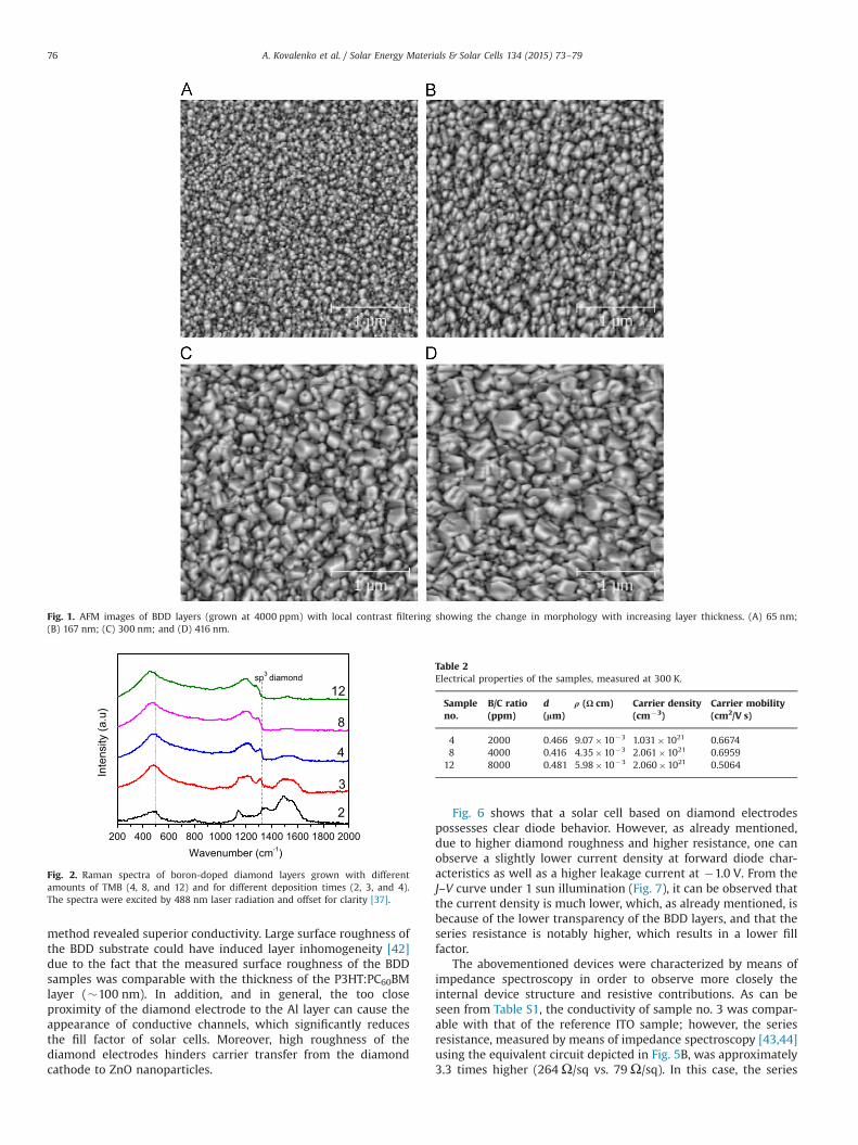
Electrical measurements revealed that the conductivity of theBDD layers is correlated to the size of the grains in the layer.Indeed, for the same B/C ratio, thicker layers are less resistive, ascan be seen from Tables 1 and S1. This effect is attributed to thesize of the grains [30], as confirmed by AFM scans (Fig. 1). Themagnitude of the sheet resistance, measured by the 4 point probestechnique, was in the range from 21Ω/sq for the 481 nm thicksample prepared at an 8000 ppm B/C ratio to 5�104Ω/sq for thethin 70 nm diamond grown at the 2000 ppm B/C ratio (Table 1).Notably, the sheet resistance of the reference ITO sample was50Ω/sq. Conductivity was found to be higher for thicker filmswith the same B content. One of the factors affecting conductivityis grain size. It has been reported [30] that films with a larger grainsize possess higher conductivity due to the higher amount ofboron atoms incorporated into the diamond lattice, while in thecase of smaller grain size films, a large amount of boron is locatedat the grain boundaries, which is consistent with previouslyreported theoretical predictions [35]. Although in the present case,metallic conductivity is highly desired, in the case of largerdiamond grains a high degree of roughness can adversely affectthe further processes of organic layer preparation.
Of all of the grown samples (Table 1), sample no. 3 (the�290 nm thick diamond) exhibited good conductivity with asheet resistance of 50Ω/sq and a decent integral transparencyvalue in the measured wavelength range of around 40%, which ispromising for ITO replacement applications. Thicker heavilyboron-doped samples, i.e. those possessing better conductivity (asheet resistance of up to 21Ω/sq for sample no. 12), were muchless transparent, and were not considered suitable for the desiredapplication. Detailed data are shown in Table S1.
All layers were investigated by AFM (see Fig. 1) and were foundto be free of pinholes. The layers exhibited a distinct crystallinestructure with grains showing a mixture of orientations.
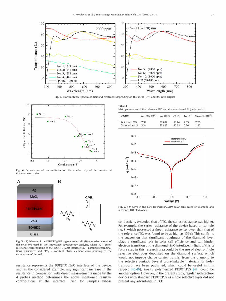
Using Raman spectroscopy, peaks related to diamond (sp3) andgraphitic or amorphous carbon (sp2) were detected for all layersinvestigated (Fig. 2). A diamond peak was observed at 1322 cm�1
as well as broad features at 1150 cm�1 and 1490 cm�1, generallyaccepted as originating from transpolyacetylene at grain bound-aries. Additional features were seen upon an increase in depositiontime and TMB content, i.e. the appearance of broad peaks centeredat 500 and 1225 cm�1, which were related to a locally distortedlattice structure induced by the addition of boron atoms. Thecrystalline diamond peak frequency exhibited a shift towards alower wavenumber (�1295 cm�1) upon increasing B content. Theshift in frequency towards lower wavenumbers was seen also forthe broad 500 cm�1 band. Samples grown for longer depositiontimes exhibited an asymmetry (1250-1328 cm�1) in the spectradue to Fano-type interference between the discrete zone-centerphonon and the continuum electronic states [36]. Notably, theFano resonance just quenches the diamond line and does notmean a worsening of diamond quality.
From Table 2, which shows the electrical properties of thediamond samples grown at various B/C concentrations, it can beseen that, at the 4000 ppm B/C ratio, the concentration of carrierssaturates to its maximum value, which can be explained by thedominant formation of boron–boron centers, as discussed in [37];also as observed on the Raman spectra (Fig. 2) – the B–B peakincreases both with B/C concentration and layer thickness. Thedrop in carrier mobility for sample no. 12 can be explained by theincreasing concentration of scattering centers (defects) differentfrom the regular B acceptors. All the samples under study had acarrier density exceeding 1021 cm�3, which is a characteristic ofmetallic conductivity. Compared to the carrier mobility of ITO (10–50 cm2/V s [38,39]), that for diamond was determined to be twoorders of magnitude lower.
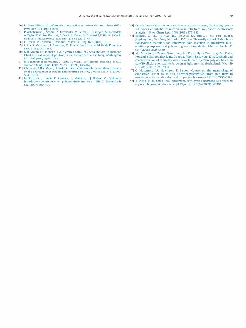
Fig. 3 depicts the dependences of diamond layer transmittanceon layer thickness and B/C ratio. One can notice that the transmit-tance in the UV and visible spectra decreases with both theaugmentation of boron during diamond growth and increasinglayer thickness. The interpolated dependence of transmittance onconductivity is shown in Fig. 4. As can be observed, highlytransparent diamond samples do not exhibit good conductivity;the most conductive sample with a transmittance of over 70% hada resistance 4103 Ω/sq. For highly conductive BDD samples, thebest transparency values achieved were about 40%.
Considering further aspects of the transparency vs. conduc-tance issue, it can be noted that an increase in crystallite size,which can be controlled during the CVD process [40], willsignificantly decrease the proportion of grain boundaries in BDDfilms; thus, conductivity will significantly increase, although grainboundaries affect the transparency of the films due to the high sp2
ratio. In this case, the problem of greater diamond roughnesscaused by larger crystallite sizes can be solved by the previouslyreported process of plasma diamond polishing [41].
3.2. Solar cells characterization
Bulk-heterojunction solar cells were fabricated according to theaforesaid procedure with the inverted architecture (see Fig. 5A). Asshown in Table S1, out of all the prepared diamond samples thebest efficiency was achieved by the solar cell based on sample no.3 possessing 0.91% of PCE, which was about 40% of that of thereference ITO-based BHJ solar cell. From Table 3 and Fig. 4, it canbe seen that the main losses in efficiency were due to lowertransparency resulting in lower current density in comparisonwith the reference cell; this also resulted in slightly lower Voc.
One of the probable reasons for the reduction in PCE could alsobe the roughness of the BDD electrodes, which was an order ofmagnitude higher than the roughness of commercially availableITO. As suggested by AFM measurements, this effect could haveresulted in high-series resistance, even though the 4 points
Table 1Diamond layer growth parameters:.
Sample no. B/C (ppm) Time (min) d (nm) ρ (Ω/sq)
1 2000 30 71 500002 2000 60 148 9103 2000 120 281 504 2000 240 466 485 4000 30 65 11006 4000 60 167 1407 4000 120 300 398 4000 240 416 269 8000 30 90 185
10 8000 60 114 24011 8000 120 219 8012 8000 240 481 21
A. Kovalenko et al. / Solar Energy Materials & Solar Cells 134 (2015) 73–79 75
method revealed superior conductivity. Large surface roughness ofthe BDD substrate could have induced layer inhomogeneity [42]due to the fact that the measured surface roughness of the BDDsamples was comparable with the thickness of the P3HT:PC60BMlayer (�100 nm). In addition, and in general, the too closeproximity of the diamond electrode to the Al layer can cause theappearance of conductive channels, which significantly reducesthe fill factor of solar cells. Moreover, high roughness of thediamond electrodes hinders carrier transfer from the diamondcathode to ZnO nanoparticles.
Fig. 6 shows that a solar cell based on diamond electrodespossesses clear diode behavior. However, as already mentioned,due to higher diamond roughness and higher resistance, one canobserve a slightly lower current density at forward diode char-acteristics as well as a higher leakage current at �1.0 V. From theJ–V curve under 1 sun illumination (Fig. 7), it can be observed thatthe current density is much lower, which, as already mentioned, isbecause of the lower transparency of the BDD layers, and that theseries resistance is notably higher, which results in a lower fillfactor.
The abovementioned devices were characterized by means ofimpedance spectroscopy in order to observe more closely theinternal device structure and resistive contributions. As can beseen from Table S1, the conductivity of sample no. 3 was compar-able with that of the reference ITO sample; however, the seriesresistance, measured by means of impedance spectroscopy [43,44]using the equivalent circuit depicted in Fig. 5B, was approximately3.3 times higher (264Ω/sq vs. 79Ω/sq). In this case, the series
Fig. 1. AFM images of BDD layers (grown at 4000 ppm) with local contrast filtering showing the change in morphology with increasing layer thickness. (A) 65 nm;(B) 167 nm; (C) 300 nm; and (D) 416 nm.
200 400 600 800 1000 1200 1400 1600 1800 2000
sp3 diamond
12
8
4
3
2
Inte
nsity
(a.u
)
Wavenumber (cm-1)
Fig. 2. Raman spectra of boron-doped diamond layers grown with differentamounts of TMB (4, 8, and 12) and for different deposition times (2, 3, and 4).The spectra were excited by 488 nm laser radiation and offset for clarity [37].
Table 2Electrical properties of the samples, measured at 300 K.
Sampleno.
B/C ratio(ppm)
d(lm)
ρ (Ω cm) Carrier density(cm�3)
Carrier mobility(cm2/V s)
4 2000 0.466 9.07�10�3 1.031�1021 0.66748 4000 0.416 4.35�10�3 2.061�1021 0.6959
12 8000 0.481 5.98�10�3 2.060�1021 0.5064
A. Kovalenko et al. / Solar Energy Materials & Solar Cells 134 (2015) 73–7976
resistance represents the BDD(ITO)/ZnO interface of the device,and, in the considered example, any significant increase in theresistance in comparison with direct measurements made by the4 probes method determines the above mentioned resistivecontributions at the interface. Even for samples whose
conductivity exceeded that of ITO, the series resistance was higher.For example, the series resistance of the device based on sampleno. 8, which possessed a sheet resistance twice lower than that ofthe reference ITO, was found to be as high as 156 Ω. This confirmsthe suggestion that significant roughness of the diamond layerplays a significant role in solar cell efficiency and can hinderelectron transition at the diamond–ZnO interface. In light of this, afuture step in this research area could be the use of electron/holeselective electrodes deposited on the diamond surface, whichwould not impede charge carrier transfer from the diamond tothe selective contact. Several cross-linkable materials for hole-transport have been published, which could be useful in thisrespect [45,46]; in-situ polymerized PEDOT:PSS [47] could beanother option. However, in the present study, regular architecturedevices with standard PEDOT:PSS as a hole selective layer did notpresent any advantages in PCE.
Fig. 3. Transmittance spectra of diamond electrodes depending on thickness (left) and B/C ratio (right).
Fig. 4. Dependence of transmittance on the conductivity of the considereddiamond electrodes.
Fig. 5. (A) Scheme of the P3HT:PC60BM organic solar cell; (B) equivalent circuit ofthe solar cell used in the impedance spectroscopy analysis, where Rs – seriesresistance corresponding to the BDD(ITO)/ZnO interface; R1 – parallel (recombina-tion) resistance; and CPE1 – constant phase element corresponding to thecapacitance of the cell.
Table 3Main parameters of the reference ITO and diamond-based BHJ solar cells:.
Device Jsc (mA/cm2) Voc (mV) FF (%) Eta (%) Rshunt (Ω cm2)
Reference ITO 7.32 565.62 56.74 2.35 9705Diamond no. 3 3.34 533.82 50.68 0.90 1122
Voltage [V]-1.0 -0.5 0.0 0.5 1.0
- j [m
A/c
m2 ]
1e-8
1e-7
1e-6
1e-5
1e-4
1e-3
1e-2
1e-1Reference ITODiamond #3
Fig. 6. J–V curve in the dark for P3HT:PC60BM solar cells based on diamond andreference ITO electrodes.
A. Kovalenko et al. / Solar Energy Materials & Solar Cells 134 (2015) 73–79 77

4. Conclusion
In this paper, the possibility of replacing ITO with boron-dopeddiamond was described. However, the obtained PCE values weremuch lower than the ones using ITO as a transparent electrode.Therefore, diamond could be considered to be a prospectivematerial for electrodes as soon as the issue of transparency vs.conduction is resolved. The values of efficiency achieved can becompared with those obtained using graphene electrodes inorganic BHJ solar cells [48]; however, the applied material is muchcheaper and easier to produce. Nevertheless, “the golden mean”between such parameters as B/C ratio and layer thickness still hasto be found, as well as effective means of modifying such devicesin order to increase PCE, e.g. by reducing diamond roughness,improving the purity of the diamond surface, etc. In addition, theissues of low transparency and low carrier mobility still need to beresolved. Impedance spectroscopy, being a powerful tool for thecharacterization of solar cells, helped to reveal uncertainties in thedevice properties, which are caused mainly by the greater rough-ness of the diamond surface resulting in higher series resistance.
Acknowledgment
This work was supported by the Ministry of Education, Youthand Sport of the Czech Republic, Project no. LO1211; by the GrantAgency of the Czech Republic, Project no. 13-29358S; 14-10279S,Technology Agency of the Czech Republic Grant nos. TA04020156and TA04020156, Generalitat Valenciana (Project ISIC/2012/008,Institute of Nanotechnologies for Clean Energies) and EuropeanR&D Project FP7 ITN Grant no. PITN-GA-2009-238201-MATCON.AK gratefully acknowledges financial support from Brno Universityof Technology via Project CZ.1.07/2.3.00/30.0039. We are gratefulto Pavel Hubik for assistance with Hall measurements.
Appendix A. Supporting information
Supplementary data associated with this article can be found inthe online version at http://dx.doi.org/10.1016/j.solmat.2014.11.035.
References
[1] H. Klauk, Organic Electronics: Materials, Manufacturing, and Applications,Wiley, Hoboken, New Jersey, USA, 2006.
[2] Candy Haley Yi Xuan Lim, Yu Lin Zhong, Stoffel Janssens, Milos Nesladek,Kian Ping Loh, Oxygen-terminated nanocrystalline diamond film as anefficient anode in photovoltaics, Adv. Funct. Mater. 20 (2010) 1313–1318.
[3] R. Haubner, B. Lux, Diamond growth by hot-filament chemical vapor deposi-tion: state of the art, Diam. Relat. Mater. 2 (1993) 1277–1294.
[4] Hiromasa Yagi, Kimihiko Hoshina, Akimitsu Hatta, Toshimichi Ito,Takatomo Sasaki, Akio Hiraki, Initial stage of bias-enhanced diamond nuclea-tion induced by microwave plasma, Jpn. J. Appl. Phys. 36 (1997) 507.
[5] S. Veprek, Plasma-induced and plasma-assisted chemical vapor deposition,Thin Solid Films 130 (1985) 135.
[6] Katsuyuki Okada, Plasma-enhanced chemical vapor deposition of nanocrystal-line diamond, Sci. Technol. Adv. Mater. 8 (2007) 624.
[7] Zhigang Zang, Atsushi Nakamura, Jiro Temmyo, Single cuprous oxide filmssynthesized by radical oxidation at low temperature for PV application, Opt.Express 21 (2013) 11448–11456.
[8] Zhigang Zang, Atsushi Nakamura, Jiro Temmyo, Nitrogen doping in cuprousoxide films synthesized by radical oxidation at low temperature, Mater. Lett.92 (2013) 188–191.
[9] J.E. Field, The Properties of Diamond, Academic Press, New-York, NY, 1979.[10] K. Kobashi, Diamond Films, Elsevier, Oxford, UK, 2005.[11] I. Kratochvílová, A. Kovalenko, F. Fendrych, V. Petráková, S. Záliš, M. Nesládek,
Tuning of nanodiamond particles' optical properties by structural defects andsurface modifications: DFT modeling, J. Mater. Chem. 21 (2011) 18248–18255.
[12] I. Kratochvílová, J. Šebera, P. Ashcheulov, M. Golan, M. Ledvina, J. Míčová,F. Mravec, A. Kovalenko, D. Zverev, B. Yavkin, S. Orlinskii, S. Záliš, A. Fišerová,J. Richter, L. Šefc, J. Turánek, Magnetical and optical properties of nanodia-monds can be tuned by particles surface chemistry: theoretical and experi-mental study, J. Phys. Chem. C 43 (2014) 25245–25252.
[13] I. Kratochvílová, A. Kovalenko, A. Taylor, F. Fendrych, V. Řezáčová, J. Vlček,S. Záliš, J. Šebera, P. Cígler, M. Ledvina, M. Nesládek, Fluorescence of variouslyterminated nanodiamond particles: quantum chemical calculations, Phys.Status Solidi A 207 (2010) 1–4.
[14] S. Koizumi, C. Nebel, M. Nesladek, Physics and Applications of CVD Diamond,Wiley-VCH Verlag GmbH & Co.KGaA, Weinheim, Germany, 2008.
[15] E.A. Ekimov, V.A. Sidorov, E.D. Bauer, N.N. Melnik, N.J. Curro, J.D. Thompson, S.M. Stishov, Superconductivity in diamond, Nature 428 (2004) 542–545.
[16] J. Mort, D. Kuhman, M. Machonkin, et al., Boron doping of diamond thin films,Appl. Phys. Lett. 55 (11) (1989) 1121–1123.
[17] J.C. Bourgoin, J. Krynicki, B. Blanchard, Boron concentration and impurity-to-band activation energy in diamond, Phys. Status Solidi A 52 (1979) 293.
[18] Rinat F. Mamin, Takashi Inushima, Conductivity in boron-doped diamond,Phys. Rev. B 63 (2001) 033201.
[19] Y. Takano, et al., Superconductivity in polycrystalline diamond thin films,Diam. Relat. Mater. 14 (2005) 1936.
[20] H. Okazaki, T. Arakane, K. Sugawara, et al., Photoemission study of electronicstructure evolution across the metalinsulator transition of heavily B-dopeddiamond, J. Phys. Chem. Solids 72 (2011) 582–584.
[21] L.i. Niu, Jia-Qi Zhu, Xiao Han, et al., First principles study of structural,electronic and vibrational properties of heavily boron-doped diamond, Phys.Lett. A 373 (2009) 2494–2500.
[22] J.W. AgerIII, W. Walukiewicz, M. McCluskey, Fano interference of the Ramanphonon in heavily boron-doped diamond films grown by chemical vapordeposition, Appl. Phys. Lett. 66 (5) (1995) 616–618.
[23] R.T. Downs, M. Hall-Wallace, The American mineralogist crystal structuredatabase, Am. Mineral. 88 (2003) 247–250.
[24] T. Hom, W. Kiszenick, Accurate lattice constants from multiple reflectionmesurements II: lattice constants of germanium, silicon and diamond, post B,J. Appl. Crystallogr. 8 (1975) 457–458.
[25] J.P. Perdew, K. Burke, M. Ernzerhof, Generalized gradient approximation madesimple, Phys. Rev. Lett. 77 (1996) 3865.
[26] H.J. Monkhorst, J.D. Pack, On special points for Brillouin zone integrations,Phys. Rev. B 13 (1976) 5188.
[27] S.J. Clark, M.D. Segall, C.J. Pickard, P.J. Hasnip, M.J. Probert, K. Refson, M.C. Payne, First principles methods using CASTEP, Z. Kristallogr. 220 (2005)567–570.
[28] M. Dračínský, L. Benda, P. Bouř, Ab-initio modeling of fused silica, crystalquartz, and water Raman spectra, Chem. Phys. Lett. 512 (2010) 54–59.
[29] Z. Vlčková-Živcová, O. Frank, V. Petrák, H. Tarábková, J. Vacík, M. Nesládek,L. Kavan, Electrochemistry and in-situ Raman spectroelectrochemistry of lowand high quality boron doped diamond layers in aqueous electrolyte solution,Electrochim. Acta 87 (2013) 518–525.
[30] P.W. May, W.J. Ludlow, M. Hannaway, et al., Raman and conductivity studies ofboron-doped microcrystalline diamond, facetted nanocrystalline diamond andcauliflower diamond films, Diam. Relat. Mater. 17 (2008) 105–117.
[31] W. Kaiser, W.L. Bond, Phys. Rev. 115 (1959) 857.[32] A. Ng, et al., Annealing of P3HT:PCBM blend film—the effect on its optical
properties, ACS Appl. Mater. Interfaces 5 (10) (2013) 4247–4259.[33] X. Yang, A. Uddin, Effect of thermal annealing on P3HT:PCBM bulk-
heterojunction organic solar cells: a critical review, Renew. Sustain. EnergyRev. 30 (2014) 324–336.
[34] A. Guerrero, et al., Charge carrier transport and contact selectivity limit theoperation of PTB7-based organic solar cells of varying active layer thickness,J. Mater. Chem. A 1 (39) (2013) 12345–12354.
[35] A.S. Barnard, M. Strernberg, Substitutional boron in nanodiamond, bucky-diamond, and nanocrystalline diamond grain boundaries, J. Phys. Chem. B 110(2006) 19307.
Voltage [V]0.0 0.2 0.4 0.6
- j [m
A/c
m2 ]
0
2
4
6
8Reference ITODiamond #3
Fig. 7. J–V curves of P3HT:PC60BM devices based on diamond and reference ITOelectrodes.
A. Kovalenko et al. / Solar Energy Materials & Solar Cells 134 (2015) 73–7978
[36] U. Fano, Effects of configuration interaction on intensities and phase shifts,Phys. Rev. 124 (1961) 1866.
[37] P. Ashcheulov, J. Šebera, A. Kovalenko, V. Petrák, F. Fendrych, M. Nesládek,A. Taylor, Z. VlckováŽivcová, O. Frank, L. Kavan, M. Dracínský, P. Hubík, J. Vacík,I. Kraus, I. Kratochvílová, Eur. Phys. J. B 86 (2013) 443.
[38] E. Terzini, P. Thilakan, C. Minarini, Mater. Sci. Eng. B77 (2000) 110.[39] C. Liu, T. Matsutani, T. Asanuma, M. Kiuchi, Nucl. Instrum.Methods Phys. Res.
Sect. B 18 (2003) 253.[40] M.B. Moran, L.F. Johnson, K.A. Klemm, Control of Crystallite Size in Diamond
Film Chemical Vapor Deposition, Patent Department of the Navy, Washington,DC, 1992 (navy.reptR….M).
[41] H. Buchkremer-Hermanns, C. Long, H. Weiss, ECR plasma polishing of CVDdiamond films, Diam. Relat. Mater. 5 (1996) 845–849.
[42] C.h. Jonda, A.B.R. Mayer, U. Stolz, Surface roughness effects and their influenceon the degradation of organic light emitting devices, J. Mater. Sci. 3 (5) (2000)5645–5651.
[43] M. Knipper, J. Parisi, K. Coakley, C. Waldauf, C.J. Brabec, V. Dyakonov,Impedance spectroscopy on polymer–fullerene solar cells, Z. Naturforsch.62a (2007) 490–494.
[44] Germà Garcia-Belmonte, Antonio Guerrero, Juan Bisquert, Elucidating operat-ing modes of bulk-heterojunction solar cells from impedance spectroscopyanalysis, J. Phys. Chem. Lett. 4 (6) (2013) 877–886.
[45] Michelle S. Liu, Yu-Hua Niu, Jae-Won Ka, Hin-Lap Yip, F.e.i. Huang,Jingdong Luo, Tae-Dong Kim, Alex K.-Y. Jen, Thermally cross-linkable hole-transporting materials for improving hole injection in multilayer blue-emitting phosphorescent polymer light-emitting diodes, Macromolecules 41(24) (2008) 9570–9580.
[46] M.i. Seon Junga, Woong Shina, Sang Jun Parka, Hyeri Youa, Jung Bae Parka,Hongsuk Suhb, Younhee Limc, Do Yeung Yoonc, J.o.o. Hyun Kim, Synthesis andcharacterization of thermally cross-linkable hole injection polymer based onpoly(10-alkylphenothiazine) for polymer light-emitting diode, Synth. Met. 159(19–20) (2009) 1928–1933.
[47] C. Musumeci, J.A. Hutchison, P. Samorì, Controlling the morphology ofconductive PEDOT by in situ electropolymerization: from thin films tonanowires with variable electrical properties, Nanoscale 5 (2013) 7756–7761.
[48] Y. Wang, et al., Large area, continuous, few-layered graphene as anodes inorganic photovoltaic devices, Appl. Phys. Lett. 95 (6) (2009) 063302.
A. Kovalenko et al. / Solar Energy Materials & Solar Cells 134 (2015) 73–79 79