soc fpga based integration testing platform
TRANSCRIPT

RISTO KUITUNENSOC FPGA BASED INTEGRATION TESTING PLATFORM
Master of Science thesis
Examiner: Prof. Jani BoutellierExaminer and topic approved by theFaculty Council of the Faculty ofComputing and Electrical Engineeringon 30th August 2017

I
ABSTRACT
RISTO KUITUNEN: SoC FPGA based integration testing platformTampere University of TechnologyMaster of Science thesis, 45 pagesJanuary 2018Master’s Degree Programme in Information TechnologyMajor: Pervasive ComputingExaminer: Prof. Jani BoutellierKeywords: SoC FPGA, HW/SW Integration, Integration testing, Test bench
The complexity of designing SoCs is rapidly increasing and the development ofsoftware has a major impact on the overall design cost. Traditionally, the softwaredevelopment could only start after the hardware was complete. Prototyping hasbrought a left-shift to the software development flow. Prototypes are models ofthe hardware and they can be developed in different abstraction levels. With highabstraction level prototypes application development can start in parallel with thehardware design. As the project goes further, more accurate prototypes can be madeand the software development can move down to be more hardware centric.
When both hardware and software design are finished, integration testing betweenthem needs to be done. For this, a hardware accurate prototype is needed to ensurethe correct operation with the final silicon implementation. This HW/SW integra-tion testing can be done with FPGA prototypes. The final Register Transfer Level(RTL) description is synthesized to the FPGA fabric and it is connected to a proces-sor so the software can access the hardware under test. By using an SoC FPGA thathas a processor and the FPGA in the same chip, the physical connection betweenthe processor and the FPGA is already available, reducing the development effortrequired.
In this thesis an SoC FPGA evaluation kit is used to build a test bench for integrationtesting for a project that has its RTL design complete. In the test bench, twohardware Designs Under Test (DUT) are connected to each other and additionaltesting blocks are connected to them: a test pattern generator, an error generatorand data capture logic. The DUTs were controlled with the software drivers undertest and the correctness of test data through the DUTs was observed. The testbench proved to be a viable option for integration testing. Running test cases wasfast with the test bench and the test bench was built in short time , allowing anearly start of integration testing after the RTL is released.

II
TIIVISTELMÄ
RISTO KUITUNEN: SoC-FPGA-pohjainen integraatiotestausalustaTampereen teknillinen yliopistoDiplomityö, 45 sivuaTammikuu 2018Tietotekniikan koulutusohjelmaPääaine: Pervasive ComputingTarkastajat: Prof. Jani BoutellierAvainsanat: SoC FPGA, HW/SW Integrointi, Integraatiotestaus, Testipenkki
SoC-piirien suunnittelun kompleksisuus kasvaa nopeasti, ja yhdeksi suurimmistaSoC projektin kululajeista on noussut ohjelmiston kehitys. Perinteisesti ohjelmis-ton kehitys on voitu aloittaa vasta, kun laitteiston kehitystyö on saatu valmiiksi.Prototyyppauksen avulla ohjelmistokehityksen aloitusajankohtaa on voitu aikaistaa.Prototyypit ovat malleja laitteistosta ja niitä voidaan luoda eri abstraktiotasoisina.Korkean abstraktiotason mallien avulla ohjelmistokehitys voidaan aloittaa laitteis-tokehityksen kanssa rinnakkain. Projektin edetessä voidaan luoda tarkempia proto-tyyppejä, jotka mahdollistavat laitteistoläheisemmän ohjelmiston kehityksen.
Kun sekä laitteisto, että ohjelmisto ovat valmiita, niitä täytyy integraatiotestatayhdessä. Tähän tarvitaan tarkkaa prototyyppiä laitteistosta, jotta toimivuus lop-ullisella piirillä voidaan varmistaa. Tätä laitteiston ja ohjelmiston välistä integraa-tiotestausta voidaan tehdä FPGA-prototyypeillä. Laitteiston rekisteristason ku-vaus syntetisoidaan FPGA-piirille ja se yhdistetään prosessoriin, jotta ohjelmistollasaadaan yhteys testattavaan laitteistoon. Käyttämällä SoC-FPGA piiriä, jossa pros-essori ja FPGA ovat samalla sirulla, fyysinen yhteys prosessorin ja FPGAn välilläon jo valmiina, joten sen suunnitteluun ei kulu resursseja.
Tässä työssä luodaan testipenkki integraatiotestausta varten käyttäen SoC FPGAkehitysalustaa. Testipenkissä on kaksi keskenään yhdistettyä laitteistolohkoa ja ni-ihin yhdistetyt testauslohkot: testidatageneraattori, virhegeneraattori ja datankaap-pauslohko. Testattavia laitteistolohkoja ohjattiin ohjelmistotiimin kehittämällä ohjelmis-tolla ja laitteistolohkojen läpi kulkevan testidatan oikeellisuutta tarkkailtiin. SoCFPGA-alustalle kehitetty testipenkki osoittautui hyödylliseksi integraatiotestaustyökaluksi.Testipenkillä saatiin ajettua nopeasti testiajoja ja se saatiin kehitettyä lyhyessäajassa, mikä mahdollistaa aikaisen integraatiotestauksen aloituksen heti laitteistonrekisteritason kuvauksen valmistuttua.

III
PREFACE
I would like to thank the Nokia SoC SW team in Tampere for giving the topic forthis thesis, it was a fun and a challenging project to make. Thank you Ville forassisting me throughout the project and the rest of the team for making a greatatmosphere to work in.
I would also like to thank my wife Nina for being a great support and taking careof our daughter while I was working on this thesis.
Finally, I would like to thank Jani Boutellier for great feedback and advice, especiallyin the final stretch.

IV
CONTENTS
1. Introduction . . . . . . . . . . . . . . . . . . . . . . . . . . . . . . . . . . . 1
1.1 Motivation . . . . . . . . . . . . . . . . . . . . . . . . . . . . . . . . . 2
1.2 Outline . . . . . . . . . . . . . . . . . . . . . . . . . . . . . . . . . . . 3
2. System on Chip architecture . . . . . . . . . . . . . . . . . . . . . . . . . . 4
2.1 Software subsystem . . . . . . . . . . . . . . . . . . . . . . . . . . . . 5
2.1.1 Software stack . . . . . . . . . . . . . . . . . . . . . . . . . . . . 5
2.2 Hardware subsystem . . . . . . . . . . . . . . . . . . . . . . . . . . . 6
2.2.1 Programmable logic . . . . . . . . . . . . . . . . . . . . . . . . . 6
2.3 Interconnects . . . . . . . . . . . . . . . . . . . . . . . . . . . . . . . 6
2.3.1 AXI4 . . . . . . . . . . . . . . . . . . . . . . . . . . . . . . . . . 7
3. System on Chip prototyping . . . . . . . . . . . . . . . . . . . . . . . . . . 8
3.1 Virtual prototype . . . . . . . . . . . . . . . . . . . . . . . . . . . . . 9
3.2 RTL simulation . . . . . . . . . . . . . . . . . . . . . . . . . . . . . . 10
3.3 FPGA prototype . . . . . . . . . . . . . . . . . . . . . . . . . . . . . 10
3.4 Silicon prototype . . . . . . . . . . . . . . . . . . . . . . . . . . . . . 11
4. System on chip integration testing . . . . . . . . . . . . . . . . . . . . . . . 12
4.1 Logging . . . . . . . . . . . . . . . . . . . . . . . . . . . . . . . . . . 12
4.2 Signal probing . . . . . . . . . . . . . . . . . . . . . . . . . . . . . . . 14
4.3 Data management . . . . . . . . . . . . . . . . . . . . . . . . . . . . . 15
4.3.1 Data generation . . . . . . . . . . . . . . . . . . . . . . . . . . . 16
4.3.2 Data capture . . . . . . . . . . . . . . . . . . . . . . . . . . . . . 17
4.4 Fault injection . . . . . . . . . . . . . . . . . . . . . . . . . . . . . . . 18
5. SoC FPGA prototype test bench . . . . . . . . . . . . . . . . . . . . . . . 19
5.1 Choosing the prototype . . . . . . . . . . . . . . . . . . . . . . . . . . 19
5.2 Used hardware and OS . . . . . . . . . . . . . . . . . . . . . . . . . . 21
5.2.1 Xilinx Zynq ZC706 . . . . . . . . . . . . . . . . . . . . . . . . . . 22
5.3 Design flow . . . . . . . . . . . . . . . . . . . . . . . . . . . . . . . . 22

V
5.3.1 PetaLinux . . . . . . . . . . . . . . . . . . . . . . . . . . . . . . . 23
5.3.2 Vivado . . . . . . . . . . . . . . . . . . . . . . . . . . . . . . . . 24
5.4 Test data management . . . . . . . . . . . . . . . . . . . . . . . . . . 26
5.4.1 Data insertion . . . . . . . . . . . . . . . . . . . . . . . . . . . . 26
5.4.2 Data capture . . . . . . . . . . . . . . . . . . . . . . . . . . . . . 27
5.4.3 Error generation . . . . . . . . . . . . . . . . . . . . . . . . . . . 27
5.4.4 Test bench controls . . . . . . . . . . . . . . . . . . . . . . . . . 30
5.5 Reusability . . . . . . . . . . . . . . . . . . . . . . . . . . . . . . . . 30
5.6 Related work . . . . . . . . . . . . . . . . . . . . . . . . . . . . . . . 31
6. SoC FPGA prototype use case . . . . . . . . . . . . . . . . . . . . . . . . . 34
6.1 Boot . . . . . . . . . . . . . . . . . . . . . . . . . . . . . . . . . . . . 34
6.2 Function calls . . . . . . . . . . . . . . . . . . . . . . . . . . . . . . . 35
6.3 Logs . . . . . . . . . . . . . . . . . . . . . . . . . . . . . . . . . . . . 36
6.4 Resets . . . . . . . . . . . . . . . . . . . . . . . . . . . . . . . . . . . 36
6.5 Single test run . . . . . . . . . . . . . . . . . . . . . . . . . . . . . . . 36
6.5.1 Configure test bench . . . . . . . . . . . . . . . . . . . . . . . . . 38
6.5.2 Start testcase . . . . . . . . . . . . . . . . . . . . . . . . . . . . . 38
6.5.3 Data capture . . . . . . . . . . . . . . . . . . . . . . . . . . . . . 39
6.5.4 Generate error . . . . . . . . . . . . . . . . . . . . . . . . . . . . 40
6.6 Chained tests . . . . . . . . . . . . . . . . . . . . . . . . . . . . . . . 40
7. Results . . . . . . . . . . . . . . . . . . . . . . . . . . . . . . . . . . . . . . 42
7.1 Speed . . . . . . . . . . . . . . . . . . . . . . . . . . . . . . . . . . . 42
7.2 Reliability . . . . . . . . . . . . . . . . . . . . . . . . . . . . . . . . . 43
7.3 Error generation . . . . . . . . . . . . . . . . . . . . . . . . . . . . . . 43
7.4 Viability . . . . . . . . . . . . . . . . . . . . . . . . . . . . . . . . . . 43
7.5 Coverage . . . . . . . . . . . . . . . . . . . . . . . . . . . . . . . . . . 44
8. Conclusion . . . . . . . . . . . . . . . . . . . . . . . . . . . . . . . . . . . . 45
Bibliography . . . . . . . . . . . . . . . . . . . . . . . . . . . . . . . . . . . . 46

VI
ACRONYMS
ADC Analog to Digital Converter. 6, 26
ASIC Application Specific Integrated Circuit. 6, 11
BSP Board Support Package. 23
DAC Digital to Analog Converter. 6, 26
DUT Device Under Test. 2, 3, 16, 17, 19, 21, 26, 33, 37–39, 44, 45
FPGA Field-Programmable Gate Array. 2, 3, 6, 10, 11, 14, 15, 21, 23, 24, 26, 32,35, 42, 44, 45
FSBL First Stage Bootloader. 23, 24, 34, 35
GPU Graphics Processing Unit. 15
GUI Graphical User Interface. 24
HAL Hardware Abstraction Layer. 5
ILA Integrated Logic Analyzer. 24
IP Intellectual Property. 2, 6, 7, 21, 25, 38, 40, 45
OS Operating System. 5, 42, 45
PL Programmable Logic. 4, 6, 15, 27
PS Processor System. 4, 6, 15–17, 27, 30
RAM Random Access Memory. 16
RTL Register Transfer Level. 2, 10
RX Receiver. 19, 26
SoC System on a Chip. 2–6, 8, 10, 12, 18, 21, 22, 25, 26, 32, 44, 45
SRAM Static Random Access Memory. 6
Tcl Tool Command Language. 24

VII
TX Transmitter. 19, 26
UVM Universal Verification Methodology. 1
VHDL VHSIC Hardware Description Language. 31

1
1. INTRODUCTION
Embedded devices usually consist of a processor and separate hardware that needsto be controlled by software executed on the processor. The hardware can be cus-tom logic such as an ASIC or an FPGA, and custom software drivers need to bedeveloped to operate the hardware. Modern development flows allow parallel de-velopment of both hardware and software as shown in Figure 1.1. The hardwareis developed according to specification and can be tested with verification methodssuch as Universal Verification Methodology (UVM). Software is developed based onhardware documentation and is unit tested. After both hardware and software reacha certain maturity level, they need to be tested together. That is called integrationtesting.
Device and I/O description
HW/SW partitioning
HW/SW interface and functional specification
Device driver interface
Device driver design
C/C++ implementation/test
Processor/OS/driver implementation & test
Interface logic
Device and I/O design
HDL implementation
HW logic test
System integration/test
Figure 1.1 Flow diagram of parallel hardware and software design. Adapted from [26]
Integration testing can be challenging if the system is complex. The hardware mustbe physically available or simulated to run the software on it. The physical hardware
1.1. Motivation 2
typically arrives at a late stage in a project. If the integration testing has to waitfor it, it makes the project last longer. To avoid the wait, the hardware can besimulated with software. However, simulating the operating system, hardware andsoftware simultaneously can be computationally very heavy, making the simulationslast long. With Register Transfer Level (RTL) simulation, booting an operatingsystem would take years, making it impractical to test [31].
To overcome the slowness of RTL simulation and avoid the wait for a silicon proto-type, virtual- and Field-Programmable Gate Array (FPGA) prototyping platformscan be used. Virtual prototyping platforms are high-level abstractions of the hard-ware based on the specification instead of the actual RTL design, whereas FPGAprototypes are made by programming the developed RTL design to the configurablelogic of an FPGA.
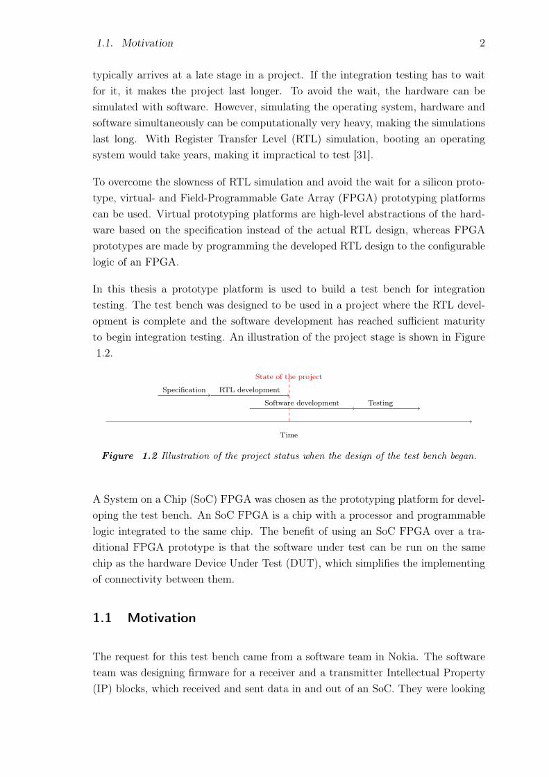
In this thesis a prototype platform is used to build a test bench for integrationtesting. The test bench was designed to be used in a project where the RTL devel-opment is complete and the software development has reached sufficient maturityto begin integration testing. An illustration of the project stage is shown in Figure1.2.
Time
Specification RTL development
Software development Testing
State of the project
Figure 1.2 Illustration of the project status when the design of the test bench began.
A System on a Chip (SoC) FPGA was chosen as the prototyping platform for devel-oping the test bench. An SoC FPGA is a chip with a processor and programmablelogic integrated to the same chip. The benefit of using an SoC FPGA over a tra-ditional FPGA prototype is that the software under test can be run on the samechip as the hardware Device Under Test (DUT), which simplifies the implementingof connectivity between them.
1.1 Motivation
The request for this test bench came from a software team in Nokia. The softwareteam was designing firmware for a receiver and a transmitter Intellectual Property(IP) blocks, which received and sent data in and out of an SoC. They were looking

1.2. Outline 3
for an additional stage to their current integration testing environment. Currentlyintegration testing for the software was done using an environment developed forhardware prototyping, and did not fit well in to software testing. It was a platformwhere an ARM processor and an FPGA were running on separate boards and agolden reference emulator was connected to the FPGA to generate data going in tothe transmitter DUT and verify data coming from the receiver DUT. The platformwas located on another site and controlled remotely. It was slow, shared with mul-tiple users and the remote connection was not stable. The software team wanted tosee if a local test bench could be set up in their site, so they could do testing withthe transmitter and receiver connected to each other (loop testing). With this kindof loop testing, they could test the basic functionality of the software and when thesoftware worked in the loop, they could test it against the golden reference emulatorin the hardware prototyping system.
1.2 Outline
Chapter 2 describes briefly the basic structure of an SoC. It explains the fundamentalsystem on which the test bench is built on. The basic resources such as the processingsystem, hardware and the interconnects are explained.
Chapter 3 explains different platforms that can be used for HW/SW integrationdevelopment, verification and testing. The advantages and disadvantages of theplatforms are evaluated. The reason why the FPGA platform was chosen for thistest bench is explained.
Chapter 4 tells about testing embedded devices and especially embedded SoC de-vices. It focuses on the solutions used in designing this test bench and which wereused by the driver developers using this test bench.
Chapter 5 specifies what resources were used to develop the test bench. The devel-opment board that is used is briefly introduced and the requirements that it neededto meet are specified. The software tools and workflow is also defined in this chapter.
Chapter 6 shows the usage of the test bench. The basic flow of a test run is shown:booting the board, calling driver functions and reading the results. How to runmultiple test cases in succession is explained after that.
Chapter 7 analyzes the performance of the test bench. The speed of the test benchis compared to the existing system that is being used. The reliability of the testbench is evaluated. Finally, the functionality of the error generator is analyzed.

4
2. SYSTEM ON CHIP ARCHITECTURE
An SoC means a single silicon microchip with multiple resources integrated to it:multiple processing elements, accelerators, analog components and memories. Theyare very popular in embedded devices where form factor and power consumption arecritical features. The components inside the SoC can be divided into two sections,the hardware and software subsystem [34]. Figure 2.1 shows an example SoC, wherethe software subsystem is called Processor System (PS) and the hardware subsystemis called Programmable Logic (PL).
Programmable Logic(LUT, DSP, RAM)
Processing System
ARM
ProcessorPeripherals
(SPI, I2C, etc.)
AMBA Interconnect
DRAM
Controller
GP AXI HP AXI
DDR3/2
Figure 2.1 Block diagram of a Zynq-7000 SoC. GP AXI stands for General PurposeAXI. HP AXI stands for High Performance AXI. Adapted from [44].
The hardware and software subsystems are connected with interconnects. Thereare usually high-speed buses for large data transfers and lower speed buses for pe-ripherals and other low speed devices. The high-speed buses connect memoriesto components and are used as a backbone for software- to hardware subsystemcommunication. The lower speed buses are used in components that use low datarates such as serial connections. They use less power and require less area from the

2.1. Software subsystem 5
chip.[29]
2.1 Software subsystem
The software subsystem is the processor side of the SoC. It has the memories, I/Oand the hardware accelerators the processor needs [34]. The programs and operatingsystem of the SoC run on the processor and they control the hardware subsystemthrough interconnects on the chip.
The software subsystems’ main resource is the processor. The processor runs generaltasks in the SoC such as Operating System (OS) and application related computa-tions and management of the hardware. There are two types of hardware manage-ment systems, bare-metal and operating system controlled. In the bare-metal systemthe processor runs a program that directly accesses the hardware without any so-phisticated resource management or abstraction. Bare-metal systems are very lightweight and fast and they are used either in very small embedded devices or timingcritical systems. Building large-scale bare-metal systems is impractical. However,in a multiprocessor system a bare-metal application can be run in parallel with anoperating system, if both run on their own processors [17].
2.1.1 Software stack
The software running on an embedded device using an OS can be divided into threelayers: applications, the OS and an Hardware Abstraction Layer (HAL) [34]. Theapplication layer consists of tasks or threads. The tasks are small programs that areeither running or waiting to be run on the processor. In a single processor systemthe tasks are run on the processor one at a time. In a multiprocessor system multipletasks can be run in parallel.
One of the OSs jobs is to schedule the tasks in the application layer. If there arefree resources for a task to run, the OS can set the processor to run that task. Ifthe task is running, but waiting for some slow hardware operation, the operatingsystem can suspend that task and set the processor to run another task meanwhile.When switching fast enough, even a single processor system seems like its runningtasks in parallel.
Another job of the operating system is to abstract the hardware for the applicationlayer. The applications are usually built to be platform independent. They havefunctions that want to access some hardware peripherals and it’s the operating

2.2. Hardware subsystem 6
systems and HALs job to translate that function to the specific hardware on thecurrent platform [34]. The operating system uses device drivers in the HAL toaccess the hardware. The device drivers are usually specific for a single model of ahardware device.
2.2 Hardware subsystem
The hardware subsystem has the application specific collection of components andtheir peripherals in an SoC. In communication systems, the hardware subsystemwould hold the RF components such as Analog to Digital Converters (ADCs) andDigital to Analog Converters (DACs) [9] coming and going from antennas, andthe software subsystem would be used to control what data is sent through theconverters.
2.2.1 Programmable logic
In some SoCs the hardware subsystem consists of an FPGA. The FPGA can beprogrammed to fit an application the SoC is used for. An FPGA based SoC ischeaper in low volume production than an Application Specific Integrated Circuit(ASIC) SoC, so FPGA SoCs are used in low volume products or in prototypes[42]. If the FPGA is Static Random Access Memory (SRAM) based, it can bereprogrammed, which allows quick changes to the hardware when testing it. It alsomeans that the hardware design in the FPGA can be updated to fix bugs or addfeatures to shipped products.
2.3 Interconnects
The resources in an SoC are usually connected to each other with a central in-terconnect or a bus. AMBA and Wishbone are commonly used examples of thesekind of buses. A standardized bus allows easy connectivity between IP blocks. Ahardware engineer can make a design easily integrateable, by offering a standardbus interface to and from the design. The standardized buses have handshakingprotocols to ensure correct transactions. Some buses can have packet flow controlsthat allows multiple reads and writes from different blocks to be interleaved. Withthe packet control system, only the core interconnect needs to be high speed, andthe IPs can connect to the high-speed interconnect with slower, simpler buses. Anexample of this is the interconnect used in ARM FPGA SoCs . The PS and PL

2.3. Interconnects 7
side are connected with a high-speed bus that allows large data transfers betweenthem. The external interconnects can be connected to the high-speed bus with morelightweight buses [29].
2.3.1 AXI4
AXI4 is a set of microcontroller buses designed by ARM. AXI4 has three differenttypes of buses AXI4, AXI4-Lite and AXI4-Stream. The maximum number of signalsthey can have are shown in Table 2.1.
Table 2.1 Comparison of AXI Interfaces [12] [11]
Interface Number of signals, in-cluding optional
AXI4 41AXI4-Lite 22AXI4-Stream 11
The AXI4 is for high speed memory mapped transactions such as DMA. The AXI4-Lite is a stripped-down version of the AXI4 for simple memory mapped data transfer,such as accessing control registers. AXI4-Stream is a very high-speed data stream-ing bus for non-memory mapped transactions. It is used to stream data betweenhardware IPs. [6]

8
3. SYSTEM ON CHIP PROTOTYPING
In an SoC project, the hardware can be modeled before it is complete, to start thesoftware development as early in the project flow as possible [37]. There are manyways the hardware can be simulated, modeled or implemented for the softwaredevelopers to use. A table of common methods is shown in Table 3.1.
Table 3.1 Comparison of prototyping platforms. Adapted from [37]
VirtualPrototype
RTL Simu-lation
FPGAPrototype
Silicon Pro-totype
Availability Earliest Early Late LatestSpeed Very fast Very slow Fast Very fastHW Accuracy Inaccurate Exact Exact ExactHW Debug N/A Full Limited Very limitedSW Debug Very good Extremely
limitedGood Very good
Execution control Very good Very good Average Very limitedExtra developmentrequired
Very high Very low Average Very low
The prototypes described above represent different abstraction levels of the hardwaredesign. Earliest models for the hardware are virtual prototypes which only tell aboutthe hardware functionality as transactions. When the hardware development goesfurther, more accurate virtual prototype models can be made. When the hardwaredesign is complete, FPGA and RTL simulation prototypes become available. Finally,when the design has its first silicon samples come out of fabrication they can be usedto do final prototyping. [37]
Software development can start when the first suitable model is ready. Firmwaredrivers need accurate hardware models to guarantee functionality in the real hard-ware, whereas higher level application software can be developed with the trans-action models of the hardware. In this chapter a few of the common models ofhardware are explained. [37]

3.1. Virtual prototype 9
3.1 Virtual prototype
Virtual prototypes are software models of the hardware and are made of transaction-level models of the system [27]. The abstraction level can be adjusted to fit thedevelopment. The virtual prototype can model parts of the system that are underdevelopment at that time. They are used to verify the validity of the architectureon a high level. Virtual prototyping is very useful in software focused designs.
One type of virtual prototype is the SystemC TLM 2.0 modeling language. It offersthree different abstraction levels: loosely timed (LT), approximately timed (AT)and cycle accurate (CA). The relation of performance to accuracy of these modelsis portrayed in Figure 3.1. [37]
Per
form
ance
(IP
S)
0
100
1K
10K
100K
1M
10M
100M
1G
HW Accuracy (%)50 60 70 80 90 100
LT
AT
CA
RTL
sim.
FPGA
Figure 3.1 Prototype performance compared to their accuracy. LT stands for SystemCLoosely Timed. AT stands for SystemC Approximately Timed. CA stands for cycle accu-rate. Adapted from [37]
The loosely timed virtual prototype is the fastest of the prototyping platforms in-troduced here, the approximately timed prototype is almost on-par with the FPGAprototype and the cycle-accurate model is slower than the FPGA prototype. Thecost of the faster speed is hardware accuracy. None of the virtual prototypes canoffer full hardware accuracy, so some integration testing has to be done after thevirtual prototyping. [37]

3.2. RTL simulation 10
The main benefit of the loosely timed prototype compared to the other platformsintroduced, is that it can be implemented earliest in the SoC design flow, allowingsoftware development to start as early as possible. The virtual prototype can bedeveloped parallel with the hardware, and the software developers can start softwaredevelopment based on the virtual prototype as shown in Figure 3.2.
Time
Design flow without virtual prototype
Specification Hardware development
Software development Testing
Design flow with virtual prototype
Specification
Virtual Prototype
Hardware development
Software development Testing
Figure 3.2 Project timeline with and without virtual prototyping. Adapted from [19]
Because of the hardware inaccuracy of the virtual prototype, there is still needfor integration testing with a hardware accurate prototype, after all tests that arepossible with the virtual prototype are done. The hardware accurate prototype canbe an FPGA or a silicon prototype. [27]
3.2 RTL simulation
RTL simulation means running the actual hardware design code clock cycle by clockcycle on a simulator. It allows the hardware engineers to model the system behaviorexactly as it would in the end product. It offers full visibility of all the signals inthe design. However, for large designs RTL simulation is extremely slow. The RTLSimulation can be over 1000 times slower than an FPGA Prototype [40], which isdiscussed in the next subsection. Modeling a software stack on the RTL simulationis too slow for software developers.
3.3 FPGA prototype
FPGA prototype means that the hardware design is synthesized to an FPGA. TheFPGA prototype requires the hardware design to be available at an RTL level so it

3.4. Silicon prototype 11
can be synthesized. The software is running on a separate processor, where it canaccess the hardware as it would in the end product and receive interrupts from realhardware based events. The hardware runs at a slower speed than ASIC hardwarewould, but faster than RTL simulation. The FPGA prototype models the hardwareaccurately, but the visibility of the signals is lower than in the RTL simulation andis therefore suitable mainly for software testing [30]. This kind of a prototype fitswell in to integration testing. It offers fast enough speed for the software developersand an accurate model of the hardware. The downsides are the lack of accurateexecution control, during debugging, and the limited size of the hardware designthat is possible to synthesize in a single FPGA. Multiple FPGAs can be used toprototype larger designs, but it increases the design effort to set up the prototype[41].
3.4 Silicon prototype
When the product has gone through silicon fabrication and the first engineeringsamples come out, they can be used for the last stage of prototyping. The siliconprototypes can be used to identify fabrication faults and software errors in the finalproduct. The silicon prototypes are the latest available prototypes and fixing thefound bugs can be very expensive. The silicon prototype offers barely any visibilityon the hardware. Only debug ports hard coded into the RTL can be used. Beforemodern design tools, most of the testing was done on the silicon prototype andpossibly for this reason many engineers still disregard the earlier possibilities fortesting and leave it to the silicon prototyping phase [38].

12
4. SYSTEM ON CHIP INTEGRATION
TESTING
In SoC integration testing, both the hardware- and software-subsystems need to bemonitored and the operation of the system as a whole needs to be verified. Methodsto achieve these goals are gone through in this chapter. The methods and thefunctionality they are meant to verify are shown in Table 4.1.
Table 4.1 System on chip integration testing methods
Method Target GoalLogging Software subsystem Monitor the operation of the soft-
ware subsystemSignal probing Hardware subsystem Monitor the operation of the
hardware subsystemData generation andcapture
Both subsystems Verify that the hardware and soft-ware operate together as expected
Fault injection Both subsystems Verify that the system respondscorrectly to errors
4.1 Logging
When testing embedded drivers, the debugging possibilities are somewhat limited.The developer needs to be able to control the program flow. If the developer wantsto debug the software as it were a typical desktop program, he needs to be ableto control the program flow of the embedded device from his development desktopcomputer. This can be done with a JTAG connection to the device and with thehelp of an IDE such as the ARM DS-5 Debugger [10]. However, it brings anothertool to the development flow and with it possible license costs. Also, the debuggedcode is not the actual release code which will be run on the final product. Insteadit is an unoptimized version of the code with debugging additions.
Instead of controlling the program flow, a logging system that writes informationabout events to a file or a remote system can be used. Linux kernel debug prints is

4.1. Logging 13
Table 4.2 Linux printk function logging levels [2]
Priority Name Description0 KERN_EMERG system is unusable1 KERN_ALERT action must be taken immediately2 KERN_CRIT critical conditions3 KERN_ERR error conditions4 KERN_WARNING warning conditions5 KERN_NOTICE normal but significant condition6 KERN_INFO informational7 KERN_DEBUG debug-level messages
an example of this kind of logging system. [21] By printing status messages duringthe program execution it is possible to see in hindsight what the program did, ortried to do [15]. The programmer can add prints to critical spots such as the startor end of a function. If the program crashes and there is a print that a functionwas called, but not finished, there is obviously a problem in that function. Also,the values of variables written to hardware can be printed to log. That is a goodway to ensure that the values are valid before writing. If a variable is uninitializedbefore writing to hardware, it can hold random data and the developer doesn’t getany information about it. With a log print this kind of problem is easy to spot.
The developer can set different log levels based on the message severity, e.g. debuglevel messages, warning messages and error messages [15]. The debug messages canbe useful during development when the developer wants to see the program flow,but would make the logs too cluttered in normal situations. The warning messagescan be information for the user that he is doing something dangerous, or that thesystem is approaching its limits. The error messages are the most severe type ofmessage and usually are printed just before the system crashes completely.
The prints can be toggled on or off according to their severity. For example, ineveryday use all prints less severe than warnings could be ignored and not printed.After detecting an error, the debug level prints could be enabled to get a betterpicture on where the error occurred when trying to reproduce the error. This is justan example of logging levels. For the Linux kernel, there are eight logging levels,shown in Table 4.2.
The logging system can be very useful in the end-product as well. If a product thathas been sold to a customer has an error, the logging system shows the developerthe chain of events that led to the problem. It makes the attempts to reproduce theerror much easier, which leads to faster bugfixes.

4.2. Signal probing 14
4.2 Signal probing
The two largest FPGA manufacturers Intel and Xilinx offer signal probing capa-bilities in their FPGAs. Intel calls their software the SignalTap II [3] and Xilinxtheir software the Integrated Logic Analyzer [43]. They both work like externallogic analyzers, but are implemented in the FPGA fabric. They can capture thecurrent data on the signals they are connected to, or use a triggering value to startcapturing. With the logic analyzer it is possible for the software developer to seethe actual state that the hardware is in. If the software engineer thinks that thehardware doesn’t respond correctly to the software functions it is possible to checkthe signals in the hardware. An example capture of data from a Xilinx ILA is shownin Figure 4.1.
The logic analyzer requires resources from the FPGA and if the design itself takesall the resources from the FPGA, the integrated logic analyzer cannot be added.The number of signals that can be probed is limited to tens of thousands [33].
Figure 4.1 A view of Vivado Lab edition where a Xilinx ILA is used to capture data

4.3. Data management 15
The set of signals to be probed cannot be changed easily. They need to be added tothe PL hardware design. The synthesis and place and route procedures need to bedone again, which can take hours, depending on the size of the design and the de-velopment platform [16]. Panjkov et al. offer a novel solution to this problem whereall the internal signals are connected to a multiplexer network before connecting tothe logic analyzer, which allows full signal visibility [33]. However, their solutioncomes at the cost of decreased speed and requires spare resources from the FPGA.
4.3 Data management
The hardware subsystem in the SoC can be a standalone system where the datafor the hardware subsystem comes from the PS as shown in the left side of Figure4.2. It speeds up the processing of the data compared to doing the calculations
in the PS. An example system would be a Graphics Processing Unit (GPU) in acomputer. Here we define that an accelerator is this kind of component, whoseincoming and outgoing data buses are connected only to the PS. For an acceleratorthe data generation for testing is trivial. The data can be sent from the PS just likeit would be in normal use.
HW
PS
Data in Results out
HW
PS
Data in Results out
Control
Accelerator Filter
Figure 4.2 Two example types of data flow in an SoC
Processing logic, for data flow passing through the SoC, is another type of hardwareillustrated in the right side of Figure 4.2. Data comes in to the processing logic

4.3. Data management 16
from an external source and it is modified based on control coming from the PS. Wedefine this kind of logic to be a filter. The filter concept presented here resemblesto some extent the coprocessor architecture presented in [24] (Fig. 9). Known dataneeds to be generated and passed through the hardware from an external source.Then the data needs to be captured so that the correctness can be verified.
4.3.1 Data generation
One way to generate data for the filter type hardware is to design a custom generatorimplemented in the hardware subsystem [35]. The generator can be developed touse whatever protocol the hardware uses and can send a constant stream of datafor as long as the developer wants. The generator complexity depends heavily onthe protocol used. For simple protocols a generator is easier and faster to make.However, for more complicated protocols, developing a custom generator can beunfeasible. Although a generator can offer more features than other data generationmethods, a custom generator takes development time.
Another method is the memory based method. The data can be written to memorye.g. Random Access Memory (RAM), where it will then be streamed to the DUTsafter triggering a control signal [14] [22]. The data writing to the RAM can bearbitrarily slow, because all the data that is wanted to be sent, is written to thememory before the test run. The memory capacity is a limiting factor. If the userwants to stream large amounts of data, a large memory is needed in the hardware.If the memory is too small, some test cases can be impossible to implement. Ifthe hardware requires handshaking, synchronizing or long configuration procedures,the data might run out before the interesting part of a test case even begins. Thememory also needs to be fast enough that the data can be sent to the hardware atthe rate the hardware processes the data. The biggest benefit of the memory basedmethod is the fine grain control of the data to be sent. The data can be modifiedfor each test case byte by byte. However, data generation can become very timeconsuming and is prone to errors if no tool is available for automating it.
Using an external component is also a way to generate the data. The device thatprovides the data for the hardware in the product can be used. This is calleda hardware-in-the-loop system [13]. By connecting the device to the test bench,actual use-case data can be used in the test bench. The verification of the datathat is coming in can be problematic. The input device should have some kind oftest-pattern mode or the developers need some other way to verify that the incomingdata is constant across test cases. Using the actual production components for inputdata is usually done in the last stages of testing.

4.3. Data management 17
An alternative to the hardware-in-the-loop device can be a pre-verified external gen-erator or emulator. The emulator is programmed and verified to work with certainprotocols. An example of this kind of emulator is the Sarokal X-Step emulator [7].With the emulator a transmitter or receiver can be developed and tested againstthe emulator counterpart.
4.3.2 Data capture
After the data has been fed to the DUTs, the output data needs to be captured.Again, for the accelerator type of flow, capture is trivial. The data goes straight backto the PS where it can be verified. For the filter type of flow the data needs to becaptured from the output data bus with capture hardware. The capture hardwarecan be in the SoC e.g. synthesized in the FPGA or an oscilloscope can be used toprobe the data lines or output ports.
The data can be captured and stored in memory for future processing or it can beverified dynamically as it comes out of the hardware. If the data rate is low, thedynamical verification can be done in software in the PS by tapping the data busand streaming the data in to it. If the interconnect between the PS and hardwareis not fast enough, there needs to be a hardware comparator that verifies the dataas it comes out. The hardware comparison can be challenging because the outputsignals can be coded or use protocols that require a lot of processing. However, forsimple signals the hardware comparator is easy to implement with a look up tablefor example.
When capturing the data into memory, the memory needs to be large enough tofit all the wanted data in it. If there is a lot of redundant data coming out of thehardware, data segmenting can be used to capture only interesting data. Data seg-menting means that the capture is only triggered at certain events for short periods.Other uninteresting data is allowed to pass through uncaptured. For example, whenmonitoring a system that sends a small packet every second and stays idle betweenthe transmissions, without data segmenting only the first packet would be capturedand a lot of zeros after that. With data segmenting it is possible to capture a packet,stop the capture after the packet is caught and trigger again when the next packetis detected. After the data is captured, it needs to be transferred to the PS to beverified. One way to transfer the data is with a DMA. The DMA can transfer thedata to the main memory of the PS where it can be read with software. Anotherway is to have an interconnect straight to the capture memory block and then thePS can read the data through that bus.

4.4. Fault injection 18
4.4 Fault injection
One way to test the functionality of the SoC is fault injection testing [25] . Inhardware fault injection testing, vulnerable parts of the system are identified, suchas data links, external parts or even the processor itself. The possible faults thatthese parts can have are analyzed e.g. data links shorting to ground and showingonly zeros. These faults can be injected to the system to see how the softwarehandles them. The faults are artificially generated to single out specific errors.

19
5. SOC FPGA PROTOTYPE TEST BENCH
As explained in 1.1, a small software team was looking for an integration testingplatform for a Transmitter (TX) and a Receiver (RX) module. The TX was usedto send data to a DAC. The DAC would then send the analog data through anantenna to a receiving antenna which was connected to a ADC. The ADC wouldthen be connected to the RX module. An error generator was used to model theDAC-air-ADC channel. In this chapter, a suitable prototype to model the TX andRX DUTs are chosen. Those models are connected with testing components and asoftware subsystem to build a test bench.
5.1 Choosing the prototype
Different prototyping platforms were introduced in 3. To choose a suitable platformfrom those options, their advantages and disadvantages need to be evaluated. Theweights of the attributes, shown in Table 3.1, depend on the stage the project is at.For example, the extra development required by a virtual platform is acceptable atan early stage of the project, because it shortens the overall duration of the project[19] by allowing an earlier start for the software development. However, if it is donetoo late in the project, the software development could have already been startedbefore the virtual prototype is finished. Also, the availability can rule out prototypeoptions, e.g. the silicon prototype can only be ready after the hardware is completelydesigned. For this project the weights are illustrated in Table 5.1 where green colourmeans the prototype would work well on that aspect, yellow means acceptable andred means unacceptable.

5.1. Choosing the prototype 20
Table 5.1 Things considered before choosing the platform
VirtualPrototype
RTL Simu-lation
FPGAPrototype
Silicon Pro-totype
Speed Very fast Very slow Fast Very fastHW Accuracy Inaccurate Exact Exact ExactSW Debug Very good Extremely
limitedGood Very good
Execution control Very good Very good Average Very limitedExtra developmentrequired
Very high Very low Average Not yetavailable
The virtual prototype would fit to the speed, debuggability and execution controlaspects well. However, the lack of hardware accuracy would reduce the amount oftesting that could be done on the prototype. Moreover, the virtual prototype ata late stage in a project would require extra development without the benefit ofthe earlier start for the software development. A timeline example of this kind ofsituation is illustrated in 5.1.
Time
Design flow without virtual prototype
Specification RTL development
Software development Testing
State of the project
Design flow with late virtual prototype
Specification RTL development Virtual Prototype
Software development Testing
Figure 5.1 Timeline of a project where the hardware development is already done and avirtual prototype is developed in hindsight.
As seen in the Figure 5.1 there are no expected benefits from developing the virtualprototype. The software development has already begun so there is no left-shiftbenefit there. For these reasons the virtual prototype was not chosen for this project.
The next prototype in the Table 5.1 is the RTL simulation. As told in 3 the RTLsimulation is very slow and does not integrate well into software development. Forthat reason alone, the RTL simulation option was not chosen for this project.

5.2. Used hardware and OS 21
The silicon prototype was not yet available for this project, so the remaining optionwas the FPGA prototype. It was good or average on all the aspects for software de-velopment. First, it was fast and had good software debugging capabilities. Second,it was a hardware accurate model so it fit well to the low-level driver development.Finally, it was relatively fast to develop. Because of these benefits, the FPGAprototype was chosen for the test bench.
5.2 Used hardware and OS
Xilinx Zynq SoC development platform was used to implement the prototype. Ithad all the features needed for this project: an ARM processor that was going tobe used in the end product, an FPGA with enough elements for all the modules tofit and peripherals that allowed easy connectivity to a development computer.
The DUTs were synthesized in the PL side, as explained in 2.2.1, of the SoC. Acustom data generator module was used to feed the transmitter through an AXI-4Stream interface, which was explained in 2.3.1. The transmitter modified the data,encoded it using the 8b/10b encoding protocol [8] and sent it to the error generator.The error generator could either send the data straight to the receiver or modifyit based on user input. The receiver got the data from the error generator anddecoded the 8b/10b data back to AXI-4 Stream interface. After modifying it thereceiver then sent the data to an in-house-developed capture point IP, which couldthen either ignore the data or send it to a FIFO buffer where the user could read it.The capture point was triggered based on a signal marker in the data flow or by auser signal. A block diagram of this configuration is shown in Figure 5.2.

5.3. Design flow 22
PS
PL
ARM
Errorgenerator
DUTRX
CaptureDUTTX
Streamgenerator
AXI-4 Stream AXI-4 Lite 8b/10b Interface
Figure 5.2 Block diagram of the synthesized test bench
The software subsystem, described in Chapter 2.1, was implemented by embeddedLinux running in the ARM PS, where the drivers would be loaded and used. TheLinux had the same kernel version that was going to be used in the end product,which removed errors related to kernel version differences.
5.2.1 Xilinx Zynq ZC706
Xilinx has their own product line of SoC chips called the Zynq. It was chosen forthis project due to its similarities with the end product. It has the same processorand similar interconnects between the PS and PL as the end product [5]. Xilinxoffers an evaluation kit named ZC706 which has the Zynq SoC with enough logicalelements and the needed peripherals for this kind of test bench [4]. In this projectthe SD-card reader, ethernet, UART and JTAG were used.
5.3 Design flow
The FPGA prototype development began as a proof of concept. The design neededto be up and running as fast as possible. Existing tools and resources were used asmuch as possible. Because the target development board was from Xilinx, it was

5.3. Design flow 23
natural to use tools and design flows from Xilinx which had native support for theboard. A diagram of the design flow is shown in Figure 5.3.
PetaLinux
Zynq ZC706
Vivado
ARM FPGA
BitfileLinux image
rootfs
HW definition
HW IPTestbench IPSW
Drivers and Kernelmodules
TestbenchDrivers and Kernel
modules
Kernelconfig
Device-tree config
rootfsconfig
U-Bootconfig
Blockdesign
Clocking
Target HW
Constraints
SW version controlHW version control
Figure 5.3 Test bench design flow
5.3.1 PetaLinux
The embedded Linux for the project was built using a Xilinx toolset called PetaL-inux. The toolset can generate a First Stage Bootloader (FSBL), U-Boot and aLinux image and package them into a bootable binary file. The developer can addprograms, modules and libraries to the Linux image with easy commands or throughthe menuconfig of Linux kernel. The PetaLinux comes with a kernel version fromXilinx, which includes some useful programs and modules for Xilinx FPGAs such aspremade drivers for Xilinx hardware IPs. The kernel could be changed, but in thisproject the Xilinx kernel was used. The PetaLinux works exceptionally well withthe Xilinx Vivado suite, which is the hardware development tool of Xilinx. Thehardware designer can export the design information to a PetaLinux project, whichgenerates a Board Support Package (BSP) and a device-tree based on the hardwaredesign.
For the example test bench, the drivers and their libraries were compiled using thesame workflow as in the end product, except the cross-compiler was different. The

5.3. Design flow 24
precompiled drivers, libraries and applications were then added to the PetaLinuxproject. The board also required some initialization scripts such as loading thekernel modules. The scripts were also added to the PetaLinux project.
A bootable binary was created with the PetaLinux packaging flow. The binary wasconfigured to boot at power-on from the SD card where it was stored. The Linuximage was included in the SD card where the U-Boot could load it. A hardwarebitfile which contained the loopback design was included in the binary. The FSBLwould program the FPGA with the bitfile before the Linux boot.
5.3.2 Vivado
To get the test bench programmed into the FPGA a bitfile is needed. For Xilinxproducts, the most straightforward way is to generate the bitfile with Vivado. Tomake a hardware design the developer can add IP blocks to his project and connectthem with a Graphical User Interface (GUI) or with Tool Command Language (Tcl)commands. Then Vivado can synthesize the design, do a place-and-route and finallycreate a bitfile.
The example project used both existing hardware designs and blocks created justfor this project. With the Vivado suite they were easy to integrate. Every designwas packed into its own IP project where the development would be done. Thenew hardware blocks could be designed and tested in their own IP projects. TheVivado has its own simulator which made the development of the simple blocks veryfast. When all the IP projects were done, they were added in to a final projectas a repository. In the final project all the separate IPs were connected in a blockdiagram. Figure 5.4 shows a part of the block design. It has the test bench controllerIP and the stream generators that feed data to the TX block under test. Each ofthe stream generators has an Integrated Logic Analyzer (ILA) attached to them sothe data flowing through them can be observed.

5.3. Design flow 25
Figure 5.4 A part of the Vivado block design used in the project.
Vivado offered a board template for the ZC706, which configured all the output pinsof the SoC correctly and offered a preconfigured block file for the Zynq processor.It also automated the mapping of the AXI-4 memory regions for each IP block thathad an AXI-4 slave interface.
After the block design was completed, all the IP blocks were synthesized. Theresource utilization and timing reports of the design could then be made. Theresource utilization of the test bench project is show in Table 5.2.
Table 5.2 Resource utilization report of the test bench from Vivado
Resource Utilization Available Utilization%Look up table 193997 218600 88.75Look up table RAM 1972 70400 2.80Flip flop 169118 437200 38.68Block RAM 21 545 3.85IO pin 3 362 0.83Mixed-Mode Clock Manager (MMCM) 1 8 12.5

5.4. Test data management 26
The design fit to the device and met the timing requirements so the implementationrun could be launched. The Vivado implementation run does the place and routefor the device the project is configured for. After the implementation the bitfile wasgenerated which was used to program the FPGA.
The hardware configuration of the system was exported as a hardware design file.It contained the memory mappings of the components that use the AXI-4 interfacesand other information about the system. The hardware design file is used in thePetaLinux to automatically configure the PetaLinux project for the hardware de-signed in Vivado. Configuring includes the generation of the Linux device tree andthe selection of the processor type.
5.4 Test data management
The TX DUT was designed to be the interface between an SoC and an externalDAC and the RX DUT was the interface between an external ADC and the SoC.By connecting the TX and RX together, they could be tested without the dataconverters between them. To test their operation, data needed to be generated forthe transmitter and the data coming out of the receiver needed to be captured.Then the data could be inspected by comparing the sent data to the received data.
5.4.1 Data insertion
The software designers required two types of data coming into the transmitter: rampdata and a fixed pattern. The ramp data was incremental numbers. The data startedfrom zero and went up by one after each byte sent. The ramp data was used to seeif all packets that are sent are also received. If there was a gap between two bytes inthe captured bytes, an error had occurred. The fixed data was the same data sentfor each packet. The user could define what the fixed data pattern was through thetest bench controls. One feature of the software driver was the ability to change theordering of the bytes sent and received. The fixed data pattern was used to checkthis functionality.
The test data insertion was done with a custom-made generator, which is explainedin 4.3.1. The generator was developed for this test bench and it could supportdifferent data modes and data rates required by the system. The data generatoroutput was determined by input signals that were connected to a control registerbank, so the developer could choose the suitable data type and rate for a test case.

5.4. Test data management 27
5.4.2 Data capture
The received data needed to be captured for analysis. To achieve this the dataneeded to be moved from the PL side of the SoC to the PS side so the user couldread the data with software. In this test bench the memory based approach from4.3.2 was used. First the data capture was triggered with a custom hardware block.The data was captured when a certain byte in the signal was seen in the data flow,or when the user triggered the capture with a software signal. After triggering thecapture, the data was sent to a Xilinx AXI-4- Stream FIFO [1]. The FIFO data wasthen read by the PS using the AXI-4 Lite protocol.
5.4.3 Error generation
As explained in Section 4.4, the error detection capability of software drivers can betested by introducing faults to the system. An error generator was inserted betweenthe transmitter and receiver to produce the faults. The interface between them wassplit into multiple wires called lanes. The software was monitoring the system forcoding errors and the delay between the lanes, which used 8b/10b protocol [8]. Thecoding errors in the connection were not-in-table errors and alignment errors.
A not-in-table error meant that a character that was not defined in the 8b/10bconversion table was detected on the lane. The 8b/10b protocol tries to keep thenumber of ones and zeros going through a lane in a balance to avoid any DC offset.It does that by coding 8-bit characters into 10-bit characters using a conversiontable. If a character is not found in the conversion table, it is impossible to decodeit back to 8-bits. The error generator can write 0xFFFFF in hexadecimal to thelane, which is not in the table. The replacement happens for one clock cycle andis based on a rising edge on the enable signal. A block diagram of the not-in-tableerror generator is shown in Figure 5.5.

5.4. Test data management 28
-Enable error in
Edge detector
6
-Lane in
���
PPP
MUX-
0xFFFFF-
Lane out
Enable error pulse
Figure 5.5 Block diagram of the not-in-table error generator
The alignment error means that an alignment character was detected out of place inthe lane. The alignment characters should only be sent at certain time intervals atthe start of fixed length frames. To generate a misplaced alignment character, theinformation of the current disparity on the lane is needed. In 8b/10b protocol thedisparity of the current character can change. It means a character can be encodedwith two different values to balance out the ones and zeros. The alignment errorgenerator needs to know which disparity the character is to be encoded in, so thatthe receiver won’t generate a not-in-table error. The rest of the alignment errorgenerator works like the not-in-table error generator. A single character is replacedon the lane with an alignment character. It is triggered by a rising edge on theenable input line. The replacing character is chosen with a multiplexer accordingto the disparity input which needs to be supplied from outside the alignment errorblock. A block diagram of the alignment error generator is shown in Figure 5.6.

5.4. Test data management 29
-Enable error in
Edge detectorEnable error pulse
6
-Lane in
���
PPP
MUX
���
PPP
MUX --
0xCF07C
-0x30F83
6Disparity in
-Lane out
Figure 5.6 Block diagram of the alignment error generator
The delay errors made the lanes be out of sync compared to an outer referencesignal. The transmitter and receiver would first synchronize themselves accordingto a sync signal. After synchronization, they would move in to a monitoring state.The delay error would make them out-of-sync and the software should notice thaterror. The error generator was made using a variable-length shift-register. The usercould configure the delay amount and enable the delay using separate signals. Ablock diagram of the delay error generator is shown in figure 5.7
Delay enable6
-Lane in
-
���
PPP
MUXVariable lengthshift-register
--
Delay amount
-Lane out
Figure 5.7 Block diagram of the delay error generator

5.5. Reusability 30
5.4.4 Test bench controls
The test bench was controlled using a register bank. The register bank was connectedto the PS using an AXI-4 Lite interface. The register outputs were connected tocontrol signals in the test bench. Once the user would write a value to a memoryaddress using the AXI-4 Lite, the corresponding register output would change. Thefollowing signals were controllable over the test bench control interface: resets forboth modules under test, error enables, delay amount and capture control.
The software reset allowed very rapid switching between test cases. The developercould cycle the reset on and off in his test script without the need of a power cycle.This was one of the major improvements over the system that this test bench wasdesigned to replace. The old system had to do a power cycle to bring the testbench back to its initial state. The power cycle was not always stable and it took asignificant amount of time compared to this test bench.
The errors needed to be enabled only after the data flow through the blocks wasstarted. The software controllability allowed this. The developer could set thetransmitter and receiver up with the driver commands and after that trigger theerrors. The error timings themselves were not critical. The developers didn’t careabout the exact time the error occurred. They only needed to know if an error hadoccurred sometime during the testcase. Then they could check if an interrupt wastriggered.
The controllable capture was used to limit the amount of redundant data captured.The developers didn’t need all the data that went through the blocks throughoutthe whole testcase. Instead they needed only small parts of the data to verify thecorrectness of the data flow at different time moments. They needed to see that thedata flow starts correctly, stops when wanted, and doesn’t start prematurely. Thedevelopers were also interested in the data just before and after an error. With thesoftware control, they could trigger the capture just before triggering an error. Thisway there was only a small amount of data to go through to spot the possible error.
5.5 Reusability
The reusability factor of the test bench was not of high priority in the design phase,due to the proof-of-concept nature of this project. The test bench was customtailored to this application. However, there are parts of the design that could beused as a base for future work.

5.6. Related work 31
The test data generator was designed to support data modes that match the inputdata for the TX block as explained in 5.4.1. However, the AXI4-Stream interfaceis very universal so the data generator could be used in applications that requirestatic pattern data or ramp data as AXI4-Stream input. The data width and packetstructure of the generator output could be parametrized in the VHSIC HardwareDescription Language (VHDL) files, to make the data generator more generic.
The data capturing blocks were reused in this project, and can be reused in futureprojects as well. The combination of the in-house developed capture point and theXilinx AXI4-Stream FIFO can be used to capture AXI4-Stream data coming fromany design. The data-widths and other parameters can be configured with VHDLgenerics.
The test bench control registers had its output signal widths and amount of registersfit the needs of this exact application so it could not be used in other applications.It would be easier to generate a new register bank than to modify it to fit a wholenew purpose. Fortunately, at least Xilinx offers a tool to generate these kind ofregister banks with relative ease in their Vivado suite.
Additional software and scripts designed for the test bench were very simple. Inessence, the software only wrote data to few control registers of the test bench byaccessing the physical memory directly. To make the software reusable, a separateLinux driver could be made for the stream generator. The scripts that set-up theboard can be reused in future test benches with minor modifications, e.g. settingthe correct IP address for the Ethernet interface.
5.6 Related work
Test benches for hardware and software integration have been researched, but theyfocus mainly on prototyping the hardware than software testing. A comparison ofthe related test benches are shown in Table 5.3.

5.6. Related work 32
Table 5.3 Comparison of FPGA test benches
Test bench FPGAChip used
Design size Data inser-tion
Data cap-ture
Proposed testbench
XilinxZynq-7000
193,997LUT
FPGASynthe-sizedgenerator
FPGA Syn-thesized cap-ture
Xianju Guo et al.[23]
AlteraEP2C70
3823 LE Externalhardware
Oscilloscope
Fei Gong et al. [20] ? ? Externalhardware
Oscilloscope
S. Ohashi et al.[32]
XilinxZynq-7000
? Externalhardware
Externalhardware
A. Rothstein et al.[36]
AlteraCyclone VSoC
? Externalhardware
Oscilloscope
E. Logatas et al.[28]
XilinxVirtex-5
16,594Slices
SW Gener-ated
SW Check-ing
P. Subramanian etal. [39]
2x XilinxVirtex-5
73% Slices FPGASynthe-sizedgoldenreference
FPGA Syn-thesizedgoldenreference
Xianju Guo et al. [23] developed a test bench to test an ADC converter and itscontrol software on an Altera Cyclone FPGA in a hardware-in-the-loop configurationas explained in 4.3.1. Their test bench was not an SoC FPGA so they had to run theapplication on a separate computer. Another test bench made in hardware-in-the-loop style, was built for a diesel injection system by Fei Gong et al [20]. Ohashi etal. [32] also used a hardware-in-the-loop configuration, but they used an embeddedprocessor in the SoC for running the software, like in the proposed test bench. A.Rothstein et al. [36] used an SoC to run the control software in their test bench,but they also had to rely on external hardware to generate and analyze the data. E.Logatas et al. [28] generated an FPGA prototype with SysPy where a softcore Leon3processor was used to run software in the FPGA. Like in the previous test bench,data was generated and checked with software on the host computer. The SysPyapproach seems versatile and would help with the reusability issues of the proposedtest bench 5.5. P. Subramanian et al. [39] used also a softcore processor in their

5.6. Related work 33
test bench. They used a golden reference emulator 4.3.1 to verify the functionalityof their DUT.

34
6. SOC FPGA PROTOTYPE USE CASE
In this chapter the usage of the test bench developed in 5 is explained. First thebasic elements of the test bench use are gone through such as the boot sequenceand the function calls. Then a single test run is analyzed step-by-step. Last, therunning of multiple test cases in succession is shown.
6.1 Boot
The test runs begin from the board being powered off. A flow diagram of the bootsequence is shown in Figure 6.1.
Power on
FSBL
U-Boot
Kernelboot
Start testservers
and loadmodules
Test benchready
Figure 6.1 Flow diagram of the test bench boot sequence
When the user wants to run test cases, he turns the power switch on the board to on.The board boots the system from the source designated by a jumper on it. In thistest bench it starts the boot process from an SD card. The SD card contains a boot

6.2. Function calls 35
image, which the board loads. First in the boot image is the FSBL. The hardwareimage which contains the test bench design is programmed to the FPGA by theFSBL. After the programming, the FSBL loads U-Boot. U-Boot loads the Linuxkernel image, also located in the SD card, to the system memory. Then U-Boottells the processor to start loading instructions from memory location it loaded thekernel to. It initiates the kernel boot sequence. Linux is up and running after thekernel boot sequence is done. The kernel modules for the drivers need to be loadedto the Linux and the test servers need to be started to finish the test bench boot.After this, the test bench is ready to run test cases.
6.2 Function calls
To test each of the driver functions separately remote procedure calls were usedsimilar to [18]. It allowed the calling of driver functions with Python scripts throughEthernet. The user could connect the test bench to a development computer throughEthernet and send the driver calls by running the Python test scripts from thedevelopment computer. Alternatively, the scripts could be run on the board itselfby connecting to localhost.
Calling the functions with Python instead of running a test program allowed rapidchanges in the testcases without the need of recompiling the test program. A se-quence diagram of constructing the driver object and a single function call is shownin Figure 6.2
Interface functions
create
target.run_keyword(Driver())
check_id_reg()
Register value
target.run_keyword(check_id_reg())
Register value
Connect(ip:port)User Test server
Driver
Figure 6.2 Sequence diagram of function calls
In the Figure 6.2 the user means the developer. The calls from user, means calls from

6.3. Logs 36
the Python scripts the developer uses. First the user connects to the test server.If the connection is successful the test server returns all the functions the driverinterface provides. The user can then call those functions by sending command
target.run_keyword(<function name >)
where the target is the Python object for the test server. The test server will receivethe command and relay it to the driver. If the function has a return value, the testserver will receive it from the function. The test server then returns the return valueto the user.
6.3 Logs
For each test case a register dump log could be printed, which contained the values inthe hardware register bank at the time of calling the print function. The developercould verify that correct values were written to the hardware manually from theregister log. Another log file was created that caught all the log writes from thedriver function, which were written in to the source code, in the way explained in4.1. It had the function return values and possible error messages that the drivergenerated.
6.4 Resets
Between each test case run the test bench needed a reset. The parts that neededa hardware reset were: the hardware blocks under test, the data generators andthe data capture fifo memory. The hardware reset was done with a write of ’1’to a test bench control register, which pulled the low-active reset of the hardwareblocks described low. The reset could be immediately disabled by writing a ’0’ tothe control register, because the time between the register writes from software wasvery long compared to the reset time of the hardware blocks.
The test servers were also reset by killing their processes and then started again.This was done to ensure that no state data was left form the earlier runs to thedriver.
6.5 Single test run
To launch a single test the test bench needed to be booted up. After the bootthe developer needed to configure the test bench for the testcase, which included

6.5. Single test run 37
setting up the data generators and clock rates for the DUTs. The data generatorsneeded to send the data at a certain speed and the DUTs could use different clockrates depending on their configuration. To test that every configuration works, thedeveloper could choose the clock rate they use for each case.
After the test bench has been set up, the test case script could be run. It wasa sequence of driver calls that synchronized the hardware blocks, configured thehardware blocks to work at the data rates that the test bench is configured to andfinally started the data flow through DUTs.
When the data flow has started, errors could be generated on the data flow. Thedrivers could poll interrupt registers from the hardware and try to see if the generatederror was caught. If the error is critical the driver could reinitialize the link and tryto recover from the error.
The register banks of the hardware blocks were printed to log files as a last stepin the test case. Then the developer could check the driver output log for errormessages and the register dumps for the values stored in the hardware.
Boot
Configuretest bench
Starttestcase
Generateerror?
Set erroron lane
Printregisters
Verifyresults
Errorhandling
yes
no
Figure 6.3 Flow diagram of a single test case run

6.5. Single test run 38
6.5.1 Configure test bench
The DUTs are designed to run with various data rates and clock speeds. Thetransmitter takes in data with three different data rates: quarter, half and normalrate. The normal data rate means a packet is expected every clock cycle. At halfrate a packet is expected every other clock cycle and in quarter mode, a packet isexpected every fourth cycle. In addition to the data rate, the pattern that is beingsent to the transmitter can be selected. The data can be ramp data or a fixed patternas described in the section 5.4.1. A small program that configures the registers inthe test bench control IP is used. The program is called streamcfg and it takes thefollowing parameters: index of the stream, data rate, CA-adjust, N2-adjust and thefixed pattern. The CA and N2 adjustments are not relevant to this thesis. Belowis a snippet of console output when the streams are configured with the streamcfgprogram.
root@petajesd :/var/ftp# streamcfg 2 0x1 0x1 0x0 0 0xdeadbeefconfiguring streamer 2datasel : 1 samplerate : 1 CAadjust : 0 N2adjust : 0 pattern : deadbeefstreamcfg : 11
After configuring the streams, they needed to be enabled to start the data streaming.The enabling was done by deasserting their reset signals, which were connected toa register in the test bench control. The registers bits corresponded to the indexof the streams, i.e. bit 0 controlled the stream 0. Toggling the bit to ’0’ reset thestream, and toggling the bit to ’1’, enabled the data flow.
The other configurable test bench parameter is the clock speed of the 8b/10b in-terface between the transmitter and receiver. The DUTs support two clock speeds:equal to device clock or half the device clock. It can be selected like the stream datarate. A small program called serdesclk takes a number as a parameter. Then itwrites a value to the test bench control IP which controls a multiplexer that outputsthe wanted clock. Below is a console output showing the clock configure.
root@petajesd :/var/ftp# serdesclk 9Serdes data rate set to 9830Mb/s
When the data generator and 8b/10b clock speeds have been configured. The testbench is ready to run a testcase.
6.5.2 Start testcase
To run a testcase script a single call of

6.5. Single test run 39
Python <test script name >
is needed. The test script is a collection of functions called with the remote procedurecalls as described in Chapter 6.2. The function return values are printed out to theconsole and to a log file. Below is a snippet from the console output when a testcaseis run. It shows a part where a function check_id_reg is called from the DUT API.
root@petajesd :/var/ftp# Python jesd_LOOP_L1.py...jesd_ul_JesdULBasicAPI_check_id_reg called , return value 0...
The test case also has functions that configure the DUTs and enable the data flowthrough them. The data configured in the data generator is expected to be capturedfrom the test bench, after all the functions in the test script have been called.
6.5.3 Data capture
The data capture is disabled by default. The capture point can be configured totrigger from a signal in the hardware or by instant trigger from a user call. Anothersmall test bench program is used to configure the capture point. The program iscalled capturectrl and it takes the trigger mode as a parameter. Instant triggermode is used with parameter 0 and the signal trigger is used with parameter 2. If noparameter is given, default value of 0, instant capture, is used. Below is a snippetof calling the capturectrl after a successful data flow enabling.
root@petajesd :/var/ftp# capturectrlCapture from CPADDR 83c80000 , FIFO 83c00000 , DATA 43 c01000Activated capture with operation mode 0514 bytes in C0 fifoRead packet length of: 16 from C0FIFO RLR[000] I: dead Q: beef[001] I: dead Q: beef[002] I: dead Q: beef[003] I: dead Q: beef...
From the console output it can be seen that the capture fifo has 514 bytes capturedand that the data is the same 0xdeadbeef that was configured to be sent from thedata generator. All the 514 bytes were printed to the console, but only the first fourare shown here.

6.6. Chained tests 40
6.5.4 Generate error
Error generation is done after the data flow has been started. To trigger the enableerror pulse, a program errorctrl is used. It works similar to the previously men-tioned test bench programs and just controls the registers in the test bench controlIP. The program takes as parameter the lane to which the error is generated and thetype of error wanted. Below is an example call of the function where a not-in-tableerror is wanted in the lane number 0.
root@petajesd :/var/ftp# errorctrl 0 nit
The registers from the receiver IP are read after the error generation, to verify thatthe error was detected. Below is a comparison of the registers before and after theerror generation made with the Linux diff program.
root@petajesd :/var/ftp# diff regs_before_error.txt regs_after_error.txt--- regs_after_error.txt+++ regs_before_error.txt@@ -211,7 +211 ,7 @@0x01b0: IntLaneEventS [0]. lane_cgs_ok = 0x00000001 , 10x01b0: IntLaneEventS [0]. lane_params_error = 0x00000000 , 00x01b0: IntLaneEventS [0]. lane_alignment_error = 0x00000000 , 0
-0x01b0: IntLaneEventS [0]. lane_not_in_table_error = 0x00000001 , 1+0x01b0: IntLaneEventS [0]. lane_not_in_table_error = 0x00000000 , 00x01b0: IntLaneEventS [0]. lane_line_coding_error = 0x00000000 , 00x01b0: IntLaneEventS [0]. lane_disparity_error = 0x00000000 , 00x01b0: IntLaneEventS [0]. lane_re_sync_req = 0x00000000 , 0
The diff shows that the lane_not_in_table_error lane event register has gone from0 to 1, which means an error was detected on the lane 0. This proves that the errorwas generated and detected correctly.
6.6 Chained tests
To test multiple testcases the tests could be run in groups. A script was createdthat looped multiple testcases. A flow diagram of running multiple tests is shownin Figure 6.4. The test script worked similar to the single test case. Before runningthe testcase the test bench was configured. Then the test was run. If the testcasewas not the last one in the group, the test bench needed a reset. The reset was doneby setting the hardware reset signal low in the FPGA side. Also, the test serverswere reset to ensure that no data from the last testcase was stored in it. After the

6.6. Chained tests 41
reset the test bench could be configured to a new setting and another testcase couldbe run. When the last testcase was done, the test bench went to an idle state.
Boot
Configuretest bench
Run singletestcase
Last testcase?
Stop
Reset
yes
no
Figure 6.4 Flow diagram of running multiple tests in succession
Compared to the alternative testing platform mentioned in 1.1, the soft reset of theFPGA in this test bench allowed fast runs of consequent tests. In the alternativeplatform the FPGA needed to be reset by reprogramming the FPGA. Also in thealternative system the processor needed a reset after each test run. In this testbench the processor did not need a reset, instead the test servers were restarted. Italso had a major reduction between the time it took to start a new testcase.

42
7. RESULTS
There were three objectives for the test bench: to be faster than the existing system,to be more reliable than the existing system and to have error generation for the8b/10b interconnects.
7.1 Speed
The test bench needed to be fast in three different ways:
a) The test bench needed to boot up quickly so the user could run a single testwithout too much overhead from waiting for the testing environment
b) To run multiple tests in succession without waiting too long between the testruns
c) The user needed to be able to quickly update the drivers in the test bench.
Booting the test bench took on average 49 seconds. It was considered to be fastenough. The boot was only needed once when starting a testing session. In futureworks the boot time can be reduced by removing unused programs and modulesfrom the Linux, which came with the default PetaLinux configuration.
The largest speed increases came from the time a single test case lasted and thesetup time between cases. The previous system had to be shut down between eachtest case with a remotely controlled power switch. That initiated a boot sequencethat programmed the FPGA platform and booted up the OS. Having to configureexternal emulators and managing the communication between the OS and the FPGAmade the test cases last long. The proposed test bench could run test cases after asoft hardware reset and test bench setup which took less than a second. The testcases themselves took seconds in the proposed test bench whereas the other systemtook might take minutes to run a case.

7.2. Reliability 43
The user compiled the drivers after making changes to them and then sent themto the test bench. This took only tens of seconds with an FTP transfer. The testbench had an FTP server running and the user could send the driver libraries andtest scripts to the test bench through the ethernet connection. After the transferthe test bench was ready to run tests with the updated drivers.
7.2 Reliability
The test bench had to be able to run multiple test cases without crashing betweenor during any test. Also, the connection to the test bench needed to be reliable.The test bench needed to boot up correctly every time the power was turned on.
All the reliability goals were met. The developers were able to run chained test casesas explained in 6.6 without the test bench crashing. The connection was reliablebecause it was only a single ethernet cable between the host computer and the testbench. The booting was reliable because the FPGA image file was loaded from anSD-Card that was in the development board instead of loading it through an outsideinterface such as ethernet or a serial interface. Finally, if there was a reliability issue,the test bench could be reset quickly with a power cycle, so the availability of thetest bench did not suffer.
7.3 Error generation
The developer needed to be able to generate errors with a length of a single clockcycle on the 8b/10b interconnects into the data flow. Two types of error were needed:a not-in-table-error and an alignment error. The test bench was able to generatethese errors and they were detected by the hardware and the software.
Delay between different lanes was also needed to allow the developer to test if thesynchronization between the lanes could be detected. The test could generate thedelay. The different delay between lanes could be configured before starting the dataflow. However, triggering the delay during the data flow was problematic. After thedelay was triggered the data stayed the same on the lane until the shift register wasfilled with new values. This caused encoding errors on the lanes.
7.4 Viability
The initial test bench was ready to run tests after four months. After that, usabilityupgrades were made to the test bench software. The development was done by a BSc-

7.5. Coverage 44
grade developer without any prior experience of the tools and environments used.Also, the protocols used by the DUTs had to be studied before the development.Those things considered, test bench development was fast. For an experienceddeveloper, building this kind of a test bench might only take one or two months,depending on the system complexity. For a project that has a lot of integrationtesting and without, or with a slow, integration testing platform, it pays off todevelop this type of test bench.
7.5 Coverage
With the test bench nearly all features of the software were able to be tested. Therewere features that relied on external timing components, such as data masking orsynchronizing with a timing controller, that were not modeled in the test bench,so they could not be tested. To test those parts, more extensive system modelingwould have to be used that incorporates the external components and their driversto the designs under test in this test bench. This could not be done on this testbench alone due to the resource limitation of the FPGA used. Connecting multipleevaluation boards together to implement the external components, would remove thesimplicity of the SoC FPGA test bench, by requiring extra design effort from havingto implement the connectivity between the boards. The exact timing requirementsof the components also rule out the use of virtual prototypes so the testing ofthose features need to be done in a large-scale emulation platform, or in the siliconprototype.

45
8. CONCLUSION
In this thesis a test bench for testing embedded software for custom hardware IPwas introduced. It was designed to provide an alternative to an existing FPGAprototyping platform that was considered cumbersome to use. The test bench wasimplemented on an SoC FPGA development platform. The test bench hardwaredesign was built using the design files of the IPs to be tested, reused in-house IPs ,IPs offered by Xilinx tools and two IPs custom made for this test bench.
The OS support was made with Xilinx PetaLinux, which offered bootloaders and anembedded Linux platform where the software under test could be run in. PetaLinuxalso offered root file system generation, which made the addition of support programseasy.
The test bench was used to run testcases and met its requirements. It was fastand reliable. It is a useful tool to be used after software unit testing, and beforetesting the software in the actual product. However, it does not replace the needfor further testing the software. The test bench had only a loopback configuration,where the transmitter and receiver software was developed by the same team. Toverify the compliance of the DUTs with other vendors’ products, it is necessary totest it against a transmitter or receiver developed by another company, or againstan emulator.
The test bench was ready for use after four months of development. The developmentwas done by using tools unfamiliar for the developer and without any prior knowledgeof the DUTs. Although the test bench was not designed with reuse as high priority,it had parts that could be used in future test benches with minor modifications.

46
BIBLIOGRAPHY
[1] “AXI-4 Stream FIFO datasheet,” Xilinx, Available (accessed on 05.07.2017):https://www.xilinx.com/support/documentation/ip_documentation/axi_fifo_mm_s/v4_1/pg080-axi-fifo-mm-s.pdf.
[2] “kern_levels.h,” Available (accessed on 21.01.2018): https://git.kernel.org/pub/scm/linux/kernel/git/torvalds/linux.git/tree/include/linux/kern_levels.h?id=HEAD.
[3] “Quartus II Features,” Intel, Available (accessed on 04.08.2017): https://www.altera.com/products/design-software/fpga-design/quartus-prime/features.html.
[4] “ZC706 website,” Xilinx, Available (accessed on 04.07.2017): https://www.xilinx.com/products/boards-and-kits/ek-z7-zc706-g.html.
[5] “Zynq7000 website,” Xilinx, Available (accessed on 04.07.2017): https://www.xilinx.com/products/silicon-devices/soc/zynq-7000.html.
[6] “Axi reference guide,” Xilinx, 2011, Available (accessed on 21.08.2017):https://www.xilinx.com/support/documentation/ip_documentation/ug761_axi_reference_guide.pdf.
[7] “X-step hardware,” Sarokal, 2011, [WWW] Referenced: 29.09.2017, Available:https://www.sarokal.com/x-step-trade;+hardware/.
[8] “IEEE Standard for Ethernet,” IEEE Std 802.3-2015 (Revision of IEEE Std802.3-2012), pp. 55–67, 2016.
[9] J. J. R. Andina, E. de la Torre Arnanz, and M. D. Valdes, FPGAs : Funda-mentals, Advanced Features, and Applications in Industrial Electronics. CRCPress, 2017, ch. 5. Mixed-Signal FPGAs.
[10] ARM, “DS-5 Debugger,” Available (accessed on 25.07.2017) : https://developer.arm.com/products/software-development-tools/ds-5-development-studio/ds-5-debugger/overview.
[11] AMBA AXI4-Stream Protocol Specification, ARM Limited, 2010.
[12] AMBA AXI and ACE Protocol Specification Issue E, ARM Limited, 2013.
[13] M. Bacic, “On hardware-in-the-loop simulation,” in Proceedings of the 44thIEEE Conference on Decision and Control, Dec 2005, pp. 3194–3198.

BIBLIOGRAPHY 47
[14] A. Chandra and K. Chakrabarty, “System-on-a-chip test-data compression anddecompression architectures based on Golomb codes,” IEEE Transactions onComputer-Aided Design of Integrated Circuits and Systems, vol. 20, no. 3, pp.355–368, Mar 2001.
[15] B. Chen and Z. M. (Jack) Jiang, “Characterizing logging practices in Java-based open source software projects – a replication study in Apache SoftwareFoundation,” Empirical Software Engineering, vol. 22, no. 1, pp. 330–374, Feb2017.
[16] W. Chen, S. Ray, M. Abadir, J. Bhadra, and L. C. Wang, “Challenges andtrends in modern SoC design verification,” IEEE Design Test, vol. in press,2017.
[17] X. Chen, Y. Gu, C. Wang, and X. Guan, “Asymmetric multiprocessing formotion control based on Zynq SoC,” in 2016 International Conference on Field-Programmable Technology (FPT), Dec 2016, pp. 315–318.
[18] G. G. de Rivera, R. Ribalda, J. Colas, and J. Garrido, “A generic softwareplatform for controlling collaborative robotic system using XML-RPC,” in Pro-ceedings, 2005 IEEE/ASME International Conference on Advanced IntelligentMechatronics., July 2005, pp. 1336–1341.
[19] D. V. D. R. Devi, P. K. Kondugari, G. Basavaraju, and S. L. Gangadhara-iah, “Efficient implementation of memory controllers and memories and virtualplatform,” in 2014 International Conference on Communication and Signal Pro-cessing, April 2014, pp. 1645–1648.
[20] F. Gong, M. Vaidya, R. Kora, D. Harshbarger, B. Ulery, and W. Meyer, “AFPGA based prototype verification in automotive mixed signal integrated cir-cuit development,” in 2013 IEEE 56th International Midwest Symposium onCircuits and Systems (MWSCAS), Aug 2013, pp. 1200–1203.
[21] C. Gu, Building Embedded Systems: Programmable Hardware. Apress, 2016,ch. 6 - Firmware Coding in C.
[22] L. Guan, FPGA-Based Digital Convolution for Wireless Applications.Springer, 2017, ch. 6.2.2 Matlab-Assisted FPGA Post-implementation Verifi-cation Platform.
[23] X. Guo, C. Lv, Z. Li, and H. Xu, Lee J. (eds) Advanced Electrical and Elec-tronics Engineering. Lecture Notes in Electrical Engineering, vol 87. Springer,Berlin, Heidelberg, 2011, ch. Implementation of Rapid Prototype Verificationfor Block-Based SoC.

BIBLIOGRAPHY 48
[24] I. Hautala, J. Boutellier, J. Hannuksela, and O. Silvén, “Programmable Low-Power Multicore Coprocessor Architecture for HEVC/H.265 In-Loop Filtering,”IEEE Transactions on Circuits and Systems for Video Technology, vol. 25, no. 7,pp. 1217–1230, July 2015.
[25] C. Hobbs, Embedded Software Development for Safety-Critical Systems. CRCPress, 2016.
[26] T.-Y. Huang, S.-L. Tsao, L.-C. Wu, E. T.-H. Chu, and K.-Y. Liu, EssentialIssues in SOC Design. Springer Netherlands, 2006, ch. Embedded Software.
[27] T. Kogel, Synopsys Virtual Prototyping for Software Development and EarlyArchitecture Analysis. Springer Netherlands, 2017, pp. 1127–1159.
[28] E. Logaras, O. G. Hazapis, and E. S. Manolakos, “Python to accelerate em-bedded SoC design: A case study for systems biology,” ACM Trans. Embedd.Comput. Syst. 13, 4, Article 84 (February 2014), 2014.
[29] T. S. T. Mak, P. Sedcole, P. Y. K. Cheung, and W. Luk, “On-FPGA commu-nication architectures and design factors,” in 2006 International Conference onField Programmable Logic and Applications, Aug 2006, pp. 1–8.
[30] G. Martin, F. Schirrmeister, and Y. Watanabe, Handbook of Hardware/SoftwareCodesign. Springer, Dordrecht, 2017, ch. 33 Hardware/Software CodesignAcross Many Cadence Technologies.
[31] P. Mishra, R. Morad, A. Ziv, and S. Ray, “Post-Silicon Validation in the SoCEra: A Tutorial Introduction,” IEEE Design Test, vol. 34, no. 3, pp. 68–92,June 2017.
[32] S. Ohashi, M. Yoshida, and T. Yokoyama, “Verification of variable carrier dead-beat control with digital hysteresis method using SoC-FPGA for utility interac-tive inverter for FRT conditions,” in 2014 16th International Power Electronicsand Motion Control Conference and Exposition, Sept 2014, pp. 419–425.
[33] Z. Panjkov, A. Wasserbauer, T. Ostermann, and R. Hagelauer, “Automaticdebug circuit for FPGA rapid prototyping,” in 2015 IEEE 13th InternationalSymposium on Intelligent Systems and Informatics (SISY), Sept 2015, pp. 155–160.
[34] K. Popovici, F. Rousseau, A. A. Jerraya, and M. Wolf, Embedded SoftwareDesign and Programming of Multiprocessor System-on-Chip. Springer, NewYork, NY, 2010, ch. Basics.

Bibliography 49
[35] J. Qin, C. E. Stroud, and F. F. Dai, “FPGA-based analog functional measure-ments for adaptive control in mixed-signal systems,” IEEE Transactions onIndustrial Electronics, vol. 54, no. 4, pp. 1885–1897, Aug 2007.
[36] A. Rothstein, L. Siekmann, and V. Staudt, “Realization of AHIL concept on aSoC based FPGA-ARM9 platform for power electronic applications,” in 201711th IEEE International Conference on Compatibility, Power Electronics andPower Engineering (CPE-POWERENG), April 2017, pp. 689–694.
[37] F. Schirrmeister, Software Engineering for Embedded Systems: Methods, Prac-tical Techniques, and Applications. Newnes, 2013, ch. 2 - Embedded SystemsHardware/Software Co-Development.
[38] S. Siewert and J. Pratt, Real-Time Embedded Components and Systems UsingLinux and RTOS. Mercury Learning, 2016, ch. 15.9 Configuration Managementand Version Control.
[39] P. Subramanian, J. Patil, and M. K. Saxena, “FPGA Prototyping of a Multi-million Gate System-on-Chip (SoC) Design for Wireless USB Applications,” inProceedings of the 2009 International Conference on Wireless Communicationsand Mobile Computing: Connecting the World Wirelessly, ser. IWCMC ’09,2009, pp. 1355–1358.
[40] N. Sutisna, L. Lanante, Y. Nagao, M. Kurosaki, and H. Ochi, “Unified HW/SWframework for efficient system level simulation,” in 2016 IEEE Asia PacificConference on Circuits and Systems (APCCAS), Oct 2016, pp. 518–521.
[41] K. Terada, H. Uzawa, N. Ikeda, S. Shigematsu, N. Tanaka, and M. Urano,“Wire-speed verification schemes for HW/SW design of 10-gbit/s-class large-scale NW SoC using multiple FPGAs,” in 22nd International Conference onField Programmable Logic and Applications (FPL), Aug 2012, pp. 639–642.
[42] S. M. Trimberger, “Three ages of FPGAs: A retrospective on the first thirtyyears of FPGA technology,” Proceedings of the IEEE, vol. 103, no. 3, pp. 318–331, March 2015.
[43] Xilinx, “Integrated logic analyzer,” Available (accessed on 04.08.2017): https://www.xilinx.com/products/intellectual-property/ila.html.
[44] ——, “Zynq-7000 block diagram,” Available (accessed on 28.07.2017):https://www.xilinx.com/content/dam/xilinx/imgs/block-diagrams/zynq-mp-core-dual.png.