snx5lvds3xx high-speed differential line drivers (rev. g) · b4a 14 i lvttl input signal b4y 50 o...
TRANSCRIPT

HostController
TX Clock
SN65LVDS387 or 389
TargetController
Target
LVDS Receiver(s)
Indicates twisting of theconductors.
T
T
T
T
TIndicates the line terminationcircuit.
Host Balanced InterconnectPower Power
DB0
DB1
DB2
DBn–3
T
T
T
T
DBn–2
DBn–1
DBn
RX Clock
DB0
DB1
DB2
DBn–3
DBn–2
DBn–1
DBn
Product
Folder
Sample &Buy
Technical
Documents
Tools &
Software
Support &Community
SN65LVDS387, SN75LVDS387, SN65LVDS389SN75LVDS389, SN65LVDS391, SN75LVDS391
SLLS362G –SEPTEMBER 1999–REVISED JANUARY 2016
SNx5LVDS3xx High-Speed Differential Line Drivers1 Features 3 Description
This family of 4, 8, and 16 differential line drivers1• Four ('391), Eight ('389), or Sixteen ('387) Line
implements the electrical characteristics of low-Drivers Meet or Exceed the Requirements of ANSIvoltage differential signaling (LVDS). This signalingEIA/TIA-644 Standard technique lowers the output voltage levels of 5-V
• Designed for Signaling Rates Up to 630 Mbps differential standard levels (such as EIA/TIA-422B) toWith Very Low Radiation (EMI) reduce the power, increase the switching speeds, and
allow operation with a 3.3-V supply rail. Any of the 16• Low-Voltage Differential Signaling With Typicalcurrent-mode drivers will deliver a minimumOutput Voltage of 350 mV and a 100-Ω Loaddifferential output voltage magnitude of 247 mV into a• Propagation Delay Times Less Than 2.9 ns 100-Ω load when enabled.
• Output Skew Is Less Than 150 psDevice Information(1)• Part-to-Part Skew Is Less Than 1.5 ns
PART NUMBER PACKAGE BODY SIZE (NOM)• 35-mW Total Power Dissipation in Each DriverSN65LVDS387 TSSOP (64) 17.00 mm × 6.10 mmOperating at 200 MHzSN75LVDS387 TSSOP (38) 9.70 mm × 4.40 mm• Driver Is High-Impedance When Disabled or With
SOIC (16) 9.90 mm × 3.91 mmVCC < 1.5 VSN65LVDS389
TSSOP (16) 5.00 mm × 4.40 mm• SN65' Version Bus-Pin ESD Protection ExceedsSN75LVDS389 TSSOP (64) 17.00 mm × 6.10 mm15 kVSN65LVDS391 TSSOP (38) 9.70 mm × 4.40 mm• Packaged in Thin Shrink Small-Outline Package
SOIC (16) 9.90 mm × 3.91 mmWith 20-mil Pin PitchSN75LVDS391
TSSOP (16) 5.00 mm × 4.40 mm• Low-Voltage TTL (LVTTL) Logic Inputs Are 5-VTolerant (1) For all available packages, see the orderable addendum at
the end of the data sheet.2 Applications• Wireless Infrastructure• Telecom Infrastructure• Printer
Typical Application Schematic
1
An IMPORTANT NOTICE at the end of this data sheet addresses availability, warranty, changes, use in safety-critical applications,intellectual property matters and other important disclaimers. PRODUCTION DATA.

SN65LVDS387, SN75LVDS387, SN65LVDS389SN75LVDS389, SN65LVDS391, SN75LVDS391SLLS362G –SEPTEMBER 1999–REVISED JANUARY 2016 www.ti.com
Table of Contents10.2 Functional Block Diagram ..................................... 131 Features .................................................................. 110.3 Feature Description............................................... 132 Applications ........................................................... 110.4 Device Functional Modes...................................... 143 Description ............................................................. 1
11 Application and Implementation........................ 154 Revision History..................................................... 211.1 Application Information.......................................... 155 Description (Continued) ........................................ 311.2 Typical Application ................................................ 166 Device Options....................................................... 3
12 Power Supply Recommendations ..................... 227 Pin Configuration and Functions ......................... 313 Layout................................................................... 228 Specifications......................................................... 6
13.1 Layout Guidelines ................................................. 228.1 Absolute Maximum Ratings ...................................... 613.2 Layout Example .................................................... 248.2 ESD Ratings.............................................................. 6
14 Device and Documentation Support ................. 258.3 Recommended Operating Conditions....................... 714.1 Device Support...................................................... 258.4 Thermal Information .................................................. 714.2 Documentation Support ........................................ 258.5 Electrical Characteristics .......................................... 714.3 Related Links ........................................................ 258.6 Switching Characteristics .......................................... 814.4 Trademarks ........................................................... 258.7 Typical Characteristics .............................................. 914.5 Electrostatic Discharge Caution............................ 259 Parameter Measurement Information ................ 1114.6 Glossary ................................................................ 2610 Detailed Description ........................................... 13 15 Mechanical, Packaging, and Orderable10.1 Overview ............................................................... 13 Information ........................................................... 26
4 Revision History
Changes from Revision F (December 2014) to Revision G Page
• Changed C3A From: pin 20 To: pin 21 in the Pin Functions: SNx5LVDS387 table ............................................................. 5
Changes from Revision E (November 2004) to Revision F Page
• Added Pin Configuration and Functions section, ESD Ratings table, Feature Description section, Device FunctionalModes, Application and Implementation section, Power Supply Recommendations section, Layout section, Deviceand Documentation Support section, and Mechanical, Packaging, and Orderable Information section .............................. 1
2 Submit Documentation Feedback Copyright © 1999–2016, Texas Instruments Incorporated
Product Folder Links: SN65LVDS387 SN75LVDS387 SN65LVDS389 SN75LVDS389 SN65LVDS391 SN75LVDS391

1
2
3
4
5
6
7
8
9
10
11
12
13
14
15
16
17
18
19
20
21
22
23
24
25
26
27
28
29
30
31
32
64
63
62
61
60
59
58
57
56
55
54
53
52
51
50
49
48
47
46
45
44
43
42
41
40
39
38
37
36
35
34
33
GNDVCC
VCCGNDENAA1AA2AA3AA4AENBB1AB2AB3AB4A
GNDVCCVCC
GNDC1AC2AC3AC4AENCD1AD2AD3AD4AENDGNDVCCVCC
GND
A1YA1ZA2YA2ZA3YA3ZA4YA4ZB1YB1ZB2YB2ZB3YB3ZB4YB4ZC1YC1ZC2YC2ZC3YC3ZC4YC4ZD1YD1ZD2YD2ZD3YD3ZD4YD4Z
1
2
3
4
5
6
7
8
9
10
11
12
13
14
15
16
17
18
19
38
37
36
35
34
33
32
31
30
29
28
27
26
25
24
23
22
21
20
GNDVCC
GNDENAA1AA2AA3AA4A
GNDVCC
GNDB1AB2AB3AB4AENBGNDVCC
GND
A1YA1ZA2YA2ZA3YA3ZA4YA4ZNCNCNCB1YB1ZB2YB2ZB3YB3ZB4YB4Z
’LVDS389DBT PACKAGE
(TOP VIEW)
’LVDS387DGG PACKAGE
(TOP VIEW)
1
2
3
4
5
6
7
8
16
15
14
13
12
11
10
9
EN1,21A2A
VCCGND
3A4A
EN3,4
1Y1Z2Y2Z3Y3Z4Y4Z
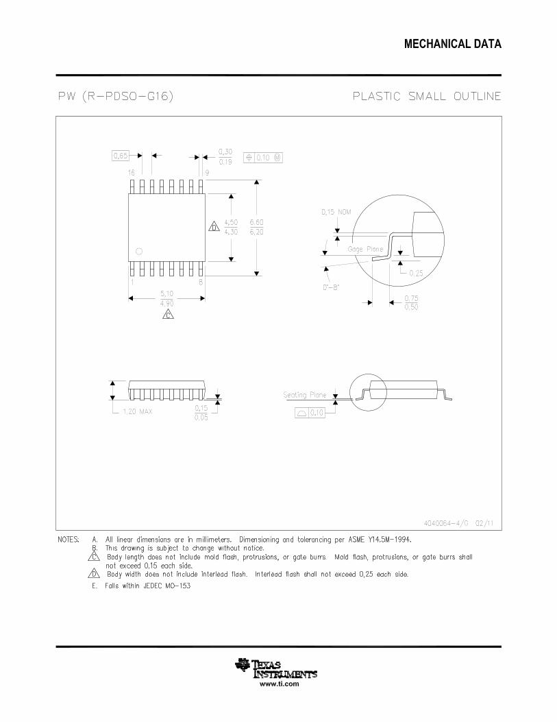
’LVDS391D OR PW PACKAGE
(TOP VIEW)
SN65LVDS387, SN75LVDS387, SN65LVDS389SN75LVDS389, SN65LVDS391, SN75LVDS391
www.ti.com SLLS362G –SEPTEMBER 1999–REVISED JANUARY 2016
5 Description (Continued)When disabled, the driver outputs are high-impedance. Each driver input (A) and enable (EN) have an internalpulldown that will drive the input to a low level when open-circuited.
The SN65LVDS387, SN65LVDS389, and SN65LVDS391 devices are characterized for operation from –40°C to85°C. The SN75LVDS387, SN75LVDS389, and SN75LVDS391 devices are characterized for operation from 0°Cto 70°C.
6 Device Options
PART NUMBER (1) TEMPERATURE RANGE NUMBER OF DRIVERS BUS-PIN ESDSN65LVDS387DGG –40°C to 85°C 16 15 kVSN75LVDS387DGG 0°C to 70°C 16 4 kVSN65LVDS389DBT –40°C to 85°C 8 15 kVSN75LVDS389DBT 0°C to 70°C 8 4 kVSN65LVDS391D –40°C to 85°C 4 15 kVSN75LVDS391D 0°C to 70°C 4 4 kVSN65LVDS391PW –40°C to 85°C 4 15 kVSN75LVDS391PW 0°C to 70°C 4 4 kV
(1) This package is available taped and reeled. To order this packaging option, add an R suffix to the partnumber (for example, SN65LVDS387DGGR).
7 Pin Configuration and Functions
Copyright © 1999–2016, Texas Instruments Incorporated Submit Documentation Feedback 3
Product Folder Links: SN65LVDS387 SN75LVDS387 SN65LVDS389 SN75LVDS389 SN65LVDS391 SN75LVDS391

SN65LVDS387, SN75LVDS387, SN65LVDS389SN75LVDS389, SN65LVDS391, SN75LVDS391SLLS362G –SEPTEMBER 1999–REVISED JANUARY 2016 www.ti.com
Pin Functions: SNx5LVDS391PIN
I/O DESCRIPTIONNAME NUMBER
VCC 4 – Supply voltageGND 5 – Ground1A 2 I LVTTL input signal1Y 16 O Differential (LVDS) non-inverting output1Z 15 O Differential (LVDS) inverting output2A 3 I LVTTL input signal2Y 14 O Differential (LVDS) non-inverting output2Z 13 O Differential (LVDS) inverting output3A 6 I LVTTL input signal3Y 12 O Differential (LVDS) non-inverting output3Z 11 O Differential (LVDS) inverting output4A 7 I LVTTL input signal4Y 10 O Differential (LVDS) non-inverting output4Z 9 O Differential (LVDS) inverting outputEN1,2 1 I Enable for channels 1 and 2EN3,4 8 I Enable for channels 3 and 4
Pin Functions: SNx5LVDS389PIN
I/O DESCRIPTIONNAME NUMBER
VCC 2, 10, 18 – Supply voltage1, 3, 9, 11,GND – Ground17, 19
A1A 5 I LVTTL input signalA1Y 38 O Differential (LVDS) non-inverting outputA1Z 37 O Differential (LVDS) inverting outputA2A 6 I LVTTL input signalA2Y 36 O Differential (LVDS) non-inverting outputA2Z 35 O Differential (LVDS) inverting outputA3A 7 I LVTTL input signalA3Y 34 O Differential (LVDS) non-inverting outputA3Z 33 O Differential (LVDS) inverting outputA4A 8 I LVTTL input signalA4Y 32 O Differential (LVDS) non-inverting outputA4Z 31 O Differential (LVDS) inverting outputB1A 12 I LVTTL input signalB1Y 27 O Differential (LVDS) non-inverting outputB1Z 26 O Differential (LVDS) inverting outputB2A 13 I LVTTL input signalB2Y 25 O Differential (LVDS) non-inverting outputB2Z 24 O Differential (LVDS) inverting outputB3A 14 I LVTTL input signalB3Y 23 O Differential (LVDS) non-inverting outputB3Z 22 O Differential (LVDS) inverting outputB4A 15 I LVTTL input signalB4Y 21 O Differential (LVDS) non-inverting outputB4B 20 O Differential (LVDS) inverting output
4 Submit Documentation Feedback Copyright © 1999–2016, Texas Instruments Incorporated
Product Folder Links: SN65LVDS387 SN75LVDS387 SN65LVDS389 SN75LVDS389 SN65LVDS391 SN75LVDS391
SN65LVDS387, SN75LVDS387, SN65LVDS389SN75LVDS389, SN65LVDS391, SN75LVDS391
www.ti.com SLLS362G –SEPTEMBER 1999–REVISED JANUARY 2016
Pin Functions: SNx5LVDS389 (continued)PIN
I/O DESCRIPTIONNAME NUMBER
ENA 4 I Enable for channel AENB 16 I Enable for channel BNC 28, 29, 30 – No connection
Pin Functions: SNx5LVDS387PIN
I/O DESCRIPTIONNAME NUMBER
2, 3, 16, 17,VCC – Supply voltage30, 311, 4, 15, 18,GND – Ground29, 32
A1A 6 I LVTTL input signalA1Y 64 O Differential (LVDS) non-inverting outputA1Z 73 O Differential (LVDS) inverting outputA2A 7 I LVTTL input signalA2Y 62 O Differential (LVDS) non-inverting outputA2Z 61 O Differential (LVDS) inverting outputA3A 8 I LVTTL input signalA3Y 60 O Differential (LVDS) non-inverting outputA3Z 59 O Differential (LVDS) inverting outputA4A 9 I LVTTL input signalA4Y 58 O Differential (LVDS) non-inverting outputA4Z 57 O Differential (LVDS) inverting outputB1A 11 I LVTTL input signalB1Y 56 O Differential (LVDS) non-inverting outputB1Z 55 O Differential (LVDS) inverting outputB2A 12 I LVTTL input signalB2Y 54 O Differential (LVDS) non-inverting outputB2Z 53 O Differential (LVDS) inverting outputB3A 13 I LVTTL input signalB3Y 52 O Differential (LVDS) non-inverting outputB3Z 51 O Differential (LVDS) inverting outputB4A 14 I LVTTL input signalB4Y 50 O Differential (LVDS) non-inverting outputB4B 49 O Differential (LVDS) inverting outputC1A 19 I LVTTL input signalC1Y 48 O Differential (LVDS) non-inverting outputC1Z 47 O Differential (LVDS) inverting outputC2A 20 I LVTTL input signalC2Y 46 O Differential (LVDS) non-inverting outputC2Z 45 O Differential (LVDS) inverting outputC3A 21 I LVTTL input signalC3Y 44 O Differential (LVDS) non-inverting outputC3Z 43 O Differential (LVDS) inverting outputC4A 22 I LVTTL input signalC4Y 42 O Differential (LVDS) non-inverting outputC4Z 41 O Differential (LVDS) inverting output
Copyright © 1999–2016, Texas Instruments Incorporated Submit Documentation Feedback 5
Product Folder Links: SN65LVDS387 SN75LVDS387 SN65LVDS389 SN75LVDS389 SN65LVDS391 SN75LVDS391

SN65LVDS387, SN75LVDS387, SN65LVDS389SN75LVDS389, SN65LVDS391, SN75LVDS391SLLS362G –SEPTEMBER 1999–REVISED JANUARY 2016 www.ti.com
Pin Functions: SNx5LVDS387 (continued)PIN
I/O DESCRIPTIONNAME NUMBER
D1A 24 I LVTTL input signalD1Y 40 O Differential (LVDS) non-inverting outputD1Z 39 O Differential (LVDS) inverting outputD2A 25 I LVTTL input signalD2Y 38 O Differential (LVDS) non-inverting outputD2Z 37 O Differential (LVDS) inverting outputD3A 26 I LVTTL input signalD3Y 36 O Differential (LVDS) non-inverting outputD3Z 35 O Differential (LVDS) inverting outputD4A 27 I LVTTL input signalD4Y 34 O Differential (LVDS) non-inverting outputB4B 33 O Differential (LVDS) inverting outputENA 5 I Enable for channel AENB 10 I Enable for channel BENC 23 I Enable for channel CEND 26 I Enable for channel D
8 Specifications
8.1 Absolute Maximum Ratingsover operating free-air temperature range (unless otherwise noted) (1)
MIN MAX UNITSupply voltage range, VCC
(2) –0.5 4 VInputs –0.5 6 V
Input voltage rangeY or Z –0.5 4 V
Continuous power dissipation See ThermalInformation
Lead temperature 1.6 mm (1/16 in) from case for 10 seconds 260 °CStorage temperature, Tstg –65 150 °C
(1) Stresses beyond those listed under Absolute Maximum Ratings may cause permanent damage to the device. These are stress ratingsonly, and functional operation of the device at these or any other conditions beyond those indicated under Recommended OperatingConditions is not implied. Exposure to absolute-maximum-rated conditions for extended periods may affect device reliability.
(2) All voltage values, except differential I/O bus voltages, are with respect to network ground pin.
8.2 ESD RatingsVALUE UNIT
Class 3, A ±15000 VSN65' (Y, Z, and GND)
Class 3, B ±400 VV(ESD) Electrostatic discharge
Class 3, A ±4000 VSN75' (Y, Z, and GND)
Class 3, B ±400 VLead temperature 1.6 mm (1/16 in) from case for 10 seconds 260 °C
6 Submit Documentation Feedback Copyright © 1999–2016, Texas Instruments Incorporated
Product Folder Links: SN65LVDS387 SN75LVDS387 SN65LVDS389 SN75LVDS389 SN65LVDS391 SN75LVDS391

SN65LVDS387, SN75LVDS387, SN65LVDS389SN75LVDS389, SN65LVDS391, SN75LVDS391
www.ti.com SLLS362G –SEPTEMBER 1999–REVISED JANUARY 2016
8.3 Recommended Operating ConditionsMIN NOM MAX UNIT
VCC Supply voltage 3 3.3 3.6 VVIH High-level input voltage 2 VVIL Low-level input voltage 0.8 V
SN75' 0 70 °COperating free-airTA temperature SN65' –40 85 °C
8.4 Thermal InformationSN65LVDS387 SN75LVDS387 SN65LVDS389SN75LVDS389 SN65LVDS391 SN75LVDS391
THERMAL METRIC (1) UNITDGG DBT D PW64 PINS 38 PINS 16 PINS 16 PINS
Derating Factor Above TA = 25°C (2) 16.7 8.5 7.6 6.2 mW/°CPower Rating: TA≤ 25°C 2094 1071 950 774Power Rating: TA = 70°C 1342 688 608 496 mWPower Rating: TA = 85°C 1089 556 494 402
(1) For more information about traditional and new thermal metrics, see the IC Package Thermal Metrics application report, SPRA953.(2) This is the inverse of the junction-to-ambient thermal resistance when board-mounted (low-k) and with no air flow.
8.5 Electrical Characteristicsover recommended operating conditions (unless otherwise noted)
PARAMETER TEST CONDITIONS MIN TYP (1) MAX UNIT|VOD| Differential output voltage magnitude 247 340 454
RL = 100 Ω, mVChange in differential output voltage See Figure 9 and Figure 10Δ|VOD| –50 50magnitude between logic statesSteady-state common-mode outputVOC(SS) 1.125 1.375 VvoltageChange in steady-state common-
ΔVOC(SS) mode output voltage between logic See Figure 11 –50 50 mVstatesPeak-to-peak common-mode outputVOC(PP) 50 150 mVvoltage
'LVDS387 85 95Enabled, RL = 100 Ω,'LVDS389 50 70VIN = 0.8 V or 2 V
'LVDS391 20 26ICC Supply current mA
'LVDS387 0.5 1.5Disabled,'LVDS389 0.5 1.5VIN = 0 V or VCC
'LVDS391 0.5 1.3IIH High-level input current VIH = 2 V 3 20 µAIIL Low-level input current VIL = 0.8 V 2 10 µA
VOY or VOZ = 0 V ±24 mAIOS Short-circuit output current
VOD = 0 V ±12 mAIOZ High-impedance output current VO = 0 V or VCC ±1 µAIO(OFF) Power-off output current VCC = 1.5 V, VO = 2.4 V ±1 µACIN Input capacitance VI = 0.4sin(4E6πt) + 0.5 V 5 pFCO Output capacitance VI = 0.4sin(4E6πt) + 0.5 V, Disabled 9.4 pF
(1) All typical values are at 25°C and with a 3.3-V supply.
Copyright © 1999–2016, Texas Instruments Incorporated Submit Documentation Feedback 7
Product Folder Links: SN65LVDS387 SN75LVDS387 SN65LVDS389 SN75LVDS389 SN65LVDS391 SN75LVDS391

SN65LVDS387, SN75LVDS387, SN65LVDS389SN75LVDS389, SN65LVDS391, SN75LVDS391SLLS362G –SEPTEMBER 1999–REVISED JANUARY 2016 www.ti.com
8.6 Switching Characteristicsover recommended operating conditions (unless otherwise noted)
PARAMETER TEST CONDITIONS MIN TYP (1) MAX UNITtPLH Propagation delay time, low-to-high-level output 0.9 1.7 2.9 nstPHL Propagation delay time, high-to-low-level output 0.9 1.6 2.9 nstr Differential output signal rise time 0.4 0.8 1 nsRL = 100 Ω,tf Differential output signal fall time CL = 10 pF, 0.4 0.8 1 ns
See Figure 12tsk(p) Pulse skew (|tPHL – tPLH|) 150 500 pstsk(o) Output skew (2) 80 150 pstsk(pp) Part-to-part skew (3) 1.5 ns
Propagation delay time, high-impedance-to-high-tPZH 6.4 15 nslevel outputPropagation delay time, high-impedance-to-low-tPZL 5.9 15 nslevel output
See Figure 13Propagation delay time, high-level-to-high-tPHZ 3.5 15 nsimpedance outputPropagation delay time, low-level-to-high-tPLZ 4.5 15 nsimpedance output
(1) All typical values are at 25°C and with a 3.3-V supply.(2) tsk(o) is the magnitude of the time difference between the tPLH or tPHL of all drivers of a single device with all of their inputs connected
together.(3) tsk(pp) is the magnitude of the difference in propagation delay times between any specified terminals of any two devices characterized in
this data sheet when both devices operate with the same supply voltage, at the same temperature, and have the same test circuits.
8 Submit Documentation Feedback Copyright © 1999–2016, Texas Instruments Incorporated
Product Folder Links: SN65LVDS387 SN75LVDS387 SN65LVDS389 SN75LVDS389 SN65LVDS391 SN75LVDS391
0
IOL − Low-Level Output Current − mA
4
3
04 6
2
2
VCC = 3.3 VTA = 25°C
1
VO
L−
Low
-Lev
el O
utpu
t Vol
tage
− V
Ta − Free-Air T emperature − °C
1.0
1.2
1.4
1.6
1.8
2.0
2.2
−40 −20 0 20 40 60 80 100
tP
HL
− H
igh-
To-
Low
Pro
paga
tion
Del
ay T
ime
− ns
VCC = 3.6 V
VCC = 3 V
VCC = 3.3 V
f − Frequency − MHz
− S
uppl
y C
urre
nt −
mA
IC
C
40
50
60
70
80
90
100
110
0 50 100 150 200 250 300
VCC = 3.6 V
All outputs loaded and enabled.
VCC = 3.3 V
VCC = 3 V
TA − Free-Air T emperature − °C
1.3
1.4
1.5
1.6
1.7
1.8
1.9
2.0
2.1
−40 −20 0 20 40 60 80 100
VCC = 3.6 V
VCC = 3 V
VCC = 3.3 V
tP
LH−
Low
-To-
Hig
h P
ropa
gatio
n D
elay
Tim
e −
ns
f − Frequency − MHz
− S
uppl
y C
urre
nt −
mA
IC
C
0
10
20
30
40
50
60
0 50 100 150 200 250 300
VCC = 3.6 V
All outputs loaded and enabled.
VCC = 3.3 V
VCC = 3 V
f − Frequency − MHz
− S
uppl
y C
urre
nt −
mA
IC
C
80
100
120
140
160
180
200
220
240
0 50 100 150 200 250 300 350
VCC = 3.6 V
All outputs loaded and enabled.
VCC = 3.3 V
VCC = 3 V
SN65LVDS387, SN75LVDS387, SN65LVDS389SN75LVDS389, SN65LVDS391, SN75LVDS391
www.ti.com SLLS362G –SEPTEMBER 1999–REVISED JANUARY 2016
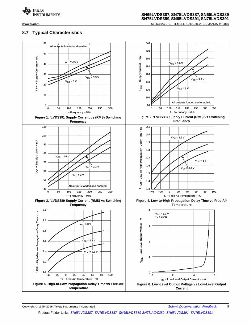
8.7 Typical Characteristics
Figure 2. 'LVDS387 Supply Current (RMS) vs SwitchingFigure 1. 'LVDS391 Supply Current vs (RMS) SwitchingFrequencyFrequency
Figure 3. 'LVDS389 Supply Current (RMS) vs Switching Figure 4. Low-to-High Propagation Delay Time vs Free-AirFrequency Temperature
Figure 5. High-to-Low Propagation Delay Time vs Free-Air Figure 6. Low-Level Output Voltage vs Low-Level OutputTemperature Current
Copyright © 1999–2016, Texas Instruments Incorporated Submit Documentation Feedback 9
Product Folder Links: SN65LVDS387 SN75LVDS387 SN65LVDS389 SN75LVDS389 SN65LVDS391 SN75LVDS391

−4
IOH − High-Level Output Current − mA
3.5
2.5
0−2 0
1.5
−3
0.5VO
H−
Hig
h-Le
vel O
utpu
t Vol
tage
− V
−1
3
2
1
VCC = 3.3 VTA = 25°C
t − Time − ns
− O
utpu
t Vol
tage
− V
VO
VOY
VOZ
VOD
SN65LVDS387, SN75LVDS387, SN65LVDS389SN75LVDS389, SN65LVDS391, SN75LVDS391SLLS362G –SEPTEMBER 1999–REVISED JANUARY 2016 www.ti.com
Typical Characteristics (continued)
Figure 8. Output Voltage vs TimeFigure 7. High-Level Output Voltage vs High-Level OutputCurrent
10 Submit Documentation Feedback Copyright © 1999–2016, Texas Instruments Incorporated
Product Folder Links: SN65LVDS387 SN75LVDS387 SN65LVDS389 SN75LVDS389 SN65LVDS391 SN75LVDS391

Y
ZInput
50 pF
49.9 Ω ± 1% (2 Places)
VOC
VO
VOC(PP) VOC(SS)
0 V
3 V
VI
±
3.75 kΩ
0 V ≤ VTEST ≤ 2.4 V
Y
ZVODInput 100 Ω
3.75 kΩ
GNDVI
A
(VOY + VOZ)/2
IOZ
IOYY
ZVOD
VOYVOC
II
VOZ
SN65LVDS387, SN75LVDS387, SN65LVDS389SN75LVDS389, SN65LVDS391, SN75LVDS391
www.ti.com SLLS362G –SEPTEMBER 1999–REVISED JANUARY 2016
9 Parameter Measurement Information
Figure 9. Voltage and Current Definitions
Figure 10. VOD Test Circuit
NOTE: All input pulses are supplied by a generator having the following characteristics: tr or tf ≤ 1 ns, pulse repetition rate(PRR) = 0.5 Mpps, pulse width = 500 ± 10 ns. CL includes instrumentation and fixture capacitance within 0.06 m ofthe device under test. The measurement of VOC(PP) is made on test equipment with a –3 dB bandwidth of at least 300MHz.
Figure 11. Test Circuit and Definitions for the Driver Common-Mode Output Voltage
Copyright © 1999–2016, Texas Instruments Incorporated Submit Documentation Feedback 11
Product Folder Links: SN65LVDS387 SN75LVDS387 SN65LVDS389 SN75LVDS389 SN65LVDS391 SN75LVDS391

CL = 10 pF(2 Places)
Y
Z
Input
49.9 Ω ± 1% (2 Places)
tPZH tPHZ
tPZL tPLZ
2 V1.4 V0.8 V
≅ 1.4 V1.3 V1.2 V
≅ 1 V
1.2 V1.1 V
Input
VOYor
VOZ
VOZor
VOY
VOY VOZ
0.8 V or 2 V
1.2 V+
–
Y
ZVOD
Input
CL = 10 pF(2 Places)
100 Ω ± 1 %
2 V1.4 V0.8 V
tPLH tPHL
100%80%
20%0%
Input
Output
0 V
tf tr
VOD(H)
VOD(L)
SN65LVDS387, SN75LVDS387, SN65LVDS389SN75LVDS389, SN65LVDS391, SN75LVDS391SLLS362G –SEPTEMBER 1999–REVISED JANUARY 2016 www.ti.com
Parameter Measurement Information (continued)
NOTE: All input pulses are supplied by a generator having the following characteristics: tr or tf ≤ 1 ns, pulse repetition rate(PRR) = 50 Mpps, pulse width = 10 ± 0.2 ns. CL includes instrumentation and fixture capacitance within 0.06 m of thedevice under test.
Figure 12. Test Circuit, Timing, and Voltage Definitions for the Differential Output Signal
NOTE: All input pulses are supplied by a generator having the following characteristics: tr or tf ≤ 1 ns, pulse repetition rate(PRR) = 0.5 Mpps, pulse width = 500 ± 10 ns. CL includes instrumentation and fixture capacitance within 0.06 m ofthe device under test.
Figure 13. Enable and Disable Time Circuit and Definitions
12 Submit Documentation Feedback Copyright © 1999–2016, Texas Instruments Incorporated
Product Folder Links: SN65LVDS387 SN75LVDS387 SN65LVDS389 SN75LVDS389 SN65LVDS391 SN75LVDS391

4Z
4Y
3Z
3Y
2Z
2Y
1Z
1Y
4A
3A
2A
1A
(1/4 of ’LVDS387 or 1/2 of ’LVDS389 shown)
EN
4Z
4Y
3Z
3Y
2Z
2Y
1Z
1Y
4A
3A
2A
1A
(’LVDS391 shown)
EN
EN
SN65LVDS387, SN75LVDS387, SN65LVDS389SN75LVDS389, SN65LVDS391, SN75LVDS391
www.ti.com SLLS362G –SEPTEMBER 1999–REVISED JANUARY 2016
10 Detailed Description
10.1 OverviewThe SNx5LVDSxx devices are quad-, eight-, and 16-channel LVDS line drivers. They operate from a singlesupply that is nominally 3.3 V, but can be as low as 3 V and as high as 3.6 V. The input signals to theSNx5LVDSxx device are LVTTL signals. The outputs of the device are differential signals complying with theLVDS standard (TIA/EIA-644A). The differential output signal operates with a signal level of 340 mV, nominally,at a common-mode voltage of 1.2 V. This low differential output voltage results in a low emitted radiated energy,which is dependent on the signal slew rate. The differential nature of the output provides immunity to common-mode coupled signals.
The SNx5LVDSxx device is intended to drive a 100-Ω transmission line. This transmission line may be a printed-circuit board (PCB) or cabled interconnect. With transmission lines, the optimum signal quality and powerdelivery is reached when the transmission line is terminated with a load equal to the characteristic impedance ofthe interconnect. Likewise, the driven 100-Ω transmission line should be terminated with a matched resistance.
10.2 Functional Block Diagram
Figure 14. Logic Diagram (Positive Logic)
10.3 Feature Description
10.3.1 Driver Output Voltage and Power-On ResetThe SNx5LVDSxx driver operates and meets all the specified performance requirements for supply voltages inthe range of 3.0 V to 3.6 V. When the supply voltage drops below 1.5 V (or is turning on and has not yet reached1.5 V), power-on reset circuitry sets the driver output to a high-impedance state.
10.3.2 5-V Input Tolerance5-V and 3.3-V TTL logic standards share the same input high-voltage and input low-voltage thresholds, namely2.0 V and 0.8 V, respectively. Although the maximum supply voltage for the SNx5LVDSxx is 3.6 V, the driver canoperate and meet all performance requirements when the input signals are as high as 5 V. This allows operationwith 3.3-V TTL as well as 5-V TTL logic. 3.3-V CMOS and 5-V CMOS inputs are also allowable, although oneshould ensure that the duty-cycle distortion that will result from the TTL (ground-referenced) thresholds areacceptable.
10.3.3 NC PinsNC (not connected) pins are pins where the die is not physically connected to the lead frame or package. Foroptimum thermal performance, a good rule of thumb is to ground the NC pins at the board level.
10.3.4 Unused Enable PinsUnused enable pins should be tied to VCC or GND as appropriate.
Copyright © 1999–2016, Texas Instruments Incorporated Submit Documentation Feedback 13
Product Folder Links: SN65LVDS387 SN75LVDS387 SN65LVDS389 SN75LVDS389 SN65LVDS391 SN75LVDS391

7 V
300 kΩ
50 Ω
VCC
A or ENInput
VCC
5 Ω
7 V
Y or ZOutput
EQUIVALENT OF EACH A OR EN INPUT TYPICAL OF ALL OUTPUTS
10 kΩ
SN65LVDS387, SN75LVDS387, SN65LVDS389SN75LVDS389, SN65LVDS391, SN75LVDS391SLLS362G –SEPTEMBER 1999–REVISED JANUARY 2016 www.ti.com
Feature Description (continued)10.3.5 Driver Equivalent SchematicsThe SNx5LVDSxx equivalent output schematic diagrams are shown in Figure 15. The driver input is representedby a CMOS inverter stage with a 7-V Zener diode. The input stage is high-impedance, and includes an internalpulldown to ground. If the driver input is left open, the driver input provides a low-level signal to the rest of thedriver circuitry, resulting in a low-level signal at the driver output pins. The Zener diode provides ESD protection.The driver output stage is a differential pair, one half of which is shown in Figure 15. Like the input stage, thedriver output includes Zener diodes for ESD protection. The schematic shows an output stage that includes a setof current sources (nominally 3.5 mA) that are connected to the output load circuit based upon the input stagesignal. To the first order, the SNx5LVDSxx output stage acts a constant-current source.
Figure 15. Equivalent Input and Output Schematic Diagrams
10.4 Device Functional ModesTable 1 provides the truth table for the SNx5LVDSxx devices.
Table 1. Driver Function Table (1)
INPUT ENABLE OUTPUTSA EN Y ZH H H LL H L HX L Z Z
OPEN H L H
(1) H = high-level, L = low-level, X = irrelevant, Z = high-impedance (off)
14 Submit Documentation Feedback Copyright © 1999–2016, Texas Instruments Incorporated
Product Folder Links: SN65LVDS387 SN75LVDS387 SN65LVDS389 SN75LVDS389 SN65LVDS391 SN75LVDS391

SN65LVDS387, SN75LVDS387, SN65LVDS389SN75LVDS389, SN65LVDS391, SN75LVDS391
www.ti.com SLLS362G –SEPTEMBER 1999–REVISED JANUARY 2016
11 Application and Implementation
NOTEInformation in the following applications sections is not part of the TI componentspecification, and TI does not warrant its accuracy or completeness. TI’s customers areresponsible for determining suitability of components for their purposes. Customers shouldvalidate and test their design implementation to confirm system functionality.
11.1 Application InformationThe intended application of this device and signaling technique is for point-to-point and multidrop baseband datatransmission over controlled impedance media of approximately 100 Ω. The transmission media can be printed-circuit board traces, backplanes, or cables. The large number of drivers integrated into the same substrate, alongwith the low pulse skew of balanced signaling, allows extremely precise timing alignment of clock and data forsynchronous parallel data transfers. When used with the companion 16- or 8-channel receivers, theSN65LVDS386 or SN65LVDS388, over 200 million data transfers per second in single-edge clocked systems arepossible with very little power.
NOTEThe ultimate rate and distance of data transfer is dependent upon the attenuationcharacteristics of the media, the noise coupling to the environment, and other systemcharacteristics.
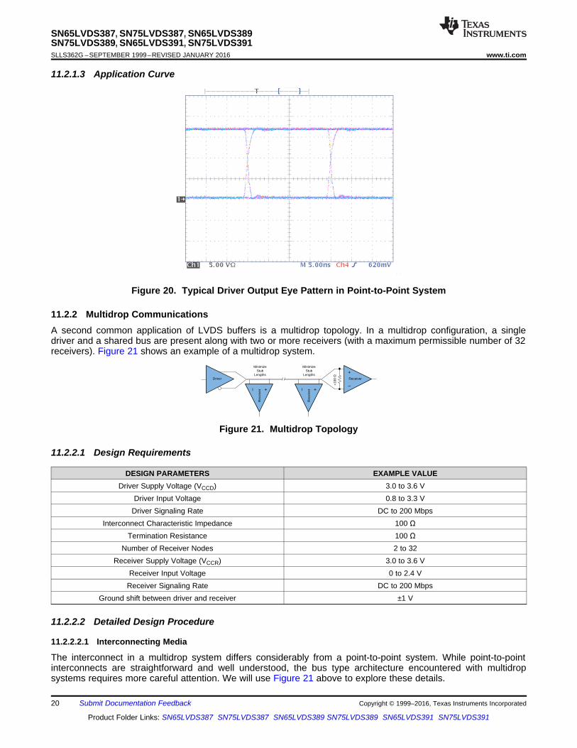
11.1.1 Signaling Rate vs DistanceThe ultimate data transfer rate over a given cable or trace length involves many variables. Starting with thecapabilities of this LVDS driver to reproduce a data pulse as short as 1.6 ns (a 630-Mbps signaling rate) with lessthan 500 ps of pulse distortion, any degradation of this pulse by the transmission media will necessarily reducethe timing margin at the receiving end of the data link.
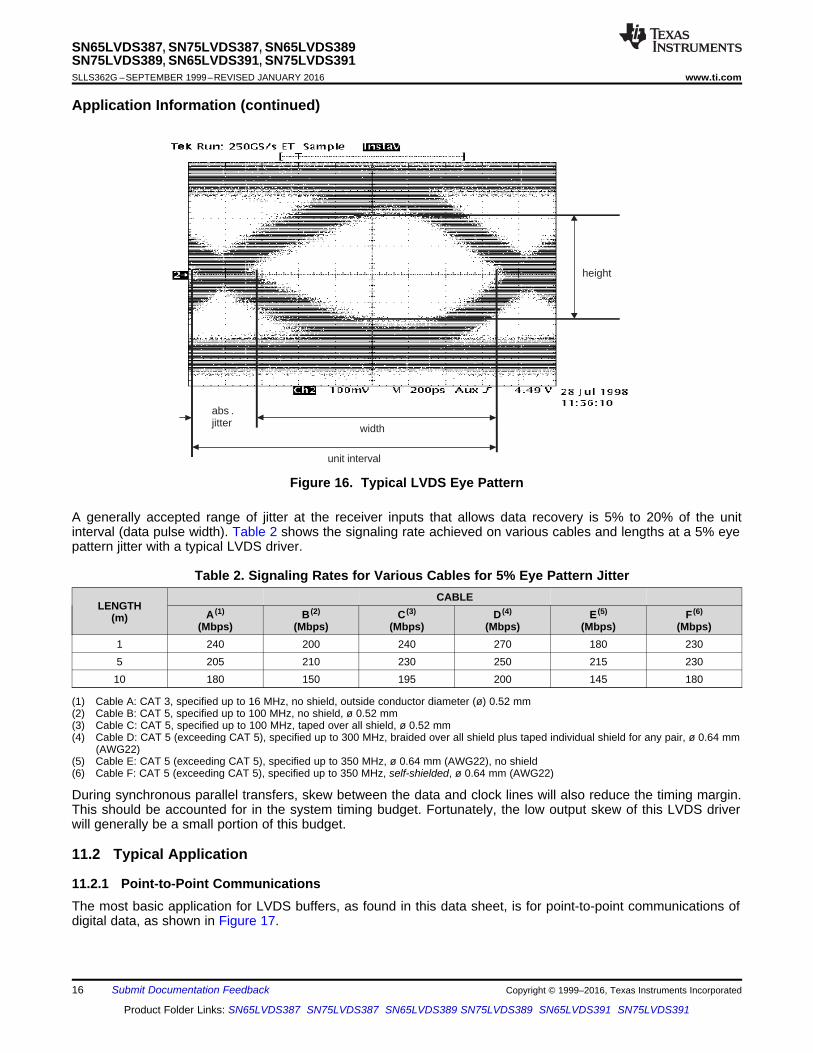
The timing uncertainty induced by the transmission media is commonly referred to as jitter and comes fromnumerous sources. The characteristics of a particular transmission media can be quantified by using an eyepattern measurement such as shown in Figure 16, which shows about 340 ps of jitter or 20% of the data pulsewidth.
Copyright © 1999–2016, Texas Instruments Incorporated Submit Documentation Feedback 15
Product Folder Links: SN65LVDS387 SN75LVDS387 SN65LVDS389 SN75LVDS389 SN65LVDS391 SN75LVDS391
width
abs .jitter
height
unit interval
SN65LVDS387, SN75LVDS387, SN65LVDS389SN75LVDS389, SN65LVDS391, SN75LVDS391SLLS362G –SEPTEMBER 1999–REVISED JANUARY 2016 www.ti.com
Application Information (continued)
Figure 16. Typical LVDS Eye Pattern
A generally accepted range of jitter at the receiver inputs that allows data recovery is 5% to 20% of the unitinterval (data pulse width). Table 2 shows the signaling rate achieved on various cables and lengths at a 5% eyepattern jitter with a typical LVDS driver.
Table 2. Signaling Rates for Various Cables for 5% Eye Pattern JitterCABLE
LENGTHA (1) B (2) C (3) D (4) E (5) F (6)
(m)(Mbps) (Mbps) (Mbps) (Mbps) (Mbps) (Mbps)
1 240 200 240 270 180 2305 205 210 230 250 215 23010 180 150 195 200 145 180
(1) Cable A: CAT 3, specified up to 16 MHz, no shield, outside conductor diameter (ø) 0.52 mm(2) Cable B: CAT 5, specified up to 100 MHz, no shield, ø 0.52 mm(3) Cable C: CAT 5, specified up to 100 MHz, taped over all shield, ø 0.52 mm(4) Cable D: CAT 5 (exceeding CAT 5), specified up to 300 MHz, braided over all shield plus taped individual shield for any pair, ø 0.64 mm
(AWG22)(5) Cable E: CAT 5 (exceeding CAT 5), specified up to 350 MHz, ø 0.64 mm (AWG22), no shield(6) Cable F: CAT 5 (exceeding CAT 5), specified up to 350 MHz, self-shielded, ø 0.64 mm (AWG22)
During synchronous parallel transfers, skew between the data and clock lines will also reduce the timing margin.This should be accounted for in the system timing budget. Fortunately, the low output skew of this LVDS driverwill generally be a small portion of this budget.
11.2 Typical Application
11.2.1 Point-to-Point CommunicationsThe most basic application for LVDS buffers, as found in this data sheet, is for point-to-point communications ofdigital data, as shown in Figure 17.
16 Submit Documentation Feedback Copyright © 1999–2016, Texas Instruments Incorporated
Product Folder Links: SN65LVDS387 SN75LVDS387 SN65LVDS389 SN75LVDS389 SN65LVDS391 SN75LVDS391

Driver 100 Receiver
IN+
IN-
OUT+
OUT-
SN65LVDS387, SN75LVDS387, SN65LVDS389SN75LVDS389, SN65LVDS391, SN75LVDS391
www.ti.com SLLS362G –SEPTEMBER 1999–REVISED JANUARY 2016
Typical Application (continued)
Figure 17. Point-to-Point Topology
A point-to-point communications channel has a single transmitter (driver) and a single receiver. Thiscommunications topology is often referred to as simplex. In Figure 17 the driver receives a single-ended inputsignal and the receiver outputs a single-ended recovered signal. The LVDS driver converts the single-endedinput to a differential signal for transmission over a balanced interconnecting media of 100-Ω characteristicimpedance. The conversion from a single-ended signal to an LVDS signal retains the digital data payload whiletranslating to a signal whose features are more appropriate for communication over extended distances or in anoisy environment.
11.2.1.1 Design Requirements
DESIGN PARAMETERS EXAMPLE VALUEDriver Supply Voltage (VCCD) 3.0 to 3.6 V
Driver Input Voltage 0.8 to 3.3 VDriver Signaling Rate DC to 200 Mbps
Interconnect Characteristic Impedance 100 ΩTermination Resistance 100 Ω
Number of Receiver Nodes 1Receiver Supply Voltage (VCCR) 3.0 to 3.6 V
Receiver Input Voltage 0 to 2.4 VReceiver Signaling Rate DC to 200 Mbps
Ground shift between driver and receiver ±1 V
11.2.1.2 Detailed Design Procedure
11.2.1.2.1 Driver Supply Voltage
The SNx5LVDSxx driver is operated from a single supply. The device can support operation with a supply as lowas 3 V and as high as 3.6 V. The differential output voltage is nominally 340 mV over the complete output range.The minimum output voltage stays within the specified LVDS limits (247 mV to 454 mV) for the complete 3-V to3.6-V supply range.
11.2.1.2.2 Driver Bypass Capacitance
Bypass capacitors play a key role in power distribution circuitry. Specifically, they create low-impedance pathsbetween power and ground. At low frequencies, a good digital power supply offers very-low-impedance pathsbetween its terminals. However, as higher frequency currents propagate through power traces, the source isquite often incapable of maintaining a low-impedance path to ground. Bypass capacitors are used to address thisshortcoming. Usually, large bypass capacitors (10 μF to 1000 μF) at the board-level do a good job up into thekHz range. Due to their size and length of their leads, they tend to have large inductance values at the switchingfrequencies of modern digital circuitry. To solve this problem, one should resort to the use of smaller capacitors(nF to μF range) installed locally next to the integrated circuit.
Multilayer ceramic chip or surface-mount capacitors (size 0603 or 0805) minimize lead inductances of bypasscapacitors in high-speed environments, because their lead inductance is about 1 nH. For comparison purposes,a typical capacitor with leads has a lead inductance around 5 nH.
Copyright © 1999–2016, Texas Instruments Incorporated Submit Documentation Feedback 17
Product Folder Links: SN65LVDS387 SN75LVDS387 SN65LVDS389 SN75LVDS389 SN65LVDS391 SN75LVDS391
0.1 µF 0.001 µF
3.3 V
LVDS1A
C 200 ps 0.001 F0.2V
æ ö= ´ = mç ÷
è ø
Maximum Step Change Supply Currentchip Rise Time
Maximum Power Supply Noise
IC T
V
Dæ ö= ´ç ÷Dè ø
SN65LVDS387, SN75LVDS387, SN65LVDS389SN75LVDS389, SN65LVDS391, SN75LVDS391SLLS362G –SEPTEMBER 1999–REVISED JANUARY 2016 www.ti.com
The value of the bypass capacitors used locally with LVDS chips can be determined by the following formulaaccording to Johnson (1), equations 8.18 to 8.21. A conservative rise time of 200 ps and a worst-case change insupply current of 1 A covers the whole range of LVDS devices offered by Texas Instruments. In this example, themaximum power supply noise tolerated is 200 mV; however, this figure varies depending on the noise budgetavailable in your design. (1)
(1)
(2)
The following example lowers lead inductance and covers intermediate frequencies between the board-levelcapacitor (>10 µF) and the value of capacitance found above (0.001 µF). You should place the smallest value ofcapacitance as close as possible to the chip.
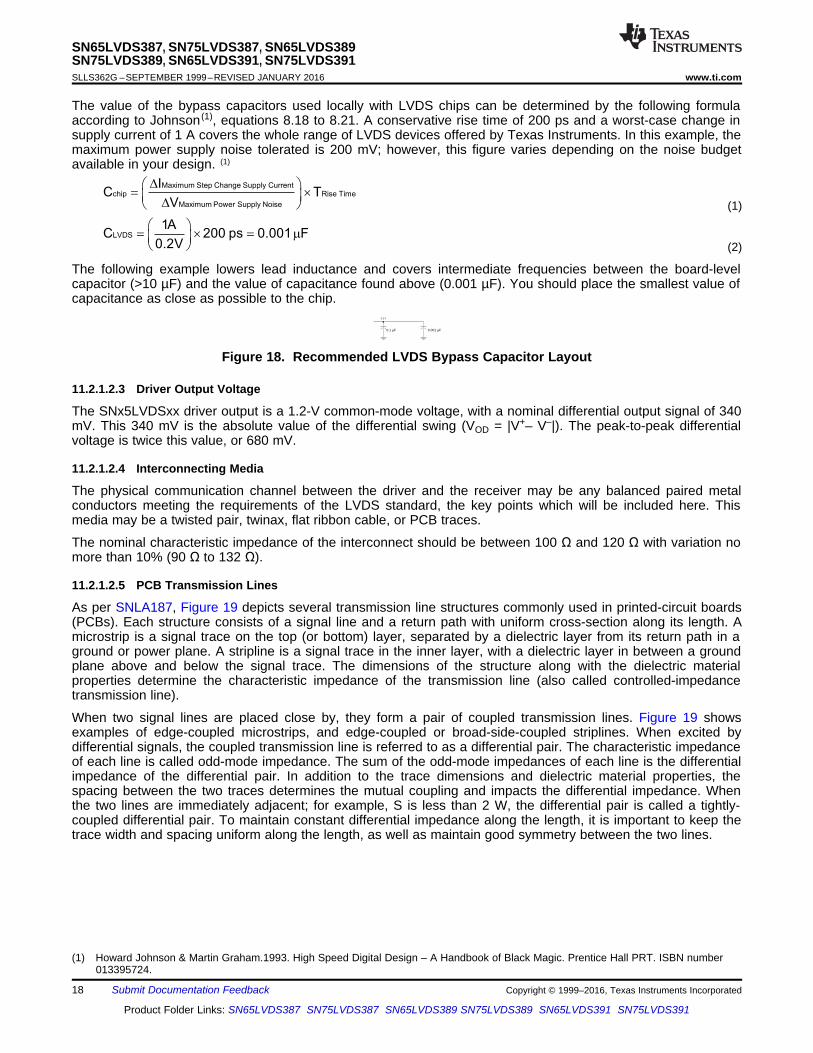
Figure 18. Recommended LVDS Bypass Capacitor Layout
11.2.1.2.3 Driver Output Voltage
The SNx5LVDSxx driver output is a 1.2-V common-mode voltage, with a nominal differential output signal of 340mV. This 340 mV is the absolute value of the differential swing (VOD = |V+– V–|). The peak-to-peak differentialvoltage is twice this value, or 680 mV.
11.2.1.2.4 Interconnecting Media
The physical communication channel between the driver and the receiver may be any balanced paired metalconductors meeting the requirements of the LVDS standard, the key points which will be included here. Thismedia may be a twisted pair, twinax, flat ribbon cable, or PCB traces.
The nominal characteristic impedance of the interconnect should be between 100 Ω and 120 Ω with variation nomore than 10% (90 Ω to 132 Ω).
11.2.1.2.5 PCB Transmission Lines
As per SNLA187, Figure 19 depicts several transmission line structures commonly used in printed-circuit boards(PCBs). Each structure consists of a signal line and a return path with uniform cross-section along its length. Amicrostrip is a signal trace on the top (or bottom) layer, separated by a dielectric layer from its return path in aground or power plane. A stripline is a signal trace in the inner layer, with a dielectric layer in between a groundplane above and below the signal trace. The dimensions of the structure along with the dielectric materialproperties determine the characteristic impedance of the transmission line (also called controlled-impedancetransmission line).
When two signal lines are placed close by, they form a pair of coupled transmission lines. Figure 19 showsexamples of edge-coupled microstrips, and edge-coupled or broad-side-coupled striplines. When excited bydifferential signals, the coupled transmission line is referred to as a differential pair. The characteristic impedanceof each line is called odd-mode impedance. The sum of the odd-mode impedances of each line is the differentialimpedance of the differential pair. In addition to the trace dimensions and dielectric material properties, thespacing between the two traces determines the mutual coupling and impacts the differential impedance. Whenthe two lines are immediately adjacent; for example, S is less than 2 W, the differential pair is called a tightly-coupled differential pair. To maintain constant differential impedance along the length, it is important to keep thetrace width and spacing uniform along the length, as well as maintain good symmetry between the two lines.
(1) Howard Johnson & Martin Graham.1993. High Speed Digital Design – A Handbook of Black Magic. Prentice Hall PRT. ISBN number013395724.
18 Submit Documentation Feedback Copyright © 1999–2016, Texas Instruments Incorporated
Product Folder Links: SN65LVDS387 SN75LVDS387 SN65LVDS389 SN75LVDS389 SN65LVDS391 SN75LVDS391

0r
87 5.98 HZ ln
0.8 W T1.41
§ · ¨ ¸H © ¹
> @> @0
r
1.9 2 H T60Z ln
0.8 W T
§ · ¨ ¸¨ ¸H © ¹
s0.96
Hdiff 0Z 2 Z 1 0.48 e
u§ ·¨ ¸ u u u¨ ¸© ¹
s2.9
Hdiff 0Z 2 Z 1 0.347e
u§ ·¨ ¸ u u ¨ ¸© ¹
Co-Planar Coupled Microstrips
Broad-Side Coupled Striplines
Edge-Coupled Edge-Coupled
Single-Ended Microstrip Single-Ended Stripline
W
H
T
W
TH
H
S
H
Differential Microstrip Differential Stripline
S
H
S
H
HG G
W W W
S
SN65LVDS387, SN75LVDS387, SN65LVDS389SN75LVDS389, SN65LVDS391, SN75LVDS391
www.ti.com SLLS362G –SEPTEMBER 1999–REVISED JANUARY 2016
Figure 19. Controlled-Impedance Transmission Lines
11.2.1.2.6 Termination Resistor
As shown earlier, an LVDS communication channel employs a current source driving a transmission line which isterminated with a resistive load. This load serves to convert the transmitted current into a voltage at the receiverinput. To ensure incident wave switching (which is necessary to operate the channel at the highest signalingrate), the termination resistance should be matched to the characteristic impedance of the transmission line. Thedesigner should ensure that the termination resistance is within 10% of the nominal media characteristicimpedance. If the transmission line is targeted for 100-Ω impedance, the termination resistance should bebetween 90 Ω and 110 Ω.
The line termination resistance should be located as close as possible to the receiver, thereby minimizing thestub length from the resistor to the receiver. The limiting case would be to incorporate the termination resistorinto the receiver, which is exactly what is offered with the TI ‘LVDT receivers.
While we talk in this section about point-to-point communications, a word of caution is useful when a multidroptopology is used. In such topologies, line termination resistors are to be located only at the end(s) of thetransmission line. In such an environment, LVDS receivers could be used for loads branching off the main buswith an LVDT receiver used only at the bus end.
11.2.1.2.7 Driver NC Pins
NC (not connected) pins are pins where the die is not physically connected to the lead frame or package. Foroptimum thermal performance, a good rule of thumb is to ground the NC pins at the board level.
Copyright © 1999–2016, Texas Instruments Incorporated Submit Documentation Feedback 19
Product Folder Links: SN65LVDS387 SN75LVDS387 SN65LVDS389 SN75LVDS389 SN65LVDS391 SN75LVDS391
Driver
+
±
|10
0
Receiver
MinimizeStub
Lengths
MinimizeStub
Lengths
+±
Rec
eive
r +±
Rec
eive
r
SN65LVDS387, SN75LVDS387, SN65LVDS389SN75LVDS389, SN65LVDS391, SN75LVDS391SLLS362G –SEPTEMBER 1999–REVISED JANUARY 2016 www.ti.com
11.2.1.3 Application Curve
Figure 20. Typical Driver Output Eye Pattern in Point-to-Point System
11.2.2 Multidrop CommunicationsA second common application of LVDS buffers is a multidrop topology. In a multidrop configuration, a singledriver and a shared bus are present along with two or more receivers (with a maximum permissible number of 32receivers). Figure 21 shows an example of a multidrop system.
Figure 21. Multidrop Topology
11.2.2.1 Design Requirements
DESIGN PARAMETERS EXAMPLE VALUEDriver Supply Voltage (VCCD) 3.0 to 3.6 V
Driver Input Voltage 0.8 to 3.3 VDriver Signaling Rate DC to 200 Mbps
Interconnect Characteristic Impedance 100 ΩTermination Resistance 100 Ω
Number of Receiver Nodes 2 to 32Receiver Supply Voltage (VCCR) 3.0 to 3.6 V
Receiver Input Voltage 0 to 2.4 VReceiver Signaling Rate DC to 200 Mbps
Ground shift between driver and receiver ±1 V
11.2.2.2 Detailed Design Procedure
11.2.2.2.1 Interconnecting Media
The interconnect in a multidrop system differs considerably from a point-to-point system. While point-to-pointinterconnects are straightforward and well understood, the bus type architecture encountered with multidropsystems requires more careful attention. We will use Figure 21 above to explore these details.
20 Submit Documentation Feedback Copyright © 1999–2016, Texas Instruments Incorporated
Product Folder Links: SN65LVDS387 SN75LVDS387 SN65LVDS389 SN75LVDS389 SN65LVDS391 SN75LVDS391

SN65LVDS387, SN75LVDS387, SN65LVDS389SN75LVDS389, SN65LVDS391, SN75LVDS391
www.ti.com SLLS362G –SEPTEMBER 1999–REVISED JANUARY 2016
The most basic multidrop system would include a single driver, located at a bus origin, with multiple receivernodes branching off the main line, and a final receiver at the end of the transmission line, co-located with a bustermination resistor. While this would be the most basic multidrop system, it has several considerations not yetexplored.
The location of the transmitter at one bus end allows the design concerns to be simplified, but this comes at thecost of flexibility. With a transmitter located at the origin, a single bus termination at the far-end is required. Thefar-end termination absorbs the incident traveling wave. The flexibility lost with this arrangement is thus: if thesingle transmitter needed to be relocated on the bus, at any location other than the origin, we would be facedwith a bus with one open-circuited end, and one properly terminated end. Locating the transmitter say in themiddle of the bus may be desired to reduce (by ½) the maximum flight time from the transmitter to receiver.
Another new feature in Figure 21 is clear in that every node branching off the main line results in stubs. Thestubs should be minimized in any case, but have the unintended effect of locally changing the loaded impedanceof the bus.
To a good approximation, the characteristic transmission line impedance seen into any cut point in the unloadedmultipoint or multidrop bus is defined by √L/C, where L is the inductance per unit length and C is the capacitanceper unit length. As capacitance is added to the bus in the form of devices and interconnections, the buscharacteristic impedance is lowered. This may result in signal reflections from the impedance mismatch betweenthe unloaded and loaded segments of the bus.
If the number of loads is constant and can be distributed evenly along the line, reflections can be reduced bychanging the bus termination resistors to match the loaded characteristic impedance. Normally, the number ofloads are not constant or distributed evenly and the reflections resulting from any mismatching should beaccounted for in the noise budget.
11.2.2.3 Application Curve
Figure 22. Typical Driver Output Eye Pattern in Multidrop System
Copyright © 1999–2016, Texas Instruments Incorporated Submit Documentation Feedback 21
Product Folder Links: SN65LVDS387 SN75LVDS387 SN65LVDS389 SN75LVDS389 SN65LVDS391 SN75LVDS391

SN65LVDS387, SN75LVDS387, SN65LVDS389SN75LVDS389, SN65LVDS391, SN75LVDS391SLLS362G –SEPTEMBER 1999–REVISED JANUARY 2016 www.ti.com
12 Power Supply Recommendations
The LVDS driver and receivers in this data sheet are designed to operate from a single power supply. Bothdrivers and receivers operate with supply voltages in the range of 2.4 V to 3.6 V. In a typical application, a driverand a receiver may be on separate boards, or even separate equipment. In these cases, separate supplieswould be used at each location. The expected ground potential difference between the driver power supply andthe receiver power supply would be less than |±1 V|. Board-level and local device-level bypass capacitanceshould be used and are covered in Driver Bypass Capacitance.
13 Layout
13.1 Layout Guidelines
13.1.1 Microstrip vs Stripline TopologiesAs per SLLD009, printed-circuit boards usually offer designers two transmission line options: Microstrip andstripline. Microstrips are traces on the outer layer of a PCB, as shown in Figure 23.
Figure 23. Microstrip Topology
On the other hand, striplines are traces between two ground planes. Striplines are less prone to emissions andsusceptibility problems because the reference planes effectively shield the embedded traces. However, from thestandpoint of high-speed transmission, juxtaposing two planes creates additional capacitance. TI recommendsrouting LVDS signals on microstrip transmission lines, if possible. The PCB traces allow designers to specify thenecessary tolerances for ZO based on the overall noise budget and reflection allowances. Footnotes 1 (1), 2 (2),and 3 (3) provide formulas for ZO and tPD for differential and single-ended traces. (1) (2) (3)
Figure 24. Stripline Topology
13.1.2 Dielectric Type and Board ConstructionThe speeds at which signals travel across the board dictates the choice of dielectric. FR-4, or equivalent, usuallyprovides adequate performance for use with LVDS signals. If rise or fall times of TTL/CMOS signals are lessthan 500 ps, empirical results indicate that a material with a dielectric constant near 3.4, such as Rogers™ 4350or Nelco N4000-13 is better suited. Once the designer chooses the dielectric, there are several parameterspertaining to the board construction that can affect performance. The following set of guidelines were developedexperimentally through several designs involving LVDS devices:• Copper weight: 15 g or 1/2 oz start, plated to 30 g or 1 oz• All exposed circuitry should be solder-plated (60/40) to 7.62 μm or 0.0003 in (minimum).• Copper plating should be 25.4 μm or 0.001 in (minimum) in plated-through-holes.• Solder mask over bare copper with solder hot-air leveling
(1) Howard Johnson & Martin Graham.1993. High Speed Digital Design – A Handbook of Black Magic. Prentice Hall PRT. ISBN number013395724.
(2) Mark I. Montrose. 1996. Printed Circuit Board Design Techniques for EMC Compliance. IEEE Press. ISBN number 0780311310.(3) Clyde F. Coombs, Jr. Ed, Printed Circuits Handbook, McGraw Hill, ISBN number 0070127549.
22 Submit Documentation Feedback Copyright © 1999–2016, Texas Instruments Incorporated
Product Folder Links: SN65LVDS387 SN75LVDS387 SN65LVDS389 SN75LVDS389 SN65LVDS391 SN75LVDS391

t2 W
W
W
W
Minimum spacing asdefined by PCB vendor
LVDSPair
TTL/CMOSTrace
Differential Traces
Single-Ended Traces
S =
Layer 4: Routed Plane (TTL Signals)
Layer 3: Power Plane
Layer 2: Ground Plane
Layer 1: Routed Plane (LVDS Signals)
Layer 4: Ground Plane
Layer 5: Ground Plane
Layer 4: Routed Plane (TTL/CMOS Signals)
Layer 3: Power Plane
Layer 2: Ground Plane
Layer 1: Routed Plane (LVDS Signals)
SN65LVDS387, SN75LVDS387, SN65LVDS389SN75LVDS389, SN65LVDS391, SN75LVDS391
www.ti.com SLLS362G –SEPTEMBER 1999–REVISED JANUARY 2016
Layout Guidelines (continued)13.1.3 Recommended Stack LayoutFollowing the choice of dielectrics and design specifications, you should decide how many levels to use in thestack. To reduce the TTL/CMOS to LVDS crosstalk, it is a good practice to have at least two separate signalplanes as shown in Figure 25.
Figure 25. Four-Layer PCB Board
NOTEThe separation between layers 2 and 3 should be 127 μm (0.005 in). By keeping thepower and ground planes tightly coupled, the increased capacitance acts as a bypass fortransients.
One of the most common stack configurations is the six-layer board, as shown in Figure 26.
Figure 26. Six-Layer PCB Board
In this particular configuration, it is possible to isolate each signal layer from the power plane by at least oneground plane. The result is improved signal integrity; however, fabrication is more expensive. Using the 6-layerboard is preferable, because it offers the layout designer more flexibility in varying the distance between signallayers and referenced planes, in addition to ensuring reference to a ground plane for signal layers 1 and 6.
13.1.4 Separation Between TracesThe separation between traces depends on several factors; however, the amount of coupling that can betolerated usually dictates the actual separation. Low-noise coupling requires close coupling between thedifferential pair of an LVDS link to benefit from the electromagnetic field cancellation. The traces should be 100-Ωdifferential and thus coupled in the manner that best fits this requirement. In addition, differential pairs shouldhave the same electrical length to ensure that they are balanced, thus minimizing problems with skew and signalreflection.
In the case of two adjacent single-ended traces, one should use the 3-W rule, which stipulates that the distancebetween two traces should be greater than two times the width of a single trace, or three times its widthmeasured from trace center to trace center. This increased separation effectively reduces the potential forcrosstalk. The same rule should be applied to the separation between adjacent LVDS differential pairs, whetherthe traces are edge-coupled or broad-side-coupled.
Figure 27. 3-W Rule for Single-Ended and Differential Traces (Top View)
Copyright © 1999–2016, Texas Instruments Incorporated Submit Documentation Feedback 23
Product Folder Links: SN65LVDS387 SN75LVDS387 SN65LVDS389 SN75LVDS389 SN65LVDS391 SN75LVDS391

Signal Trace
Uninterrupted Ground Plane
Signal Trace
Uninterrupted Ground Plane
Signal Via
Ground Via
Layer 6
Layer 1
SN65LVDS387, SN75LVDS387, SN65LVDS389SN75LVDS389, SN65LVDS391, SN75LVDS391SLLS362G –SEPTEMBER 1999–REVISED JANUARY 2016 www.ti.com
Layout Guidelines (continued)You should exercise caution when using autorouters, because they do not always account for all factors affectingcrosstalk and signal reflection. For instance, it is best to avoid sharp 90° turns to prevent discontinuities in thesignal path. Using successive 45° turns tends to minimize reflections.
13.1.5 Crosstalk and Ground Bounce MinimizationTo reduce crosstalk, it is important to provide a return path to high-frequency currents that is as close as possibleto its originating trace. A ground plane usually achieves this. Because the returning currents always choose thepath of lowest inductance, they are most likely to return directly under the original trace, thus minimizingcrosstalk. Lowering the area of the current loop lowers the potential for crosstalk. Traces kept as short aspossible with an uninterrupted ground plane running beneath them emit the minimum amount of electromagneticfield strength. Discontinuities in the ground plane increase the return path inductance and should be avoided.
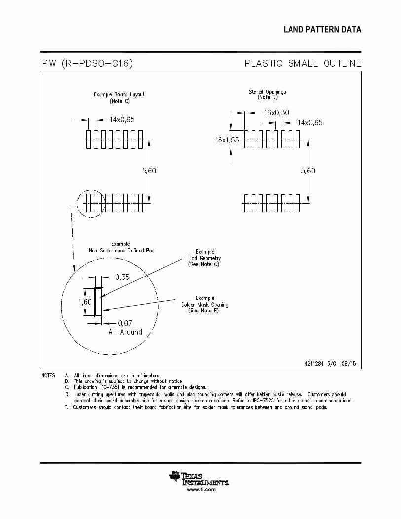
13.2 Layout ExampleAt least two or three times the width of an individual trace should separate single-ended traces and differentialpairs to minimize the potential for crosstalk. Single-ended traces that run in parallel for less than the wavelengthof the rise or fall times usually have negligible crosstalk. Increase the spacing between signal paths for longparallel runs to reduce crosstalk. Boards with limited real estate can benefit from the staggered trace layout, asshown in Figure 28.
Figure 28. Staggered Trace Layout
This configuration lays out alternating signal traces on different layers; thus, the horizontal separation betweentraces can be less than 2 or 3 times the width of individual traces. To ensure continuity in the ground signal path,TI recommends having an adjacent ground via for every signal via, as shown in Figure 29. Note that vias createadditional capacitance. For example, a typical via has a lumped capacitance effect of 1/2 pF to 1 pF in FR4.
Figure 29. Ground Via Location (Side View)
Short and low-impedance connection of the device ground pins to the PCB ground plane reduces groundbounce. Holes and cutouts in the ground planes can adversely affect current return paths if they creatediscontinuities that increase returning current loop areas.
To minimize EMI problems, TI recommends avoiding discontinuities below a trace (for example, holes, slits, andso on) and keeping traces as short as possible. Zoning the board wisely by placing all similar functions in thesame area, as opposed to mixing them together, helps reduce susceptibility issues.
24 Submit Documentation Feedback Copyright © 1999–2016, Texas Instruments Incorporated
Product Folder Links: SN65LVDS387 SN75LVDS387 SN65LVDS389 SN75LVDS389 SN65LVDS391 SN75LVDS391

SN65LVDS387, SN75LVDS387, SN65LVDS389SN75LVDS389, SN65LVDS391, SN75LVDS391
www.ti.com SLLS362G –SEPTEMBER 1999–REVISED JANUARY 2016
14 Device and Documentation Support
14.1 Device Support
14.1.1 Third-Party Products DisclaimerTI'S PUBLICATION OF INFORMATION REGARDING THIRD-PARTY PRODUCTS OR SERVICES DOES NOTCONSTITUTE AN ENDORSEMENT REGARDING THE SUITABILITY OF SUCH PRODUCTS OR SERVICESOR A WARRANTY, REPRESENTATION OR ENDORSEMENT OF SUCH PRODUCTS OR SERVICES, EITHERALONE OR IN COMBINATION WITH ANY TI PRODUCT OR SERVICE.
14.1.2 Other LVDS ProductsFor other products and application notes in the LVDS and LVDM product families visit our Web site athttp://www.ti.com/sc/datatran.
14.2 Documentation Support
14.2.1 Related InformationIBIS modeling is available for this device. Contact the local TI sales office or the TI Web site at www.ti.com formore information.
For more application guidelines, see the following documents:• Low-Voltage Differential Signaling Design Notes (SLLA014)• Interface Circuits for TIA/EIA-644 (LVDS) (SLLA038)• Reducing EMI With LVDS (SLLA030)• Slew Rate Control of LVDS Circuits (SLLA034)• Using an LVDS Receiver With RS-422 Data (SLLA031)• Evaluating the LVDS EVM (SLLA033)
14.3 Related LinksTable 3 lists quick access links. Categories include technical documents, support and community resources,tools and software, and quick access to sample or buy.
Table 3. Related LinksTECHNICAL TOOLS & SUPPORT &PARTS PRODUCT FOLDER SAMPLE & BUY DOCUMENTS SOFTWARE COMMUNITY
SN65LVDS387 Click here Click here Click here Click here Click hereSN75LVDS387 Click here Click here Click here Click here Click hereSN65LVDS389 Click here Click here Click here Click here Click hereSN75LVDS389 Click here Click here Click here Click here Click hereSN65LVDS391 Click here Click here Click here Click here Click hereSN75LVDS391 Click here Click here Click here Click here Click here
14.4 TrademarksRogers is a trademark of Rogers Corporation.All other trademarks are the property of their respective owners.
14.5 Electrostatic Discharge CautionThese devices have limited built-in ESD protection. The leads should be shorted together or the device placed in conductive foamduring storage or handling to prevent electrostatic damage to the MOS gates.
Copyright © 1999–2016, Texas Instruments Incorporated Submit Documentation Feedback 25
Product Folder Links: SN65LVDS387 SN75LVDS387 SN65LVDS389 SN75LVDS389 SN65LVDS391 SN75LVDS391
SN65LVDS387, SN75LVDS387, SN65LVDS389SN75LVDS389, SN65LVDS391, SN75LVDS391SLLS362G –SEPTEMBER 1999–REVISED JANUARY 2016 www.ti.com
14.6 GlossarySLYZ022 — TI Glossary.
This glossary lists and explains terms, acronyms, and definitions.
15 Mechanical, Packaging, and Orderable InformationThe following pages include mechanical, packaging, and orderable information. This information is the mostcurrent data available for the designated devices. This data is subject to change without notice and revision ofthis document. For browser-based versions of this data sheet, refer to the left-hand navigation.
26 Submit Documentation Feedback Copyright © 1999–2016, Texas Instruments Incorporated
Product Folder Links: SN65LVDS387 SN75LVDS387 SN65LVDS389 SN75LVDS389 SN65LVDS391 SN75LVDS391
PACKAGE OPTION ADDENDUM
www.ti.com 14-Jan-2016
Addendum-Page 1
PACKAGING INFORMATION
Orderable Device Status(1)
Package Type PackageDrawing
Pins PackageQty
Eco Plan(2)
Lead/Ball Finish(6)
MSL Peak Temp(3)
Op Temp (°C) Device Marking(4/5)
Samples
SN65LVDS387DGG ACTIVE TSSOP DGG 64 25 Green (RoHS& no Sb/Br)
CU NIPDAU Level-2-260C-1 YEAR -40 to 85 LVDS387
SN65LVDS387DGGG4 ACTIVE TSSOP DGG 64 25 Green (RoHS& no Sb/Br)
CU NIPDAU Level-2-260C-1 YEAR -40 to 85 LVDS387
SN65LVDS387DGGR ACTIVE TSSOP DGG 64 2000 Green (RoHS& no Sb/Br)
CU NIPDAU Level-2-260C-1 YEAR -40 to 85 LVDS387
SN65LVDS387DGGRG4 ACTIVE TSSOP DGG 64 2000 Green (RoHS& no Sb/Br)
CU NIPDAU Level-2-260C-1 YEAR -40 to 85 LVDS387
SN65LVDS389DBT ACTIVE TSSOP DBT 38 50 Green (RoHS& no Sb/Br)
CU NIPDAU Level-2-260C-1 YEAR -40 to 85 LVDS389
SN65LVDS389DBTG4 ACTIVE TSSOP DBT 38 50 Green (RoHS& no Sb/Br)
CU NIPDAU Level-2-260C-1 YEAR -40 to 85 LVDS389
SN65LVDS389DBTR ACTIVE TSSOP DBT 38 2000 Green (RoHS& no Sb/Br)
CU NIPDAU Level-2-260C-1 YEAR -40 to 85 LVDS389
SN65LVDS391D ACTIVE SOIC D 16 40 Green (RoHS& no Sb/Br)
CU NIPDAU Level-1-260C-UNLIM -40 to 85 LVDS391
SN65LVDS391DG4 ACTIVE SOIC D 16 40 Green (RoHS& no Sb/Br)
CU NIPDAU Level-1-260C-UNLIM -40 to 85 LVDS391
SN65LVDS391DR ACTIVE SOIC D 16 2500 Green (RoHS& no Sb/Br)
CU NIPDAU Level-1-260C-UNLIM -40 to 85 LVDS391
SN65LVDS391DRG4 ACTIVE SOIC D 16 2500 Green (RoHS& no Sb/Br)
CU NIPDAU Level-1-260C-UNLIM -40 to 85 LVDS391
SN65LVDS391PW ACTIVE TSSOP PW 16 90 Green (RoHS& no Sb/Br)
CU NIPDAU Level-1-260C-UNLIM -40 to 85 LVDS391
SN65LVDS391PWG4 ACTIVE TSSOP PW 16 90 Green (RoHS& no Sb/Br)
CU NIPDAU Level-1-260C-UNLIM -40 to 85 LVDS391
SN65LVDS391PWR ACTIVE TSSOP PW 16 2000 Green (RoHS& no Sb/Br)
CU NIPDAU Level-1-260C-UNLIM -40 to 85 LVDS391
SN65LVDS391PWRG4 ACTIVE TSSOP PW 16 2000 Green (RoHS& no Sb/Br)
CU NIPDAU Level-1-260C-UNLIM -40 to 85 LVDS391
SN75LVDS387DGG ACTIVE TSSOP DGG 64 25 Green (RoHS& no Sb/Br)
CU NIPDAU Level-2-260C-1 YEAR 0 to 70 75LVDS387
SN75LVDS387DGGG4 ACTIVE TSSOP DGG 64 25 Green (RoHS& no Sb/Br)
CU NIPDAU Level-2-260C-1 YEAR 0 to 70 75LVDS387

PACKAGE OPTION ADDENDUM
www.ti.com 14-Jan-2016
Addendum-Page 2
Orderable Device Status(1)
Package Type PackageDrawing
Pins PackageQty
Eco Plan(2)
Lead/Ball Finish(6)
MSL Peak Temp(3)
Op Temp (°C) Device Marking(4/5)
Samples
SN75LVDS387DGGR ACTIVE TSSOP DGG 64 2000 Green (RoHS& no Sb/Br)
CU NIPDAU Level-2-260C-1 YEAR 0 to 70 75LVDS387
SN75LVDS387DGGRG4 ACTIVE TSSOP DGG 64 2000 Green (RoHS& no Sb/Br)
CU NIPDAU Level-2-260C-1 YEAR 0 to 70 75LVDS387
SN75LVDS389DBT ACTIVE TSSOP DBT 38 50 Green (RoHS& no Sb/Br)
CU NIPDAU Level-2-260C-1 YEAR 0 to 70 75LVDS389
SN75LVDS389DBTG4 ACTIVE TSSOP DBT 38 50 Green (RoHS& no Sb/Br)
CU NIPDAU Level-2-260C-1 YEAR 0 to 70 75LVDS389
SN75LVDS389DBTR ACTIVE TSSOP DBT 38 2000 Green (RoHS& no Sb/Br)
CU NIPDAU Level-2-260C-1 YEAR 0 to 70 75LVDS389
SN75LVDS389DBTRG4 ACTIVE TSSOP DBT 38 2000 Green (RoHS& no Sb/Br)
CU NIPDAU Level-2-260C-1 YEAR 0 to 70 75LVDS389
SN75LVDS391D ACTIVE SOIC D 16 40 Green (RoHS& no Sb/Br)
CU NIPDAU Level-1-260C-UNLIM 0 to 70 75LVDS391
SN75LVDS391DG4 ACTIVE SOIC D 16 40 Green (RoHS& no Sb/Br)
CU NIPDAU Level-1-260C-UNLIM 0 to 70 75LVDS391
SN75LVDS391DR ACTIVE SOIC D 16 2500 Green (RoHS& no Sb/Br)
CU NIPDAU Level-1-260C-UNLIM 0 to 70 75LVDS391
SN75LVDS391PW ACTIVE TSSOP PW 16 90 Green (RoHS& no Sb/Br)
CU NIPDAU Level-1-260C-UNLIM 0 to 70 DS391
SN75LVDS391PWG4 ACTIVE TSSOP PW 16 90 Green (RoHS& no Sb/Br)
CU NIPDAU Level-1-260C-UNLIM 0 to 70 DS391
SN75LVDS391PWR ACTIVE TSSOP PW 16 2000 Green (RoHS& no Sb/Br)
CU NIPDAU Level-1-260C-UNLIM 0 to 70 DS391
SN75LVDS391PWRG4 ACTIVE TSSOP PW 16 2000 Green (RoHS& no Sb/Br)
CU NIPDAU Level-1-260C-UNLIM 0 to 70 DS391
(1) The marketing status values are defined as follows:ACTIVE: Product device recommended for new designs.LIFEBUY: TI has announced that the device will be discontinued, and a lifetime-buy period is in effect.NRND: Not recommended for new designs. Device is in production to support existing customers, but TI does not recommend using this part in a new design.PREVIEW: Device has been announced but is not in production. Samples may or may not be available.OBSOLETE: TI has discontinued the production of the device.
(2) Eco Plan - The planned eco-friendly classification: Pb-Free (RoHS), Pb-Free (RoHS Exempt), or Green (RoHS & no Sb/Br) - please check http://www.ti.com/productcontent for the latest availabilityinformation and additional product content details.TBD: The Pb-Free/Green conversion plan has not been defined.

PACKAGE OPTION ADDENDUM
www.ti.com 14-Jan-2016
Addendum-Page 3
Pb-Free (RoHS): TI's terms "Lead-Free" or "Pb-Free" mean semiconductor products that are compatible with the current RoHS requirements for all 6 substances, including the requirement thatlead not exceed 0.1% by weight in homogeneous materials. Where designed to be soldered at high temperatures, TI Pb-Free products are suitable for use in specified lead-free processes.Pb-Free (RoHS Exempt): This component has a RoHS exemption for either 1) lead-based flip-chip solder bumps used between the die and package, or 2) lead-based die adhesive used betweenthe die and leadframe. The component is otherwise considered Pb-Free (RoHS compatible) as defined above.Green (RoHS & no Sb/Br): TI defines "Green" to mean Pb-Free (RoHS compatible), and free of Bromine (Br) and Antimony (Sb) based flame retardants (Br or Sb do not exceed 0.1% by weightin homogeneous material)
(3) MSL, Peak Temp. - The Moisture Sensitivity Level rating according to the JEDEC industry standard classifications, and peak solder temperature.
(4) There may be additional marking, which relates to the logo, the lot trace code information, or the environmental category on the device.
(5) Multiple Device Markings will be inside parentheses. Only one Device Marking contained in parentheses and separated by a "~" will appear on a device. If a line is indented then it is a continuationof the previous line and the two combined represent the entire Device Marking for that device.
(6) Lead/Ball Finish - Orderable Devices may have multiple material finish options. Finish options are separated by a vertical ruled line. Lead/Ball Finish values may wrap to two lines if the finishvalue exceeds the maximum column width.
Important Information and Disclaimer:The information provided on this page represents TI's knowledge and belief as of the date that it is provided. TI bases its knowledge and belief on informationprovided by third parties, and makes no representation or warranty as to the accuracy of such information. Efforts are underway to better integrate information from third parties. TI has taken andcontinues to take reasonable steps to provide representative and accurate information but may not have conducted destructive testing or chemical analysis on incoming materials and chemicals.TI and TI suppliers consider certain information to be proprietary, and thus CAS numbers and other limited information may not be available for release.
In no event shall TI's liability arising out of such information exceed the total purchase price of the TI part(s) at issue in this document sold by TI to Customer on an annual basis.

TAPE AND REEL INFORMATION
*All dimensions are nominal
Device PackageType
PackageDrawing
Pins SPQ ReelDiameter
(mm)
ReelWidth
W1 (mm)
A0(mm)
B0(mm)
K0(mm)
P1(mm)
W(mm)
Pin1Quadrant
SN65LVDS387DGGR TSSOP DGG 64 2000 330.0 24.4 8.4 17.3 1.7 12.0 24.0 Q1
SN65LVDS389DBTR TSSOP DBT 38 2000 330.0 16.4 6.9 10.2 1.8 12.0 16.0 Q1
SN65LVDS391DR SOIC D 16 2500 330.0 16.4 6.5 10.3 2.1 8.0 16.0 Q1
SN65LVDS391PWR TSSOP PW 16 2000 330.0 12.4 6.9 5.6 1.6 8.0 12.0 Q1
SN75LVDS387DGGR TSSOP DGG 64 2000 330.0 24.4 8.4 17.3 1.7 12.0 24.0 Q1
SN75LVDS389DBTR TSSOP DBT 38 2000 330.0 16.4 6.9 10.2 1.8 12.0 16.0 Q1
SN75LVDS391DR SOIC D 16 2500 330.0 16.4 6.5 10.3 2.1 8.0 16.0 Q1
SN75LVDS391PWR TSSOP PW 16 2000 330.0 12.4 6.9 5.6 1.6 8.0 12.0 Q1
PACKAGE MATERIALS INFORMATION
www.ti.com 24-Aug-2016
Pack Materials-Page 1

*All dimensions are nominal
Device Package Type Package Drawing Pins SPQ Length (mm) Width (mm) Height (mm)
SN65LVDS387DGGR TSSOP DGG 64 2000 367.0 367.0 45.0
SN65LVDS389DBTR TSSOP DBT 38 2000 367.0 367.0 38.0
SN65LVDS391DR SOIC D 16 2500 367.0 367.0 38.0
SN65LVDS391PWR TSSOP PW 16 2000 367.0 367.0 38.0
SN75LVDS387DGGR TSSOP DGG 64 2000 367.0 367.0 45.0
SN75LVDS389DBTR TSSOP DBT 38 2000 367.0 367.0 38.0
SN75LVDS391DR SOIC D 16 2500 367.0 367.0 38.0
SN75LVDS391PWR TSSOP PW 16 2000 367.0 367.0 38.0
PACKAGE MATERIALS INFORMATION
www.ti.com 24-Aug-2016
Pack Materials-Page 2


MECHANICAL DATA
MTSS003D – JANUARY 1995 – REVISED JANUARY 1998
POST OFFICE BOX 655303 • DALLAS, TEXAS 75265
DGG (R-PDSO-G**) PLASTIC SMALL-OUTLINE PACKAGE
4040078/F 12/97
48 PINS SHOWN
0,25
0,15 NOM
Gage Plane
6,006,20 8,30
7,90
0,750,50
Seating Plane
25
0,270,17
24
A
48
1
1,20 MAX
M0,08
0,10
0,50
0°–8°
56
14,10
13,90
48DIM
A MAX
A MIN
PINS **
12,40
12,60
64
17,10
16,90
0,150,05
NOTES: A. All linear dimensions are in millimeters.B. This drawing is subject to change without notice.C. Body dimensions do not include mold protrusion not to exceed 0,15.D. Falls within JEDEC MO-153

IMPORTANT NOTICE
Texas Instruments Incorporated and its subsidiaries (TI) reserve the right to make corrections, enhancements, improvements and otherchanges to its semiconductor products and services per JESD46, latest issue, and to discontinue any product or service per JESD48, latestissue. Buyers should obtain the latest relevant information before placing orders and should verify that such information is current andcomplete. All semiconductor products (also referred to herein as “components”) are sold subject to TI’s terms and conditions of salesupplied at the time of order acknowledgment.TI warrants performance of its components to the specifications applicable at the time of sale, in accordance with the warranty in TI’s termsand conditions of sale of semiconductor products. Testing and other quality control techniques are used to the extent TI deems necessaryto support this warranty. Except where mandated by applicable law, testing of all parameters of each component is not necessarilyperformed.TI assumes no liability for applications assistance or the design of Buyers’ products. Buyers are responsible for their products andapplications using TI components. To minimize the risks associated with Buyers’ products and applications, Buyers should provideadequate design and operating safeguards.TI does not warrant or represent that any license, either express or implied, is granted under any patent right, copyright, mask work right, orother intellectual property right relating to any combination, machine, or process in which TI components or services are used. Informationpublished by TI regarding third-party products or services does not constitute a license to use such products or services or a warranty orendorsement thereof. Use of such information may require a license from a third party under the patents or other intellectual property of thethird party, or a license from TI under the patents or other intellectual property of TI.Reproduction of significant portions of TI information in TI data books or data sheets is permissible only if reproduction is without alterationand is accompanied by all associated warranties, conditions, limitations, and notices. TI is not responsible or liable for such altereddocumentation. Information of third parties may be subject to additional restrictions.Resale of TI components or services with statements different from or beyond the parameters stated by TI for that component or servicevoids all express and any implied warranties for the associated TI component or service and is an unfair and deceptive business practice.TI is not responsible or liable for any such statements.Buyer acknowledges and agrees that it is solely responsible for compliance with all legal, regulatory and safety-related requirementsconcerning its products, and any use of TI components in its applications, notwithstanding any applications-related information or supportthat may be provided by TI. Buyer represents and agrees that it has all the necessary expertise to create and implement safeguards whichanticipate dangerous consequences of failures, monitor failures and their consequences, lessen the likelihood of failures that might causeharm and take appropriate remedial actions. Buyer will fully indemnify TI and its representatives against any damages arising out of the useof any TI components in safety-critical applications.In some cases, TI components may be promoted specifically to facilitate safety-related applications. With such components, TI’s goal is tohelp enable customers to design and create their own end-product solutions that meet applicable functional safety standards andrequirements. Nonetheless, such components are subject to these terms.No TI components are authorized for use in FDA Class III (or similar life-critical medical equipment) unless authorized officers of the partieshave executed a special agreement specifically governing such use.Only those TI components which TI has specifically designated as military grade or “enhanced plastic” are designed and intended for use inmilitary/aerospace applications or environments. Buyer acknowledges and agrees that any military or aerospace use of TI componentswhich have not been so designated is solely at the Buyer's risk, and that Buyer is solely responsible for compliance with all legal andregulatory requirements in connection with such use.TI has specifically designated certain components as meeting ISO/TS16949 requirements, mainly for automotive use. In any case of use ofnon-designated products, TI will not be responsible for any failure to meet ISO/TS16949.
Products ApplicationsAudio www.ti.com/audio Automotive and Transportation www.ti.com/automotiveAmplifiers amplifier.ti.com Communications and Telecom www.ti.com/communicationsData Converters dataconverter.ti.com Computers and Peripherals www.ti.com/computersDLP® Products www.dlp.com Consumer Electronics www.ti.com/consumer-appsDSP dsp.ti.com Energy and Lighting www.ti.com/energyClocks and Timers www.ti.com/clocks Industrial www.ti.com/industrialInterface interface.ti.com Medical www.ti.com/medicalLogic logic.ti.com Security www.ti.com/securityPower Mgmt power.ti.com Space, Avionics and Defense www.ti.com/space-avionics-defenseMicrocontrollers microcontroller.ti.com Video and Imaging www.ti.com/videoRFID www.ti-rfid.comOMAP Applications Processors www.ti.com/omap TI E2E Community e2e.ti.comWireless Connectivity www.ti.com/wirelessconnectivity
Mailing Address: Texas Instruments, Post Office Box 655303, Dallas, Texas 75265Copyright © 2016, Texas Instruments Incorporated