sns foil development program - neutron sciences · • foil corrugation method developed 10 m 20 mm...
TRANSCRIPT
SNS Foil Development Program
Robert Shaw
Chemical Sciences Division
February 24-26, 2009
SNS ASAC Review 2009
Co-authors: Mike Plum, Chris Luck, SNS
L. Wilson, ORNL, and C.S. Feigerle (UT/K)

OAK RIDGE NATIONAL LABORATORY
U. S. DEPARTMENT OF ENERGY2SNS ASAC Review, February 24-26, 2009
Outline
Foil requirements for the SNS.
Corrugated, nanocrystalline diamond foils.
Alpha ranging for foil thickness determination.
Diamond foil performance at SNS and PSR.
30 keV electron beam foil test stand.
New directions.
OAK RIDGE NATIONAL LABORATORY
U. S. DEPARTMENT OF ENERGY3SNS ASAC Review, February 24-26, 2009
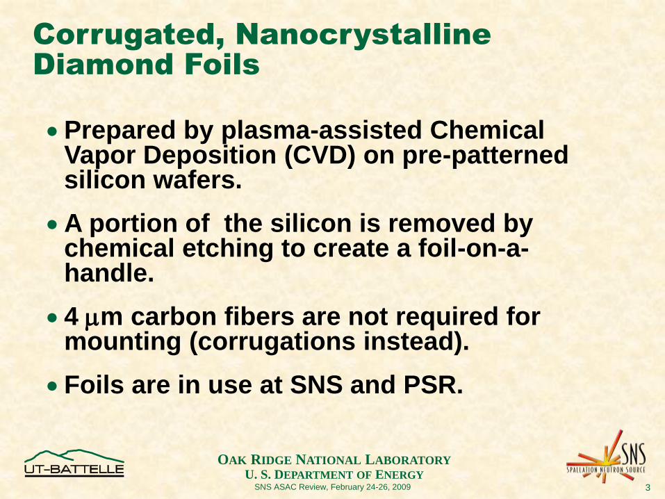
Corrugated, Nanocrystalline
Diamond Foils
Prepared by plasma-assisted Chemical Vapor Deposition (CVD) on pre-patterned silicon wafers.
A portion of the silicon is removed by chemical etching to create a foil-on-a-handle.
4 m carbon fibers are not required for mounting (corrugations instead).
Foils are in use at SNS and PSR.

OAK RIDGE NATIONAL LABORATORY
U. S. DEPARTMENT OF ENERGY4SNS ASAC Review, February 24-26, 2009
SNS Foil Requirements
H- from linac
H+ from ring H+ to ring
e- to collector
• Withstand peak temperatures up to 2500 K ???
• Stripping efficiency of 97% (of intercepted beam)
• Foil set of 11 foils must last 90 day cycle --> 200 hr each
• 20 mm x 12 mm (25 x 17) freestanding foil, single edge support
• Uniform thickness of 280 g/cm2 (~0.8 m for diamond)
OAK RIDGE NATIONAL LABORATORY
U. S. DEPARTMENT OF ENERGY5SNS ASAC Review, February 24-26, 2009
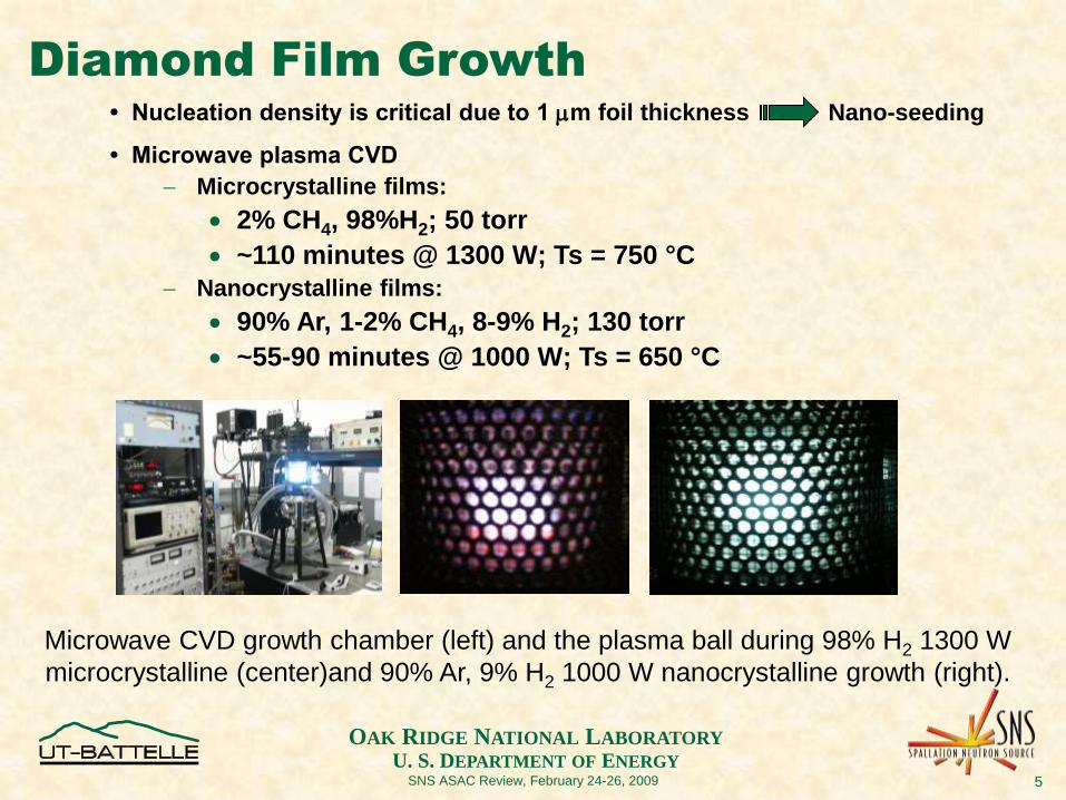
Diamond Film Growth
• Nucleation density is critical due to 1 m foil thickness
• Microwave plasma CVD
Microcrystalline films:
2% CH4, 98%H2; 50 torr
~110 minutes @ 1300 W; Ts = 750 °C
Nanocrystalline films:
90% Ar, 1-2% CH4, 8-9% H2; 130 torr
~55-90 minutes @ 1000 W; Ts = 650 °C
Microwave CVD growth chamber (left) and the plasma ball during 98% H2 1300 W
microcrystalline (center)and 90% Ar, 9% H2 1000 W nanocrystalline growth (right).
Nano-seeding

OAK RIDGE NATIONAL LABORATORY
U. S. DEPARTMENT OF ENERGY6SNS ASAC Review, February 24-26, 2009
Corrugated Diamond Foils for
Flatness
• Thermal expansion mismatch
diamond vs silicon
• Foils scroll upon release from Si wafer
• Foil corrugation method developed
10 m 20
mm
50 Line/inch Foil:254 m
10 m
Develop with ultraviolet light
Etch with Buffered Oxide Etch
Strip resist with Acetone
Etch Silicon with TMAH
Strip oxide with Buffered Oxide Etch
Positive PhotoresistSiO2
Silicon Substrate
Patterning Process
12 mm

OAK RIDGE NATIONAL LABORATORY
U. S. DEPARTMENT OF ENERGY7SNS ASAC Review, February 24-26, 2009
Corrugated foils avoid the need for
carbon fiber support
LANL/PSR Foil Mount
OAK RIDGE NATIONAL LABORATORY
U. S. DEPARTMENT OF ENERGY8SNS ASAC Review, February 24-26, 2009
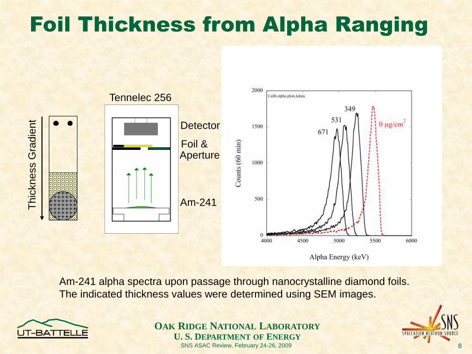
Foil Thickness from Alpha Ranging
Am-241 alpha spectra upon passage through nanocrystalline diamond foils.
The indicated thickness values were determined using SEM images.
Am-241
Aperture
Detector
Tennelec 256
Foil &
Thic
kness G
radie
nt

OAK RIDGE NATIONAL LABORATORY
U. S. DEPARTMENT OF ENERGY9SNS ASAC Review, February 24-26, 2009
Correlation between diamond foil thickness as determined using SEM images
and the energy shift of transmitted Am-241 alpha particles.
Foil Thickness Correlation
Thickness:
± 3% precision
OAK RIDGE NATIONAL LABORATORY
U. S. DEPARTMENT OF ENERGY10SNS ASAC Review, February 24-26, 2009
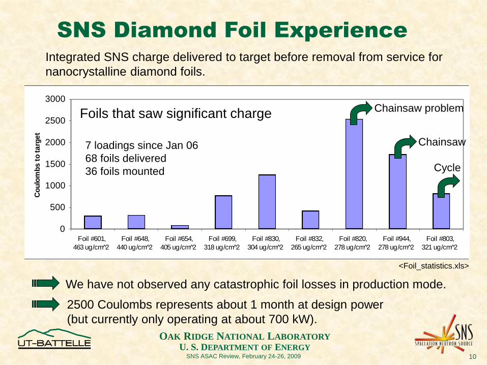
Integrated SNS charge delivered to target before removal from service for
nanocrystalline diamond foils.
SNS Diamond Foil Experience
0
500
1000
1500
2000
2500
3000
Foil #601,
463 ug/cm 2̂
Foil #648,
440 ug/cm 2̂
Foil #654,
405 ug/cm 2̂
Foil #699,
318 ug/cm 2̂
Foil #830,
304 ug/cm 2̂
Foil #832,
265 ug/cm 2̂
Foil #820,
278 ug/cm 2̂
Foil #944,
278 ug/cm 2̂
Foil #803,
321 ug/cm 2̂
Co
ulo
mb
s t
o ta
rge
t
<Foil_statistics.xls>
7 loadings since Jan 06
68 foils delivered
36 foils mounted
Foils that saw significant charge Chainsaw problem
Chainsaw
Cycle
We have not observed any catastrophic foil losses in production mode.
2500 Coulombs represents about 1 month at design power
(but currently only operating at about 700 kW).

OAK RIDGE NATIONAL LABORATORY
U. S. DEPARTMENT OF ENERGY11SNS ASAC Review, February 24-26, 2009
<601 looking upstream.jpg>
Photograph of a nanocrystalline SNS foil (#601; 463 ug/cm2 avg) after
experiencing 300 C of injected charge. The lower left corner is curled away from the
camera from interaction with the injected and circulating ion beam.

OAK RIDGE NATIONAL LABORATORY
U. S. DEPARTMENT OF ENERGY12SNS ASAC Review, February 24-26, 2009
SNS Foil 699 after 783 C
OAK RIDGE NATIONAL LABORATORY
U. S. DEPARTMENT OF ENERGY13SNS ASAC Review, February 24-26, 2009
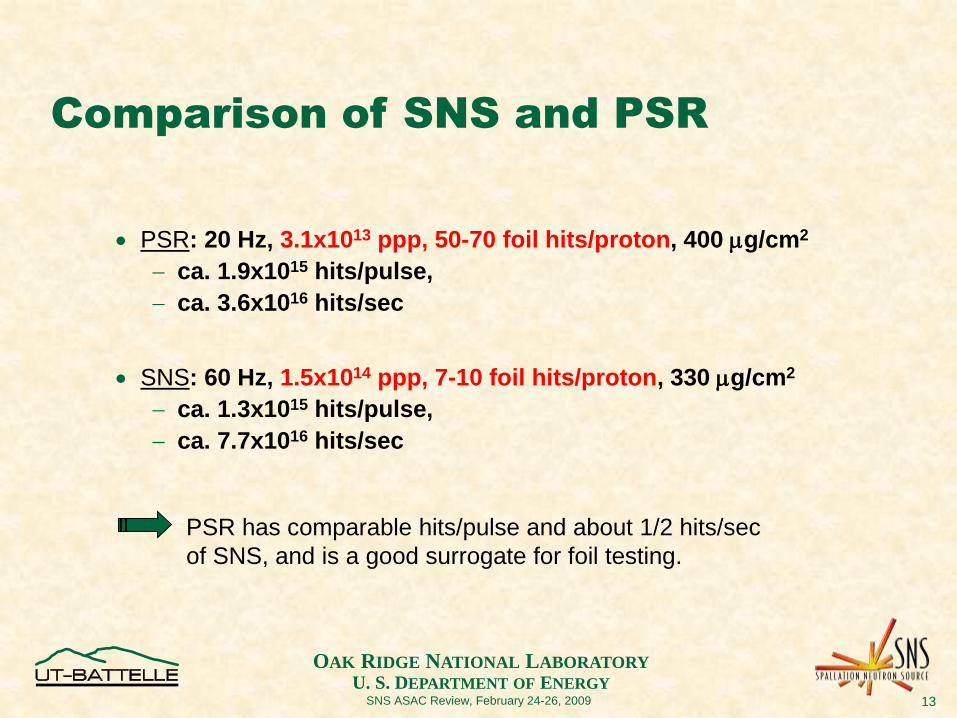
Comparison of SNS and PSR
PSR: 20 Hz, 3.1x10¹³ ppp, 50-70 foil hits/proton, 400 g/cm2
ca. 1.9x10¹⁵ hits/pulse,
ca. 3.6x10¹⁶ hits/sec
SNS: 60 Hz, 1.5x10¹⁴ ppp, 7-10 foil hits/proton, 330 g/cm2
ca. 1.3x10¹⁵ hits/pulse,
ca. 7.7x10¹⁶ hits/sec
PSR has comparable hits/pulse and about 1/2 hits/sec
of SNS, and is a good surrogate for foil testing.

OAK RIDGE NATIONAL LABORATORY
U. S. DEPARTMENT OF ENERGY14SNS ASAC Review, February 24-26, 2009
PSR Foil Experience
Failed
WNR
Loss
6 loadings since May 05
15 foils delivered
Current assessment is that nano-diamond foils perform well in production
(without fiber support), but fail catastrophically at high current density.
OAK RIDGE NATIONAL LABORATORY
U. S. DEPARTMENT OF ENERGY15SNS ASAC Review, February 24-26, 2009
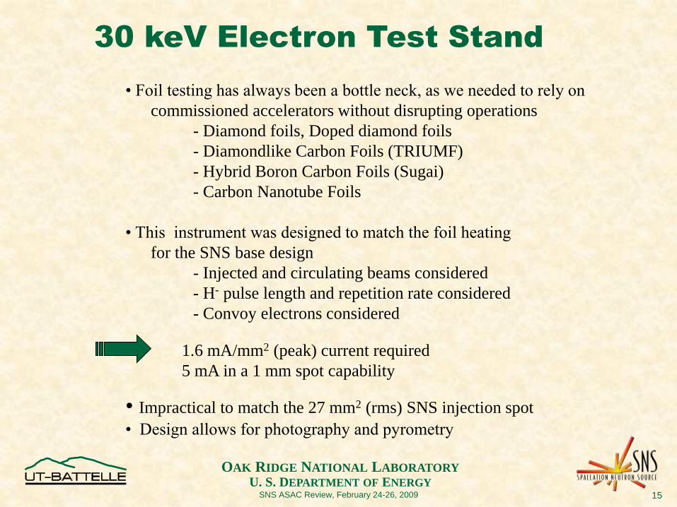
30 keV Electron Test Stand
• Foil testing has always been a bottle neck, as we needed to rely on
commissioned accelerators without disrupting operations
- Diamond foils, Doped diamond foils
- Diamondlike Carbon Foils (TRIUMF)
- Hybrid Boron Carbon Foils (Sugai)
- Carbon Nanotube Foils
• This instrument was designed to match the foil heating
for the SNS base design
- Injected and circulating beams considered
- H- pulse length and repetition rate considered
- Convoy electrons considered
1.6 mA/mm2 (peak) current required
5 mA in a 1 mm spot capability
• Impractical to match the 27 mm2 (rms) SNS injection spot
• Design allows for photography and pyrometry
OAK RIDGE NATIONAL LABORATORY
U. S. DEPARTMENT OF ENERGY16SNS ASAC Review, February 24-26, 2009
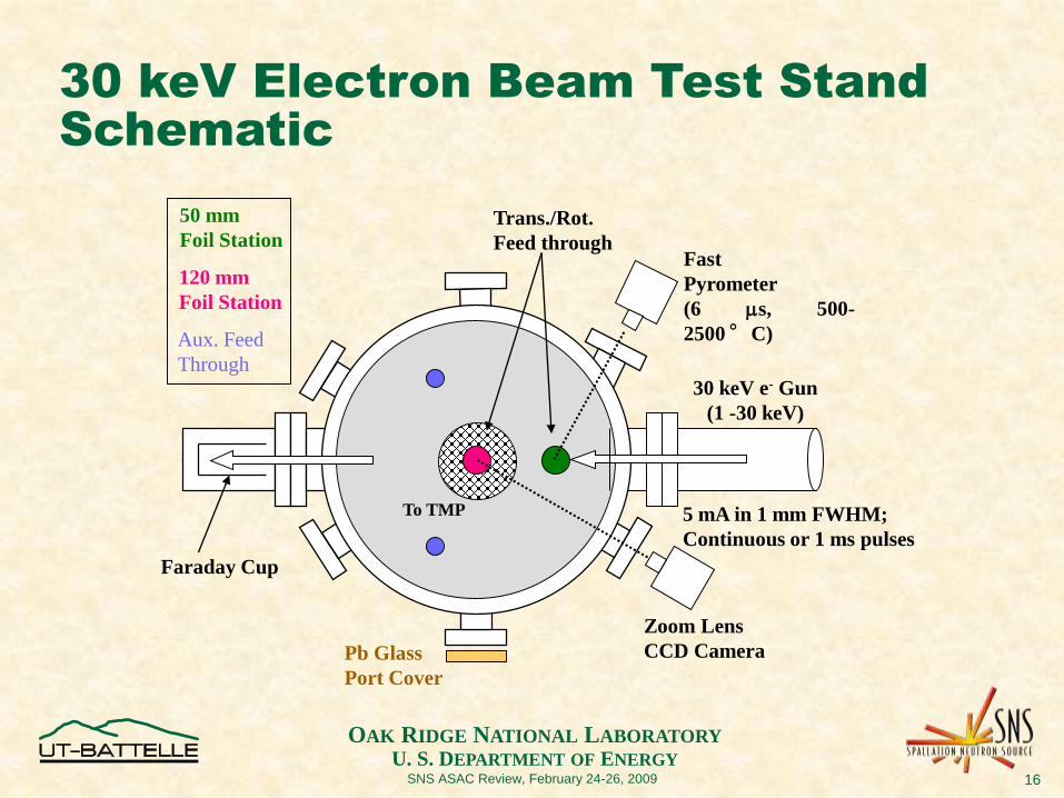
30 keV Electron Beam Test Stand
Schematic
To TMP
30 keV e- Gun
(1 -30 keV)
Faraday Cup
Fast
Pyrometer
(6 s, 500-
2500°C)
Zoom Lens
CCD CameraPb Glass
Port Cover
5 mA in 1 mm FWHM;
Continuous or 1 ms pulses
Trans./Rot.
Feed through
50 mm
Foil Station
120 mm
Foil Station
Aux. Feed
Through

OAK RIDGE NATIONAL LABORATORY
U. S. DEPARTMENT OF ENERGY17SNS ASAC Review, February 24-26, 2009
Electron Beam Foil Test Stand
Ready for Bakeout

OAK RIDGE NATIONAL LABORATORY
U. S. DEPARTMENT OF ENERGY18SNS ASAC Review, February 24-26, 2009
Electron Beam on Diamond Foil
• Snapshot camera without zoom

OAK RIDGE NATIONAL LABORATORY
U. S. DEPARTMENT OF ENERGY19SNS ASAC Review, February 24-26, 2009
Zoom CCD Camera for Foil Photography
<50 mm Back Port II.png>
<12 X Zoom @ window.png>
OAK RIDGE NATIONAL LABORATORY
U. S. DEPARTMENT OF ENERGY20SNS ASAC Review, February 24-26, 2009
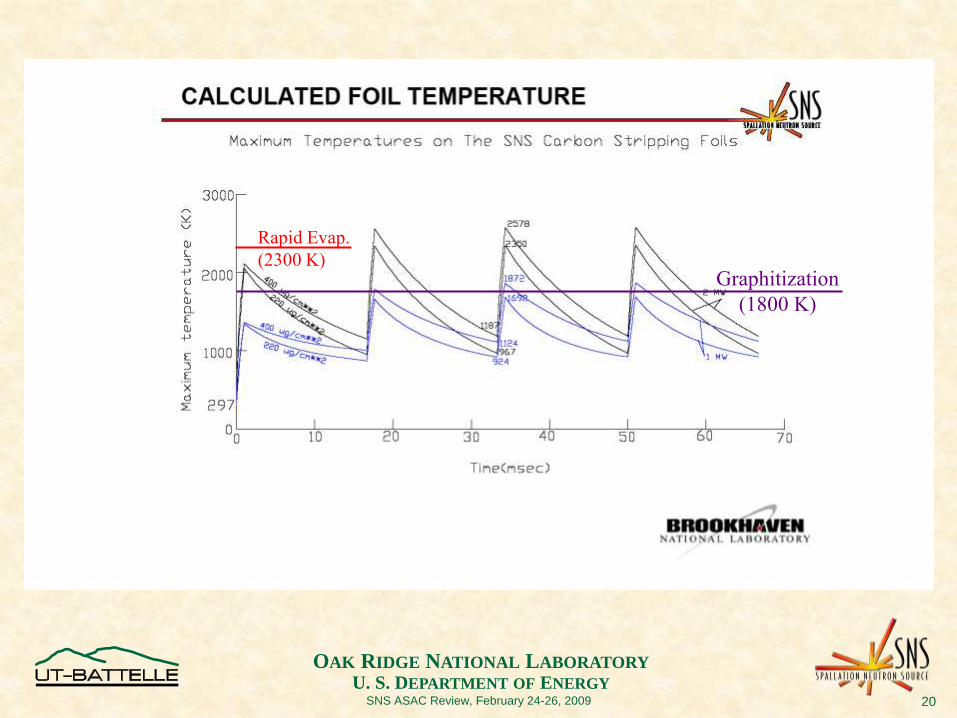
Graphitization
(1800 K)
Rapid Evap.
(2300 K)

OAK RIDGE NATIONAL LABORATORY
U. S. DEPARTMENT OF ENERGY21SNS ASAC Review, February 24-26, 2009
New Directions
• New corrugation patterns.
Growth of Hybrid Boron Carbon (HBC) foils.

OAK RIDGE NATIONAL LABORATORY
U. S. DEPARTMENT OF ENERGY22SNS ASAC Review, February 24-26, 2009
Initial Foil Corrugation Pattern
Variables:
• Pitch (25, 50, 100 L/in)
• Radius (1, 2, 3 mm)
• Coverage (40, 60%)

OAK RIDGE NATIONAL LABORATORY
U. S. DEPARTMENT OF ENERGY23SNS ASAC Review, February 24-26, 2009
New
Lithography
Mask
Patterns
= Flat @ RT
= Not bad
#601

OAK RIDGE NATIONAL LABORATORY
U. S. DEPARTMENT OF ENERGY24SNS ASAC Review, February 24-26, 2009
Hybrid Boron Carbon (HBC) Foils
• Isao Sugai has reported HBC foils with
excellent life times for proton beams.
- 20-25% Boron
- 256 hr lifetimes vs 62 hr for nano-diamond
• Limitations: Thickness < 400 g/cm2
Pinholes
Carbon fiber mounting
• We have begun to prepare similar foils using
our PA-CVD growth reactor.
Graphite Graphite/Boron
Substrate

OAK RIDGE NATIONAL LABORATORY
U. S. DEPARTMENT OF ENERGY25SNS ASAC Review, February 24-26, 2009
KEK Foil Comparison: HBC and Nano-diamond
(I. Sugai, ICFA5; Nashville, August 08)
Hybrid Boron Carbon (HBC)
SNS nanocrystalline diamond
• Single HBC foil (417 m/cm2)
with SiC fibers
• 650 keV dc H- beam (3.5 mm)
• 90 A; T = 1970 K
• 256 hr
• 30% thickness reduction
• SNS nanocrystalline foil #527 (433 g/cm2)
without fibers
• 130 A; T = 1950K
• 21 hr
• 6.5% thickness reduction
• “Inside curling”
OAK RIDGE NATIONAL LABORATORY
U. S. DEPARTMENT OF ENERGY26SNS ASAC Review, February 24-26, 2009
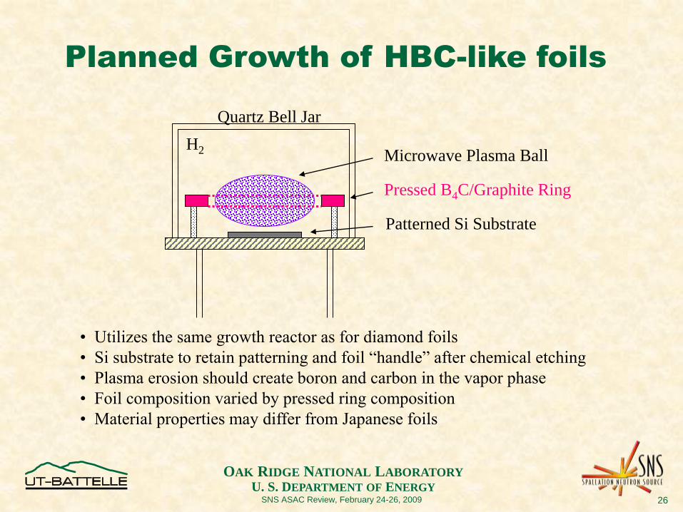
Pressed B4C/Graphite Ring
Patterned Si Substrate
Microwave Plasma Ball
Quartz Bell Jar
H2
Planned Growth of HBC-like foils
• Utilizes the same growth reactor as for diamond foils
• Si substrate to retain patterning and foil “handle” after chemical etching
• Plasma erosion should create boron and carbon in the vapor phase
• Foil composition varied by pressed ring composition
• Material properties may differ from Japanese foils

OAK RIDGE NATIONAL LABORATORY
U. S. DEPARTMENT OF ENERGY27SNS ASAC Review, February 24-26, 2009
SNS Foil Development Program
Summary
• Corrugated, nano-diamond stripper foils have performed well at
SNS and PSR.
• Improved techniques for growth and characterization
have been developed.
- Nano-seeding for nucleation
- Alpha ranging for thickness determination
• For an upgraded SNS, different materials may be needed.
• An e-beam test stand has been assembled to increase
throughput for foil lifetime testing for a variety of materials.
- Doped diamond, HBC, Carbon nanotubes
• Growth of another material has begun - HBC.

OAK RIDGE NATIONAL LABORATORY
U. S. DEPARTMENT OF ENERGY28SNS ASAC Review, February 24-26, 2009
Thank You !
OAK RIDGE NATIONAL LABORATORY
U. S. DEPARTMENT OF ENERGY29SNS ASAC Review, February 24-26, 2009
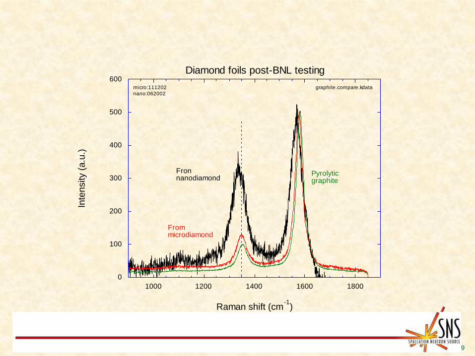
0
100
200
300
400
500
600
1000 1200 1400 1600 1800
graphite.compare.kdataIn
tensity (
a.u
.)
Raman shift (cm-1
)
Fronnanodiamond
Frommicrodiamond
Pyrolyticgraphite
Diamond foils post-BNL testing
micro:111202
nano:062002

OAK RIDGE NATIONAL LABORATORY
U. S. DEPARTMENT OF ENERGY30SNS ASAC Review, February 24-26, 2009