sns foil development program - neutron science at ornl · sns foil development program ... • no...
TRANSCRIPT

SNS Foil Development
Program
Robert Shaw
Chemical Sciences Division
Co-authors: Mike Plum, Chris Luck, SNS
L. Wilson, ORNL, and C.S. Feigerle (UT/K)
February 2-4, 2010

2 Managed by UT-Battellefor the U.S. Department of Energy SNSAAC Review, February 2-4, 2010
Outline
• Corrugated, nanocrystalline diamond SNS foils
• 30 keV electron beam test stand
• Diamond vs carbon stripping efficiency
• Foil charging - How can we make our diamond foils more electrically conducting?
• Hybrid Boron Carbon (HBC) foils
• Summary / Future directions

3 Managed by UT-Battellefor the U.S. Department of Energy SNSAAC Review, February 2-4, 2010
Nanodiamond foils at SNS
Requirements:
• Withstand peak temperatures up to 2500 K ???
• Stripping efficiency of 97% (of intercepted beam)
• Foil set of 10 foils must last 90 day cycle --> 200 hr each
• 20 mm x 12 mm freestanding foil, single edge support
• Uniform thickness of 280 g/cm2 (~0.8 m for diamond)
• Nanodiamond foils were in use on the 1st day neutrons were created and when the
1 MW threshold was crossed.
• 130 foils delivered; 54 foils mounted in 10 loadings.
• No foil failures until the May 2009 problems (details in M. Plum presentation)
• Recent Good News:
During the last cycle, a single foil served for the entire campaign (4820 Coulomb*).
(* 1 month at 1.4 MW ~ 3500 C)
4 Managed by UT-Battellefor the U.S. Department of Energy SNSAAC Review, February 2-4, 2010
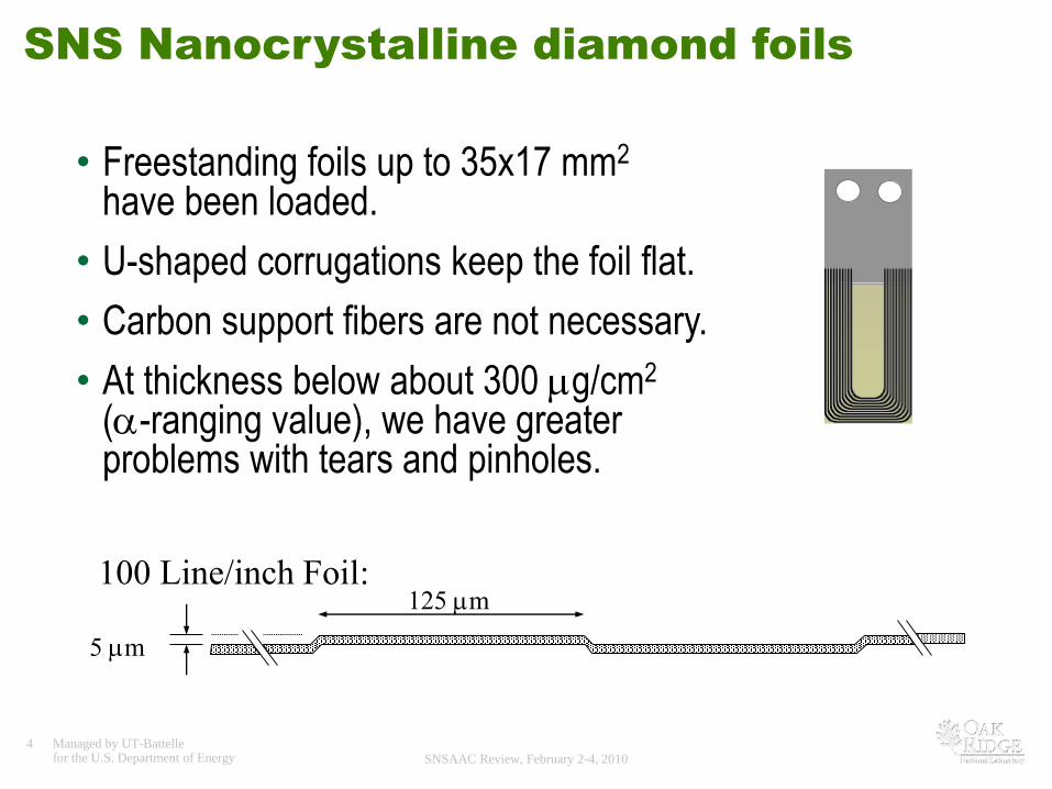
SNS Nanocrystalline diamond foils
• Freestanding foils up to 35x17 mm2
have been loaded.
• U-shaped corrugations keep the foil flat.
• Carbon support fibers are not necessary.
• At thickness below about 300 g/cm2
(-ranging value), we have greater problems with tears and pinholes.
100 Line/inch Foil:125 m
5 m

5 Managed by UT-Battellefor the U.S. Department of Energy SNSAAC Review, February 2-4, 2010
Summer / Fall 2009
Production - -
Foil Statistics
• Foil thickness deviation is ±5%
• 70% of foils scored ≥ “3”
• Lack of foils <300 g/cm2 due to high production failure rate

6 Managed by UT-Battellefor the U.S. Department of Energy SNSAAC Review, February 2-4, 2010
30 keV Electron Beam Test Stand
Schematic
• Foil testing has always been a bottle neck.
• Test stand designed to match the SNS foil heating.
1.6 mA/mm2 (peak) current required
5 mA in a 1 mm spot capability
To TMP
30 keV e- Gun
(1 -30 keV)
Faraday Cup
Fast
Pyrometer
(6 s, 500-
2500°C)
Zoom Lens
CCD CameraPb Glass
Port Cover
5 mA in 1 mm FWHM;
Continuous or 1 ms pulses
Trans./Rot.
Feed through 50 mm
Foil Station
120 mm
Foil Station
Aux. Feed
Through

7 Managed by UT-Battellefor the U.S. Department of Energy SNSAAC Review, February 2-4, 2010
Electron beam foil test stand

8 Managed by UT-Battellefor the U.S. Department of Energy SNSAAC Review, February 2-4, 2010
Electron beam test stand results
Foil temperature excursions for ~ 0.8X the simulated SNS power loading
0.24 mA current; 385 g/cm2
1070 °C
580 °CElectron beam profile:
Comparing the damage spots
to the foil corrugation pattern -
Diameter < 0.5 mm

9 Managed by UT-Battellefor the U.S. Department of Energy SNSAAC Review, February 2-4, 2010
Graphitization
(1800 K)
Rapid Evap.
(2300 K)
Foil temperatures measured using the test stand
for different materials and power loadings will give
us an indication how foils will fare at 1.4 and 3 MW.

10 Managed by UT-Battellefor the U.S. Department of Energy SNSAAC Review, February 2-4, 2010
Carlos Reinhold stripping efficiency
calculations
Dominant processes for H- stripping in carbon:
- inelastic e-e collisions (one e of H-; one e in foil)
- elastic collisions (one e of H-; screened C nucleus)
F(H-) ~ e(-x/L) where x= foil thickness; Lt = total MFP
1/Lt ~ 1/Li + 1/Le
Elastic MFP ~ 1/Density
Inelastic MFP ~ Same for diamond and carbon
(even though diamond is more dense;
harder to excite the e’s in diamond)
Total MFP: Carbon > Diamond
Problem:
20% thicker SNS foils will create substantially greater foil scattering.
To get the same stripping efficiency,
must use 20% thicker diamond foil (g/cm2)

11 Managed by UT-Battellefor the U.S. Department of Energy SNSAAC Review, February 2-4, 2010
Stripping efficiency of diamond vs. graphite
12 Managed by UT-Battellefor the U.S. Department of Energy SNSAAC Review, February 2-4, 2010
SNS foil charging
• Secondary electron emission from both foil faces due to proton passage.
• Thermionic emission, if foil is hot enough
• If the foil is an insulator, it will charge up and distort, break apart, or arc
• Applied bias on the SNS clearing electrode deflects foils, even before
they are exposed to the proton beam
• The PSR experience with SNS nanodiamond foils is that the foil current
dissipates in < 1 ms between the pulses
Is SNS foil flutter caused by foil charging ?
• Diamond resistivity can be altered by doping:
- We are beginning to dope our foils with boron using B metal
- Collaborating with Fraunhofer/MSU for boron doped nanodiamond
- Collaborating with Argonne for nitrogen doped nanodiamond

13 Managed by UT-Battellefor the U.S. Department of Energy SNSAAC Review, February 2-4, 2010
Doped Diamond
4000 -cm
• B2H6 or BF3 in CVD gas mixture
yields B doped diamond
• Hazardous, toxic gases
• At the foil operating T,
will boron stay put?
• As grown CVD diamond (xstal): = 1x10⁷ -cm
• Annealed CVD diamond: = 1x10¹³ -cm
• For 1 x 1 cm x 1 m 1017
• decreases slightly with temperature

14 Managed by UT-Battellefor the U.S. Department of Energy SNSAAC Review, February 2-4, 2010
Measuring diamond foil resistivity
Measured resistance: (3 samples)
• ~ 200 k17 x 15 mm x 1 m)
• Corresponds to ~ 25 -cm
So why are the foils so sensitive to static charge ?
• Nanocrystalline material has increased
grain boundary content that contains
defective “graphitic” material.
• Resistivity = ????
• For reference: the Si we use is = 10 -cm

15 Managed by UT-Battellefor the U.S. Department of Energy SNSAAC Review, February 2-4, 2010
Low resistance nanodiamond foil
that can charge up in the SNS beam
16 Managed by UT-Battellefor the U.S. Department of Energy SNSAAC Review, February 2-4, 2010
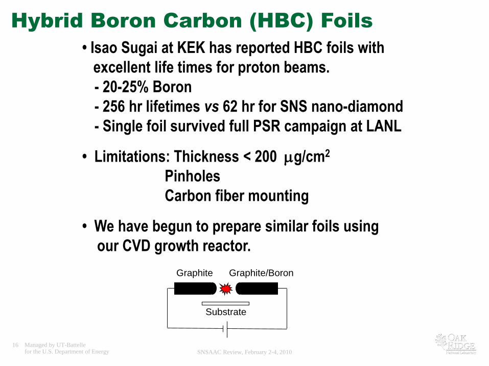
Hybrid Boron Carbon (HBC) Foils
• Isao Sugai at KEK has reported HBC foils with
excellent life times for proton beams.
- 20-25% Boron
- 256 hr lifetimes vs 62 hr for SNS nano-diamond
- Single foil survived full PSR campaign at LANL
• Limitations: Thickness < 200 g/cm2
Pinholes
Carbon fiber mounting
• We have begun to prepare similar foils using
our CVD growth reactor.
Graphite Graphite/Boron
Substrate

17 Managed by UT-Battellefor the U.S. Department of Energy SNSAAC Review, February 2-4, 2010
Concept for Growth of HBC-like foils

18 Managed by UT-Battellefor the U.S. Department of Energy SNSAAC Review, February 2-4, 2010
SNS Foil Development Program
Summary
• Corrugated, nanodiamond stripper foils have performed well at SNS.
• Diamond vs carbon stripping efficiency has been compared.
• Nanodiamond foil resistivites have been measured.
• Preparation of more conductive foils is underway.
- Boron doping
- Thin metallic coating ?
Future directions
• New corrugation patterns for increased foil flatness.
• Different materials may be necessary for the SNS upgrade to 3 MW.
- Growth of other materials emphasized (doped diamond, HBC, B4C)
- The e-beam test stand will be used for foil lifetime and Tmax testing for
several materials - doped diamond, DLC, HBC, carbon nanotube foils

19 Managed by UT-Battellefor the U.S. Department of Energy SNSAAC Review, February 2-4, 2010
Thank You !

20 Managed by UT-Battellefor the U.S. Department of Energy SNSAAC Review, February 2-4, 2010
Back-up Slides

21 Managed by UT-Battellefor the U.S. Department of Energy SNSAAC Review, February 2-4, 2010
SNS Foil Requirements
H- from linac
H+ from ring H+ to ring
e- to collector
• Withstand peak temperatures up to 2500 K ???
• Stripping efficiency of 97% (of intercepted beam)
• Foil set of 10 foils must last 90 day cycle --> 200 hr each
• 20 mm x 12 mm (35 x 17) freestanding foil, single edge support
• Uniform thickness of 280 g/cm2 (~0.8 m for diamond)

22 Managed by UT-Battellefor the U.S. Department of Energy SNSAAC Review, February 2-4, 2010
“Normal” foil failure mode
<601 looking upstream.jpg>
Photograph of a nanocrystalline SNS foil (#601; 463 ug/cm2 avg) after
experiencing 300 C of injected charge. The lower left corner is curled away from the
camera from interaction with the injected and circulating ion beam.

23 Managed by UT-Battellefor the U.S. Department of Energy SNSAAC Review, February 2-4, 2010
Carlos
Reinhold
Results