slvs803d –november 2008–revised january … –november 2008–revised january 2015 tps2290x...
TRANSCRIPT

ON
OFFC = 1 FIN
µ
GNDGND
GND
VOUT
LOADV
INV
BATT
RL
CLC
L
SMPS
TPS22901/02/02B(see Note A)
Product
Folder
Sample &Buy
Technical
Documents
Tools &
Software
Support &Community
TPS22901, TPS22902, TPS22902BSLVS803D –NOVEMBER 2008–REVISED JANUARY 2015
TPS2290x 3.6-V, 500-mA, 78-mΩ ON-Resistance Load Switch With Controlled Turnon1 Features 2 Applications1• Integrated P-Channel Load Switch • Personal Digital Assistants (PDAs)• Low Input Voltage: 1 V to 3.6 V • Cellular Phones• ON-Resistance (Typical Values) • GPS Devices
• MP3 Players– rON = 78 mΩ at VIN = 3.6 V• Digital Cameras– rON = 93 mΩ at VIN = 2.5 V• Peripheral Ports– rON = 109 mΩ at VIN = 1.8 V• Portable Instrumentation– rON = 146 mΩ at VIN = 1.2 V• RF Modules• 500 mA Maximum Continuous Switch Current
• Quiescent Current: 82 nA at 1.8 V3 Description• Shutdown Current: 44 nA at 1.8 VThe TPS22901, TPS22902, and TPS22902B are• Low Control Input Thresholds Enable Use of small, low ON-resistance (rON) load switches with a
1.2-V, 1.8-V, 2.5-V, and 3.3-V Logic controlled turnon. These devices contain a P-channel• Controlled Slew Rate to Avoid Inrush Currents MOSFET that operates over an input voltage range of
1.0 V to 3.6 V. The switch is controlled by an on/off– tr = 40 μs at VIN = 1.8 V (TPS22901/2)input (ON), which can interface directly with low-– tr = 220 μs at VIN = 1.8 V (TPS22902B) voltage control signals. In the TPS22902 and
• Quick Output Discharge (TPS22902/2B) TPS22902B, an 88-Ω on-chip load resistor is addedfor output quick discharge when the switch is turned• ESD Performance Tested Per JESD 22off.– 2000-V Human Body ModelThe TPS22901, TPS22902, and TPS22902B are(A114-B, Class II)available in a space-saving 4-pin DSBGA (YFP) with– 1000-V Charged-Device Model (C101)0.4-mm pitch. These devices are characterized for
• Four-Pin Wafer-Chip-Scale DSBGA Package operation over the free-air temperature range of– 0.8-mm × 0.8-mm, 0.4-mm Pitch, –40°C to 85°C.
0.5-mm Height (YFP)Device Information(1)
PART NUMBER PACKAGE BODY SIZE (NOM)TPS22901TPS22902 DSBGA (4) 0.80 mm × 0.80 mmTPS22902B
(1) For all available packages, see the orderable addendum atthe end of the data sheet.
4 Typical Application Schematic
A. Switched-mode power supply
1
An IMPORTANT NOTICE at the end of this data sheet addresses availability, warranty, changes, use in safety-critical applications,intellectual property matters and other important disclaimers. PRODUCTION DATA.
TPS22901, TPS22902, TPS22902BSLVS803D –NOVEMBER 2008–REVISED JANUARY 2015 www.ti.com
Table of Contents1 Features .................................................................. 1 9 Parameter Measurement Information ................ 192 Applications ........................................................... 1 10 Detailed Description ........................................... 20
10.1 Overview ............................................................... 203 Description ............................................................. 110.2 Functional Block Diagram ..................................... 204 Typical Application Schematic ............................. 110.3 Feature Description............................................... 205 Revision History..................................................... 210.4 Device Functional Modes...................................... 206 Device Comparison Table ..................................... 3
11 Application and Implementation........................ 217 Pin Configuration and Functions ......................... 311.1 Application Information.......................................... 218 Specifications......................................................... 411.2 Typical Application ................................................ 218.1 Absolute Maximum Ratings ..................................... 4
12 Power Supply Recommendations ..................... 248.2 ESD Ratings.............................................................. 413 Layout................................................................... 248.3 Recommended Operating Conditions....................... 4
13.1 Layout Guidelines ................................................. 248.4 Thermal Information .................................................. 413.2 Layout Example .................................................... 248.5 Electrical Characteristics........................................... 5
14 Device and Documentation Support ................. 258.6 Switching Characteristics (VIN = 1.1 V)..................... 614.1 Related Links ........................................................ 258.7 Switching Characteristics (VIN = 1.2 V)..................... 614.2 Trademarks ........................................................... 258.8 Switching Characteristics (VIN = 1.8 V)..................... 714.3 Electrostatic Discharge Caution............................ 258.9 Switching Characteristics (VIN = 2.5 V)..................... 714.4 Glossary ................................................................ 258.10 Switching Characteristics (VIN = 3.0 V)................... 8
15 Mechanical, Packaging, and Orderable8.11 Switching Characteristics (VIN = 3.6 V)................... 8Information ........................................................... 258.12 Typical DC Characteristics...................................... 9
5 Revision HistoryNOTE: Page numbers for previous revisions may differ from page numbers in the current version.
Changes from Revision C (December 2012) to Revision D Page
• Added ESD Rating table, Feature Description section, Device Functional Modes, Application and Implementationsection, Power Supply Recommendations section, Layout section, Device and Documentation Support section, andMechanical, Packaging, and Orderable Information section. ................................................................................................. 1
• Deleted the ORDERING INFORMATION table...................................................................................................................... 3
Changes from Revision B (March 2009) to Revision C Page
• Changed the ORDERING INFORMATION table.................................................................................................................... 3
2 Submit Documentation Feedback Copyright © 2008–2015, Texas Instruments Incorporated
Product Folder Links: TPS22901 TPS22902 TPS22902B
Laser Marking View Bump View
B
2 1
A
B
1 2
A
TPS22901, TPS22902, TPS22902Bwww.ti.com SLVS803D –NOVEMBER 2008–REVISED JANUARY 2015
6 Device Comparison Table
RON at 1.8 V RISE TIME QUICK OUTPUT MAX OUTPUT ENABLE(TYP) (TYP at 1.8 V) DISCHARGE (1) CURRENTTPS22901 No
40 μsTPS22902 109 mΩ Yes 500 mA Active highTPS22902B 220 μs Yes
(1) This feature discharges the output of the switch to ground through an 88 Ω resistor, preventing theoutput from floating.
7 Pin Configuration and Functions
YFP Package4-Pin DSBGA
Pin AssignmentsB ON GNDA VIN VOUT
2 1
Pin FunctionsPIN
I/O DESCRIPTIONNO. NAMEA1 VOUT O Switch outputA2 VIN I Switch input, bypass this input with a ceramic capacitor to groundB1 GND - GroundB2 ON I Switch control input, active high
Copyright © 2008–2015, Texas Instruments Incorporated Submit Documentation Feedback 3
Product Folder Links: TPS22901 TPS22902 TPS22902B

TPS22901, TPS22902, TPS22902BSLVS803D –NOVEMBER 2008–REVISED JANUARY 2015 www.ti.com
8 Specifications
8.1 Absolute Maximum Ratingsover operating free-air temperature range (unless otherwise noted) (1)
MIN MAX UNITVIN Input voltage –0.3 4 VVOUT Output voltage VIN + 0.3 VVON Input voltage –0.3 4 VP Power dissipation at TA = 25°C 0.48 WIMAX Maximum continuous switch current 500 mATA Operating free-air temperature –40 85 °CTlead Maximum lead temperature (10-s soldering time) 300 °CTstg Storage temperature –65 150 °C
(1) Stresses beyond those listed under Absolute Maximum Ratings may cause permanent damage to the device. These are stress ratingsonly, which do not imply functional operation of the device at these or any other conditions beyond those indicated under RecommendedOperating Conditions. Exposure to absolute-maximum-rated conditions for extended periods may affect device reliability.
8.2 ESD RatingsVALUE UNIT
Human body model (HBM), per ANSI/ESDA/JEDEC JS-001 (1) ±2000V(ESD) Electrostatic discharge VCharged-device model (CDM), per JEDEC specification JESD22- ±1000
C101 (2)
(1) JEDEC document JEP155 states that 500-V HBM allows safe manufacturing with a standard ESD control process.(2) JEDEC document JEP157 states that 250-V CDM allows safe manufacturing with a standard ESD control process.
8.3 Recommended Operating ConditionsMIN MAX UNIT
VIN Input voltage 1 3.6 VVOUT Output voltage VIN VVIH High-level input voltage, ON 0.85 3.6 VVIL Low-level input voltage, ON 0.4 VCIN Input capacitor See (1) μF
(1) See Input Capacitor (Optional).
8.4 Thermal InformationTPS2290X
THERMAL METRIC (1) YFP (DSBGA) UNIT4 PINS
RθJA Junction-to-ambient thermal resistance 192.1RθJC(top) Junction-to-case (top) thermal resistance 2.3RθJB Junction-to-board thermal resistance 35.8 °C/WψJT Junction-to-top characterization parameter 11.8ψJB Junction-to-board characterization parameter 35.6
(1) For more information about traditional and new thermal metrics, see the IC Package Thermal Metrics application report, SPRA953.
4 Submit Documentation Feedback Copyright © 2008–2015, Texas Instruments Incorporated
Product Folder Links: TPS22901 TPS22902 TPS22902B
TPS22901, TPS22902, TPS22902Bwww.ti.com SLVS803D –NOVEMBER 2008–REVISED JANUARY 2015
8.5 Electrical CharacteristicsVIN = 1.0 V to 3.6 V, TA = –40°C to 85°C (unless otherwise noted). Typical values are for TA = 25°C
PARAMETER TEST CONDITIONS TA MIN TYP MAX UNITVIN = 1.1 V Full 37 120
IQ Quiescent current IOUT = 0, VIN = VON VIN = 1.8 V Full 82 235 nAVIN = 3.6 V Full 204 880VIN = 1.1 V Full 22 210
IIN(OFF) OFF-state supply current VON = GND, VOUT = Open VIN = 1.8 V Full 44 260 nAVIN = 3.6 V Full 137 700VIN = 1.1 V Full 22 140
IIN(LEAKAGE) OFF-state switch current VON = GND, VOUT = 0 V VIN = 1.8 V Full 45 230 nAVIN = 3.6 V Full 137 610
25°C 78 95VIN = 3.6 V
Full 9525°C 93 110
VIN = 2.5 VFull 110
25°C 109 130rON ON-state resistance IOUT = - 200 mA VIN = 1.8 V mΩ
Full 13025°C 146 200
VIN = 1.2 VFull 200
25°C 174 330VIN = 1.1 V
Full 330VIN = 3.3 V, VON = 0, IOUT = 30 mArPD Output pulldown resistance 25°C 88 120 Ω(TPS22902/TPS22902B only)
ION ON input leakage current VON = 1.1 V to 3.6 V or GND Full 25 nA
Copyright © 2008–2015, Texas Instruments Incorporated Submit Documentation Feedback 5
Product Folder Links: TPS22901 TPS22902 TPS22902B
TPS22901, TPS22902, TPS22902BSLVS803D –NOVEMBER 2008–REVISED JANUARY 2015 www.ti.com
8.6 Switching Characteristics (VIN = 1.1 V)VIN = 1.1 V, TA = 25°C (unless otherwise noted)
TPS22901 TPS22902 (1) TPS22902B (1)PARAMETER TEST CONDITIONS UNIT
MIN TYP MAX MIN TYP MAX MIN TYP MAXCL = 0.1 μF 108 108 531
tON Turn-ON time RL = 500 Ω CL = 1 μF 131 131 596 μsCL = 3.3 μF 153 153 659CL = 0.1 μF 39 11 11
tOFF Turn-OFF time RL = 500 Ω CL = 1 μF 317 69 67 μsCL = 3.3 μF 1105 238 225CL = 0.1 μF 70 70 365
tr VOUT rise time RL = 500 Ω CL = 1 μF 78 78 367 μsCL = 3.3 μF 92 92 395CL = 0.1 μF 107 18 21
tf VOUT fall time RL = 500 Ω CL = 1 μF 966 175 189 μsCL = 3.3 μF 3532 632 565
(1) Quick Output Discharge
8.7 Switching Characteristics (VIN = 1.2 V)VIN = 1.2 V, TA = 25°C (unless otherwise noted)
TPS22901 TPS22902 (1) TPS22902B (1)PARAMETER TEST CONDITIONS UNIT
MIN TYP MAX MIN TYP MAX MIN TYP MAXCL = 0.1 μF 96 96 471
tON Turn-ON time RL = 500 Ω CL = 1 μF 116 116 527 μsCL = 3.3 μF 135 135 587CL = 0.1 μF 39 10 10
tOFF Turn-OFF time RL = 500 Ω CL = 1 μF 317 62 61 μsCL = 3.3 μF 1110 210 199CL = 0.1 μF 62 62 324
tr VOUT rise time RL = 500 Ω CL = 1 μF 69 69 325 μsCL = 3.3 μF 81 81 350CL = 0.1 μF 109 17 20
tf VOUT fall time RL = 500 Ω CL = 1 μF 995 163 175 μsCL = 3.3 μF 3650 587 523
(1) Quick Output Discharge
6 Submit Documentation Feedback Copyright © 2008–2015, Texas Instruments Incorporated
Product Folder Links: TPS22901 TPS22902 TPS22902B

TPS22901, TPS22902, TPS22902Bwww.ti.com SLVS803D –NOVEMBER 2008–REVISED JANUARY 2015
8.8 Switching Characteristics (VIN = 1.8 V)VIN = 1.8 V, TA = 25°C (unless otherwise noted)
TPS22901 TPS22902 (1) TPS22902B (1)PARAMETER TEST CONDITIONS UNIT
MIN TYP MAX MIN TYP MAX MIN TYP MAXCL = 0.1 μF 61 61 302
tON Turn-ON time RL = 500 Ω CL = 1 μF 72 72 335 μsCL = 3.3 μF 83 83 367CL = 0.1 μF 38 8 8
tOFF Turn-OFF time RL = 500 Ω CL = 1 μF 317 49 49 μsCL = 3.3 μF 1135 169 167CL = 0.1 μF 40 40 220
tr VOUT rise time RL = 500 Ω CL = 1 μF 45 45 220 μsCL = 3.3 μF 53 53 235CL = 0.1 μF 111 15 15
tf VOUT fall time RL = 500 Ω CL = 1 μF 1020 140 159 μsCL = 3.3 μF 3700 517 481
(1) Quick Output Discharge
8.9 Switching Characteristics (VIN = 2.5 V)VIN = 2.5 V, TA = 25°C (unless otherwise noted)
TPS22901 TPS22902 (1) TPS22902B (1)PARAMETER TEST CONDITIONS UNIT
MIN TYP MAX MIN TYP MAX MIN TYP MAXCL = 0.1 μF 45 45 223
tON Turn-ON time RL = 500 Ω CL = 1 μF 53 53 246 μsCL = 3.3 μF 61 61 268CL = 0.1 μF 38 7 7
tOFF Turn-OFF time RL = 500 Ω CL = 1 μF 314 46 47 μsCL = 3.3 μF 1140 161 158CL = 0.1 μF 32 32 175
tr VOUT rise time RL = 500 Ω CL = 1 μF 35 35 175 μsCL = 3.3 μF 41 41 187CL = 0.1 μF 113 14 18
tf VOUT fall time RL = 500 Ω CL = 1 μF 1040 139 185 μsCL = 3.3 μF 3795 516 471
(1) Quick Output Discharge
Copyright © 2008–2015, Texas Instruments Incorporated Submit Documentation Feedback 7
Product Folder Links: TPS22901 TPS22902 TPS22902B

TPS22901, TPS22902, TPS22902BSLVS803D –NOVEMBER 2008–REVISED JANUARY 2015 www.ti.com
8.10 Switching Characteristics (VIN = 3.0 V)VIN = 3.0 V, TA = 25°C (unless otherwise noted)
TPS22901 TPS22902 (1) TPS22902B (1)PARAMETER TEST CONDITIONS UNIT
MIN TYP MAX MIN TYP MAX MIN TYP MAXCL = 0.1 μF 38 38 191
tON Turn-ON time RL = 500 Ω CL = 1 μF 45 45 211 μsCL = 3.3 μF 53 53 231CL = 0.1 μF 38 7 7
tOFF Turn-OFF time RL = 500 Ω CL = 1 μF 320 46 46 μsCL = 3.3 μF 1145 53 156CL = 0.1 μF 28 28 159
tr VOUT rise time RL = 500 Ω CL = 1 μF 31 31 160 μsCL = 3.3 μF 37 37 170CL = 0.1 μF 114 14 17
tf VOUT fall time RL = 500 Ω CL = 1 μF 1045 139 160 μsCL = 3.3 μF 3815 509 473
(1) Quick Output Discharge
8.11 Switching Characteristics (VIN = 3.6 V)VIN = 3.6 V, TA = 25°C (unless otherwise noted)
TPS22901 TPS22902 (1) TPS22902B (1)PARAMETER TEST CONDITIONS UNIT
MIN TYP MAX MIN TYP MAX MIN TYP MAXCL = 0.1 μF 33 33 166
tON Turn-ON time RL = 500 Ω CL = 1 μF 39 39 183 μsCL = 3.3 μF 46 46 201CL = 0.1 μF 38 7 7
tOFF Turn-OFF time RL = 500 Ω CL = 1 μF 322 46 45 μsCL = 3.3 μF 1145 156 155CL = 0.1 μF 25 25 146
tr VOUT rise time RL = 500 Ω CL = 1 μF 28 28 146 μsCL = 3.3 μF 34 34 156CL = 0.1 μF 116 14 17
tf VOUT fall time RL = 500 Ω CL = 1 μF 1060 139 161 μsCL = 3.3 μF 3840 512 475
(1) Quick Output Discharge
8 Submit Documentation Feedback Copyright © 2008–2015, Texas Instruments Incorporated
Product Folder Links: TPS22901 TPS22902 TPS22902B
Input Voltage, V (V)IN
0
20
40
60
80
100
120
0.5 1.0 1.5 2.0 2.5 3.0 3.5 4.0
IC
urr
ent (n
A)
IN(O
FF
)
–40 25 85
Temperature(°C)
0
50
100
150
200
250
Quie
scent C
urr
ent, I
(nA
)IN
Input Voltage, V (V)IN
Quie
scent C
urr
ent, I
(nA
)IN
0
20
40
60
80
100
120
140
160
180
200
0.5 1.0 1.5 2.0 2.5 3.0 3.5 4.00.00 0.05 0.10 0.15 0.20 0.25 0.30 0.35 0.40 0.45 0.50
Load Current (A)
0
10
20
30
40
50
60
70
80
90
100
Voltage D
rop (
mV
) V = 1.0 Vdrop
V = 1.2 Vdrop
V = 1.8 Vdrop
V = 2.5 Vdrop
V = 3.3 Vdrop
ON
-Sta
te R
esis
tan
ce,
Ωr
(m)
ON
50
55
60
65
70
75
–40 25 85
Temperature(°C)Input Voltage, (V)VIN
ON
-Sta
te R
esis
tance,
()
r ON
Ω
0.0
0.1
0.2
0.3
0.4
0.5
0.6
0.7
0.8
0.9
1.0
0.7 0.8 0.9 1.0 1.1 1.2 1.3 1.4 1.5 1.6 1.7 1.8 1.9 2.0 2.1 2.2 2.3 2.4 2.5 2.6 2.7 2.8 2.9 3.0 3.1 3.2 3.3
TPS22901, TPS22902, TPS22902Bwww.ti.com SLVS803D –NOVEMBER 2008–REVISED JANUARY 2015
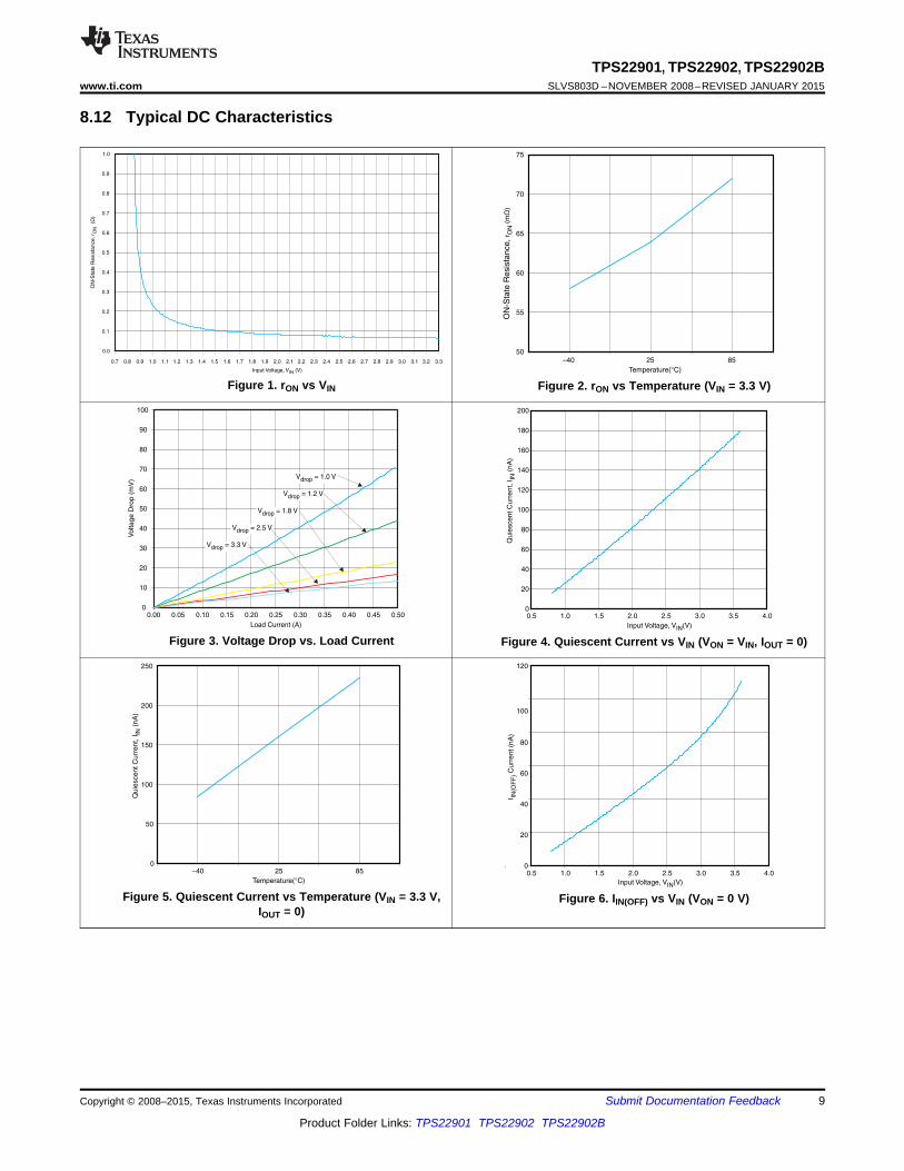
8.12 Typical DC Characteristics
Figure 1. rON vs VIN Figure 2. rON vs Temperature (VIN = 3.3 V)
Figure 3. Voltage Drop vs. Load Current Figure 4. Quiescent Current vs VIN (VON = VIN, IOUT = 0)
Figure 5. Quiescent Current vs Temperature (VIN = 3.3 V, Figure 6. IIN(OFF) vs VIN (VON = 0 V)IOUT = 0)
Copyright © 2008–2015, Texas Instruments Incorporated Submit Documentation Feedback 9
Product Folder Links: TPS22901 TPS22902 TPS22902B
I(L
eakage)
Curr
ent (n
A)
IN
0
25
50
75
100
125
150
175
200
225
250
–40 25 85
Temperature (°C)
–0.5
0.0
0.5
1.0
1.5
2.0
2.5
3.0
3.5
4.0
0.3 0.4 0.5 0.6 0.7 0.8
V(V
)O
UT
Input Voltage, V (V)ON
VIN = 3.6 V
VIN = 1.1 V
VIN = 1.2 V
VIN = 1.5 V
VIN = 1.8 V
VIN = 2.5 V
VIN = 3 V
VIN = 3.3 V
Input Voltage, (V)VIN
1.5 2.0 2.5 3.0 3.5 4.01.00.5
20
40
60
80
100
120
0
I(L
eakage)
Curr
ent (n
A)
IN
–40 25 85
Temperature(°C)
IC
urr
en
t (n
A)
IN(O
FF
)
25
50
75
100
125
150
175
200
225
250
0
TPS22901, TPS22902, TPS22902BSLVS803D –NOVEMBER 2008–REVISED JANUARY 2015 www.ti.com
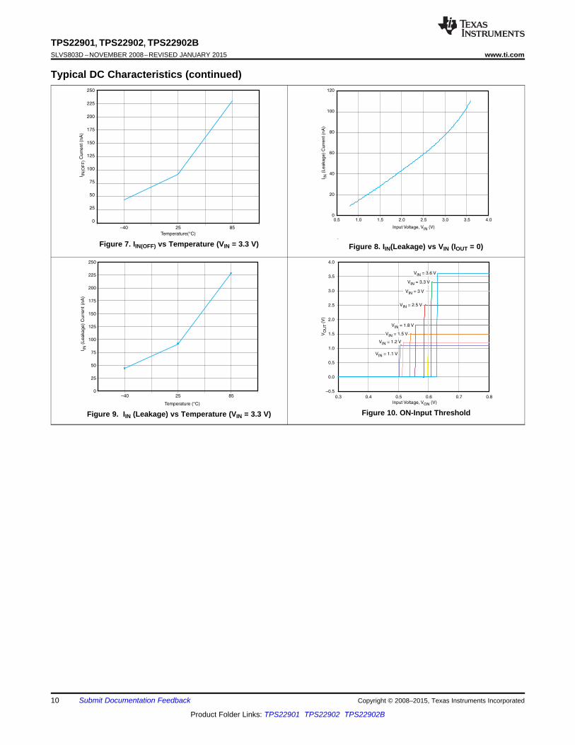
Typical DC Characteristics (continued)
Figure 7. IIN(OFF) vs Temperature (VIN = 3.3 V) Figure 8. IIN(Leakage) vs VIN (IOUT = 0)
Figure 10. ON-Input ThresholdFigure 9. IIN (Leakage) vs Temperature (VIN = 3.3 V)
10 Submit Documentation Feedback Copyright © 2008–2015, Texas Instruments Incorporated
Product Folder Links: TPS22901 TPS22902 TPS22902B
0
10
20
30
40
50
60
70
80
90
100
110
120
130
140
150
160
170
–50 –35 –20 –5 10 25 40 55 70 85 100
Temperature (°C)
V = 3.3 V
C = 0.1 F
R = 500
IN
L
L
µ
Ω
t/t
(s)
rise
fall
µ
trise
tfall
–50 –35 –20 –5 10 25 40 55 70 85 100
Temperature (°C)
t/t
(s)
ON
OF
Fµ
0
10
20
30
40
50
60
70
80
90
100
110
120
130
140
150
160
170
180
190
200
tOFF
V = 3.3 V
C = 0.1 F
R = 500
IN
L
L
µ
Ω
tON
10
12
14
16
18
20
22
24
26
28
30
–50 –40 –30 –20 –10 0 10 20 30 40 50 60 70 80 90 100
Temperature (°C)
V = 3.3 V
C = 0.1 F
R = 500
IN
L
L
µ
Ω
t/t
(s)
rise
fall
µ
trise
tfall
Temperature (°C)
t/t
(s)
ON
OF
Fµ
0
5
10
15
20
25
30
35
40
–50 –40 –30 –20 –10 0 10 20 30 40 50 60 70 80 90 100
tON
tOFF
V = 3.3 V
C = 0.1 F
R = 500
IN
L
L
µ
Ω
–50 –40 –30 –20 –10 0 10 20 30 40 50 60 70 80 90 100
Temperature (°C)
t/t
(s)
rise
fall
µ
10
20
30
40
50
60
70
80
90
100
110
120
130
trise
tfall
V = 3.3 V
C = 0.1 F
R = 500
IN
L
L
µ
Ω
Temperature (°C)
t/t
(s)
ON
OF
Fµ
–50 –40 –30 –20 –10 0 10 20 30 40 50 60 70 80 90 10028
30
32
34
36
38
40
42
V = 3.3 V
C = 0.1 F
R = 500
IN
L
L
µ
Ω
tON
tOFF
TPS22901, TPS22902, TPS22902Bwww.ti.com SLVS803D –NOVEMBER 2008–REVISED JANUARY 2015
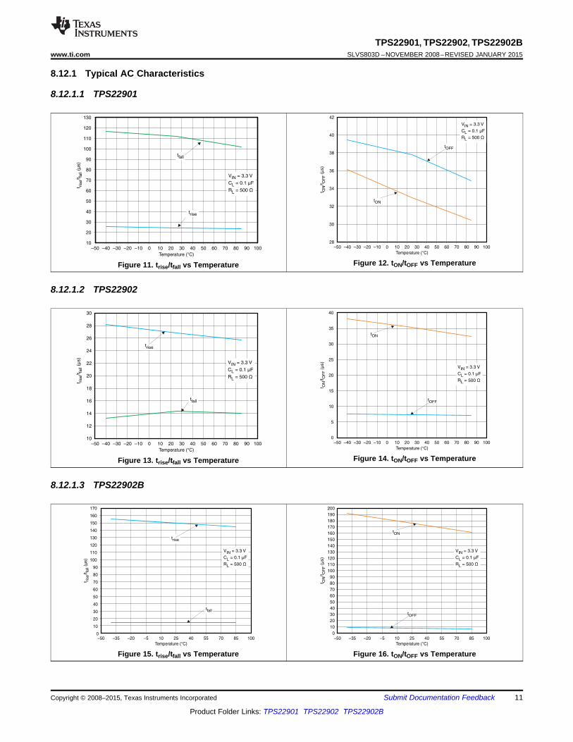
8.12.1 Typical AC Characteristics
8.12.1.1 TPS22901
Figure 12. tON/tOFF vs TemperatureFigure 11. trise/tfall vs Temperature
8.12.1.2 TPS22902
Figure 14. tON/tOFF vs TemperatureFigure 13. trise/tfall vs Temperature
8.12.1.3 TPS22902B
Figure 15. trise/tfall vs Temperature Figure 16. tON/tOFF vs Temperature
Copyright © 2008–2015, Texas Instruments Incorporated Submit Documentation Feedback 11
Product Folder Links: TPS22901 TPS22902 TPS22902B

Time ( s)µ
Contr
ol I
nput V
olta
ge (
V)
2.00
1.80
1.60
–0.40
–0.60
–0.20
0.00
0.20
0.40
0.60
0.80
1.00
1.20
1.40
–2.00
–1.80
–1.00
–1.40
–1.60
–0.80
–1.20
4.00
3.50
3.00
–0.50
0.00
0.50
1.00
1.50
2.00
2.50
–4.00
–3.50
–1.50
–2.50
–3.00
–1.00
–2.00
Outp
ut C
urr
ent (m
A)
C = 0.1 F
R = 500
V = 1.2 V
L
L
IN
µ
Ω
IOUT
VON
–50 0 50 100 150 200 250 300 350 450400
Time ( s)µ
Contr
ol I
nputV
olta
ge (
V)
2.00
1.80
1.60
–0.40
–0.60
–0.20
0.00
0.20
0.40
0.60
0.80
1.00
1.20
1.40
–2.00
–1.80
–1.00
–1.40
–1.60
–0.80
–1.20
199
180
160
–20
0.0
60
20
80
40
100
120
140
–200
–180
–80
–140
–160
–40
–60
–100
–120
Outp
ut C
urr
ent (m
A)
C = 0.1 F
R = 11
V = 1.2 V
L
L
IN
µ
Ω
IOUT
VON
–50 0 50 100 150 200 250 300 350 450400
Time ( s)µ
Contr
ol I
nput V
olta
ge (
V)
–50 0 50 100 150 200 250 300 350 450400
2.00
1.80
1.60
–0.40
–0.60
–0.20
0.00
0.20
0.40
0.60
0.80
1.00
1.20
1.40
–2.00
–1.80
–1.00
–1.40
–1.60
–0.80
–1.20
8.00
7.00
6.00
–1.00
0.000.0051.00
2.00
3.00
4.00
5.00
–8.00
–7.00
–3.00
–5.00
–6.00
–2.00
–4.00
Outp
ut C
urr
ent (m
A)
C = 3.3 F
R = 500
V = 3.3 V
L
L
IN
µ
Ω
IOUT
VON
Time (µs)
Contr
ol I
nputV
olta
ge (
V)
2.00
1.80
1.60
–0.40
–0.60
–0.20
0.00
0.20
0.40
0.60
0.80
1.00
1.20
1.40
–2.00
–1.80
–1.00
–1.40
–1.60
–0.80
–1.20
400
350
300
–50
0.0
50
100
150
200
250
–400
–350
–150
–250
–300
–100
–200
Outp
ut C
urr
ent (m
A)
C = 3.3 F
R = 11
V = 3.3 V
L
L
IN
µ
Ω
IOUT
VON
–50 0 50 100 150 200 250 300 350 450400
Time ( s)µ
Contr
ol I
nput V
olta
ge (
V)
–50 0 50 100 150 200 250 300 350 450400
2.00
1.80
1.60
–0.40
–0.60
–0.20
0.00
0.20
0.40
0.60
0.80
1.00
1.20
1.40
–2.00
–1.80
–1.00
–1.40
–1.60
–0.80
–1.20
8.00
7.00
6.00
–1.00
0.00
1.00
2.00
3.00
4.00
5.00
–8.00
–7.00
–3.00
–5.00
–6.00
–2.00
–4.00
Outp
ut C
urr
ent (m
A)
C = 0.1 F
R = 500
V = 3.3 V
L
L
IN
µ
Ω
IOUT
VON
Time ( s)µ
Contr
ol I
nputV
olta
ge (
V)
–10 0 10 20 30 40 50 60 70 9080
2.00
1.80
1.60
–0.40
–0.60
–0.20
0.00
0.20
0.40
0.60
0.80
1.00
1.20
1.40
–2.00
–1.80
–1.00
–1.40
–1.60
–0.80
–1.20
400
350
300
–50
0.0
50
100
150
200
250
–400
–350
–150
–250
–300
–100
–200
Outp
ut C
urr
ent (m
A)
C = 0.1 F
R = 11
V = 3.3 V
L
L
IN
µ
Ω
IOUT
VON
TPS22901, TPS22902, TPS22902BSLVS803D –NOVEMBER 2008–REVISED JANUARY 2015 www.ti.com
Typical AC Characteristics (continued)8.12.1.4 TPS22901 and TPS22902
Figure 17. tON Response Figure 18. tON Response
Figure 19. tON Response Figure 20. tON Response
Figure 21. tON Response Figure 22. tON Response
12 Submit Documentation Feedback Copyright © 2008–2015, Texas Instruments Incorporated
Product Folder Links: TPS22901 TPS22902 TPS22902B

Time ( s)µ
Contr
ol I
nputV
olta
ge (
V)
–10 0 10 20 30 40 50 60 70 9080
2.5
1.8
2.2
1.6
2.0
0.0
200
400
600
800
1.0
1.2
1.4
–1.5
–1.2
–400
–800
–1.0
–200
–600
8.00
9.00
10.00
7.00
6.00
–1.00
0.00
1.00
2.00
3.00
4.00
5.00
–3.00
–5.00
–6.00
–2.00
–4.00
Outp
ut C
urr
ent (m
A)
C = 3.3 F
R = 500
V = 3.3 V
L
L
IN
µ
Ω
IOUT
VON
Time ( s)µ
Contr
ol I
nputV
olta
ge (
V)
–50 0 50 100 150 200 250 300 350 450400
2.5
1.8
2.2
1.6
2.0
0.0
200
400
600
800
1.0
1.2
1.4
–1.5
–1.2
–400
–800
–1.0
–200
–600
400
450
499
350
300
–50
0.00
50
100
150
200
250
–200
–300
–150
–250
Outp
ut C
urr
ent (m
A)
C = 3.3 F
R = 11
V = 3.3 V
L
L
IN
µ
Ω
IOUT
VON
Time ( s)µ
Contr
ol I
nput V
olta
ge (
V)
–50 0 50 100 150 200 250 300 350 450400
2.5
1.8
2.2
1.6
2.0
0.0
200
400
600
800
1.0
1.2
1.4
–1.5
–1.2
–400
–800
–1.0
–200
–600
8.00
9.00
10.00
7.00
6.00
–1.00
0.00
1.00
2.00
3.00
4.00
5.00
–3.00
–5.00
–6.00
–2.00
–4.00
Outp
ut C
urr
ent (m
A)
C = 0.1 F
R = 500
V = 3.3 V
L
L
IN
µ
Ω
IOUT
VON
Time ( s)µ
Contr
ol I
nputV
olta
ge (
V)
–50 0 50 100 150 200 250 300 350 450400
2.5
1.8
2.2
1.6
2.0
0.0
200
400
600
800
1.0
1.2
1.4
–1.5
–1.2
–400
–800
–1.0
–200
–600
400
450
499
350
300
–50
0.00
50
100
150
200
250
–200
–300
–150
–250
Outp
ut C
urr
ent (m
A)
C = 0.1 F
R = 11
V = 3.3 V
L
L
IN
µ
Ω
IOUT
VON
Time (µs)
Contr
ol I
nputV
olta
ge (
V)
2.00
1.80
1.60
–0.40
–0.60
–0.20
0.00
0.20
0.40
0.60
0.80
1.00
1.20
1.40
–2.00
–1.80
–1.00
–1.40
–1.60
–0.80
–1.20
4.00
3.50
3.00
–0.50
0.00
0.50
1.00
1.50
2.00
2.50
–4.00
–3.50
–1.50
–2.50
–3.00
–1.00
–2.00
Outp
ut C
urr
ent (m
A)
C = 3.3 F
R = 500
V = 1.2 V
L
L
IN
µ
Ω
IOUT
VON
–50 0 50 100 150 200 250 300 350 450400
Time (µs)
Contr
ol I
nputV
olta
ge (
V)
2.00
1.80
1.60
–0.40
–0.60
–0.20
0.00
0.20
0.40
0.60
0.80
1.00
1.20
1.40
–2.00
–1.80
–1.00
–1.40
–1.60
–0.80
–1.20
199
180
160
–20
0.0
60
20
80
40
100
120
140
–200
–180
–80
–140
–160
–40
–60
–100
–120
Outp
ut C
urr
ent (m
A)
C = 3.3 F
R = 11
V = 1.2 V
L
L
IN
µ
Ω
IOUT
VON
–50 0 50 100 150 200 250 300 350 450400
TPS22901, TPS22902, TPS22902Bwww.ti.com SLVS803D –NOVEMBER 2008–REVISED JANUARY 2015
Typical AC Characteristics (continued)
Figure 23. tON Response Figure 24. tON Response
8.12.1.5 TPS22901
Figure 25. tOFF Response Figure 26. tOFF Response
Figure 27. tOFF Response Figure 28. tOFF Response
Copyright © 2008–2015, Texas Instruments Incorporated Submit Documentation Feedback 13
Product Folder Links: TPS22901 TPS22902 TPS22902B

Time ( s)µ
Contr
ol I
nput V
olta
ge (
V)
–50 0 50 100 150 200 250 300 350 450400
2.00
1.80
1.60
–0.40
–0.60
–0.20
0.00
0.20
0.40
0.60
0.80
1.00
1.20
1.40
–2.00
–1.80
–1.00
–1.40
–1.60
–0.80
–1.20
8.00
7.00
6.00
–1.00
0.00
1.00
2.00
3.00
4.00
5.00
–8.00
–7.00
–3.00
–5.00
–6.00
–2.00
–4.00
Outp
ut C
urr
ent (m
A)
C = 0.1 F
R = 500
V = 3.3 V
L
L
IN
µ
Ω
IOUT
VON
Time ( s)µ
Contr
ol I
nputV
olta
ge (
V)
–10 0 10 20 30 40 50 60 70 9080
2.00
1.80
1.60
–0.40
–0.60
–0.20
0.00
0.20
0.40
0.60
0.80
1.00
1.20
1.40
–2.00
–1.80
–1.00
–1.40
–1.60
–0.80
–1.20
400
350
300
–50
0.0
50
100
150
200
250
–400
–350
–150
–250
–300
–100
–200
Outp
ut C
urr
ent (m
A)
C = 0.1 F
R = 11
V = 3.3 V
L
L
IN
µ
Ω
IOUT
VON
Time ( s)m
Contr
ol I
nputV
olta
ge (
V)
–1.0 0 1.0 2.0 3.0 4.0 5.0 6.0 7.0 9.08.0
2.5
1.8
2.2
1.6
2.0
0.0
0.2
0.4
0.6
0.8
1.0
1.2
1.4
–1.5
–1.2
–0.4
–0.8
–1.0
–0.2
–0.6
4.00
4.50
5.00
3.50
3.00
–0.50
0.00
0.50
1.00
1.50
2.00
2.50
–1.50
–2.50
–3.00
–1.00
–2.00
Outp
ut C
urr
ent (m
A)
C = 3.3 F
R = 500
V = 1.2 V
L
L
IN
µ
Ω
IOUT
VON
Time ( s)µ
Contr
ol I
nputV
olta
ge (
V)
–50 0 50 100 150 200 250 300 350 450400
2.5
1.8
2.2
1.6
2.0
0.0
0.2
0.4
0.6
0.8
1.0
1.2
1.4
–1.5
–1.2
–0.4
–0.8
–1.0
–0.2
–0.6
200
220
249
180
160
–20
0.00
60
20
80
40
100
120
140
–60
–100
–150
–120
–40
–80
Outp
ut C
urr
ent (m
A)
C = 3.3 F
R = 11
V = 1.2 V
L
L
IN
µ
Ω
IOUT
VON
Time ( s)µ
Contr
ol I
nput V
olta
ge (
V)
–50 0 50 100 150 200 250 300 350 450400
2.5
1.8
2.2
1.6
2.0
0.0
0.2
0.4
0.6
0.8
1.0
1.2
1.4
–1.5
–1.2
–0.4
–0.8
–1.0
–0.2
–0.6
4.00
4.50
5.00
3.50
3.00
–500
0.00
500
1.50
2.00
2.50
–1.50
–2.50
–3.00
–1.00
–2.00
Outp
ut C
urr
ent (m
A)
C = 0.1 F
R = 500
V = 1.2 V
L
L
IN
µ
Ω
IOUT
VON
Time ( s)µ
Contr
ol I
nputV
olta
ge (
V)
–5.0 0 5.0 10.0 15.0 20.0 25.0 30.0 35.0 45.040.0
2.5
1.8
2.2
1.6
2.0
0.0
200
400
600
800
1.0
1.2
1.4
–1.5
–1.2
–400
–800
–1.0
–200
–600
200
220
249
180
160
–20
0.00
60
20
80
40
100
120
140
–60
–100
–150
–120
–40
–80
Outp
ut C
urr
ent (m
A)
C = 0.1 F
R = 11
V = 1.2 V
L
L
IN
µ
Ω
IOUT
VON
TPS22901, TPS22902, TPS22902BSLVS803D –NOVEMBER 2008–REVISED JANUARY 2015 www.ti.com
Typical AC Characteristics (continued)
Figure 29. tOFF Response Figure 30. tOFF Response
Figure 31. tOFF Response Figure 32. tOFF Response
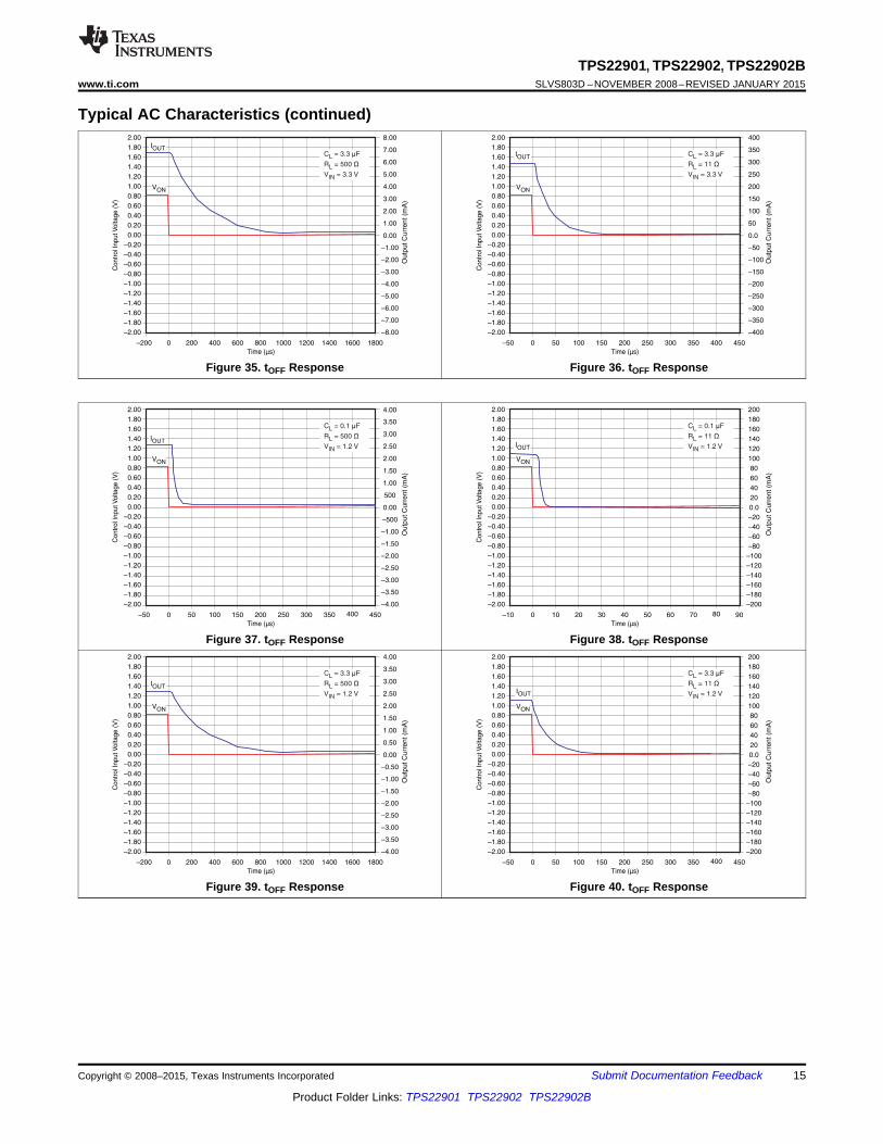
8.12.1.6 TPS22902
Figure 33. tOFF Response Figure 34. tOFF Response
14 Submit Documentation Feedback Copyright © 2008–2015, Texas Instruments Incorporated
Product Folder Links: TPS22901 TPS22902 TPS22902B
Time (µs)
Contr
ol I
nputV
olta
ge (
V)
–200 0 200 400 600 800 1000 1200 1400 18001600
2.00
1.80
1.60
–0.40
–0.60
–0.20
0.00
0.20
0.40
0.60
0.80
1.00
1.20
1.40
–2.00
–1.80
–1.00
–1.40
–1.60
–0.80
–1.20
4.00
3.50
3.00
–0.50
0.00
0.50
1.00
1.50
2.00
2.50
–4.00
–3.50
–1.50
–2.50
–3.00
–1.00
–2.00
Outp
ut C
urr
ent (m
A)
C = 3.3 F
R = 500
V = 1.2 V
L
L
IN
µ
ΩIOUT
VON
Time (µs)
Contr
ol I
nputV
olta
ge (
V)
–50 0 50 100 150 200 250 300 350 450400
2.00
1.80
1.60
–0.40
–0.60
–0.20
0.00
0.20
0.40
0.60
0.80
1.00
1.20
1.40
–2.00
–1.80
–1.00
–1.40
–1.60
–0.80
–1.20
200
180
160
–60
–40
–20
0.0
60
40
20
80
100
120
140
–200
–180
–100
–140
–160
–80
–120
Outp
ut C
urr
ent (m
A)
C = 3.3 F
R = 11
V = 1.2 V
L
L
IN
µ
ΩIOUT
VON
Time ( s)µ
Contr
ol I
nput V
olta
ge (
V)
–50 0 50 100 150 200 250 300 350 450400
2.00
1.80
1.60
–0.40
–0.60
–0.20
0.00
0.20
0.40
0.60
0.80
1.00
1.20
1.40
–2.00
–1.80
–1.00
–1.40
–1.60
–0.80
–1.20
4.00
3.50
3.00
–500
0.00
500
1.00
1.50
2.00
2.50
–4.00
–3.50
–1.50
–2.50
–3.00
–1.00
–2.00
Outp
ut C
urr
ent (m
A)
C = 0.1 F
R = 500
V = 1.2 V
L
L
IN
µ
ΩIOUT
VON
Time ( s)µ
Contr
ol I
nputV
olta
ge (
V)
–10 0 10 20 30 40 50 60 70 9080
2.00
1.80
1.60
–0.40
–0.60
–0.20
0.00
0.20
0.40
0.60
0.80
1.00
1.20
1.40
–2.00
–1.80
–1.00
–1.40
–1.60
–0.80
–1.20
200
180
160
–20
0.0
20
60
40
80
100
120
140
–200
–140
–160
–180
–60
–100
–120
–40
–80
Outp
ut C
urr
ent (m
A)
C = 0.1 F
R = 11
V = 1.2 V
L
L
IN
µ
Ω
IOUT
VON
Time (µs)
Contr
ol I
nputV
olta
ge (
V)
–200 0 200 400 600 800 1000 1200 1400 18001600
2.00
1.80
1.60
–0.40
–0.60
–0.20
0.00
0.20
0.40
0.60
0.80
1.00
1.20
1.40
–2.00
–1.80
–1.00
–1.40
–1.60
–0.80
–1.20
8.00
7.00
6.00
–1.00
0.00
1.00
2.00
3.00
4.00
5.00
–8.00
–7.00
–3.00
–5.00
–6.00
–2.00
–4.00
Outp
ut C
urr
ent (m
A)
C = 3.3 F
R = 500
V = 3.3 V
L
L
IN
µ
Ω
IOUT
VON
Time (µs)
Contr
ol I
nputV
olta
ge (
V)
2.00
1.80
1.60
–0.40
–0.60
–0.20
0.00
0.20
0.40
0.60
0.80
1.00
1.20
1.40
–2.00
–1.80
–1.00
–1.40
–1.60
–0.80
–1.20
400
350
300
–50
0.0
50
100
150
200
250
–400
–350
–150
–250
–300
–100
–200
Outp
ut C
urr
ent (m
A)
C = 3.3 F
R = 11
V = 3.3 V
L
L
IN
µ
Ω
IOUT
VON
–50 0 50 100 150 200 250 300 350 450400
TPS22901, TPS22902, TPS22902Bwww.ti.com SLVS803D –NOVEMBER 2008–REVISED JANUARY 2015
Typical AC Characteristics (continued)
Figure 35. tOFF Response Figure 36. tOFF Response
Figure 37. tOFF Response Figure 38. tOFF Response
Figure 39. tOFF Response Figure 40. tOFF Response
Copyright © 2008–2015, Texas Instruments Incorporated Submit Documentation Feedback 15
Product Folder Links: TPS22901 TPS22902 TPS22902B
Time ( s)µ
Contr
ol I
nputV
olta
ge (
V)
–1000 –500 0.0 500 1000 1500 2000 2500 3000
Outp
ut C
urr
ent (A
)
C = 0.1 F
R = 11
V = 1.2 V
L
L
IN
µ
Ω
IOUT
VON
3.5
3.2
1.2
1.0
1.4
1.6
1.8
2.0
2.2
2.4
2.6
2.8
3.0
–0.5
–0.2
0.6
0.2
0.0
0.8
0.4
0.35
0.32
0.12
0.10
0.14
0.16
0.18
0.20
0.22
0.24
0.26
0.28
0.30
–0.05
–0.02
0.06
0.02
0.00
0.08
0.04
Time ( s)µ
Contr
ol I
nput V
olta
ge (
V)
–5000 –200 0.0 200 400 600 800 12001000 1500
0.01
–0.00
0.00
Outp
ut C
urr
ent (A
)
C = 0.1 F
R = 500
V = 1.2 V
L
L
IN
µ
Ω
IOUT
VON
1.2
1.1
0.1
0.0
0.2
0.3
0.4
0.5
0.6
0.7
0.8
0.9
1.0
–0.4
–0.3
–0.2
–0.1
0.05
Time ( s)µ
Contr
ol I
nputV
olta
ge (
V)
–1000 –500 0.0 500 1000 1500 2000 2500 3000
3.5
3.2
1.2
1.0
1.4
1.6
1.8
2.0
2.2
2.4
2.6
2.8
3.0
–0.5
–0.2
0.6
0.2
0.0
0.8
0.4
0.35
0.32
0.12
0.10
0.14
0.16
0.18
0.20
0.22
0.24
0.26
0.28
0.30
–0.05
–0.02
0.06
0.02
0.00
0.08
0.04
Outp
ut C
urr
ent (A
)
C = 3 F
R = 11
V = 3.3 V
L
L
IN
µ
Ω
IOUT
VON
Time ( s)µ
Contr
ol I
nput V
olta
ge (
V)
–1000 –500 0.0 500 1000 1500 2000 2500 3000
0.01
–0.00
0.00
Outp
ut C
urr
ent (A
)
C = 3 F
R = 500
V = 3.3 V
L
L
IN
µ
Ω
IOUT
VON
1.2
1.1
0.1
0.0
0.2
0.3
0.4
0.5
0.6
0.7
0.8
0.9
1.0
–0.4
–0.3
–0.2
–0.1
0.05
Time ( s)µ
Contr
ol I
nput V
olta
ge (
V)
1.2
0.01
1.1
0.00
0.05
0.1
0.0
0.2
0.3
0.4
0.5
0.6
0.7
0.8
0.9
1.0
0.00–0.4–500 –200 0.0 200 400 600 800 1000 1200 1500
–0.3
–0.2
–0.1
C = 0.1 F
R = 500
V = 3.3 V
L
L
IN
µ
Ω
Outp
ut C
urr
ent (A
)
VON
IOUT
Time ( s)µ
Contr
ol I
nputV
olta
ge (
V)
–1000 –500 0.0 500 1000 1500 2000 2500 3000
3.5
3.2
1.2
1.0
1.4
1.6
1.8
2.0
2.2
2.4
2.6
2.8
3.0
–0.5
–0.2
0.6
0.2
0.0
0.8
0.4
0.35
0.32
0.12
0.10
0.14
0.16
0.18
0.20
0.22
0.24
0.26
0.28
0.30
–0.05
–0.02
0.06
0.02
0.00
0.08
0.04
Outp
ut C
urr
ent (A
)
C = 0.1 F
R = 11
V = 3.3 V
L
L
IN
µ
Ω
IOUT
VON
TPS22901, TPS22902, TPS22902BSLVS803D –NOVEMBER 2008–REVISED JANUARY 2015 www.ti.com
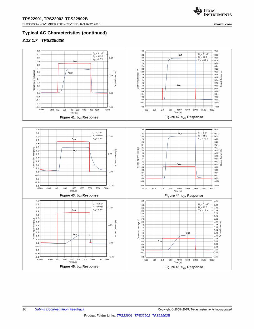
Typical AC Characteristics (continued)8.12.1.7 TPS22902B
Figure 42. tON ResponseFigure 41. tON Response
Figure 43. tON Response Figure 44. tON Response
Figure 45. tON Response Figure 46. tON Response
16 Submit Documentation Feedback Copyright © 2008–2015, Texas Instruments Incorporated
Product Folder Links: TPS22901 TPS22902 TPS22902B

Time ( s)µ
Contr
ol I
nputV
olta
ge (
V)
–250 –100 0.0 100 200 300 400 500 600 750
3.5
3.2
1.2
1.0
1.4
1.6
1.8
2.0
2.2
2.4
2.6
2.8
3.0
–0.5
–0.2
0.6
0.2
0.0
0.8
0.4
0.35
0.32
0.12
0.10
0.14
0.16
0.18
0.20
0.22
0.24
0.26
0.28
0.30
–0.05
–0.02
0.06
0.02
0.00
0.08
0.04
Outp
ut C
urr
ent (A
)
C = 3 F
R = 11
V = 3.3 V
L
L
IN
µ
ΩIOUT
VON
Time ( s)µ
Contr
ol I
nput V
olta
ge (
V)
–5000 –200 0.0 200 400 600 800 12001000 1500
0.01
–0.00
0.00
Outp
ut C
urr
ent (A
)
C = 3 F
R = 500
V = 3.3 V
L
L
IN
µ
Ω
IOUT
VON
1.2
1.1
0.1
0.0
0.2
0.3
0.4
0.5
0.6
0.7
0.8
0.9
1.0
–0.4
–0.3
–0.2
–0.1
0.05
Time ( s)µ
Contr
ol I
nputV
olta
ge (
V)
–250 –100 0.0 100 200 300 400 500 600 750
3.5
3.2
1.2
1.0
1.4
1.6
1.8
2.0
2.2
2.4
2.6
2.8
3.0
–0.5
–0.2
0.6
0.2
0.0
0.8
0.4
0.35
0.32
0.12
0.10
0.14
0.16
0.18
0.20
0.22
0.24
0.26
0.28
0.30
–0.05
–0.02
0.06
0.02
0.00
0.08
0.04
Outp
ut C
urr
ent (A
)
C = 0.1 F
R = 11
V = 3.3 V
L
L
IN
µ
ΩIOUT
VON
Time ( s)µ
Contr
ol I
nput V
olta
ge (
V)
–5000 –200 0.0 200 400 600 800 12001000 1500
0.01
–0.00
0.00
Outp
ut C
urr
ent (A
)C = 0.1 F
R = 500
V = 3.3 V
L
L
IN
µ
Ω
IOUT
VON
1.2
1.1
0.1
0.0
0.2
0.3
0.4
0.5
0.6
0.7
0.8
0.9
1.0
–0.4
–0.3
–0.2
–0.1
0.05
Time ( s)µ
Contr
ol I
nputV
olta
ge (
V)
–1000 –500 0.0 500 1000 1500 2000 2500 3000
3.5
3.2
1.2
1.0
1.4
1.6
1.8
2.0
2.2
2.4
2.6
2.8
3.0
–0.5
–0.2
0.6
0.2
0.0
0.8
0.4
0.35
0.32
0.12
0.10
0.14
0.16
0.18
0.20
0.22
0.24
0.26
0.28
0.30
–0.05
–0.02
0.06
0.02
0.00
0.08
0.04
Outp
ut C
urr
ent (A
)
C = 3 F
R = 11
V = 1.2 V
L
L
IN
µ
Ω
IOUT
VON
Time ( s)µ
Contr
ol I
nputV
olta
ge (
V)
0.01
–0.00
0.00
0.05
Outp
ut C
urr
ent (A
)
1.2
1.1
0.1
0.0
0.2
0.3
0.4
0.5
0.6
0.7
0.8
0.9
1.0
–0.4
–0.3
–0.2
–0.1
–1000 –500 0.0 500 1000 1500 2000 2500 3000
IOUT
VON
C = 3 F
R = 500
V = 1.2 V
L
L
IN
µ
Ω
TPS22901, TPS22902, TPS22902Bwww.ti.com SLVS803D –NOVEMBER 2008–REVISED JANUARY 2015
Typical AC Characteristics (continued)
Figure 47. tON Response Figure 48. tON Response
Figure 49. tOFF Response Figure 50. tOFF Response
Figure 51. tOFF Response Figure 52. tOFF Response
Copyright © 2008–2015, Texas Instruments Incorporated Submit Documentation Feedback 17
Product Folder Links: TPS22901 TPS22902 TPS22902B

Time ( s)µ
Contr
ol I
nputV
olta
ge (
V)
–250 –100 0.0 100 200 300 400 500 600 750
3.5
3.2
1.2
1.0
1.4
1.6
1.8
2.0
2.2
2.4
2.6
2.8
3.0
–0.5
–0.2
0.6
0.2
0.0
0.8
0.4
0.35
0.32
0.12
0.10
0.14
0.16
0.18
0.20
0.22
0.24
0.26
0.28
0.30
–0.05
–0.02
0.06
0.02
0.00
0.08
0.04
Outp
ut C
urr
ent (A
)
C = 3 F
R = 11
V = 1.2 V
L
L
IN
µ
Ω
IOUT
VON
Time ( s)µ
Contr
ol I
nput V
olta
ge (
V)
–1000 –500 0.0 500 1000 1500 2000 30002500
0.01
–0.00
0.00
Outp
ut C
urr
ent (A
)C = 3 F
R = 500
V = 1.2 V
L
L
IN
µ
Ω
IOUT
VON
1.2
1.1
0.1
0.0
0.2
0.3
0.4
0.5
0.6
0.7
0.8
0.9
1.0
–0.4
–0.3
–0.2
–0.1
0.05
Time ( s)µ
Contr
ol I
nputV
olta
ge (
V)
–250 –100 0.0 100 200 300 400 500 600 750
3.5
3.2
1.2
1.0
1.4
1.6
1.8
2.0
2.2
2.4
2.6
2.8
3.0
–0.5
–0.2
0.6
0.2
0.0
0.8
0.4
0.35
0.32
0.12
0.10
0.14
0.16
0.18
0.20
0.22
0.24
0.26
0.28
0.30
–0.05
–0.02
0.06
0.02
0.00
0.08
0.04
Outp
ut C
urr
ent (A
)
C = 0.1 F
R = 11
V = 1.2 V
L
L
IN
µ
Ω
IOUT
VON
Time ( s)µ
Contr
ol I
nput V
olta
ge (
V)
–50 –20 0.0 20 40 60 80 120100 150
0.01
–0.00
0.00
Outp
ut C
urr
ent (A
)
C = 0.1 F
R = 500
V = 1.2 V
L
L
IN
µ
Ω
IOUT
VON
1.2
1.1
0.1
0.0
0.2
0.3
0.4
0.5
0.6
0.7
0.8
0.9
1.0
–0.4
–0.3
–0.2
–0.1
0.05
TPS22901, TPS22902, TPS22902BSLVS803D –NOVEMBER 2008–REVISED JANUARY 2015 www.ti.com
Typical AC Characteristics (continued)
Figure 53. tOFF Response Figure 54. tOFF Response
Figure 55. tOFF Response Figure 56. tOFF Response
18 Submit Documentation Feedback Copyright © 2008–2015, Texas Instruments Incorporated
Product Folder Links: TPS22901 TPS22902 TPS22902B
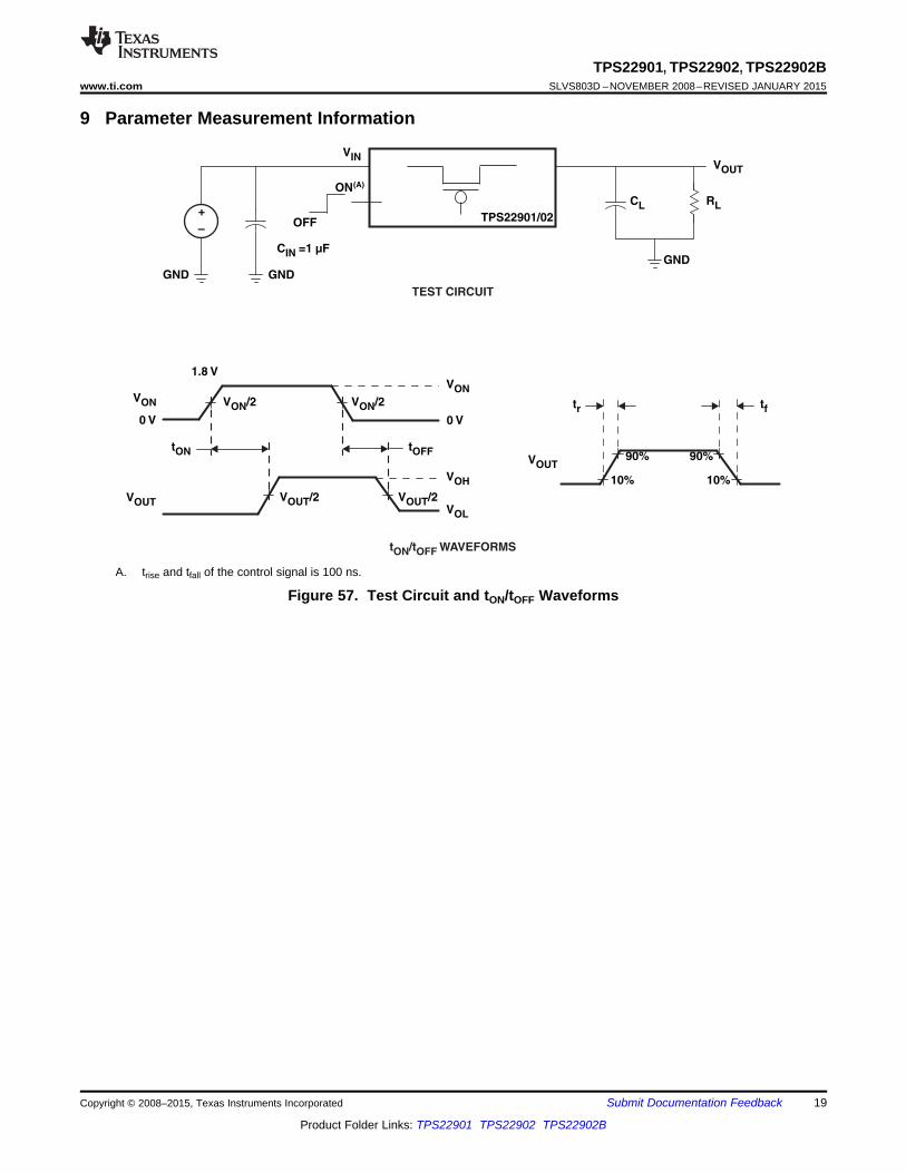
ON(A)
OFF TPS22901/02
GND
GNDGND
RLCL
VOUT
VIN
CIN =1 Fµ
+
–
90% 90%VOUT
tr tf
10%10%
V /2OUTVOUT V /2OUT
V /2ONV /2ON
VONVON
0 V0 V
1.8 V
VOH
VOL
tON tOFF
TEST CIRCUIT
t /t WAVEFORMSON OFF
TPS22901, TPS22902, TPS22902Bwww.ti.com SLVS803D –NOVEMBER 2008–REVISED JANUARY 2015
9 Parameter Measurement Information
A. trise and tfall of the control signal is 100 ns.
Figure 57. Test Circuit and tON/tOFF Waveforms
Copyright © 2008–2015, Texas Instruments Incorporated Submit Documentation Feedback 19
Product Folder Links: TPS22901 TPS22902 TPS22902B

ON
VOUT
GND
Turn-On Slew Rate
Controlled Driver
ESD Protection
VIN
ControlLogic
A2
B2
A1
B1
Output Discharge(TPS22902,TPS22902B Only)
TPS22901, TPS22902, TPS22902BSLVS803D –NOVEMBER 2008–REVISED JANUARY 2015 www.ti.com
10 Detailed Description
10.1 OverviewThe TPS2290x and TPS22902B is a single channel, 500-mA load switch in a small, space-saving DSBGA-4package. These devices implement a P-channel MOSFET to provide a low ON-resistance for a low voltage dropacross the device. A controlled rise time is used in applications to limit the inrush current.
10.2 Functional Block Diagram
10.3 Feature Description
10.3.1 ON/OFF ControlThe ON pin controls the state of the switch. Activating ON continuously holds the switch in the on state. ON isactive-high and has a low threshold, making it capable of interfacing with low-voltage signals. The ON pin iscompatible with standard GPIO logic threshold, and it can be used with any microcontroller with 1.2 V, 1.8 V, 2.5V or 3.3 V GPIOs.
10.3.2 Quick Output DischargeThe TPS2290x and TPS22902B includes the Quick Output Discharge (QOD) feature. When the switch isdisabled, a discharge resistance with a typical value of 88 Ω is connected between the output and ground. Thisresistance pulls down the output and prevents it from floating when the device is disabled.
10.4 Device Functional ModesTable 1 lists the VOURT pin connections for a particular device as determined by the ON pin.
Table 1. VOUT Function TableON (Control Input) TPS22901 TPS22902/2B
L Open GNDH VIN VIN
20 Submit Documentation Feedback Copyright © 2008–2015, Texas Instruments Incorporated
Product Folder Links: TPS22901 TPS22902 TPS22902B

ON
OFFC = 1 FIN
µ
GNDGND
GND
VOUT
LOADV
INV
BATT
RL
CLC
L
SMPS
TPS22901/02/02B(see Note A)
TPS22901, TPS22902, TPS22902Bwww.ti.com SLVS803D –NOVEMBER 2008–REVISED JANUARY 2015
11 Application and Implementation
NOTEInformation in the following applications sections is not part of the TI componentspecification, and TI does not warrant its accuracy or completeness. TI’s customers areresponsible for determining suitability of components for their purposes. Customers shouldvalidate and test their design implementation to confirm system functionality.
11.1 Application Information
11.1.1 Input Capacitor (Optional)To limit the voltage drop on the input supply caused by transient inrush currents when the switch turns on into adischarged load capacitor, a capacitor needs to be placed between VIN and GND. A 1-μF ceramic capacitor, CIN,placed close to the pins is usually sufficient. Higher values of CIN can be use to further reduce the voltage dropduring high current application. When switching heavy loads, TI recommends using an input capacitor about 10times higher than the output capacitor in order to avoid excessive voltage drop.
11.1.2 Output Capacitor (Optional)Because of the integral body diode in the PMOS switch, a CIN greater than CL is highly recommended. A CLgreater than CIN can cause VOUT to exceed VIN when the system supply is removed. This could result in currentflow through the body diode from VOUT to VIN.
11.2 Typical Application
A. Switched-mode power supply
Figure 58. Typical Application Schematic
11.2.1 Design Requirements
Table 2. Design ParametersDESIGN PARAMETER EXAMPLE VALUE
VIN 1.8 VCL 4.7 µF
Load current 500 mAAmbient Temperature 25 °C
Maximum inrush current 200 mA
Copyright © 2008–2015, Texas Instruments Incorporated Submit Documentation Feedback 21
Product Folder Links: TPS22901 TPS22902 TPS22902B
OUTINRUSH L
dVI C
dt= ´
TPS22901, TPS22902, TPS22902BSLVS803D –NOVEMBER 2008–REVISED JANUARY 2015 www.ti.com
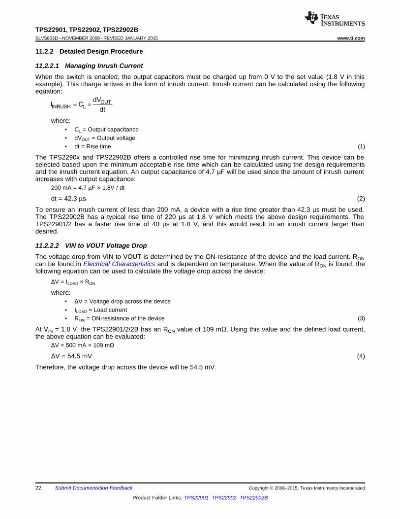
11.2.2 Detailed Design Procedure
11.2.2.1 Managing Inrush CurrentWhen the switch is enabled, the output capacitors must be charged up from 0 V to the set value (1.8 V in thisexample). This charge arrives in the form of inrush current. Inrush current can be calculated using the followingequation:
where:• CL = Output capacitance• dVOUT = Output voltage• dt = Rise time (1)
The TPS2290x and TPS22902B offers a controlled rise time for minimizing inrush current. This device can beselected based upon the minimum acceptable rise time which can be calculated using the design requirementsand the inrush current equation. An output capacitance of 4.7 µF will be used since the amount of inrush currentincreases with output capacitance:
200 mA = 4.7 µF × 1.8V / dt
dt = 42.3 µs (2)
To ensure an inrush current of less than 200 mA, a device with a rise time greater than 42.3 µs must be used.The TPS22902B has a typical rise time of 220 µs at 1.8 V which meets the above design requirements. TheTPS22901/2 has a faster rise time of 40 µs at 1.8 V, and this would result in an inrush current larger thandesired.
11.2.2.2 VIN to VOUT Voltage DropThe voltage drop from VIN to VOUT is determined by the ON-resistance of the device and the load current. RONcan be found in Electrical Characteristics and is dependent on temperature. When the value of RON is found, thefollowing equation can be used to calculate the voltage drop across the device:
ΔV = ILOAD × RON
where:• ΔV = Voltage drop across the device• ILOAD = Load current• RON = ON-resistance of the device (3)
At VIN = 1.8 V, the TPS22901/2/2B has an RON value of 109 mΩ. Using this value and the defined load current,the above equation can be evaluated:
ΔV = 500 mA × 109 mΩ
ΔV = 54.5 mV (4)
Therefore, the voltage drop across the device will be 54.5 mV.
22 Submit Documentation Feedback Copyright © 2008–2015, Texas Instruments Incorporated
Product Folder Links: TPS22901 TPS22902 TPS22902B
0.00 0.05 0.10 0.15 0.20 0.25 0.30 0.35 0.40 0.45 0.50
Load Current (A)
0
10
20
30
40
50
60
70
80
90
100
Voltage D
rop (
mV
) V = 1.0 Vdrop
V = 1.2 Vdrop
V = 1.8 Vdrop
V = 2.5 Vdrop
V = 3.3 Vdrop
TPS22901, TPS22902, TPS22902Bwww.ti.com SLVS803D –NOVEMBER 2008–REVISED JANUARY 2015
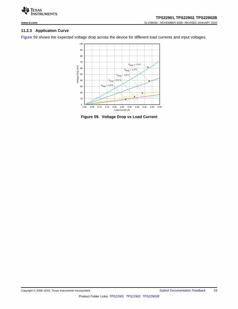
11.2.3 Application CurveFigure 59 shows the expected voltage drop across the device for different load currents and input voltages.
Figure 59. Voltage Drop vs Load Current
Copyright © 2008–2015, Texas Instruments Incorporated Submit Documentation Feedback 23
Product Folder Links: TPS22901 TPS22902 TPS22902B
TPS22901, TPS22902, TPS22902BSLVS803D –NOVEMBER 2008–REVISED JANUARY 2015 www.ti.com
12 Power Supply Recommendations
The device is designed to operate with a VIN range of 1 V to 3.6 V. This supply must be well regulated andplaced as close to the device terminals as possible. It must also be able to withstand all transient and loadcurrents, using a recommended input capacitance of 1 µF if necessary. If the supply is located more than a fewinches from the device terminals, additional bulk capacitance may be required in addition to the ceramic bypasscapacitors. If additional bulk capacitance is required, an electrolytic, tantalum, or ceramic capacitor of 10 µF maybe sufficient.
13 Layout
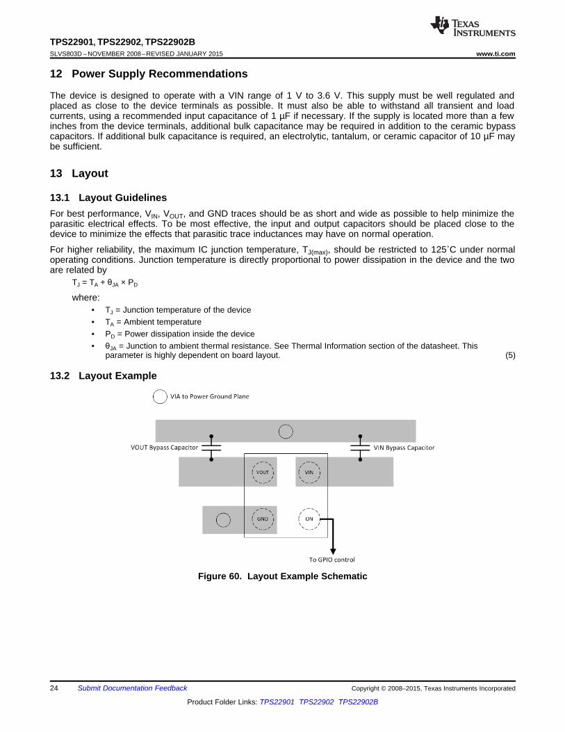
13.1 Layout GuidelinesFor best performance, VIN, VOUT, and GND traces should be as short and wide as possible to help minimize theparasitic electrical effects. To be most effective, the input and output capacitors should be placed close to thedevice to minimize the effects that parasitic trace inductances may have on normal operation.
For higher reliability, the maximum IC junction temperature, TJ(max), should be restricted to 125˚C under normaloperating conditions. Junction temperature is directly proportional to power dissipation in the device and the twoare related by
TJ = TA + θJA × PD
where:• TJ = Junction temperature of the device• TA = Ambient temperature• PD = Power dissipation inside the device• θJA = Junction to ambient thermal resistance. See Thermal Information section of the datasheet. This
parameter is highly dependent on board layout. (5)
13.2 Layout Example
Figure 60. Layout Example Schematic
24 Submit Documentation Feedback Copyright © 2008–2015, Texas Instruments Incorporated
Product Folder Links: TPS22901 TPS22902 TPS22902B

TPS22901, TPS22902, TPS22902Bwww.ti.com SLVS803D –NOVEMBER 2008–REVISED JANUARY 2015
14 Device and Documentation Support
14.1 Related LinksThe table below lists quick access links. Categories include technical documents, support and communityresources, tools and software, and quick access to sample or buy.
Table 3. Related LinksTECHNICAL TOOLS & SUPPORT &PARTS PRODUCT FOLDER SAMPLE & BUY DOCUMENTS SOFTWARE COMMUNITY
TPS22901 Click here Click here Click here Click here Click hereTPS22902 Click here Click here Click here Click here Click here
TPS22902B Click here Click here Click here Click here Click here
14.2 TrademarksAll trademarks are the property of their respective owners.
14.3 Electrostatic Discharge CautionThese devices have limited built-in ESD protection. The leads should be shorted together or the device placed in conductive foamduring storage or handling to prevent electrostatic damage to the MOS gates.
14.4 GlossarySLYZ022 — TI Glossary.
This glossary lists and explains terms, acronyms, and definitions.
15 Mechanical, Packaging, and Orderable InformationThe following pages include mechanical, packaging, and orderable information. This information is the mostcurrent data available for the designated devices. This data is subject to change without notice and revision ofthis document. For browser-based versions of this data sheet, refer to the left-hand navigation.
Copyright © 2008–2015, Texas Instruments Incorporated Submit Documentation Feedback 25
Product Folder Links: TPS22901 TPS22902 TPS22902B

PACKAGE OPTION ADDENDUM
www.ti.com 25-Oct-2016
Addendum-Page 1
PACKAGING INFORMATION
Orderable Device Status(1)
Package Type PackageDrawing
Pins PackageQty
Eco Plan(2)
Lead/Ball Finish(6)
MSL Peak Temp(3)
Op Temp (°C) Device Marking(4/5)
Samples
TPS22901YFPR ACTIVE DSBGA YFP 4 3000 Green (RoHS& no Sb/Br)
SNAGCU Level-1-260C-UNLIM -40 to 85 3P(3 ~ 5)
TPS22902BYFPR ACTIVE DSBGA YFP 4 3000 Green (RoHS& no Sb/Br)
SNAGCU Level-1-260C-UNLIM -40 to 85 3S3
TPS22902YFPR ACTIVE DSBGA YFP 4 3000 Green (RoHS& no Sb/Br)
SNAGCU Level-1-260C-UNLIM -40 to 85 3R
(1) The marketing status values are defined as follows:ACTIVE: Product device recommended for new designs.LIFEBUY: TI has announced that the device will be discontinued, and a lifetime-buy period is in effect.NRND: Not recommended for new designs. Device is in production to support existing customers, but TI does not recommend using this part in a new design.PREVIEW: Device has been announced but is not in production. Samples may or may not be available.OBSOLETE: TI has discontinued the production of the device.
(2) Eco Plan - The planned eco-friendly classification: Pb-Free (RoHS), Pb-Free (RoHS Exempt), or Green (RoHS & no Sb/Br) - please check http://www.ti.com/productcontent for the latest availabilityinformation and additional product content details.TBD: The Pb-Free/Green conversion plan has not been defined.Pb-Free (RoHS): TI's terms "Lead-Free" or "Pb-Free" mean semiconductor products that are compatible with the current RoHS requirements for all 6 substances, including the requirement thatlead not exceed 0.1% by weight in homogeneous materials. Where designed to be soldered at high temperatures, TI Pb-Free products are suitable for use in specified lead-free processes.Pb-Free (RoHS Exempt): This component has a RoHS exemption for either 1) lead-based flip-chip solder bumps used between the die and package, or 2) lead-based die adhesive used betweenthe die and leadframe. The component is otherwise considered Pb-Free (RoHS compatible) as defined above.Green (RoHS & no Sb/Br): TI defines "Green" to mean Pb-Free (RoHS compatible), and free of Bromine (Br) and Antimony (Sb) based flame retardants (Br or Sb do not exceed 0.1% by weightin homogeneous material)
(3) MSL, Peak Temp. - The Moisture Sensitivity Level rating according to the JEDEC industry standard classifications, and peak solder temperature.
(4) There may be additional marking, which relates to the logo, the lot trace code information, or the environmental category on the device.
(5) Multiple Device Markings will be inside parentheses. Only one Device Marking contained in parentheses and separated by a "~" will appear on a device. If a line is indented then it is a continuationof the previous line and the two combined represent the entire Device Marking for that device.
(6) Lead/Ball Finish - Orderable Devices may have multiple material finish options. Finish options are separated by a vertical ruled line. Lead/Ball Finish values may wrap to two lines if the finishvalue exceeds the maximum column width.
Important Information and Disclaimer:The information provided on this page represents TI's knowledge and belief as of the date that it is provided. TI bases its knowledge and belief on informationprovided by third parties, and makes no representation or warranty as to the accuracy of such information. Efforts are underway to better integrate information from third parties. TI has taken and

PACKAGE OPTION ADDENDUM
www.ti.com 25-Oct-2016
Addendum-Page 2
continues to take reasonable steps to provide representative and accurate information but may not have conducted destructive testing or chemical analysis on incoming materials and chemicals.TI and TI suppliers consider certain information to be proprietary, and thus CAS numbers and other limited information may not be available for release.
In no event shall TI's liability arising out of such information exceed the total purchase price of the TI part(s) at issue in this document sold by TI to Customer on an annual basis.
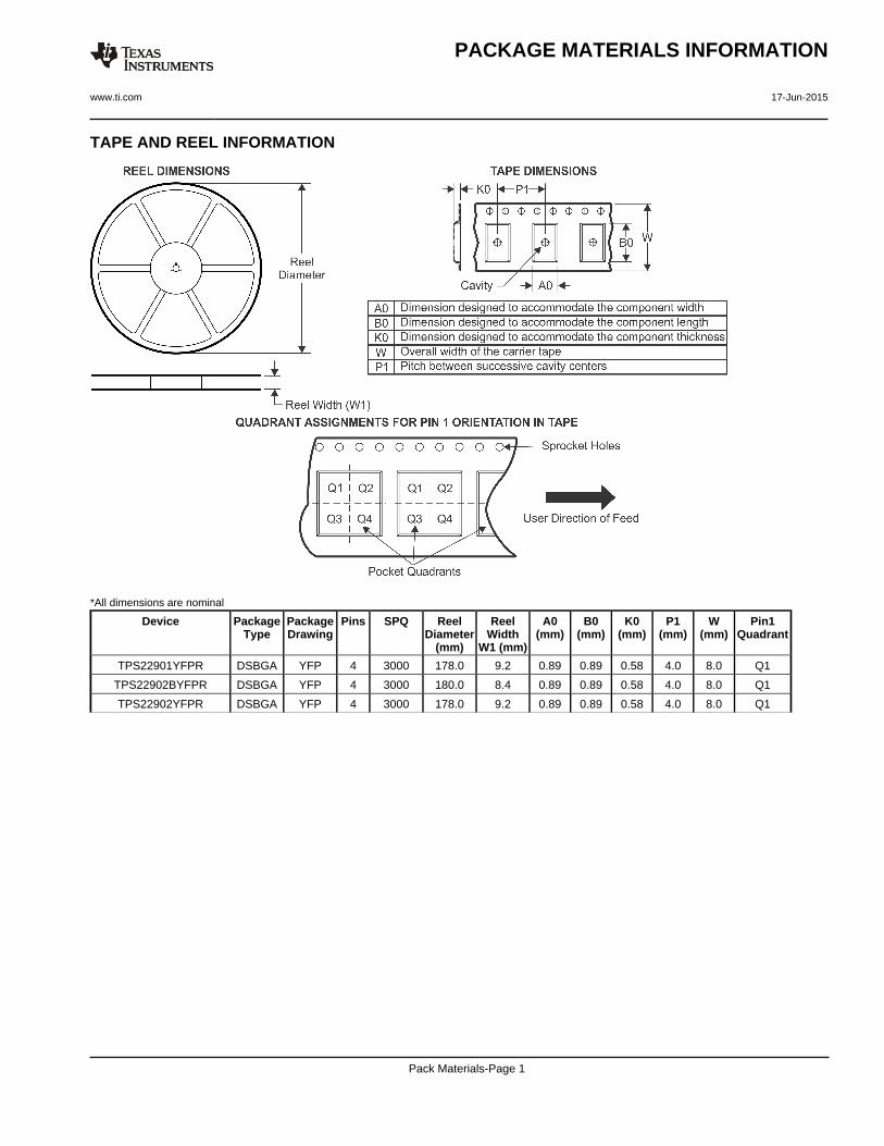
TAPE AND REEL INFORMATION
*All dimensions are nominal
Device PackageType
PackageDrawing
Pins SPQ ReelDiameter
(mm)
ReelWidth
W1 (mm)
A0(mm)
B0(mm)
K0(mm)
P1(mm)
W(mm)
Pin1Quadrant
TPS22901YFPR DSBGA YFP 4 3000 178.0 9.2 0.89 0.89 0.58 4.0 8.0 Q1
TPS22902BYFPR DSBGA YFP 4 3000 180.0 8.4 0.89 0.89 0.58 4.0 8.0 Q1
TPS22902YFPR DSBGA YFP 4 3000 178.0 9.2 0.89 0.89 0.58 4.0 8.0 Q1
PACKAGE MATERIALS INFORMATION
www.ti.com 17-Jun-2015
Pack Materials-Page 1

*All dimensions are nominal
Device Package Type Package Drawing Pins SPQ Length (mm) Width (mm) Height (mm)
TPS22901YFPR DSBGA YFP 4 3000 220.0 220.0 35.0
TPS22902BYFPR DSBGA YFP 4 3000 182.0 182.0 20.0
TPS22902YFPR DSBGA YFP 4 3000 270.0 225.0 227.0
PACKAGE MATERIALS INFORMATION
www.ti.com 17-Jun-2015
Pack Materials-Page 2

www.ti.com
PACKAGE OUTLINE
C0.5 MAX
0.190.13
0.4TYP
0.4TYP
4X 0.250.21
B E A
D
4223507/A 01/2017
DSBGA - 0.5 mm max heightYFP0004DIE SIZE BALL GRID ARRAY
NOTES: 1. All linear dimensions are in millimeters. Any dimensions in parenthesis are for reference only. Dimensioning and tolerancing per ASME Y14.5M. 2. This drawing is subject to change without notice.
BALL A1CORNER
SEATING PLANE
BALL TYP 0.05 C
A
B
20.015 C A B
SYMM
SYMM
1
SCALE 10.000
D: Max =
E: Max =
0.79 mm, Min =
0.79 mm, Min =
0.73 mm
0.73 mm

www.ti.com
EXAMPLE BOARD LAYOUT
4X ( 0.23)
(0.4) TYP
(0.4) TYP
( 0.23)METAL
0.05 MAX
SOLDER MASKOPENING
METAL UNDERSOLDER MASK
( 0.23)SOLDER MASKOPENING
0.05 MIN
4223507/A 01/2017
DSBGA - 0.5 mm max heightYFP0004DIE SIZE BALL GRID ARRAY
NOTES: (continued) 3. Final dimensions may vary due to manufacturing tolerance considerations and also routing constraints. For more information, see Texas Instruments literature number SNVA009 (www.ti.com/lit/snva009).
SOLDER MASK DETAILSNOT TO SCALE
SYMM
SYMM
LAND PATTERN EXAMPLEEXPOSED METAL SHOWN
SCALE:50X
A
B
1 2
NON-SOLDER MASKDEFINED
(PREFERRED)
EXPOSEDMETAL
SOLDER MASKDEFINED
EXPOSEDMETAL

www.ti.com
EXAMPLE STENCIL DESIGN
(0.4) TYP
(0.4) TYP
4X ( 0.25) (R0.05) TYP
METALTYP
4223507/A 01/2017
DSBGA - 0.5 mm max heightYFP0004DIE SIZE BALL GRID ARRAY
NOTES: (continued) 4. Laser cutting apertures with trapezoidal walls and rounded corners may offer better paste release.
SYMM
SYMM
SOLDER PASTE EXAMPLEBASED ON 0.1 mm THICK STENCIL
SCALE:50X
A
B
1 2
IMPORTANT NOTICE
Texas Instruments Incorporated (TI) reserves the right to make corrections, enhancements, improvements and other changes to itssemiconductor products and services per JESD46, latest issue, and to discontinue any product or service per JESD48, latest issue. Buyersshould obtain the latest relevant information before placing orders and should verify that such information is current and complete.TI’s published terms of sale for semiconductor products (http://www.ti.com/sc/docs/stdterms.htm) apply to the sale of packaged integratedcircuit products that TI has qualified and released to market. Additional terms may apply to the use or sale of other types of TI products andservices.Reproduction of significant portions of TI information in TI data sheets is permissible only if reproduction is without alteration and isaccompanied by all associated warranties, conditions, limitations, and notices. TI is not responsible or liable for such reproduceddocumentation. Information of third parties may be subject to additional restrictions. Resale of TI products or services with statementsdifferent from or beyond the parameters stated by TI for that product or service voids all express and any implied warranties for theassociated TI product or service and is an unfair and deceptive business practice. TI is not responsible or liable for any such statements.Buyers and others who are developing systems that incorporate TI products (collectively, “Designers”) understand and agree that Designersremain responsible for using their independent analysis, evaluation and judgment in designing their applications and that Designers havefull and exclusive responsibility to assure the safety of Designers' applications and compliance of their applications (and of all TI productsused in or for Designers’ applications) with all applicable regulations, laws and other applicable requirements. Designer represents that, withrespect to their applications, Designer has all the necessary expertise to create and implement safeguards that (1) anticipate dangerousconsequences of failures, (2) monitor failures and their consequences, and (3) lessen the likelihood of failures that might cause harm andtake appropriate actions. Designer agrees that prior to using or distributing any applications that include TI products, Designer willthoroughly test such applications and the functionality of such TI products as used in such applications.TI’s provision of technical, application or other design advice, quality characterization, reliability data or other services or information,including, but not limited to, reference designs and materials relating to evaluation modules, (collectively, “TI Resources”) are intended toassist designers who are developing applications that incorporate TI products; by downloading, accessing or using TI Resources in anyway, Designer (individually or, if Designer is acting on behalf of a company, Designer’s company) agrees to use any particular TI Resourcesolely for this purpose and subject to the terms of this Notice.TI’s provision of TI Resources does not expand or otherwise alter TI’s applicable published warranties or warranty disclaimers for TIproducts, and no additional obligations or liabilities arise from TI providing such TI Resources. TI reserves the right to make corrections,enhancements, improvements and other changes to its TI Resources. TI has not conducted any testing other than that specificallydescribed in the published documentation for a particular TI Resource.Designer is authorized to use, copy and modify any individual TI Resource only in connection with the development of applications thatinclude the TI product(s) identified in such TI Resource. NO OTHER LICENSE, EXPRESS OR IMPLIED, BY ESTOPPEL OR OTHERWISETO ANY OTHER TI INTELLECTUAL PROPERTY RIGHT, AND NO LICENSE TO ANY TECHNOLOGY OR INTELLECTUAL PROPERTYRIGHT OF TI OR ANY THIRD PARTY IS GRANTED HEREIN, including but not limited to any patent right, copyright, mask work right, orother intellectual property right relating to any combination, machine, or process in which TI products or services are used. Informationregarding or referencing third-party products or services does not constitute a license to use such products or services, or a warranty orendorsement thereof. Use of TI Resources may require a license from a third party under the patents or other intellectual property of thethird party, or a license from TI under the patents or other intellectual property of TI.TI RESOURCES ARE PROVIDED “AS IS” AND WITH ALL FAULTS. TI DISCLAIMS ALL OTHER WARRANTIES ORREPRESENTATIONS, EXPRESS OR IMPLIED, REGARDING RESOURCES OR USE THEREOF, INCLUDING BUT NOT LIMITED TOACCURACY OR COMPLETENESS, TITLE, ANY EPIDEMIC FAILURE WARRANTY AND ANY IMPLIED WARRANTIES OFMERCHANTABILITY, FITNESS FOR A PARTICULAR PURPOSE, AND NON-INFRINGEMENT OF ANY THIRD PARTY INTELLECTUALPROPERTY RIGHTS. TI SHALL NOT BE LIABLE FOR AND SHALL NOT DEFEND OR INDEMNIFY DESIGNER AGAINST ANY CLAIM,INCLUDING BUT NOT LIMITED TO ANY INFRINGEMENT CLAIM THAT RELATES TO OR IS BASED ON ANY COMBINATION OFPRODUCTS EVEN IF DESCRIBED IN TI RESOURCES OR OTHERWISE. IN NO EVENT SHALL TI BE LIABLE FOR ANY ACTUAL,DIRECT, SPECIAL, COLLATERAL, INDIRECT, PUNITIVE, INCIDENTAL, CONSEQUENTIAL OR EXEMPLARY DAMAGES INCONNECTION WITH OR ARISING OUT OF TI RESOURCES OR USE THEREOF, AND REGARDLESS OF WHETHER TI HAS BEENADVISED OF THE POSSIBILITY OF SUCH DAMAGES.Unless TI has explicitly designated an individual product as meeting the requirements of a particular industry standard (e.g., ISO/TS 16949and ISO 26262), TI is not responsible for any failure to meet such industry standard requirements.Where TI specifically promotes products as facilitating functional safety or as compliant with industry functional safety standards, suchproducts are intended to help enable customers to design and create their own applications that meet applicable functional safety standardsand requirements. Using products in an application does not by itself establish any safety features in the application. Designers mustensure compliance with safety-related requirements and standards applicable to their applications. Designer may not use any TI products inlife-critical medical equipment unless authorized officers of the parties have executed a special contract specifically governing such use.Life-critical medical equipment is medical equipment where failure of such equipment would cause serious bodily injury or death (e.g., lifesupport, pacemakers, defibrillators, heart pumps, neurostimulators, and implantables). Such equipment includes, without limitation, allmedical devices identified by the U.S. Food and Drug Administration as Class III devices and equivalent classifications outside the U.S.TI may expressly designate certain products as completing a particular qualification (e.g., Q100, Military Grade, or Enhanced Product).Designers agree that it has the necessary expertise to select the product with the appropriate qualification designation for their applicationsand that proper product selection is at Designers’ own risk. Designers are solely responsible for compliance with all legal and regulatoryrequirements in connection with such selection.Designer will fully indemnify TI and its representatives against any damages, costs, losses, and/or liabilities arising out of Designer’s non-compliance with the terms and provisions of this Notice.
Mailing Address: Texas Instruments, Post Office Box 655303, Dallas, Texas 75265Copyright © 2017, Texas Instruments Incorporated