sllseb7 – may 2012 11.3 gbps modulator driver circuit boards. ... a simplified block diagram of...
TRANSCRIPT

ONET1141Lwww.ti.com SLLSEB7 –MAY 2012
11.3 Gbps Modulator DriverCheck for Samples: ONET1141L
1FEATURES • Includes Laser Safety Features• Single 3.3V Supply• Digitally Selectable Output Amplitude up to
2.0VPP Single-Ended • –40°C to 100°C Operation• Digitally Selectable Bias Current up to 145mA • Surface Mount Small Footprint 4mm × 4mm 24
Source Pin RoHS Compliant QFN Package• 2-wire Digital Interface with Integrated DACs
APPLICATIONSand ADC for Control and DiagnosticManagement • 10 Gigabit Ethernet Optical Transmitters
• Automatic Power Control (APC) Loop • SONET OC-192/SDH STM-64 Optical• Adjustable Rise and Fall Times Transmitters• Programmable Input Equalizer • 10G-EPON and XG-PON• Cross-Point Control • SFP+ and XFP Transceiver Modules• Selectable Monitor PD Current Range and • XENPAK, XPAK, X2 and 300-pin MSA
Polarity Transponder Modules
DESCRIPTIONThe ONET1141L is a high-speed, 3.3V electroabsorption modulator driver designed to bias and modulate anelectroabsorptive modulated laser (EML) at data rates from 1 Gbps up to 11.3 Gbps.
The device provides a two-wire serial interface which allows digital control of the modulation and bias currents,eliminating the need for external components. Output waveform control, in the form of cross-point adjustmentand rise and fall time adjustment are available to improve the optical eye mask margin. An optional inputequalizer can be used for equalization of up to 150mm (6”) of microstrip or stripline transmission line on FR4printed circuit boards. The device contains internal analog to digital and digital to analog converters to eliminatethe need for special purpose microcontrollers.
The ONET1141L includes an integrated automatic power control (APC) loop which compensates for variations inlaser average optical power over voltage and temperature and circuitry to support laser safety and transceivermanagement systems.
The modulator driver is characterized for operation from –40°C to 100°C case temperatures and is available in asmall footprint 4mm × 4mm 24 pin RoHS compliant QFN package.
1
Please be aware that an important notice concerning availability, standard warranty, and use in critical applications ofTexas Instruments semiconductor products and disclaimers thereto appears at the end of this data sheet.
PRODUCTION DATA information is current as of publication date. Copyright © 2012, Texas Instruments IncorporatedProducts conform to specifications per the terms of the TexasInstruments standard warranty. Production processing does notnecessarily include testing of all parameters.

Limiter
5 Bit Register
Crosspoint
IMOD
IBIAS
Settings
Crosspoint
Adjust
Crosspoint Adjust
Power-On
Reset
Band-Gap, Analog References,
Power supply Monitor &
Temperature Sensor
Bias
Current
Generator/
Monitor &
APC
2-Wire Interface & Control Logic
SDA
SCK
DIS
PD
FLT
BIAS
DIN+
DIN-
BIAS
FLT
PD
RZTCRZTC
Settings
8 Bit Register
8 Bit Register
10 Bit Register
10 Bit Register
8 Bit Register
Crosspoint Settings
ADC Settings
10 Bit Register
8 Bit Register
ADC
Analog to
Digital
Conversion
DC Offset Cancellation
Adjustable
Boost
8 Bit Register
Equalizer
MONB
MONP
PSM
TS
SDA
SCK
DIS
VCC
10kΩ10kΩ10kΩ
COMPCOMP
Limiter Current
8 Bit Register
60Ω
MONB MONB
MONP MONP
OUT+
OUT-
Mod.
Current
Generator
60Ω
Equalizer
+
+
Bypass
ADR1
ADR2
ADR0
ADR1
8 Bit Register Bias Current Fault
Amplifier100Ω
3 Bit Register Monitor Settings
8 Bit Register PD Current Fault
VCCO
VCC To all Blocks Except Output Driver
ONET1141LSLLSEB7 –MAY 2012 www.ti.com
These devices have limited built-in ESD protection. The leads should be shorted together or the device placed in conductive foamduring storage or handling to prevent electrostatic damage to the MOS gates.
BLOCK DIAGRAM
A simplified block diagram of the ONET1141L is shown in Figure 1. The modulator driver consists of an inputequalizer with selectable bypass, a limiter, an output driver, DC offset cancellation with cross point control,power-on reset circuitry, a 2-wire serial interface including a control logic block, a modulation current generator, abias current generator with automatic power control loop, an analog to digital converter and an analog referenceblock.
Figure 1. Simplified Block Diagram of the ONET1141L
PACKAGE
The ONET1141L is packaged in a small footprint 4mm X 4mm 24 pin RoHS compliant QFN package with a leadpitch of 0.5mm. The pin out is shown below.
2 Submit Documentation Feedback Copyright © 2012, Texas Instruments Incorporated
Product Folder Link(s) :ONET1141L

PD
ADR0
ADR1
DIS
SDA
SCK
2
1
3
4
5
6
17
18
16
15
14
13
87 9 10 11 12
2324 22 21 20 19
BIAS
GND
VCC
COMP
MONB
MONP
VC
CO
GN
D
OU
T+
OU
T-
VC
CO
GN
D
GN
D
DIN
+
DIN
-
GN
D
RZ
TC
FL
T
ONET1101L
24 Lead QFN
“ RGE”
ONET1141L
24Lead QFN
ONET1141Lwww.ti.com SLLSEB7 –MAY 2012
24 PIN QFN PACKAGE, 4mm x 4mm(TOP VIEW)
PIN FUNCTIONSNO.
TYPE DESCRIPTIONPIN NAME
1 PD Analog Photodiode input. Pin can source or sink current dependent on register setting.
2 ADR0 Digital-in 2-wire interface address programming pin. Leave this pad open for a default address of 0001000.Pulling the pin to VCC changes the 1st address bit to a 1 (address = 0001001)
3 ADR1 Digital-in 2-wire interface address programming pin. Leave this pad open for a default address of 0001000.Pulling the pin to VCC changes the 2nd address bit to a 1 (address = 0001010)
4 DIS Digital-in Disables both bias and modulation currents when set to high state. Includes a 10kΩ or 40kΩ pull-upresistor to VCC. Toggle to reset a fault condition.
5 SCK Digital-in 2-wire interface serial clock input. Includes a 10kΩ or 40kΩ pull-up resistor to VCC.
6 SDA Digital-in/out 2-wire interface serial data input/output. Includes a 10kΩ or 40kΩ pull-up resistor to VCC.
7 FLT Digital-out Fault detection flag. High level indicates that a fault has occurred. Open drain output. Requires anexternal 4.7kΩ to 10kΩ pull-up resistor to VCC for proper operation.
8, 11, 17, GND Supply Circuit ground. Exposed die pad (EP) must be grounded.20, 23, EP
9 DIN+ Analog-in Non-inverted data input. On-chip differentially 100Ω terminated to DIN–. Must be AC coupled.
10 DIN– Analog-in Inverted data input. On-chip differentially 100Ω terminated to DIN+. Must be AC coupled.
12 RZTC Analog Connect external zero TC 28.7kΩ resistor to ground (GND). Used to generate a defined zero TCreference current for internal DACs.
13 MONB Analog-out Bias current monitor. Sources a 1% replica of the bias current. Connect an external resistor toground (GND) to use the analog monitor (DMONB = 0). If the voltage at this pin exceeds 1.16V afault is triggered. Typically choose a resistor to give MONB voltage of 0.8V at the maximum desiredbias current. If the digital monitor function is used (DMONB = 1) the resistor must be removed.
14 MONP Analog-out Photodiode current monitor. Sources a 12.5% replica of the photodiode current when PDRNG = 1X,a 25% replica when PDRNG = 01 and a 50% replica when PDRNG = 00. Connect an externalresistor (5kΩ typical) to ground (GND) to use the analog monitor (DMONP = 0). If the voltage at thispin exceeds 1.16V a fault is triggered when MONPFLT = 1. If the digital monitor function is used(DMONP = 1) the resistor must be removed.
15 COMP Analog Compensation pin used to control the bandwidth of the APC loop. Connect a 0.01µF capacitor toground.
16 VCC Supply 3.3V ± 10% supply voltage.
18 BIAS Analog Sinks or sources the bias current for the laser in both APC and open loop modes.
19, 24 VCCO Supply 3.3V ± 10% supply voltage for the output stage.
21 OUT– CML-out Inverted data output.
22 OUT+ CML-out Non-inverted data output.
Copyright © 2012, Texas Instruments Incorporated Submit Documentation Feedback 3
Product Folder Link(s) :ONET1141L

ONET1141LSLLSEB7 –MAY 2012 www.ti.com
ABSOLUTE MAXIMUM RATINGSover operating free-air temperature range (unless otherwise noted) (1)
VALUE UNIT
MIN MAX
VCC Supply voltage (2) –0.3 4.0 V
VADR0, VADR1, VDIS, VRZTC,VSCK, VSDA, VDIN+, VDIN-, VFLT, Voltage at ADR0, ADR1, DIS, RZTC, SCK, SDA, DIN+, DIN–, FLT, MONB, –0.3 4.0 VVMONB, VMONP, VCOMP, VPD, MONP, COMP, PD, BIAS, OUT+, OUT– (2)
VBIAS, VOUT+, VOUT-
IDIN-, IDIN+ Maximum current at input pins 25 mA
IOUT+, IOUT– Maximum current at output pins 120 mA
IBIAS-MAX Maximum bias current 180 mA
ESD ESD rating at all pins 2 kV (HBM)
TJ,max Maximum junction temperature 125 °C
TSTG Storage temperature range –65 150 °C
TC Case temperature –40 110 °C
(1) Stresses beyond those listed under “absolute maximum ratings” may cause permanent damage to the device. These are stress ratingsonly, and functional operation of the device at these or any other conditions beyond those indicated under “recommended operatingconditions” is not implied. Exposure to absolute–maximum–rated conditions for extended periods may affect device reliability.
(2) All voltage values are with respect to network ground terminal.
RECOMMENDED OPERATING CONDITIONSover operating free-air temperature range (unless otherwise noted)
MIN TYP MAX UNIT
VCC Supply voltage 2.97 3.3 3.63 V
VIH Digital input high voltage DIS, SCK, SDA 2.0 V
VIL Digital input low voltage DIS, SCK, SDA 0.8 V
Control bit PDRNG = 1X,step size = 3 µA 3080
Photodiode current range Control bit PDRNG = 01,step size = 1.5 µA 1540 µA
Control bit PDRNG = 00,step size = 0.75 µA 770
RRZTC Zero TC resistor value (1) 1.16V bandgap bias acrossresistor, E96, 1% accuracy 28.4 28.7 29 kΩEQENA = 1 160 1000
vIN Differential input voltage swing mVp-pEQENA = 0 400 1000
tR-IN Input rise time 20%–80% 30 55 ps
tF-IN Input fall time 20%–80% 30 55 ps
TC Temperature at thermal pad -40 100 °C
(1) Changing the value will alter the DAC ranges.
4 Submit Documentation Feedback Copyright © 2012, Texas Instruments Incorporated
Product Folder Link(s) :ONET1141L

ONET1141Lwww.ti.com SLLSEB7 –MAY 2012
DC ELECTRICAL CHARACTERISTICSOver recommended operating conditions, with 50Ω output load, open loop operation, VOUT = 2.0Vpp, IBIAS = 80 mA, and RRZTC
= 28.7kΩ unless otherwise noted. Typical operating condition is at VCC =3.3V and TA = 25°C
PARAMETER CONDITION MIN TYP MAX UNIT
VCC Supply voltage 2.97 3.3 3.63 V
VOUT = 2.0Vpp, IBIAS = 0mA, EQENA = 0 143 170
VOUT = 2.0Vpp, IBIAS = 0mA, EQENA = 1 151 182IVCC Supply current mA
Output off (DIS = HIGH), VOUT = 2.0Vpp,40
IBIAS = 80 mA, EQENA = 0
RIN Data input resistance Differential between DIN+ / DIN– 82 100 118 ΩROUT Output resistance Single-ended at OUT+ or OUT– 50 60 70 Ω
Digital input current SCK, SDA, pull up to VCC 2 360 470 µA
Digital input current DIS, pull up to VCC 2 360 470 µA
VOH Digital output high voltage FLT, pull-up to VCC, ISOURCE = 50 µA 2.4 V
VOL Digital output low voltage FLT, pull-up to VCC, ISINK = 350 µA 0.4 V
IBIAS-MIN Minimum bias current See (1) 5 mA
Source. BIASPOL = 0, DAC set to maximum, open 145 160and closed loopIBIAS-MAX Maximum bias current mA
Sink. BIASPOL = 1, DAC set to maximum, open and 93 105closed loop
IBIAS-DIS Bias current during disable 100 µA
Average power stability APC loop enabled ±0.5 dB
Bias pin compliance voltage Source. BIASPOL = 0 0.9 V
Sink. BIASPOL = 1 VCC–0.9
Temperature sensor accuracy With 1-point external mid scale calibration ±3 °C
Photodiode reverse biasVPD APC active, IPD = max 1.3 2.3 Vvoltage
Photodiode fault current level Percent of target IPD(2) 150%
IMONP / IPD with control bit PDRNG = 1X 10% 12.5% 15%Photodiode current monitor IMONP / IPD with control bit PDRNG = 01 20% 25% 30%ratio
IMONP / IPD with control bit PDRNG = 00 40% 50% 60%
Monitor diode DMI accuracy With external calibration at 200 µA -10% 10%
Bias current monitor ratio IMONB / IBIAS (nominal 1/100 = 1%) 0.9% 1.0% 1.1%
Bias current DMI accuracy Bias current ≥ 30 mA ±10%
Power supply monitor With external mid scale calibration –2% 2%accuracy
VCC-RST VCC reset threshold voltage VCC voltage level which triggers power-on reset 2.5 2.8 V
VCC reset threshold voltageVCC-RSTHYS 100 mVhysteresis
VMONB-FLT Fault voltage at MONB Fault occurs if voltage at MONB exceeds value 1.1 1.16 1.24 V
(1) The bias current can be set below the specified minimum according to the corresponding register setting, however in closed loopoperation settings below the specified value may trigger a fault.
(2) Assured by simulation over process, supply and temperature variation.
Copyright © 2012, Texas Instruments Incorporated Submit Documentation Feedback 5
Product Folder Link(s) :ONET1141L

ONET1141LSLLSEB7 –MAY 2012 www.ti.com
AC ELECTRICAL CHARACTERISTICSOver recommended operating conditions, with 50Ω output load, open loop operation, VOUT = 2.0Vpp, IBIAS = 80 mA, and RRZTC
= 28.7kΩ unless otherwise noted. Typical operating condition is at VCC =3.3V and TA = 25°C
PARAMETER CONDITION MIN TYP MAX UNIT
0.01 GHz f < 5 GHz –15SDD11 Differential input return gain dB
5 GHz < f < 11.1 GHz –8
Differential to common modeSCD11 0.01 GHz < f < 11.1 GHz –20 dBconversion gain
20%–80%, tR-IN < 40 ps, 50Ω load, single-ended,tR-OUT Output rise time 28 40 pscrosspoint = 50%
20%–80%, tF-IN < 40 ps, 50Ω load, single-ended,tF-OUT Output fall time 28 40 pscrosspoint = 50%
VO-MIN Minimum output amplitude 50Ω load, single-ended 200 mVpp
VO-MAX Maximum output amplitude 50Ω load, single-ended 2.0 Vpp
Output Amplitude Stability 50Ω load, single-ended 250 mV
VMOD-STEP Modulation voltage step size 50Ω load, 10 Bit Register 2.5 mV
EQENA = 1 with maximum equalization, K28.5pattern at 11.3 Gbps, 160mVpp, 600mVpp, 5 151000mVpp differential input voltage, single-endedoutput
DJ Deterministic output jitter psp-pEQENA = 1, K28.5 pattern at 11.3 Gbps, maximumequalization with 6” transmission line at the input, 7160mVpp, 600mVpp, 1000mVpp input to transmissionline, single-ended output
RJ Random output jitter 0.2 0.6 psRMS
CAPC 0.01 µF, IPD = 100 µA,τAPC APC time constant 120 µsPD coupling ratio CR = 40 (1)
High cross point control range 50Ω load, single-ended 75%
Low cross point contro lrange 50Ω load, single-ended 30%
Cross point stability 50Ω load, single-ended, VIN ≥ 400mVpp ±5%
TOFF Transmitter disable time Rising edge of DIS to IBIAS ≤ 0.1 × IBIAS-NOMINAL(1) 0.05 5 µs
TON Disable negate time Falling edge of DIS to IBIAS ≥ 0.9 × IBIAS-NOMINAL(1) 1 ms
TINIT1 Power-on to initialize Power-on to registers ready to be loaded 1 10 ms
Register load STOP command to part ready toTINIT2 Initialize to transmit 2 mstransmit valid data (1)
TRESET DIS pulse width Time DIS must held high to reset part (1) 100 ns
TFAULT Fault assert time Time from fault condition to FLT high (1) 50 µs
(1) Assured by simulation over process, supply and temperature variation.
6 Submit Documentation Feedback Copyright © 2012, Texas Instruments Incorporated
Product Folder Link(s) :ONET1141L

ONET1141Lwww.ti.com SLLSEB7 –MAY 2012
DETAILED DESCRIPTION
EQUIALIZER
The data signal is applied to an input equalizer by means of the input signal pins DIN+/DIN–, which provide on-chip differential 100Ω line-termination. The equalizer is enabled by setting EQENA = 1 (bit 1 of register 0).Equalization of up to 150mm (6”) of microstrip or stripline transmission line on FR4 printed circuit boards can beachieved. The amount of equalization is digitally controlled by the two-wire interface and control logic block andis dependant on the register settings EQADJ[0..7] (register 6). The equalizer can be turned off and bypassed bysetting EQENA = 0 and the supply current is reduced. For details about the equalizer settings, see Table 19.
LIMITER
By limiting the output signal of the equalizer to a fixed value, the limiter removes any overshoot after the inputequalization and provides the input signal for the output driver. Adjustments to the limiter bias current and emitterfollower current can be made to trade off the rise and fall times and supply current. The limiter bias current isadjusted through LIMCSGN (bit 7 of register 9) and LIMC[0..2] (bits 4, 5 and 6 of register 9). The emitter followercurrent is adjusted through EFCSGN (bit 3 of register 9) and EFC[0..2] (bits 0, 1 and 2 of register 9).
HIGH-SPEED OUTPUT DRIVER
The modulation current is sunk from the common emitter node of the limiting output driver differential pair bymeans of a modulation current generator, which is digitally controlled by the 2-wire serial interface.
The collector nodes of the output stages are connected to the output pins OUT+ and OUT–. The collectors haveinternal 60Ω back termination resistors to VCCO. The outputs are optimized to drive a 50Ω single-ended loadand to obtain the maximum single-ended output voltage of 2.0Vpp, AC coupling and inductive pull-ups to VCCare required
The polarity of the output pins can be inverted by setting the output polarity switch bit, POL (bit 2 of register 0)to 1.
MODULATION CURRENT GENERATOR
The modulation current generator provides the current for the current modulator described above. The circuit isdigitally controlled by the 2-wire interface block.
A 10-bit wide control bus, MODC[0..9] (registers 2 and 3), is used to set the desired modulation current, andtherefore, the output voltage. The modulation current can be increased by setting HCENA = 1 (bit 4 of register 1)and enabling the high modulation current mode, however, the single-ended output voltage should be kept below2Vpp for the best performance.
The modulation current can be disabled by setting the DIS input pin to a high level or setting ENA = 0 (bit 7 ofregister 0). The modulation current is also disabled in a fault condition if the internal fault detection enableregister flag FLTEN is set to 1 (bit 3 of register 0).
DC OFFSET CANCELATION AND CROSS POINT CONTROL
The ONET1141L has DC offset cancellation to compensate for internal offset voltages. The offset cancellationcan be disabled by setting OCDIS = 1 (bit 3 of register 1). To adjust the eye crossing point, set CPENA = 1 (bit 2of register 8). The crossing point can be moved toward the one level be setting CPSGN = 1 (bit 7 of register 7)and it can be moved toward the zero level by setting CPSGN = 0. The percentage of shift depends upon theregister settings CPADJ[0..6] (register 7), and the cross point adjustment range bits CPRNG[0..1] (register 8).Setting CPRNG1 = 0 and CPRNG0 = 0 results in minimum adjustment capability and setting CPRNG1 = 1 andCPRNG0 = 1 results in maximum adjustment capability.
Copyright © 2012, Texas Instruments Incorporated Submit Documentation Feedback 7
Product Folder Link(s) :ONET1141L

ONET1141LSLLSEB7 –MAY 2012 www.ti.com
BIAS CURRENT GENERATION AND APC LOOP
The bias current generation and APC loop are controlled by means of the 2-wire interface. In open loopoperation, selected by setting OLENA = 1 (bit 4 of register 0) the bias current is set directly by the 10-bit widecontrol word BIASC[0..9] (registers 4 and 5). In automatic power control mode, selected by setting OLENA = 0,the bias current depends on the register settings BIASC[0..9] and the coupling ratio (CR) between the laser biascurrent and the photodiode current. CR = IBIAS/IPD. If the photodiode anode is connected to the PD pin (PD pin issinking current), set PDPOL = 1 (bit 0 of register 0) and if the photodiode cathode is connected to the PD pin (PDpin is sourcing current), set PDPOL = 0.
Three photodiode current ranges can be selected by means of the PDRNG[0..1] bits (register 0). The photodioderange should be chosen to keep the laser bias control DAC, BIASC[0..9], close to the center of its range. Thiskeeps the laser bias current set point resolution high. For details regarding the bias current setting in open-loopas well as in closed-loop mode, see Table 19.
The ONET1141L has the ability to source or sink the bias current. The default condition is for the BIAS pin tosource the current (BIASPOL = 0). To act as a sink, set BIASPOL = 1 (bit 2 of register 1).
The bias current is monitored using a current mirror with a gain equal to 1/100. By connecting a resistor betweenMONB and GND, the bias current can be monitored as a voltage across the resistor. A low temperaturecoefficient precision resistor should be used. The bias current can also be monitored as a 10 bit unsigned digitalword through the 2-wire interface by setting DMONB = 1 (bit 0 of register 10) and removing the resistor toground.
ANALOG REFERENCE AND TEMPERATURE SENSOR
The ONET1141L modulator driver is supplied by a single 3.3V±10% supply voltage connected to the VCC andVCCO pins. This voltage is referred to ground (GND) and can be monitored as a 10 bit unsigned digital wordthrough the 2-wire interface.
On-chip bandgap voltage circuitry generates a reference voltage, independent of the supply voltage, from whichall other internally required voltages and bias currents are derived.
An external zero temperature coefficient resistor must be connected from the RZTC pin of the device to ground.This resistor is used to generate a precise, zero-TC current which is required as a reference current for the on-chip DACs.
The ONET1141L provides an on-chip temperature sensor which can be monitored as a 10 bit unsigned digitalword through the 2-wire interface.
POWER-ON RESET
The ONE1141L has power on reset circuitry which ensures that all registers are reset to zero during startup.After the power-on to initialize time (tINIT1), the internal registers are ready to be loaded. The part is ready totransmit data after the initialize to transmit time (tINIT2), assuming that the chip enable bit ENA is set to 1 and thedisable pin DIS is low. The DIS pin has an internal 10kΩ pull up resistor so the pin must be pulled low to enablethe outputs. The ONET1141L can be disabled using either the ENA control register bit or the disable pin DIS. Inboth cases the internal registers are not reset. After the disable pin DIS is set low and/or the enable bit ENA isset back to 1, the part returns to its prior output settings.
To reduce the disable time, only the output stage can be disabled by setting DISMODE = 1 (bit 1 of register 1).
ANALOG TO DIGITAL CONVERTER
The ONET1141L has an internal 10 bit analog to digital converter (ADC) that converts the analog monitors fortemperature, power supply voltage, bias current and photodiode current into a 10 bit unsigned digital word. Thefirst 8 most significant bits (MSBs) are available in register 14 and the 2 least significant bits (LSBs) are availablein register 15. Depending on the accuracy required, 8 bits or 10 bits can be read. However, due to thearchitecture of the 2-wire interface, in order to read the 2 registers, 2 separate read commands have to be sent.
The ADC is enabled by default so to monitor a particular parameter, select the parameter with ADCSEL[0..1](bits 0 and 1 of register 13). Table 1 shows the ADCSEL bits and the parameter that is monitored.
8 Submit Documentation Feedback Copyright © 2012, Texas Instruments Incorporated
Product Folder Link(s) :ONET1141L
( ) ( )Temperature C ADCx - 264 / 6° =
( ) ( ) ( )Temperature C (T _ cal( C) 273) ADCx 1362 / ADC _ cal 1362 – 273° = ° + ´ + +
( ) ( )Power supply voltage V 2.25 ADCx +1380 / 1409= ´
( )IPD A 1.3 ADCxm = ´
( )
( )
Source mode : IBIAS mA 0.177 ADCx
Sink mode : IBIAS mA 0.19 ADCx
= ´
= ´
ONET1141Lwww.ti.com SLLSEB7 –MAY 2012
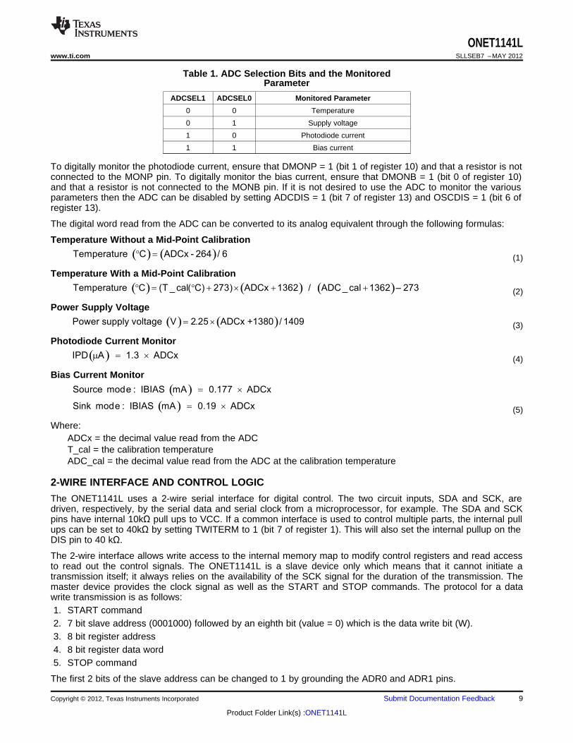
Table 1. ADC Selection Bits and the MonitoredParameter
ADCSEL1 ADCSEL0 Monitored Parameter
0 0 Temperature
0 1 Supply voltage
1 0 Photodiode current
1 1 Bias current
To digitally monitor the photodiode current, ensure that DMONP = 1 (bit 1 of register 10) and that a resistor is notconnected to the MONP pin. To digitally monitor the bias current, ensure that DMONB = 1 (bit 0 of register 10)and that a resistor is not connected to the MONB pin. If it is not desired to use the ADC to monitor the variousparameters then the ADC can be disabled by setting ADCDIS = 1 (bit 7 of register 13) and OSCDIS = 1 (bit 6 ofregister 13).
The digital word read from the ADC can be converted to its analog equivalent through the following formulas:
Temperature Without a Mid-Point Calibration
(1)
Temperature With a Mid-Point Calibration
(2)
Power Supply Voltage
(3)
Photodiode Current Monitor
(4)
Bias Current Monitor
(5)
Where:ADCx = the decimal value read from the ADCT_cal = the calibration temperatureADC_cal = the decimal value read from the ADC at the calibration temperature
2-WIRE INTERFACE AND CONTROL LOGIC
The ONET1141L uses a 2-wire serial interface for digital control. The two circuit inputs, SDA and SCK, aredriven, respectively, by the serial data and serial clock from a microprocessor, for example. The SDA and SCKpins have internal 10kΩ pull ups to VCC. If a common interface is used to control multiple parts, the internal pullups can be set to 40kΩ by setting TWITERM to 1 (bit 7 of register 1). This will also set the internal pullup on theDIS pin to 40 kΩ.
The 2-wire interface allows write access to the internal memory map to modify control registers and read accessto read out the control signals. The ONET1141L is a slave device only which means that it cannot initiate atransmission itself; it always relies on the availability of the SCK signal for the duration of the transmission. Themaster device provides the clock signal as well as the START and STOP commands. The protocol for a datawrite transmission is as follows:1. START command2. 7 bit slave address (0001000) followed by an eighth bit (value = 0) which is the data write bit (W).3. 8 bit register address4. 8 bit register data word5. STOP command
The first 2 bits of the slave address can be changed to 1 by grounding the ADR0 and ADR1 pins.
Copyright © 2012, Texas Instruments Incorporated Submit Documentation Feedback 9
Product Folder Link(s) :ONET1141L

tBUF
tHDSTA
tRtLOW
tHDDAT
tHIGH
tF
tSUDAT tSUSTA
tHDSTA
tSUSTO
P S SP
SDA
SCK
ONET1141LSLLSEB7 –MAY 2012 www.ti.com
Regarding timing, the ONET1141L is I2C compatible. The typical timing is shown in Figure 2 and complete datawrite and read transfers are shown in Figure 3. Parameters for Figure 2 are defined in Table 2.
Bus Idle: Both SDA and SCK lines remain HIGH
Start Data Transfer: A change in the state of the SDA line, from HIGH to LOW, while the SCK line is HIGH,defines a START condition (S). Each data transfer is initiated with a START condition.
Stop Data Transfer: A change in the state of the SDA line from LOW to HIGH while the SCK line is HIGHdefines a STOP condition (P). Each data transfer is terminated with a STOP condition; however, if the master stillwishes to communicate on the bus, it can generate a repeated START condition and address another slavewithout first generating a STOP condition.
Data Transfer: Only one data byte can be transferred between a START and a STOP condition. The receiveracknowledges the transfer of data.
Acknowledge: Each receiving device, when addressed, is obliged to generate an acknowledge bit. Thetransmitter releases the SDA line and a device that acknowledges must pull down the SDA line during theacknowledge clock pulse in such a way that the SDA line is stable LOW during the HIGH period of theacknowledge clock pulse. Setup and hold times must be taken into account. When a slave-receiver doesn’tacknowledge the slave address, the data line must be left HIGH by the slave. The master can then generate aSTOP condition to abort the transfer. If the slave-receiver does acknowledge the slave address but some timelater in the transfer cannot receive any more data bytes, the master must abort the transfer. This is indicated bythe slave generating the not acknowledge on the first byte to follow. The slave leaves the data line HIGH and themaster generates the STOP condition.
Figure 2. I2C Timing Diagram
Table 2. Timing Diagram Definitions
SYMBOL PARAMETER MIN MAX UNIT
fSCK SCK clock frequency 400 kHz
tBUF Bus free time between STOP and START conditions 1.3 μs
tHDSTA Hold time after repeated START condition. After this period, the first clock pulse is generated 0.6 μs
tLOW Low period of the SCK clock 1.3 μs
tHIGH High period of the SCK clock 0.6 μs
tSUSTA Setup time for a repeated START condition 0.6 μs
tHDDAT Data HOLD time 0 μs
tSUDAT Data setup time 100 ns
tR Rise time of both SDA and SCK signals 300 ns
tF Fall time of both SDA and SCK signals 300 ns
tSUSTO Setup time for STOP condition 0.6 μs
10 Submit Documentation Feedback Copyright © 2012, Texas Instruments Incorporated
Product Folder Link(s) :ONET1141L

S Slave Address Wr A Register Address A Data Byte A P
1 7 11 8 1 8 11
S Slave Address Wr A Register Address A Data Byte N P
1 7 11 8 1 8 11
Write Sequence
Read Sequence
S
1
Slave Address Rd A
7 11
Legend
S Start Condition
Wr Write Bit (bit value = 0)
Rd Read Bit (bit value = 1)
A Acknowledge
N Not Acknowledge
P Stop Condition
ONET1141Lwww.ti.com SLLSEB7 –MAY 2012
Figure 3. Programming Sequence
REGISTER MAPPING
The register mapping for register addresses 0 (0x00) through 15 (0x0F) are shown in Table 3 through Table 18.Table 19 describes the circuit functionality based on the register settings.
Table 3. Register 0 (0x00) Mapping – Control Settingsregister address 0 (0x00)
bit 7 bit 6 bit 5 bit 4 bit 3 bit 2 bit 1 bit 0
ENA PDRNG1 PDRNG0 OLENA FLTEN POL EQENA PDPOL
Table 4. Register 1 (0x01) Mapping – Control Settingsregister address 1 (0x01)
bit 7 bit 6 bit 5 bit 4 bit 3 bit 2 bit 1 bit 0
TWITERM HIEFCENA HIEQGENA HCENA OCDIS BIASPOL DISMODE LOGENA
Table 5. Register 2 (0x02) Mapping – Modulation Currentregister address 2 (0x02)
bit 7 bit 6 bit 5 bit 4 bit 3 bit 2 bit 1 bit 0
– – – – – – MODC1 MODC0
Table 6. Register 3 (0x03) Mapping – Modulation Currentregister address 3 (0x03)
bit 7 bit 6 bit 5 bit 4 bit 3 bit 2 bit 1 bit 0
MODC9 MODC8 MODC7 MODC6 MODC5 MODC4 MODC3 MODC2
Copyright © 2012, Texas Instruments Incorporated Submit Documentation Feedback 11
Product Folder Link(s) :ONET1141L

ONET1141LSLLSEB7 –MAY 2012 www.ti.com
Table 7. Register 4 (0x04) Mapping – Bias Currentregister address 4 (0x04)
bit 7 bit 6 bit 5 bit 4 bit 3 bit 2 bit 1 bit 0
– – – – – – BIASC1 BIASC0
Table 8. Register 5 (0x05) Mapping – Bias Currentregister address 5 (0x05)
bit 7 bit 6 bit 5 bit 4 bit 3 bit 2 bit 1 bit 0
BIASC9 BIASC8 BIASC7 BIASC6 BIASC5 BIASC4 BIASC3 BIASC2
Table 9. Register 6 (0x06) Mapping – Equalizer Adjustregister address 6 (0x06)
bit 7 bit 6 bit 5 bit 4 bit 3 bit 2 bit 1 bit 0
EQADJ7 EQADJ6 EQADJ5 EQADJ4 EQADJ3 EQADJ2 EQADJ1 EQADJ0
Table 10. Register 7 (0x07) Mapping – Cross Point Adjustregister address 7 (0x07)
bit 7 bit 6 bit 5 bit 4 bit 3 bit 2 bit 1 bit 0
CPSGN CPADJ6 CPADJ5 CPADJ4 CPADJ3 CPADJ2 CPADJ1 CPADJ0
Table 11. Register 8 (0x08) Mapping – Cross Point Control Settingsregister address 8 (0x08)
bit 7 bit 6 bit 5 bit 4 bit 3 bit 2 bit 1 bit 0
IDRV – – CPREF – CPENA CPRNG1 CPRNG0
Table 12. Register 9 (0x09) Mapping – Limiter Bias Current Adjustregister address 9 (0x09)
bit 7 bit 6 bit 5 bit 4 bit 3 bit 2 bit 1 bit 0
LIMCSGN LMC2 LIMC1 LIMC0 EFCSGN EFC2 EFC1 EFC0
Table 13. Register 10 (0x0A) Mapping – Monitor Settingsregister address 10 (0x0A)
bit 7 bit 6 bit 5 bit 4 bit 3 bit 2 bit 1 bit 0
– – – – – MONPFLT DMONP DMONB
Table 14. Register 11 (0x0B) Mapping – Bias Monitor Fault Settingsregister address 11 (0x0B)
bit 7 bit 6 bit 5 bit 4 bit 3 bit 2 bit 1 bit 0
BMF7 BMF6 BMF5 BMF4 BMF3 BMF2 BMF1 BMF0
Table 15. Register 12 (0x0C) Mapping – Power Monitor Fault Settingsregister address 12 (0x0C)
bit 7 bit 6 bit 5 bit 4 bit 3 bit 2 bit 1 bit 0
PMF7 PMF6 PMF5 PMF4 PMF3 PMF2 PMF1 PMF0
Table 16. Register 13 (0x0D) Mapping – ADC Settingsregister address 13 (0x0D)
bit 7 bit 6 bit 5 bit 4 bit 3 bit 2 bit 1 bit 0
ADCDIS OSCDIS – – – – ADCSEL1 ADCSEL0
12 Submit Documentation Feedback Copyright © 2012, Texas Instruments Incorporated
Product Folder Link(s) :ONET1141L

ONET1141Lwww.ti.com SLLSEB7 –MAY 2012
Table 17. Register 14 (0x0E) Mapping – ADC Output (Read Only)register address 14 (0x0E)
bit 7 bit 6 bit 5 bit 4 bit 3 bit 2 bit 1 bit 0
ADC9 ADC8 ADC7 ADC6 ADC5 ADC4 ADC3 ADC2
Table 18. Register 15 (0x0F) Mapping – ADC Output (Read Only)register address 15 (0x0F)
bit 7 bit 6 bit 5 bit 4 bit 3 bit 2 bit 1 bit 0
– – – – – – ADC1 ADC0
Table 19. Register Functionality
REGISTER BIT SYMBOL FUNCTION
7 ENA Enable chip bit1 = Chip enabled. Can be toggled low to reset a fault condition.0 = Chip disabled
6 PDRNG1 Photodiode current range bits5 PDRNG0 1X: up to 3080µA / 3µA resolution
01: up to 1540µA / 1.5µA resolution00: up to 770μA / 0.75μA resolution
4 OLENA Open loop enable bit1 = Open loop bias current control,0 = Closed loop bias current control
3 FLTEN Fault detection enable bit0
1 = Fault detection on0 = Fault detection off
2 POL Output polarity switch bit1: pin 22 = OUT- and pin 21= OUT+0: pin 22 = OUT+ and pin 21 = OUT-
1 EQENA Equalizer enable bit1 = Equalizer is enabled0 = Equalizer is disabled and bypassed
0 PDPOL Photodiode polarity bit1 = Photodiode cathode connected to VCC0 = Photodiode anode connected to GND
Copyright © 2012, Texas Instruments Incorporated Submit Documentation Feedback 13
Product Folder Link(s) :ONET1141L

ONET1141LSLLSEB7 –MAY 2012 www.ti.com
Table 19. Register Functionality (continued)
REGISTER BIT SYMBOL FUNCTION
7 TWITERM Two wire interface input termination select bit1 = 40kΩ selected0 = 10kΩ selected
6 HIEFCENA High emitter follower drive current enable bit1 = High current enabled0 = High current disabled
5 HIEQGENA High gain enable for EQ stage (with EQENA = 1)1 = High gain enabled0 = High gain disabled
4 HCENA High modulation current enable bit1 = High modulation current enabled0 = High modulation current disabled
13 OCDIS Offset cancellation disable bit
1 = DC offset cancellation is disabled0 = DC offset cancellation is enabled
2 BIASPOL Bias current polarity bit1 = Bias pin sinks current0 = Bias pin sources current
1 DISMODE Disable mode setting bit1 = Only the output stage is disabled (fast disable mode)0 = Major parts of the signal path are disabled
0 LOGENA Low gain enable for input amplifier (with EQENA = 0)1 = Low gain enabled0 = Default gain
3 7 MODC9 Modulation current setting: sets the output voltage
6 MODC8
5 MODC7 Output Voltage: 2.3Vpp / 2.5mV steps
4 MODC6
3 MODC5
2 MODC4
1 MODC3
0 MODC2
2 1 MODC1
0 MODC0
5 7 BIASC9 Bias curent settingsClosed loop (APC):
6 BIASC8 Coupling ratio CR = IBIAS / IPD, BIASC = 0..1023, IBIAS ≤ 150mA:
5 BIASC7
4 BIASC6 PDRNG = 00 (see above); IBIAS = 0.75µA x CR x BIASC
3 BIASC5 PDRNG = 01 (see above); IBIAS = 1.5µA x CR x BIASC
2 BIASC4 PDRNG = 1X (see above); IBIAS = 3µA x CR x BIASC
1 BIASC3
0 BIASC2 Open loop:
1 BIASC1 IBIAS ~ 150µA x BIASC in source mode4
0 BIASC0 IBIAS ~ 100µA x BIASC in sink mode
14 Submit Documentation Feedback Copyright © 2012, Texas Instruments Incorporated
Product Folder Link(s) :ONET1141L

ONET1141Lwww.ti.com SLLSEB7 –MAY 2012
Table 19. Register Functionality (continued)
REGISTER BIT SYMBOL FUNCTION
7 EQADJ7 Equalizer adjustment setting
6 EQADJ6
5 EQADJ5 EQENA = 0 (see above)
4 EQADJ4 Equalizer is turned off and bypassed6
3 EQADJ3
2 EQADJ2 EQENA = 1 (see above)
1 EQADJ1 Maximum equalization for 00000000
0 EQADJ0 Minimum equalization for 11111111
7 7 CPSGN Eye cross-point adjustment setting
6 CPADJ6 CPSGN = 1 (positive shift)
5 CPADJ5 Maximum shift for 1111111
4 CPADJ4 Minimum shift for 0000000
3 CPADJ3 CPSGN = 0 (negative shift)
2 CPADJ2 Maximum shift for 1111111
1 CPADJ1 Minimum shift for 0000000
0 CPADJ0
8 7 IDRV Output Driver Tail Current Bit1 = Output driver tail current is increased0 = Output driver tail current is set to default
6 -
5 -
4 CPREF Cross point temperature coefficient selection bit1 = Reverses the behaviorMM and EQENA = 1: temperature coefficient disabledMM and EQENA = 0: temperature coefficient enabled0 = Default conditionMM and EQENA = 1: temperature coefficient enabledMM and EQENA = 0: temperature coefficient disabled
3 -
2 CPENA Cross point adjustment enable bit1 = Cross point adjustment is enabled0 = Cross point adjustment is disabled
1 CPRNG1 Cross point adjustment range bits0 CPRNG0 Minimum adjustment range for 00
Maximum adjustment range for 11
9 7 LIMCSGN Limiter bias current sign bit1 = Decrease limiter bias current0 = Increase limiter bias current
6 LIMC2 Limiter bias current selection bits5 LIMC1 000 = No change4 LIMC0 111 = Maximum current change
3 EFCSGN Emitter follower sign bit1 = Decrease emitter follower current0 = Increase emitter follower current
2 EFC2 Emitter follower current selection bits1 EFC1 000 = No change0 EFC0 111 = Maximum current change
Copyright © 2012, Texas Instruments Incorporated Submit Documentation Feedback 15
Product Folder Link(s) :ONET1141L

ONET1141LSLLSEB7 –MAY 2012 www.ti.com
Table 19. Register Functionality (continued)
REGISTER BIT SYMBOL FUNCTION
10 7 -
6 -
5 -
4 -
3 -
2 MONPFLT Analog photodiode current monitor fault trigger bit1 = Fault trigger on MONP pin is enabled0 = Fault trigger on MONP pin is disabled
1 DMONP Digital photodiode current monitor selection bit (MONP)1 = Digital photodiode monitor is active (external resistor must not be installed)0 = Analog photodiode monitor is active (external resistor is required)
0 DMONB Digital bias current monitor selection bit (MONB)1 = Digital bias current monitor is active (external resistor must not be installed)0 = Analog bias current monitor is active (external resistor is required)
11 7 BMF7 Bias current monitor fault threshold
6 BMF6 With DMONB = 1
5 BMF5 Register sets the value of the bias current that will trigger a fault.
4 BMF4 The external resistor on the MONB pin must be removed to use this feature.
3 BMF3
2 BMF2
1 BMF1
0 BMF0
12 7 PMF7 Power monitor fault threshold
6 PMF6 With DMONP = 1
5 PMF5 Register sets the value of the photodiode current that will trigger a fault
4 PMF4 The external resistor on the MONP pin must be removed to use this feature.
3 PMF3
2 PMF2
1 PMF1
0 PMF0
13 7 ADCDIS ADC disable bit1 = ADC disabled0 = ADC enabled
6 OSCDIS ADC oscillator bit1 = Oscillator disabled0 = Oscillator enabled
5
4
3
2
1 ADCSEL1 ADC input selection bits0 ADCSEL0 00 selects the temperature sensor
01 selects the power supply monitor10 selects MONP11 selects MONB
16 Submit Documentation Feedback Copyright © 2012, Texas Instruments Incorporated
Product Folder Link(s) :ONET1141L

ONET1141Lwww.ti.com SLLSEB7 –MAY 2012
Table 19. Register Functionality (continued)
REGISTER BIT SYMBOL FUNCTION
14 7 ADC9 (MSB) Digital representation of the ADC input source (read only)
6 ADC8
5 ADC7
4 ADC6
3 ADC5
2 ADC4
1 ADC3
0 ADC2
15 7 -
6 -
5 -
4 -
3 -
2 -
1 ADC1 Digital representation of the ADC input source (read only)
0 ADC0 (LSB)
LASER SAFETY FEATURES AND FAULT RECOVERY PROCEDURE
The ONET1141L provides built in laser safety features. The following fault conditions are detected:1. Voltage at MONB exceeds the voltage at RZTC (1.16V) or, alternately, if DMONB = 1 and the bias current
exceeds the bias current monitor fault threshold set by BMF[0..7] (register 11). When using the digitalmonitor, the resistor to ground must be removed.
2. Voltage at MONP exceeds the voltage at RZTC (1.16V) and the analog photodiode current monitor faulttrigger bit, MONPFLT (bit 2 of register 10), is set to 1. Alternately, a fault can be triggered if DMONP = 1 andthe photodiode current exceeds the photodiode current monitor fault threshold set by PMF[0..7] (register 12).When using the digital monitor, the resistor to ground must be removed.
3. Photodiode current exceeds 150% of its set value,4. Bias control DAC drops in value by more than 50% in one step.
If one or more fault conditions occur and the fault enable bit FLTEN is set to 1, the ONET1141L responds by:1. Setting the bias current to zero.2. Setting the modulation current to zero.3. Asserting and latching the FLT pin.
Fault recovery is performed by the following procedure:1. The disable pin DIS and/or the internal enable control bit ENA are toggled for at least the fault latch reset
time.2. The FLT pin de-asserts while the disable pin DIS is asserted or the enable bit ENA is de-asserted.3. If the fault condition is no longer present, the part will return to normal operation with its prior output settings
after the disable negate time.4. If the fault condition is still present, FLT re-asserts once DIS is set to a low level and the part will not return to
normal operation.
Copyright © 2012, Texas Instruments Incorporated Submit Documentation Feedback 17
Product Folder Link(s) :ONET1141L

Dete
rmin
isti
c J
itte
r -
ps
pp
0
2
4
6
8
-40 -20 0 20 40 60 80 100
T - Free-Air Temperature - °CA
0
2
4
6
8
10
12
De
term
inis
tic
Jit
ter
- p
sp
p
300 400 500 600 700 800 900 1000
Modulation Current Register Setting - Decimal
-40 -20 0 20 40 60 80 100
T - Free-Air Temperature - °CA
0
0.1
0.2
0.3
0.4
Ra
nd
om
Jit
ter
- p
srm
s
0
0.1
0.2
0.3
0.4
0.5
0.6
0.7
0.8
0.9
1
Ra
nd
om
Jit
ter
- p
srm
s
300 400 500 600 700 800 900 1000
Modulation Current Register Setting - Decimal
ONET1141LSLLSEB7 –MAY 2012 www.ti.com
TYPICAL CHARACTERISTICSTypical operating condition is at VCC = 3.3V, TA = 25°C, IBIASC = 80mA, VOUT = 2VPP, VIN = 400mVpp (unless otherwise noted).
DETERMINISTIC JITTER DETERMINISTIC JITTERvs vs
MODULATION CURRENT TEMPERATURE
Figure 4. Figure 5.
RANDOM JITTER RANDOM JITTERvs vs
MODULATION CURRENT TEMPERATURE
Figure 6. Figure 7.
18 Submit Documentation Feedback Copyright © 2012, Texas Instruments Incorporated
Product Folder Link(s) :ONET1141L

0
5
10
15
20
25
30
35
Tra
nsit
ion
Tim
e -
ps
-40 -20 0 20 40 60 80 100
T - Free-Air Temperature - °CA
Rise Time
Fall Time
300 400 500 600 700 800 900 1000
Modulation Current Register Setting - Decimal
0
5
10
15
20
25
30
35
Tra
nsit
ion
Tim
e -
ps
Rise Time
Fall Time
400 600 800 1000
Bias Current Register Setting - Decimal
12002000
80
0
20
40
60
100
120
Sin
k O
LB
ias
Cu
rre
nt
- m
A
0
20
40
60
80
100
120
140
160
180
So
urc
e O
LB
ias C
urr
en
t -
mA
400 600 800 1000
Bias Current Register Setting - Decimal
12002000
ONET1141Lwww.ti.com SLLSEB7 –MAY 2012
TYPICAL CHARACTERISTICS (continued)Typical operating condition is at VCC = 3.3V, TA = 25°C, IBIASC = 80mA, VOUT = 2VPP, VIN = 400mVpp (unless otherwise noted).
RISE-TIME AND FALL-TIME RISE-TIME AND FALL-TIMEvs vs
MODULATION CURRENT TEMPERATURE
Figure 8. Figure 9.
BIAS CURRENT IN OPEN LOOP MODE BIAS CURRENT IN OPEN LOOP MODEvs vs
BIAS CURRENT REGISTER SETTING BIAS CURRENT REGISTER SETTING
Figure 10. Figure 11.
Copyright © 2012, Texas Instruments Incorporated Submit Documentation Feedback 19
Product Folder Link(s) :ONET1141L

0
0.2
0.4
0.6
0.8
1
1.2
1.4
1.6
1.8
Bia
s M
on
ito
r C
urren
t -
mA
0 20 40 60 80 100 120 140 160 180
Bias Current - mA
0
0.2
0.4
0.6
0.8
Ph
oto
dio
de M
on
ito
r C
urren
t -
mA
0 0.2 0.4 0.6 0.8 1 1.2 1.4 1.6
Photodiode Current - mA
Modulation Current Register Setting - Decimal
0
0.5
1
1.5
2
2.5
3
0 200 400 600 800 1000 1200
SE
Ou
tpu
t V
olt
ag
e -
V
-40 -20 0 20 40 60 80 100
T - Free-Air Temperature - °CA
100
110
120
130
140
150
160
170
180
190
200
Su
pp
ly C
urr
en
t -
mA
ONET1141LSLLSEB7 –MAY 2012 www.ti.com
TYPICAL CHARACTERISTICS (continued)Typical operating condition is at VCC = 3.3V, TA = 25°C, IBIASC = 80mA, VOUT = 2VPP, VIN = 400mVpp (unless otherwise noted).
PHOTODIODE MONITOR CURRENTBIAS MONITOR CURRENTvs vs
BIAS CURRENT PHOTODIODE CURRENT
Figure 12. Figure 13.
OUTPUT VOLTAGE SUPPLY CURRENTvs vs
MODC REGISTER SETTING TEMPERATURE
Figure 14. Figure 15.
20 Submit Documentation Feedback Copyright © 2012, Texas Instruments Incorporated
Product Folder Link(s) :ONET1141L

500 mV/div 15 ps/div 500 mV/div 15 ps/div
500 mV/div 15 ps/div 500 mV/div 15 ps/div
500 mV/div 15 ps/div
ONET1141Lwww.ti.com SLLSEB7 –MAY 2012
TYPICAL CHARACTERISTICS (continued)Typical operating condition is at VCC = 3.3V, TA = 25°C, IBIASC = 80mA, VOUT = 2VPP, VIN = 400mVpp (unless otherwise noted).
EYE-DIAGRAM AT 10.31GBPS EYE-DIAGRAM AT 11.3GBPSVOUT=2VPP, EQ Set to 00 VOUT=2VPP, EQ Set to 00, 50% Cross Point
Figure 16. Figure 17.
EYE-DIAGRAM AT 11.3GBPS EYE-DIAGRAM AT 11.3GBPSVOUT=2VPP, EQ Set to 00, 30% Cross Point VOUT=2VPP, EQ Set to 00, 70% Cross Point
Figure 18. Figure 19.
EYE-DIAGRAM AT 11.3GBPSVOUT=2VPP, EQ Set to 00,
6’’ OF FR4 AT INPUTS
Figure 20.
Copyright © 2012, Texas Instruments Incorporated Submit Documentation Feedback 21
Product Folder Link(s) :ONET1141L

MO
NP
DIN+
DIN–
MO
NB
MOD+
MOD-
VCCO
PD
AD
R0
DIS
SC
K
SD
A
GND
GND
GND
FLT
GND
RZTC
AD
R1
BIA
S
GN
D
VC
C
CO
MP
ONET1141LDIN+
DIN-
C1
C2
0.1μF
0.1μF
FLT
RZTC
RMONB
5kΩ
1kΩ
RMONP
MONB
MONP
SDA
SDK
DIS
0.1μF
Laser
0.1μF
VCC
0.1μF
0.1μF
0.1μF
0.1μF
0.01μF
CCOMP
50Ω
28.7kΩ
Modulator
Anode
EA BIAS
50Ω
PD
EML TOSA
0.01μF
VCCO
ONET1141LSLLSEB7 –MAY 2012 www.ti.com
APPLICATION INFORMATION
Figure 21 and Figure 22 show typical application circuits using the ONET1141L. The modulator must be ACcoupled to the driver for proper operation. The laser driver is controlled via the 2-wire interface SDA/SCK by amicrocontroller. In a typical application, the FLT, MONB and MONP outputs are also connected to themicrocontroller for transceiver management purposes.
The component values in Figure 21 and Figure 22 are typical examples and may be varied according to theintended application.
Figure 21. AC Coupled Drive with PD Monitor Cathode Available
22 Submit Documentation Feedback Copyright © 2012, Texas Instruments Incorporated
Product Folder Link(s) :ONET1141L

MO
NP
DIN+
DIN–
MO
NB
MOD+
MOD-
PD
AD
R0
DIS
SC
K
SD
A
GND
GND
FLT
GND
RZTCA
DR
1
BIA
S
GN
D
VC
C
CO
MP
ONET1141LDIN+
DIN-
C1
C2
0.1μF
0.1μF
FLT
RZTC
RMONB
5kΩ
1kΩ
RMONP
MONB
MONP
SDA
SDK
DIS
0.1μF
Laser
0.1μF
VCC
0.1μF
0.1μF
0.1μF
0.1μF
0.01μF
CCOMP
50Ω
28.7kΩ
Modulator
Anode
EA BIAS
50Ω
PD
EML TOSA
0.01μF
-3V
VCCO
VCCO
GND
ONET1141Lwww.ti.com SLLSEB7 –MAY 2012
Figure 22. AC Coupled Drive with PD Monitor Anode Available
Layout Guidelines
For optimum performance, use 50Ω transmission lines (100Ω differential) for connecting the signal source to theDIN+ and DIN– pins and 50Ω transmission lines (100Ω differential) for connecting the modulation currentoutputs, MOD+ and MOD–, to the laser. The length of the transmission lines should be kept as short as possibleto reduce loss and pattern-dependent jitter.
Copyright © 2012, Texas Instruments Incorporated Submit Documentation Feedback 23
Product Folder Link(s) :ONET1141L

PACKAGE OPTION ADDENDUM
www.ti.com 7-Jan-2015
Addendum-Page 1
PACKAGING INFORMATION
Orderable Device Status(1)
Package Type PackageDrawing
Pins PackageQty
Eco Plan(2)
Lead/Ball Finish(6)
MSL Peak Temp(3)
Op Temp (°C) Device Marking(4/5)
Samples
ONET1141LRGER ACTIVE VQFN RGE 24 3000 Green (RoHS& no Sb/Br)
CU NIPDAU Level-2-260C-1 YEAR -40 to 100 ONET1141L
ONET1141LRGET ACTIVE VQFN RGE 24 250 Green (RoHS& no Sb/Br)
CU NIPDAU Level-2-260C-1 YEAR -40 to 100 ONET1141L
(1) The marketing status values are defined as follows:ACTIVE: Product device recommended for new designs.LIFEBUY: TI has announced that the device will be discontinued, and a lifetime-buy period is in effect.NRND: Not recommended for new designs. Device is in production to support existing customers, but TI does not recommend using this part in a new design.PREVIEW: Device has been announced but is not in production. Samples may or may not be available.OBSOLETE: TI has discontinued the production of the device.
(2) Eco Plan - The planned eco-friendly classification: Pb-Free (RoHS), Pb-Free (RoHS Exempt), or Green (RoHS & no Sb/Br) - please check http://www.ti.com/productcontent for the latest availabilityinformation and additional product content details.TBD: The Pb-Free/Green conversion plan has not been defined.Pb-Free (RoHS): TI's terms "Lead-Free" or "Pb-Free" mean semiconductor products that are compatible with the current RoHS requirements for all 6 substances, including the requirement thatlead not exceed 0.1% by weight in homogeneous materials. Where designed to be soldered at high temperatures, TI Pb-Free products are suitable for use in specified lead-free processes.Pb-Free (RoHS Exempt): This component has a RoHS exemption for either 1) lead-based flip-chip solder bumps used between the die and package, or 2) lead-based die adhesive used betweenthe die and leadframe. The component is otherwise considered Pb-Free (RoHS compatible) as defined above.Green (RoHS & no Sb/Br): TI defines "Green" to mean Pb-Free (RoHS compatible), and free of Bromine (Br) and Antimony (Sb) based flame retardants (Br or Sb do not exceed 0.1% by weightin homogeneous material)
(3) MSL, Peak Temp. - The Moisture Sensitivity Level rating according to the JEDEC industry standard classifications, and peak solder temperature.
(4) There may be additional marking, which relates to the logo, the lot trace code information, or the environmental category on the device.
(5) Multiple Device Markings will be inside parentheses. Only one Device Marking contained in parentheses and separated by a "~" will appear on a device. If a line is indented then it is a continuationof the previous line and the two combined represent the entire Device Marking for that device.
(6) Lead/Ball Finish - Orderable Devices may have multiple material finish options. Finish options are separated by a vertical ruled line. Lead/Ball Finish values may wrap to two lines if the finishvalue exceeds the maximum column width.
Important Information and Disclaimer:The information provided on this page represents TI's knowledge and belief as of the date that it is provided. TI bases its knowledge and belief on informationprovided by third parties, and makes no representation or warranty as to the accuracy of such information. Efforts are underway to better integrate information from third parties. TI has taken andcontinues to take reasonable steps to provide representative and accurate information but may not have conducted destructive testing or chemical analysis on incoming materials and chemicals.TI and TI suppliers consider certain information to be proprietary, and thus CAS numbers and other limited information may not be available for release.

PACKAGE OPTION ADDENDUM
www.ti.com 7-Jan-2015
Addendum-Page 2
In no event shall TI's liability arising out of such information exceed the total purchase price of the TI part(s) at issue in this document sold by TI to Customer on an annual basis.

TAPE AND REEL INFORMATION
*All dimensions are nominal
Device PackageType
PackageDrawing
Pins SPQ ReelDiameter
(mm)
ReelWidth
W1 (mm)
A0(mm)
B0(mm)
K0(mm)
P1(mm)
W(mm)
Pin1Quadrant
ONET1141LRGER VQFN RGE 24 3000 330.0 12.4 4.3 4.3 1.5 8.0 12.0 Q2
ONET1141LRGET VQFN RGE 24 250 330.0 12.4 4.3 4.3 1.5 8.0 12.0 Q2
PACKAGE MATERIALS INFORMATION
www.ti.com 9-Aug-2017
Pack Materials-Page 1

*All dimensions are nominal
Device Package Type Package Drawing Pins SPQ Length (mm) Width (mm) Height (mm)
ONET1141LRGER VQFN RGE 24 3000 367.0 367.0 38.0
ONET1141LRGET VQFN RGE 24 250 367.0 367.0 38.0
PACKAGE MATERIALS INFORMATION
www.ti.com 9-Aug-2017
Pack Materials-Page 2

GENERIC PACKAGE VIEW
Images above are just a representation of the package family, actual package may vary.Refer to the product data sheet for package details.
RGE 24 VQFN - 1 mm max heightPLASTIC QUAD FLATPACK - NO LEAD
4204104/H

www.ti.com
PACKAGE OUTLINE
C
SEE TERMINALDETAIL
24X 0.30.2
2.45 0.1
24X 0.50.3
1 MAX
(0.2) TYP
0.050.00
20X 0.5
2X2.5
2X 2.5
A 4.13.9
B
4.13.9
0.30.2
0.50.3
VQFN - 1 mm max heightRGE0024BPLASTIC QUAD FLATPACK - NO LEAD
4219013/A 05/2017
PIN 1 INDEX AREA
0.08 C
SEATING PLANE
1
6 13
18
7 12
24 19
(OPTIONAL)PIN 1 ID
0.1 C A B0.05
EXPOSEDTHERMAL PAD
25 SYMM
SYMM
NOTES: 1. All linear dimensions are in millimeters. Any dimensions in parenthesis are for reference only. Dimensioning and tolerancing per ASME Y14.5M. 2. This drawing is subject to change without notice. 3. The package thermal pad must be soldered to the printed circuit board for thermal and mechanical performance.
SCALE 3.000
DETAILOPTIONAL TERMINAL
TYPICAL

www.ti.com
EXAMPLE BOARD LAYOUT
0.07 MINALL AROUND
0.07 MAXALL AROUND
24X (0.25)
24X (0.6)
( 0.2) TYPVIA
20X (0.5)
(3.8)
(3.8)
( 2.45)
(R0.05)TYP
(0.975) TYP
VQFN - 1 mm max heightRGE0024BPLASTIC QUAD FLATPACK - NO LEAD
4219013/A 05/2017
SYMM
1
6
7 12
13
18
1924
SYMM
LAND PATTERN EXAMPLEEXPOSED METAL SHOWN
SCALE:15X
NOTES: (continued) 4. This package is designed to be soldered to a thermal pad on the board. For more information, see Texas Instruments literature number SLUA271 (www.ti.com/lit/slua271).5. Vias are optional depending on application, refer to device data sheet. If any vias are implemented, refer to their locations shown on this view. It is recommended that vias under paste be filled, plugged or tented.
25
SOLDER MASKOPENING
METAL UNDERSOLDER MASK
SOLDER MASKDEFINED
EXPOSEDMETAL
METAL
SOLDER MASKOPENING
SOLDER MASK DETAILS
NON SOLDER MASKDEFINED
(PREFERRED)
EXPOSEDMETAL

www.ti.com
EXAMPLE STENCIL DESIGN
24X (0.6)
24X (0.25)
20X (0.5)
(3.8)
(3.8)
4X ( 1.08)
(0.64)TYP
(0.64) TYP
(R0.05) TYP
VQFN - 1 mm max heightRGE0024BPLASTIC QUAD FLATPACK - NO LEAD
4219013/A 05/2017
NOTES: (continued) 6. Laser cutting apertures with trapezoidal walls and rounded corners may offer better paste release. IPC-7525 may have alternate design recommendations.
25
SYMM
METALTYP
SOLDER PASTE EXAMPLEBASED ON 0.125 mm THICK STENCIL
EXPOSED PAD 25
78% PRINTED SOLDER COVERAGE BY AREA UNDER PACKAGESCALE:20X
SYMM
1
6
7 12
13
18
1924

IMPORTANT NOTICE
Texas Instruments Incorporated (TI) reserves the right to make corrections, enhancements, improvements and other changes to itssemiconductor products and services per JESD46, latest issue, and to discontinue any product or service per JESD48, latest issue. Buyersshould obtain the latest relevant information before placing orders and should verify that such information is current and complete.TI’s published terms of sale for semiconductor products (http://www.ti.com/sc/docs/stdterms.htm) apply to the sale of packaged integratedcircuit products that TI has qualified and released to market. Additional terms may apply to the use or sale of other types of TI products andservices.Reproduction of significant portions of TI information in TI data sheets is permissible only if reproduction is without alteration and isaccompanied by all associated warranties, conditions, limitations, and notices. TI is not responsible or liable for such reproduceddocumentation. Information of third parties may be subject to additional restrictions. Resale of TI products or services with statementsdifferent from or beyond the parameters stated by TI for that product or service voids all express and any implied warranties for theassociated TI product or service and is an unfair and deceptive business practice. TI is not responsible or liable for any such statements.Buyers and others who are developing systems that incorporate TI products (collectively, “Designers”) understand and agree that Designersremain responsible for using their independent analysis, evaluation and judgment in designing their applications and that Designers havefull and exclusive responsibility to assure the safety of Designers' applications and compliance of their applications (and of all TI productsused in or for Designers’ applications) with all applicable regulations, laws and other applicable requirements. Designer represents that, withrespect to their applications, Designer has all the necessary expertise to create and implement safeguards that (1) anticipate dangerousconsequences of failures, (2) monitor failures and their consequences, and (3) lessen the likelihood of failures that might cause harm andtake appropriate actions. Designer agrees that prior to using or distributing any applications that include TI products, Designer willthoroughly test such applications and the functionality of such TI products as used in such applications.TI’s provision of technical, application or other design advice, quality characterization, reliability data or other services or information,including, but not limited to, reference designs and materials relating to evaluation modules, (collectively, “TI Resources”) are intended toassist designers who are developing applications that incorporate TI products; by downloading, accessing or using TI Resources in anyway, Designer (individually or, if Designer is acting on behalf of a company, Designer’s company) agrees to use any particular TI Resourcesolely for this purpose and subject to the terms of this Notice.TI’s provision of TI Resources does not expand or otherwise alter TI’s applicable published warranties or warranty disclaimers for TIproducts, and no additional obligations or liabilities arise from TI providing such TI Resources. TI reserves the right to make corrections,enhancements, improvements and other changes to its TI Resources. TI has not conducted any testing other than that specificallydescribed in the published documentation for a particular TI Resource.Designer is authorized to use, copy and modify any individual TI Resource only in connection with the development of applications thatinclude the TI product(s) identified in such TI Resource. NO OTHER LICENSE, EXPRESS OR IMPLIED, BY ESTOPPEL OR OTHERWISETO ANY OTHER TI INTELLECTUAL PROPERTY RIGHT, AND NO LICENSE TO ANY TECHNOLOGY OR INTELLECTUAL PROPERTYRIGHT OF TI OR ANY THIRD PARTY IS GRANTED HEREIN, including but not limited to any patent right, copyright, mask work right, orother intellectual property right relating to any combination, machine, or process in which TI products or services are used. Informationregarding or referencing third-party products or services does not constitute a license to use such products or services, or a warranty orendorsement thereof. Use of TI Resources may require a license from a third party under the patents or other intellectual property of thethird party, or a license from TI under the patents or other intellectual property of TI.TI RESOURCES ARE PROVIDED “AS IS” AND WITH ALL FAULTS. TI DISCLAIMS ALL OTHER WARRANTIES ORREPRESENTATIONS, EXPRESS OR IMPLIED, REGARDING RESOURCES OR USE THEREOF, INCLUDING BUT NOT LIMITED TOACCURACY OR COMPLETENESS, TITLE, ANY EPIDEMIC FAILURE WARRANTY AND ANY IMPLIED WARRANTIES OFMERCHANTABILITY, FITNESS FOR A PARTICULAR PURPOSE, AND NON-INFRINGEMENT OF ANY THIRD PARTY INTELLECTUALPROPERTY RIGHTS. TI SHALL NOT BE LIABLE FOR AND SHALL NOT DEFEND OR INDEMNIFY DESIGNER AGAINST ANY CLAIM,INCLUDING BUT NOT LIMITED TO ANY INFRINGEMENT CLAIM THAT RELATES TO OR IS BASED ON ANY COMBINATION OFPRODUCTS EVEN IF DESCRIBED IN TI RESOURCES OR OTHERWISE. IN NO EVENT SHALL TI BE LIABLE FOR ANY ACTUAL,DIRECT, SPECIAL, COLLATERAL, INDIRECT, PUNITIVE, INCIDENTAL, CONSEQUENTIAL OR EXEMPLARY DAMAGES INCONNECTION WITH OR ARISING OUT OF TI RESOURCES OR USE THEREOF, AND REGARDLESS OF WHETHER TI HAS BEENADVISED OF THE POSSIBILITY OF SUCH DAMAGES.Unless TI has explicitly designated an individual product as meeting the requirements of a particular industry standard (e.g., ISO/TS 16949and ISO 26262), TI is not responsible for any failure to meet such industry standard requirements.Where TI specifically promotes products as facilitating functional safety or as compliant with industry functional safety standards, suchproducts are intended to help enable customers to design and create their own applications that meet applicable functional safety standardsand requirements. Using products in an application does not by itself establish any safety features in the application. Designers mustensure compliance with safety-related requirements and standards applicable to their applications. Designer may not use any TI products inlife-critical medical equipment unless authorized officers of the parties have executed a special contract specifically governing such use.Life-critical medical equipment is medical equipment where failure of such equipment would cause serious bodily injury or death (e.g., lifesupport, pacemakers, defibrillators, heart pumps, neurostimulators, and implantables). Such equipment includes, without limitation, allmedical devices identified by the U.S. Food and Drug Administration as Class III devices and equivalent classifications outside the U.S.TI may expressly designate certain products as completing a particular qualification (e.g., Q100, Military Grade, or Enhanced Product).Designers agree that it has the necessary expertise to select the product with the appropriate qualification designation for their applicationsand that proper product selection is at Designers’ own risk. Designers are solely responsible for compliance with all legal and regulatoryrequirements in connection with such selection.Designer will fully indemnify TI and its representatives against any damages, costs, losses, and/or liabilities arising out of Designer’s non-compliance with the terms and provisions of this Notice.
Mailing Address: Texas Instruments, Post Office Box 655303, Dallas, Texas 75265Copyright © 2018, Texas Instruments Incorporated