slide 1-1 sequential logic the combinational logic circuits we have been studying have no memory....
TRANSCRIPT

Slide 1-1Sequential Logic• The combinational logic circuits we have been studying have no
memory. The outputs always follow the inputs.
• There is a need for circuits with a memory, which behave differently depending upon their previous state.
• An example is the vending machine, which must remember how many and what kinds of coins have been inserted, and which behave according to not only the current coin inserted, but also upon how many and what kind of coins have been deposited previously.
• These are referred to as finite state machines, because they can have at most a finite number of states.

Slide 1-2
Digital Techniques Fall 2007 André Deutz, Leiden University
(Synchronous) Finite State Machine (FSM):
clu
State elem
Theory
FSM

Slide 1-3
Digital Techniques Fall 2007 André Deutz, Leiden University
Finite State Machine (FSM)
• A finite state machine is s digital device having:– A finite set of States: S1, S2, …, Sk (where k is the number of
states, optionally one of this is distinguished as the initial state)– A finite number of binary Inputs I1, …, Im (where m is the number
of inputs)– A finite number of binary Outputs O1, …, On (where n is the
number of outputs)– A set of State Transition Rules rules, specifying for each choice of
current state Ss and input values I1, …, Im a next state Ss’ and – A set of output rules specifying for each choice of the current Ss
and input values I1, …, Im the binary value at each output

Slide 1-4
Digital Techniques Fall 2007 André Deutz, Leiden University
Finite State Machine (FSM)
• In a Moore machine the FSM’s outputs are functions of the current state alone
• The behavior of such a system can be specified by giving rules for making transitions between states and the set of output values corresponding to each state
• The alternative model, called a Mealy machine, allows outputs to reflect current inputs as well as current state.
• Most abstract representation of FSMs is a state-transition diagram

Slide 1-5
Digital Techniques Fall 2007 André Deutz, Leiden University
m nCombinational
Circuit StorageElementsNext
state Present state
k
feed-back loop
k
outputsinputs
(Synchronous) Finite State Machines
Clock- Acyclic graph- static discipline- Can exhaustively be enumerated by 2k+m rowsAnd k+n columns - Engineered cycles
- Works only if dynamic discipline obeyed- Remembers k bits for a total of 2k unique combinations combinations

Slide 1-6
Finite State Machine, in short:
Inp . . .
. . .
io
ik
Synchronizationsignal
fo
State bits
fmCombinationallogic unit
Qn
sn
Delay elements (one per state bit)
uts Outputs
Dn
Q0
s0
D0
. . .
. . .
. . . An FSM is
composed of a combinational logic unit and delay elements (called flip-flops) in a feedback path, which maintains state information.

Slide 1-7
Digital Techniques Fall 2007 André Deutz, Leiden University
The state of a sequential circuit is a collection of state variables whose values at any one time contain all the information about the past necessary to account for the circuit’s future behavior
Herbert Hellerman, Digital Computer Systems Principles,McGraw Hill, 1967, p237

Slide 1-8Finite State Machine Design• Counter has a clock input, CLK, and a RESET input.
• Has two output lines, which must take values of 00, 01, 10, and 11 on subsequent clock cycles.
It requires two flip-flops to store the state.
A Modulo-4 Counter
0 1 1 0 0
4 3 2 1 0 Time (t)
0 0 0 0 1
Time (t) 4 3 2 1 0
0 1 0 1 03-bitsynchronous
counter
CLK
D
s1
Q
Q
D
s0
Q
Q
q0
q1
s0
s1
RESET
2-bit

Slide 1-9
Digital Techniques Fall 2007 André Deutz, Leiden University
State Transition Diagram for Mod-4 Counter

Slide 1-10State Transition Diagram for a Modulo-4 Counter
• The state diagram and state table tell “all there is to know” about the FSM, and are the basis for a provably correct design.
Next State
Present State RESET 0 1
A B/01 A/00B C/10 A/00C D/11 A/00D A/00 A/00
StateTable
Present State RESET0 1
A:00 01 00B:01 10 00C:10 11 00D:11 00 00
StateTableWithStatesAssigned
Output 00state
Output 01state
Output 10state
Output 11state
BA
DC
01/1
1/00
q1
RESET0/01
1/00
0/11
0/10 0/001/00
1/00
q010/1

Slide 1-11
Digital Techniques Fall 2007 André Deutz, Leiden University
Arcs leaving a state must be:(1) mutually exclusive
– can’t have two choices for a given input value(2) collectively exhaustive
– every state must specify what happens for each possible input combination. “Nothing happens”means arc back to itself.
Valid State Transition Diagrams

Slide 1-12
Truth Table
• Develop equations from this truth table for s0(t+1), s1(t+1),q0(t+1), and q1(t+1) from inputs r(t), s0(t) and s1(t)
r(t) s1(t)s0(t) s1s0(t+1) q1q0(t+1)
0 00 01 01
0 01 10 10
0 10 11 11
0 11 00 00
1 00 00 00
1 01 00 00
1 10 00 00
1 11 00 00

Slide 1-13
Equations
s0(t 1) r(t)s1(t)s0(t) r(t)s1(t)s0(t)
s1(t 1) r(t)s1(t)s0(t ) r(t)s1(t)s0(t)
q0(t 1) r(t)s1(t)s0(t) r(t)s1(t)s0(t)
q1(t 1) r(t)s1(t)s0(t ) r(t)s1(t)s0(t)
Implement these equations

Slide 1-14Logic Design for a Modulo(4) Counter
There are many simpler techniques for implementing counters.
CLK
RESET
q1
q0
D
s1
Q
Q
D
s0
Q
Q
Slide 1-15
Digital Techniques Fall 2007 André Deutz, Leiden University
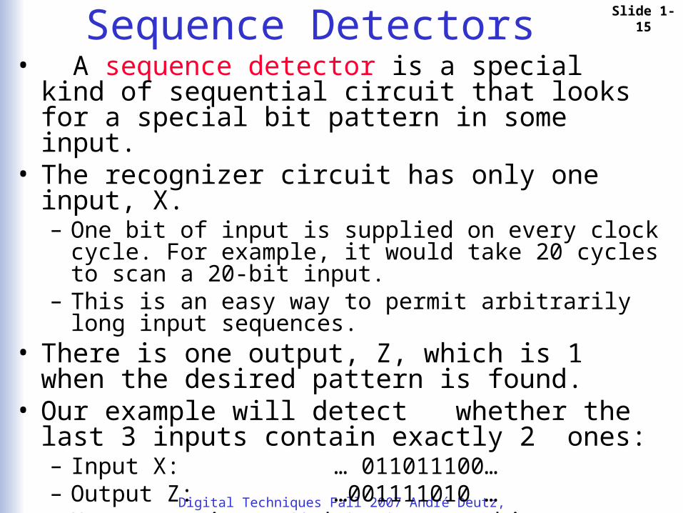
Sequence Detectors• A sequence detector is a special kind of sequential
circuit that looks for a special bit pattern in some input.• The recognizer circuit has only one input, X.
– One bit of input is supplied on every clock cycle. For example, it would take 20 cycles to scan a 20-bit input.
– This is an easy way to permit arbitrarily long input sequences.• There is one output, Z, which is 1 when the desired
pattern is found.• Our example will detect whether the last 3 inputs
contain exactly 2 ones:– Input X: … 011011100… – Output Z: …001111010 … – Here, one input and one output bit appear every clock cycle.
• This requires a sequential circuit because the circuit has to “remember” the inputs from previous clock cycles, in order to determine whether or not a match was found.

Slide 1-16
A Sequence Detector
• Design a machine that outputs a 1 when exactly 2 of the last 3 inputs are 1.
• e.g. input sequence of 011011100 produces an output sequence of 001111010
• Assume input is a 1-bit serial line.
• Use D flip-flops and 8-1 multiplexers.
• Begin by constructing a state transition diagram.

Slide 1-17
Digital Techniques Fall 2007 André Deutz, Leiden University
Sequence Detector State Transition Diagram
• Design a machine that outputs a 1 when exactly two of the last three inputs are 1.

Slide 1-18
Digital Techniques Fall 2007 André Deutz, Leiden University
Sequence Detector State Transition Diagram
• Design a machine that outputs a 1 when exactly two of the last three inputs are 1.
Take
s car
e of
firs
t or
of fi
rst t
wo
inpu
ts; s
ome-
Tim
es y
ou h
ave
no m
ore
Than
2 in
puts

Slide 1-19State Transition Diagram for Sequence Detector
• Design a machine that outputs a 1 when exactly 2 of the last 3 inputs are 1.
• Discuss: the “meaning” of each state.
Pres. XState 0 1S2S1S0 S2S1S0Z S2S1S0Z
A=000 001/0 010/0B=001 011/0 100/0C=010 101/0 110/0D=011 011/0 100/0E=100 101/0 110/1F=101 011/0 100/1G=110 101/1 110/0
• Convert table to truth table (how?).
• Solve for s2 s1 s0 and Z.
B
C
A
D
E
F
G
0/0
1/00/0
1/0
1/0
0/0
1/1
1/1
0/0
1/0
0/1
1/0
0/0
0/0

Slide 1-20
Sequence Detector State Table

Slide 1-21
Sequence Detector State Assignment

Slide 1-22
Logic Diagram for Sequence Detector
D
s2
Q
CLK
Q
D
s1
Q
Q
D
s0
Q Z
Q
000
001
010
011
100
101
110
111
0
x
1
x
1
x
1
0
000
001
010
011
100
101
110
111
x
x
x
x
x
x
x
0
000
001
010
011
100
101
110
111
x
x
x
x
x
x
x
0
000
001
010
011
100
101
110
111
0
0
0
0
x
x
x
0

Slide 1-23
A Vending Machine Controller
• Accepts nickel, dime, and quarter. When value of money inserted equals or exceeds twenty cents, machine vends item and returns change if any, and waits for next transaction.
• Implement with PLA and D flip-flops.
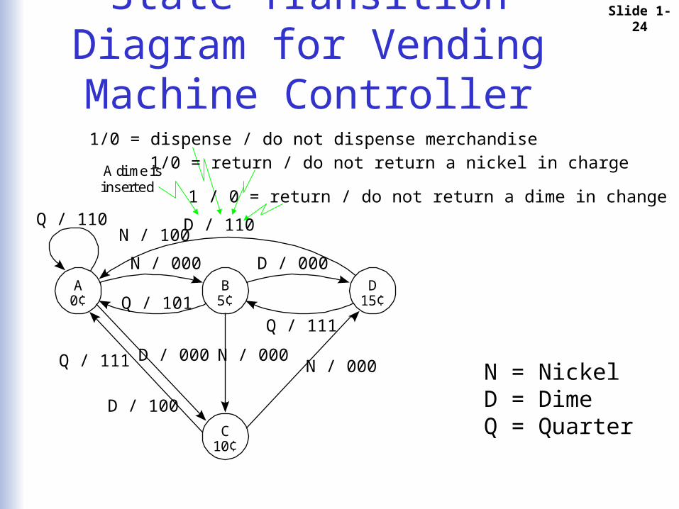
Slide 1-24State Transition Diagram for Vending Machine Controller
A0¢
B
A dime isinserted
5¢
C10¢
D15¢
N = NickelD = DimeQ = Quarter
N / 000
1/0 = dispense / do not dispense merchandise
1/0 = return / do not return a nickel in charge
Q / 111
D / 000
N / 100
N / 000
Q / 101
Q / 111
D / 100
D / 000 N / 000
Q / 110 D / 110
1 / 0 = return / do not return a dime in change

Slide 1-25Truth Table for Vending Machine Controller
0 0 0 0 0 0 1 0 0 01 0 0 0 1 1 0 0 0 02 0 0 1 0 0 0 1 1 03 0 0 1 1 d d d d d4 0 1 0 0 1 0 0 0 05 0 1 0 1 1 1 0 0 06 0 1 1 0 0 0 1 0 17 0 1 1 1 d d d d d8 1 0 0 0 1 1 0 0 09 1 0 0 1 0 0 1 0 0
1 0 1 0 1 0 0 0 1 1 11 1 1 0 1 1 d d d d d1 2 1 1 0 0 0 0 1 0 01 3 1 1 0 1 0 0 1 1 01 4 1 1 1 0 0 1 1 1 11 5 1 1 1 1 d d d d d
B a s e 1 0e q u iv a l e n t
P r e s e n ts t a t e C o i n
N e x ts t a t e
D i s p e n s e
R e t u r n n i c k e lR e t u r n d i m e
s1
s0
x1
x0
s1
s0
z2
z1
z0

Slide 1-26(a)FSM Circuit, (b)Truth Table, and (c)PLA Realization for Vending Machine Controller
s1x
0
x1
0 0 0 0 0 0 1 0 0 01 0 0 0 1 1 0 0 0 02 0 0 1 0 0 0 1 1 03 0 0 1 1 d d d d d4 0 1 0 0 1 0 0 0 05 0 1 0 1 1 1 0 0 06 0 1 1 0 0 0 1 0 17 0 1 1 1 d d d d d8 1 0 0 0 1 1 0 0 09 1 0 0 1 0 0 1 0 0
10 1 0 1 0 0 0 1 1 111 1 0 1 1 d d d d d12 1 1 0 0 0 0 1 0 013 1 1 0 1 0 0 1 1 014 1 1 1 0 0 1 1 1 115 1 1 1 1 d d d d d
z1z
0
z2
s0 x1 x0
s1 s0 z2 z1 z0
D
CLK
s0
Q
D
Base 10equivalent
Presentstate Coin
Nextstate
Dispense
Return nickelReturn dime
s1
s1
s0
x1
x0
s1
s0
z2
z1
z0
Q
0
1
2
4
5
6
8
9
10
12
13
14
(c)(b)
(a)
5 x 5PLA

Slide 1-27Moore Counter• Mealy Model: Outputs are functions of Inputs and Present State.
• Previous FSM designs were Mealy Machines, in which next state was computed from present state and inputs.
• Moore Model: Outputs are functions of Present State only.

Slide 1-28Mealy versus Moore Machines• Mealy model: Outputs are
functions of inputs and present state.
• Previous FSM designs were Mealy machines, because next state was computed from present state and inputs.
• Moore model: Outputs are functions of present state only.
• Both are equally powerful.CLK
D z0
z1
s0
Q1
0
x
Q
Ds1
00
01
10
11
4-to-1MUX
00
01
10
11
4-to-1MUX
Q
Q
x0
x1z1z0
2
D
CLK
s0
Q
Ds1
Q
5 x 5PLA
z

Slide 1-29
Digital Techniques Fall 2007 André Deutz, Leiden University
Step 1: Given the problem statement, derive the state (transition) table:The table should show inputs, present states, next states and outputs.It may be easier to find a state diagram first, and then convert that to a table.
Step 2 (optional): Apply state-reduction methods to reduce (if possible) the number of states.
We will not discuss state-reduction methods in this course.Step 3: Assign binary codes to the states in the state table, if you haven’t already.
If you have n states, your binary codes will have at least log2 n bits.Step 4: Determine the number of Flip-Flops needed and the type of Flip-Flops to be used:
If you have n states, your circuit will have at least log2 n Flip-Flops.The types of Flip-Flops may be given in the initial specification. If not, select the type according to some criteria, e.g., to get simpler circuit or to make the design procedure easier.
Summary of Design Procedure FSMs

Slide 1-30
Digital Techniques Fall 2007 André Deutz, Leiden University
Summary of Design Procedure FSMs
Step 5: For each flip-flop and each row of your state table, find the flip-flop input values that are needed to generate the next state from the present state:
You can use Flip-Flop excitation tables here.Step 6: Derive the characteristic (Flip-Flop input) equations from the state table. Step 7: Derive the primary output equations from the state table.Step 8: Simplify the Flip-Flop input equations and output equations:
Use K-maps or Other simplification methods
Step 9: Draw the logic diagram of the circuit.

Slide 1-31
FSMs
• They are here to stay • discussion
Digital Techniques Fall 2007 André Deutz, Leiden University

Slide 1-32
Digital Techniques Fall 2007 André Deutz, Leiden University
A
1/110/11
0/00 1/01
A /11
10
0 100 is accommodatedby next state 01 is
accommodatedby next state
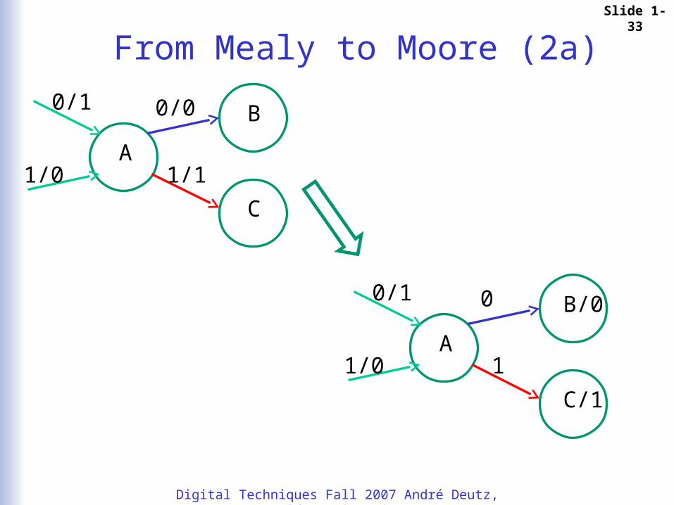
From Mealy to Moore (1)
Move output forward into the nextState. If this results in a state with two different outputs, then split that state intoas many states as there are different outputs. The next statesFrom the created states are the same as the original ones
Slide 1-33
Digital Techniques Fall 2007 André Deutz, Leiden University
A
0/0
From Mealy to Moore (2a)
B
C
1/1
0/1
1/0
A
0 B/0
C/1
1
0/1
1/0

Slide 1-34
Digital Techniques Fall 2007 André Deutz, Leiden University
From Mealy to Moore (2b)
A
0 B/0
C/1
1
0/1
1/0
A 0 B/0
C/1
1
0/1
1/0A
Split state to accommodatedifferent outputs.Destination from split states stays the same:

Slide 1-35
Digital Techniques Fall 2007 André Deutz, Leiden University
From Mealy to Moore (2c)A 0 B/0
C/1
1
0/1
1/0A
A1/1
0B/0
C/1
10
1A2/0
01

Slide 1-36
Change of Topics: back to Assembly

Slide 1-37
Pre-processor
(cpp)
hello.i Compiler(cc1)
hello.s Assembler(as)
hello.o Linker(ld)
hellohello.c
Sourceprogram(text)
Modifiedsourceprogram(text)
Assemblyprogram(text)
Relocatableobject
programs(binary)
Executableobjectprogram(binary)
printf.o
Programs are translated by other programs into differentforms
What happens when you enter:gcc –o hello hello.c?

Slide 1-38Remarks on Assembly Programming
• We will consider the Assembly Language of Tiny Mips
• The next slide summarizes the instruction set of TM; the slt, brlt and halt instructions will be considered as part of the repertoire as well
• Remember as powerful as C++ (obviously not as expressive as C++)
Digital Techniques Fall 2007 André Deutz, Leiden University

Slide 1-39
Digital Techniques Fall 2007 André Deutz, Leiden University

Slide 1-40
C++ to Assembly
• How would you translate the following fragments of C++ into TM Assembly:
int a, b;
a = 4;
b= 4;
a = a – b;
Digital Techniques Fall 2007 André Deutz, Leiden University

Slide 1-41
C++ to TM Assembly: selection
Digital Techniques Fall 2007 André Deutz, Leiden University
1) if (a < = b) {// true task (TT)} else {// false task (FT)}11
2) Assume a and b are fetched from memory andStored in reg0 and reg1 respectivelySet negation of condition (a < = b)(i.e.: test (b < a))brlt address of beginning of ft true taskbr address of instruction after if-then-else false task
3)slt reg1, reg0brlt “false task”
true taskbr “end of if-then-else” false task

Slide 1-42
C++ to TM Assembly: selection
Digital Techniques Fall 2007 André Deutz, Leiden University
1) if (a < b) {// true task (TT)} else {// false task (FT)}11
2) pseudo ?
3) assembly: ?
Slide 1-43
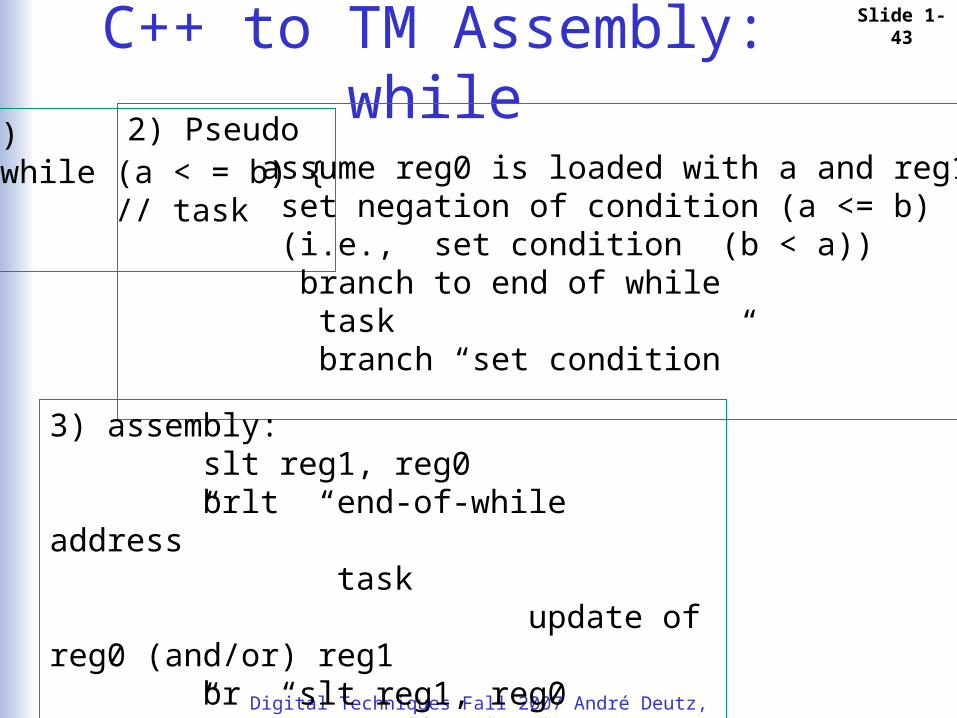
C++ to TM Assembly: while
Digital Techniques Fall 2007 André Deutz, Leiden University
1) while (a < = b) { // task}
2) Pseudo assume reg0 is loaded with a and reg1 with b set negation of condition (a <= b) (i.e., set condition (b < a)) branch to end of while
task branch “set condition”
3) assembly: slt reg1, reg0 brlt “end-of-while address” task update of reg0 (and/or) reg1 br “slt reg1, reg0 address”

Slide 1-44
Digital Techniques Fall 2007 André Deutz, Leiden University
a) write a TM assembly program which computes themaximum of two numbersb) write a TM assembly program which computes the maxof three numbersc) suppose the 0th memory location contains the numberof numbers (denoted by n). the next n memory locations contain n numbers. write a TM assembly program whichcomputes the max of these n numbers

Slide 1-45
Summary• Built an automatic information processing device (a la von Neumann)
– As primitives: AND, OR, NOT, state elements (d-latches and d-flip-flops); all these can be implemented on a macroscopic level – relays, waterpipes, knex)
– Combinational logic units (muxes, adders, ALUs)– Sequential circuits (most simple: d-latches and d-flip-flops; registers;
memory; ) – Von Neumann model; eternal von Neumann fetch-decode-execute cycle– Datapath– Control
• Other approaches: quantum computing, dna computing• Look also at the website of Great Principles of Computer Science
(http://cs.gmu.edu/cne/pjd/GP/ )

Slide 1-46
clock
data
Q (D-latch)
Time

Slide 1-47
clock
data
Q? D-latch
Time

Slide 1-48
clock
data
Q? D-latch
Time
D-flip-flopRising edgeQ?