slas343b – may 2001– revised april … instruments_ths8135.pdf · (itu-r.bt656)multiplexed...
TRANSCRIPT

THS8135
www.ti.com SLAS343B –MAY 2001–REVISED APRIL 2013
10-BIT 240-MSPS VIDEO DACWITH TRI-LEVEL SYNC AND VIDEO (ITU-R.BT601)-COMPLIANT FULL-SCALE RANGE
Check for Samples: THS8135
1FEATURES2• Triple 10-Bit D/A Converters • Bi-Level (EIA) or Tri-Level (SMPTE) Sync
Generation• 240-MSPS Operation• Integrated Sync-On-Green/Luminance or Sync-• YPbPr/RGB Configurable Blanking Levels,
On-All Composite Sync InsertionCorrectly Positioned for Either Full (0-1023) orVideo (ITU-R.BT601) Compliant Input Code • Internal Voltage ReferenceRanges • Low-Power Operation From 3.3-V Analog and
• Generic Triple DAC Mode for Non-Video 1.8-V Digital Suply LevelsApplications
APPLICATIONS• Direct Drive of Double-Terminated 75-Ω LoadInto Standard Video Levels • High-Definition Television (HDTV) Set-Top
Boxes/Receivers/Displays• 3x10 Bit 4:4:4, 2x10 Bit 4:2:2 or 1x10 Bit 4:2:2(ITU-R.BT656) Multiplexed YCbCr/GBR Input • High-Resolution Image ProcessingData Formats
DESCRIPTIONThe THS8135 is a general-purpose triple high-speed D/A converter optimized for use in video/graphicsapplications. The device operates from 3.3-V analog and 1.8-V digital supplies. The THS8135 performance isassured at a sampling rate up to 240 MSPS. The THS8135 consists of three 10-bit D/A converters and additionalcircuitry for bi-level/tri-level sync and blanking level generation. By providing a dc offset for the lowest videoamplitude output in video DAC mode, the device can insert a (negative) bi-level or (negative/positive) tri-levelsync on either only the green/luminance (sync-on-green/sync-on-Y) channel or on all channels for videoapplications. A generic DAC mode avoids this dc offset, making this device suitable for non-video applications aswell.
The THS8135 is a footprint-compatible functional upgrade to the THS8133. In addition, the THS8135 allows ahigher update rate for oversampled video digitizing for all PC graphics formats up to UXGA (1600x1200)resolution at 85 Hz and all practical digital TV formats including HDTV. The support for oversampling significantlyreduces the complexity of the analog reconstruction filter required behind the DAC.
Standard video levels can be generated for the full 10-bit input code range. Alternatively, the same levels can bereached from a reduced input code range compliant to the video sampling standard ITU-R.BT-601. In that case,the full-scale range of the DAC is dependent on the RGB or YCbCr color space configuration of the device.When configured for RGB operation, full video output swing is reached for input codes 64-940 on all channels.When configured for YCbCr operation, code range 64-940 on Y and code range 64-960 on Cb and Cr channelsgenerate full output swing using internal amplitude scaling on these color components. The device providesheadroom to accommodate under-/over-shoot outside the ITU-R.BT601 range to allow the generation of ITU-R.BT601 illegal colors or super-black / super-white levels.
A digital control input for insertion of a reference (blanking) level on the analog outputs is included. Theamplitude of the blanking level is configurable for either RGB or YPbPr component outputs and for full or reducedinput code ranges. The inserted sync output amplitude(s) always has the required 7:3 ratio to the full-scale videoamplitude.
The current-steering DACs can be directly terminated in resistive loads to produce voltage outputs. The deviceprovides a flexible configuration of maximum output current drive. The devices output drivers have beenspecifically designed to produce standard video output levels when directly connected to a single-ended double-terminated 75-Ω coaxial cable.1
Please be aware that an important notice concerning availability, standard warranty, and use in critical applications ofTexas Instruments semiconductor products and disclaimers thereto appears at the end of this data sheet.
2PowerPAD is a trademark of Texas Instruments.
PRODUCTION DATA information is current as of publication date. Copyright © 2001–2013, Texas Instruments IncorporatedProducts conform to specifications per the terms of the TexasInstruments standard warranty. Production processing does notnecessarily include testing of all parameters.

14 15
GY0
GY1
GY2
GY3
GY4
GY5
GY6
GY7
GY8
GY9
CLK
SYNC_T
36
35
34
33
32
31
30
29
28
27
26
25
16
1
2
3
4
5
6
7
8
9
10
11
12
BCb9
BCb8
BCb7
BCb6
BCb5
BCb4
BCb3
BCb2
BCb1
BCb0
DVSS
DVDD
17 18 19 20
47 46 45 44 4348 42 40 39 3841
21 22 23 24
37
13
M2
M1
AV
SS
AB
Pb
AV
DD
AR
Pr
AV
SS
AG
Y
AV
DD
CO
MP
FS
AD
J
VR
EF
RC
r0
RC
r1
RC
r2
RC
r3
RC
r4
RC
r5
RC
r6
RC
r7
RC
r8
RC
r9
BLA
NK
SY
NC
THS8135
SLAS343B –MAY 2001–REVISED APRIL 2013 www.ti.com
The input data format can be either 3x10 bit 4:4:4, 2x10 bit 4:2:2, or 1x10 bit 4:2:2. This enables a directinterface to a wide range of video DSP/ASICs including parts generating ITU-R.BT656 formatted output data.However, the THS8135 needs specific input synchronization signals to properly insert a composite sync onto itsoutputs as it does not extract embedded SAV/EAV synchronization codes from the ITU-R.BT656 input. Alongwith other extra functionality, this feature is available on a derivative device (THS8200).
Table 1. Ordering Information (1)
PACKAGED DEVICES (2)TA TQFP-48 PowerPAD™
0°C to 70°C THS8135PHP
(1) For the most current package and ordering information, see the Package Option Addendum at the endof this document, or see the TI web site at www.ti.com.
(2) Package drawings, thermal data, and symbolization are available at www.ti.com/packaging.
PHP PACKAGE(TOP VIEW)
2 Submit Documentation Feedback Copyright © 2001–2013, Texas Instruments Incorporated
Product Folder Links: THS8135

R/Cr
RegisterARPrRCr[9:0] DAC
G/Y
Register
B/Cb
Register
DAC
DAC
DVDD
Configuration
Control
SYNC/BLANK
Control
Bandgap
Reference
GY[9:0]
BCb[9:0]
CLK
M1
M2
AGY
ABPb
DVSS COMP VREF
AVDD AVSS SYNC BLANK
FSADJ
SYNC_T
Input
Formatter
THS8135
www.ti.com SLAS343B –MAY 2001–REVISED APRIL 2013
Functional Block Diagram
Table 2. Terminal Functions
TERMINALI/O DESCRIPTION
NAME NO.
ABPb 45 O Analog blue or Pb current output, capable of directly driving a double terminated 75-Ω coaxial cable
AGY 41 O Analog green or Y current output, capable of directly driving a double terminated 75-Ω coaxial cable
ARPr 43 O Analog red or Pr current output, capable of directly driving a double terminated 75-Ω coaxial cable
AVDD 40, 44 I Analog power supply (3.3 V). All AVDD pins must be connected.
AVSS 42, 46 I Analog ground
BCb0-BCb9 10-1 I Blue or Cb pixel data input. Signals with index 0 denote the least significant bits.
Blanking control input, active low. A rising edge on CLK latches BLANK. When asserted, the ARPr,AGY, and ABPb outputs are driven to the blanking level, irrespective of the value on the data inputs.SYNC takes precedence over BLANK, so asserting SYNC (low) while BLANK is active (low) resultsBLANK 23 I in sync generation. The amplitude of the DAC outputs during BLANK active are determined by thecolor space and input code range configurations of the device. BLANK control is available in bothvideo and generic DAC modes.
Clock input. A rising edge on CLK latches RCr0-9, GY0-9, BCb0-9, BLANK, SYNC, and SYNC_T.In video DAC mode, the M1 and M2 inputs are latched by a rising edge on CLK as well but only
CLK 26 I when additional conditions are satisfied as explained in their terminal description. In generic DACmode, M1 and M2 are continuously interpreted that is independent of additional conditions, todetermine color space and input data formats. This allows easier configuration.
COMP 39 O Compensation terminal. A 0.1-µF capacitor must be connected between COMP and AVDD.
DVDD 12 I Digital power supply (1.8 V)
Copyright © 2001–2013, Texas Instruments Incorporated Submit Documentation Feedback 3
Product Folder Links: THS8135

THS8135
SLAS343B –MAY 2001–REVISED APRIL 2013 www.ti.com
Table 2. Terminal Functions (continued)
TERMINALI/O DESCRIPTION
NAME NO.
DVSS 11 I Digital ground
Full-scale adjust control. The full-scale current drive on each of the output channels is determinedby the value of a resistor RFS connected between this terminal and AVSS. Figure 5 shows theFSADJ 38 I relationship between full-scale output voltage compliance and RFS for the nominal DAC terminationof 37.5 Ω.
GY0-GY9 36-27 I Green or Y pixel data input. Signals with index 0 denote the least significant bits.
Operation mode control 1.
In video DAC mode, the second rising edge on CLK after a transition on SYNC latches M1. Theinterpretation is dependent on the polarity of the last SYNC transition:
SYNC L → H: latched as M1_INT
SYNC H → L: latched as BLNK_INTM1 47 ITogether with M2_INT, M1_INT configures the device as shown in Table 4 for video DAC mode.BLNK_INT determines if the device operates with the full- or reduced-scale input code range.Together with the color space configuration, this sets the amplitude of the blanking level on theanalog output(s) as shown in Table 7.
In generic DAC mode, M1 is continuously interpreted as M1_INT, BLNK_INT control is not availableand the device always assumes full-scale input code range for blank level positioning.
Operation mode control 2.
In video DAC mode, the second rising edge on CLK after a transition on SYNC latches M2. Theinterpretation is dependent on the polarity of the last SYNC transition:
SYNC L → H: latched as M2_INT
SYNC H → L: latched as INS3_INTM2 48 I
Together with M1_INT, M2_INT configures the device as shown in Table 5 for video DAC mode.When INS3_INT is high, the device inserts sync on all DAC outputs; when low, sync is inserted onlyon the AGY output.
In generic DAC mode, M2 is continuously interpreted as M2_INT, INS3_INT control is notapplicable, because sync insertion is not available in generic DAC mode.
RCr0-RCr9 13-22 I Red or Cr pixel data input. Signals with index 0 denote the least significant bits.
Sync control input, active low. A rising edge on CLK latches SYNC. When asserted, only the AGYoutput (when INS3_INT = L, see terminal M2) for sync-on-G/Y, or ARPr, AGY, and ABPb outputs(when INS3_INT = H, see terminal M2) for sync-on-all, are driven to the sync level, irrespective ofSYNC 24 I the values on the data or BLANK inputs. Therefore, SYNC should remain low for the whole durationof sync, which is in the case of a tri-level sync both the negative and positive portion. See Figure 10for timing control. SYNC control is only available in video DAC mode.
Sync tri-level control, active high. A rising edge on CLK latches SYNC_T. When asserted (high), apositive sync (higher than blanking level) is generated when SYNC is low. When disabled (low), anegative sync (lower than blanking level) is generated when SYNC is low. When generating a tri-level (negative-to-positive) sync, an L->H transition on this signal positions the start of the positiveSYNC_T 25 I transition. Figure 10 for timing control.
SYNC_T is also used to put the device in generic DAC mode: SYNC = H AND SYNC_T = H →generic DAC mode. Therefore, the user should always drive SYNC_T low outside the sync periodwhen video DAC mode operation is intended.
Voltage reference for DACs. An internal voltage reference of nominally 1.2 V is provided, whichVREF 37 O requires an external 0.1-µF ceramic capacitor between VREF and AVSS.
4 Submit Documentation Feedback Copyright © 2001–2013, Texas Instruments Incorporated
Product Folder Links: THS8135

THS8135
www.ti.com SLAS343B –MAY 2001–REVISED APRIL 2013
DETAILED DESCRIPTION
The THS8135 is a fast well-matched triple DAC with current outputs optimized for video applications withoutsacrificing its usefulness as a general-purpose triple DAC, thanks to a generic DAC mode. For videoapplications, the device can embed an analog output (composite) bi-level or tri-level sync on only the green/lumachannel or on all three DAC output channels. The THS8135 offers compatibility with several popular video dataformats and provides standard analog output compliance levels for component video digitized according to theITU-R.BT601 sampling standard. The DAC full-scale range is also adjustable.
Sync Generation
The SYNC and SYNC_T control inputs enable the superposition of an additional current onto the AGY channel oronto all three channels, depending on the setting of INS3_INT. Using a combination of the SYNC and SYNC_Tcontrol inputs, either bi-level negative going pulses or tri-level pulses can be generated. By driving theseterminals with the correct timing inputs, the user can insert onto the analog output(s) any composite sync formatconsisting of horizontal sync, vertical sync, pre- and post-serration, and equalization pulses. Assertion of SYNC(active low) identifies the sync period, while assertion of SYNC_T (active high) within this period identifies thepositive excursion of a tri-level sync.
Blanking Generation
The BLANK control input fixes the output amplitude on all channels to the blanking level, irrespective of the valueon the data input ports. The position of the blanking level on each channel and its relation to active video isdifferent depending on the RGB versus YCbCr color space configuration: bottom-range blanking level for R, G,B, and Y outputs versus mid-range blanking level for Pb and Pr outputs. This also depends on the full-scaleversus reduced-scale (ITU-R.BT601) input code range configuration: bottom-range blanking levels correspond toinput code 0 when in full-scale, or to code 64 when in reduced-scale input code range configuration; mid-rangeblanking levels remain at 512 in all cases.
Generic DAC Mode vs Video DAC Mode
In video DAC mode, the device provides additional dc bias on R, G, B, and Y channels to provide headroom fornegative sync insertion, as shown on Figure 1 and Figure 3.
Such bias might be undesirable in applications where no sync embedding is needed, because it causesadditional power consumption and might prevent dc coupling of the DAC outputs. In such cases, only a tripleDAC operation without dc bias (that is, DAC input code 0 corresponding to 0-V output) might be preferred asthere is no need for sync insertion. Therefore, the THS8135 includes a generic DAC mode that does not add anydc bias. Sync insertion is not supported in generic DAC mode. Also, in this mode, only full-scale operation isavailable. Other features are still available in generic DAC mode: different input data formats, RGB versus YCbCrcolor space selection, and blanking level override option.
Because of the eliminated dc bias, the DAC output compliance for full-range video input can be higher in genericDAC mode: up to 1.286 Vpp at nominal double 75-Ω termination load. This is high enough for the D/A conversionof composite video (NTSC/PAL/SECAM), where the signal fed to the device contains the complete digitalcomposite waveform, including sync and color-burst.
Selection between generic DAC versus video DAC mode is controlled through a combination of SYNC andSYNC_T settings. Because SYNC_T only determines the sync polarity in video DAC mode, this signal has don’tcare status when no sync insertion takes place that is, when SYNC is high. The THS8135 uses the logic level onthe SYNC_T input when SYNC is high to enter generic DAC mode: SYNC_T and SYNC are high → generic DACmode. Therefore, the user must make sure to keep SYNC_T low outside the sync insertion period (when SYNCis high) to prevent entering generic DAC mode, when he intends to use the device in video DAC mode.
Table 3 shows how to select between video DAC and generic DAC mode.
Copyright © 2001–2013, Texas Instruments Incorporated Submit Documentation Feedback 5
Product Folder Links: THS8135

THS8135
SLAS343B –MAY 2001–REVISED APRIL 2013 www.ti.com
Table 3. Video vs Generic Mode Selection
SYNC BLANK SYNC_T OPERATION MODE AND DAC OUTPUT
1 1 1 Generic DAC mode. Blanking override inactive.
Generic DAC mode. Blanking override active. Blanking level position is according to the codes of1 0 1 Table 7, however no dc bias is present on the Y, R, G, and B outputs
1 1 0 Video DAC mode. Blanking override inactive
Video DAC mode. Blanking override active. Blanking level position is according to the codes of1 0 0 Table 7, with dc bias present on the Y, R, G, and B outputs as shown in Figure 1 and Figure 3.
0 X 0 Video DAC mode. Negative sync inserted.
0 X 1 Video DAC mode. Positive sync inserted.
Device Configuration Using M1 and M2 in Video DAC Mode
In the video DAC mode, the configuration signals M1 and M2 are both sampled on the second rising edge of theCLK input signal after a L → H or H → L transition on SYNC. Depending on the polarity of this last transition onSYNC, M1 and M2 are interpreted differently by the THS8135, as shown in Table 4.
NOTEIn the THS8133, only M2 is a sampled signal while M1 is continuously interpreted. Bydoing so here, the additional input control signal BLNK_INT is generated. See thebackward compatibility with the THS8133 section.
Table 4. Interpretation of M1 in Video DAC Mode
THEN M1 ISINTERPRETED ON
IF LAST EVENT ON THE SECOND CLK DESCRIPTIONSYNC IS: RISING EDGEFOLLOWING THIS
EVENT AS:
Sets operation with full or video (ITU-R.BT601) - input code range that is, the full-scaleH → L BLNK_INT range is reached from either the 0-1023 10-bit input code range or the input code range of
Table 8, see also Table 7 for blanking level positions.
L → H M1_INT Sets device operation mode. See Table 6 and Table 7.
Table 5. Interpretation of M2 in VIdeo DAC Mode
THEN M2 ISINTERPRETED ON
IF LAST EVENT ON THE SECOND CLK DESCRIPTIONSYNC IS: RISING EDGEFOLLOWING THIS
EVENT AS:
Sets sync Insertion mode: SYNC low enables sync generation on one (INS3_INT = L) or allH → L INS3_INT three (INS3_INT = H) DAC outputs. SYNC_T determines the sync polarity.
L → H M2_INT Sets device operation mode. See Table 6 and Table 7.
Device Configuration Using M1 and M2 in Generic DAC Mode
To simplify device configuration in the generic DAC mode, the M1 and M2 configuration pins are continuouslyinterpreted as M1_INT and M2_INT respectively, that is, their interpretation is not dependent on the last event onSYNC and is not only sampled on the second rising CLK edge after a transition on SYNC. BLNK_INT andINS3_INT controls are not available in generic mode. As a result, in generic DAC mode, the device alwaysoperates with full-scale input range and no sync insertion is available.
M1_INT and M2_INT can be tied high or low externally to determine the input formatter setting and color spacefor blank level positions. Blanking override is still available in generic DAC mode using the BLANK input. GenericDAC mode only disables the dc bias for R, G, B, and Y component outputs.
Table 3 shows all combinations of these control signals. Note that when SYNC is low, it takes precedence overBLANK.
6 Submit Documentation Feedback Copyright © 2001–2013, Texas Instruments Incorporated
Product Folder Links: THS8135

THS8135
www.ti.com SLAS343B –MAY 2001–REVISED APRIL 2013
Selection of Color Space and Input Formatter Configuration (Available in Video DAC andGeneric DAC Modes)
Input data to the device can be supplied from a 3x10b GBR or YCbCr input port. If the device is configured totake data from all three channels, the data is clocked in at each rising edge of CLK. All three DACs operate atthe full clock speed of CLK.
In the case of 4:2:2 sampled data (for YCbCr data), the device can be fed over either a 2x10 bit or 1x10 bitmultiplexed input port. An internal demultiplexer routes the input samples to the appropriate DAC: Y at the rate ofCLK, Cb and Cr each at rate of 1/2 CLK.
According to ITU-R.BT-656, the sample sequence is Cb-Y-Cr-Y over a 1x10-bit interface (Y-port). The samplesequence starts at the first rising edge of CLK after BLANK has been taken high (inactive). Note that in this casethe frequency of CLK is 2x the Y conversion speed and 4x the conversion speed of both Cr and Cb.
In the case of a 2x10 bit input interface, both the Y-port and the Cr-port are sampled on every CLK rising edge.The Cr-port carries the sample sequence Cb-Cr. The sample sequence starts at the first rising edge of CLK afterBLANK has been taken high (inactive). Note that in this case the frequency of CLK is equal to the conversionspeed of Y and 2x the conversion speed of both Cr and Cb.
Table 6 shows the possible configurations of the input formatter, as determined by the internal M1_INT andM2_INT signals. The color space selection also determines the position of the blanking level and is explained inthe next section.
Table 6. THS8135 RGB/YCbCr Color Space and Input Formatter Configuration
M1_INT M2_INT CONFIGURATION DESRIPTION
GBR mode 4:4:4. Data clocked in on each rising edge of CLK from G, B, and RL L GBR 3x10b-4:4:4 input channels.
YCbCr mode 4:4:4. Data clocked in on each rising edge of CLK from Y, Cb, and CrL H YCbCr 3x10b-4:4:4 input channels.
YCbCr mode 4:2:2 2x10 bit. Data clocked in on each rising edge of CLK from YH L YCbCr 2x10b-4:2:2 channel. A sample sequence of Cb-Cr should be applied to the Cr port. At the first
rising edge of CLK after BLANK is taken high, Cb should be present on this port.
YCbCr mode 4:2:2 1x10 bit (ITU-R.BT-656 compliant). Data clocked in on eachrising edge of CLK from Y channel. A sample sequence of Cb-Y-Cr-Y should beH H YCbCr 1x10b-4:2:2 applied to the Y port. At the first rising edge of CLK after BLANK is taken high, Cbshould be present on this port.
Selection of Full-Scale or Reduced-Scale ITU.BT601 Modes (Available in Video DAC Mode Only)
In video DAC mode, BLNK_INT sets the blanking level generated on the DAC outputs as shown in Table 7. Thisallows imposing a blanking level on the analog outputs corresponding to either full-scale code range or areduced-scale code range compliant to ITU-R.BT601. The blanking level is correctly positioned for either RGB orYCbCr configurations, determined from the M1/M2 setting.
For generic DAC mode, BLNK_INT control is not available and the device always generates an output levelduring BLANK low assuming full-scale input code range.
Copyright © 2001–2013, Texas Instruments Incorporated Submit Documentation Feedback 7
Product Folder Links: THS8135

THS8135
SLAS343B –MAY 2001–REVISED APRIL 2013 www.ti.com
Table 7. Full-Scale or ITU.BT601 Reduced-Scale Mode Selection and Impact on Blanking LevelPositioning
AVAILABLE CHANNEL OUTPUT LEVEL DURINGIN VIDEO BLANK ACTIVE CORRESPONDING
DAC (V) AND TO DAC INPUT CODE:M1_INT M2_INT BLNK_INT OPERATION MODEGENERICDAC (G) AGY ABPb ARPrMODES?
L L L V, G GBR 3x10b 4:4:4, full scale range 0 0 0
GBR 3x10b 4:4:4, ITU-R.BT601-L L H V 64 64 64compliant range
L H L V, G YCbCr 3x10b 4:4:4, full scale range 0 512 512
YCbCr 3x10b 4:4:4, ITU-R.BT601-L H H V 64 512 512compliant range
YCbCr 2x10b 4:2:2, ITU-R.BT601-H L L V 64 512 512compliant range
H L H V, G YCbCr 2x10b 4:2:2, full scale range 0 512 512
YCbCr 1x10b 4:2:2, ITU-R.BT601-H H L V 64 512 512compliant range
H H H V, G YCbCr 1x10b 4:2:2, full scale range 0 512 512
In full-scale range, the DAC is driven with input codes 0-1023 to the desired video level, set by the resistorconnected to the FSADJ terminal (for example, a full-scale video amplitude of 700 mV when terminated into 37.5Ω and when using the nominal RFS value).
In reduced-scale ITU-R.BT601 range, it is the intention that full-scale video amplitude is reached when the deviceis driven with digital inputs within the input code range shown in Table 8. Note that the code range is unequalbetween RGBY on one hand and CbCr on the other hand. Figure 1 through Figure 4 illustrates the differencebetween ITU-R.BT601 reduced-scale and full-scale code range operation. In reduced-range configuration, theB/Cb and R/Cr components are digitally amplitude scaled internally. Note that there is no scaling on the G/Ycomponent. Therefore, to accommodate the 700-mV video compliance on all components, the DAC full-scaleoutput current needs to be increased between full-scale and reduced scale modes by a factor of 1023/(940-64)by decreasing RFS in that proportion.
This implementation has the advantage of avoiding amplitude scaling on the most critical G/Y component, whilestill providing the possibility for instantaneous overshoot/undershoot on the analog component video output whenillegal signals according to ITU-R.BT601, such as super-black or super-white, are applied to the device.
When using reduced-scale range, the output sync:video amplitude ratio is still 7:3, but now takes into account thereduced code range, not the full-scale range, to determine this ratio. Therefore, proper sync amplitudes arepreserved in either mode, when the full-scale current is modified as explained higher. When changing DAC full-scale current using RFS, the sync amplitude level always scales proportionally with the video output compliance.
Note that even when using reduced-scale range, the midscale blanking level on ABPb and ARPr channels stillcorresponds to code 512 = [64+(960-64)/2] when using YCbCr color space configuration. Table 8 shows the validreduced input code ranges for RGB and YCbCr operation on each of the input data buses. While the THS8135allows reduced-scale code range with RGB data, video systems normally use it only with YCbCr type data.
Table 8. Input Code Ranges for ITU.BT601 Modes
OPERATING MODE GY[ ] RPr[ ] BPb[ ]
RGB 64-940 64-940 64-940
YCbCr 64-940 64-960 64-960
DAC Operation
The analog output drivers generate a current of which the drive level can be user-modified by choosing anappropriate resistor value RFS, connected to the FSADJ pin.
All current source amplitudes (video, blanking, and sync) are derived from an internal voltage reference such thatthe relative amplitudes of sync, blank, and video are always equal to their nominal relationships.
8 Submit Documentation Feedback Copyright © 2001–2013, Texas Instruments Incorporated
Product Folder Links: THS8135
0
1023
0
700
512 350
700 mV
InputCodes
VO
mV
300 mV
300 mV
0
1023
350
1050
50
300 mV
300 mV
700 mV
InputCodes
VO
mV
THS8135
www.ti.com SLAS343B –MAY 2001–REVISED APRIL 2013
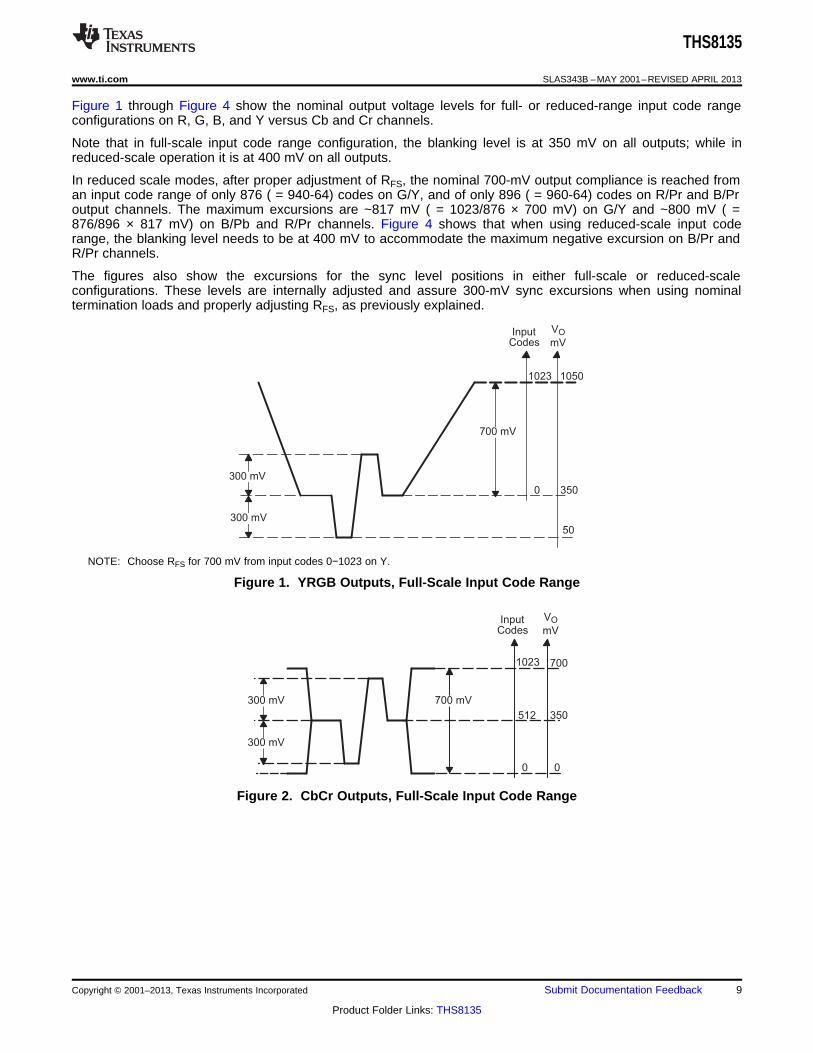
Figure 1 through Figure 4 show the nominal output voltage levels for full- or reduced-range input code rangeconfigurations on R, G, B, and Y versus Cb and Cr channels.
Note that in full-scale input code range configuration, the blanking level is at 350 mV on all outputs; while inreduced-scale operation it is at 400 mV on all outputs.
In reduced scale modes, after proper adjustment of RFS, the nominal 700-mV output compliance is reached froman input code range of only 876 ( = 940-64) codes on G/Y, and of only 896 ( = 960-64) codes on R/Pr and B/Proutput channels. The maximum excursions are ~817 mV ( = 1023/876 × 700 mV) on G/Y and ~800 mV ( =876/896 × 817 mV) on B/Pb and R/Pr channels. Figure 4 shows that when using reduced-scale input coderange, the blanking level needs to be at 400 mV to accommodate the maximum negative excursion on B/Pr andR/Pr channels.
The figures also show the excursions for the sync level positions in either full-scale or reduced-scaleconfigurations. These levels are internally adjusted and assure 300-mV sync excursions when using nominaltermination loads and properly adjusting RFS, as previously explained.
NOTE: Choose RFS for 700 mV from input codes 0−1023 on Y.
Figure 1. YRGB Outputs, Full-Scale Input Code Range
Figure 2. CbCr Outputs, Full-Scale Input Code Range
Copyright © 2001–2013, Texas Instruments Incorporated Submit Documentation Feedback 9
Product Folder Links: THS8135

0
1023
0
700
512 400
50
800
64
960
300 mV
800 mV
700 mV
300 mV
Illegal Color
Difference Outputs
InputCodes
VO
mV
0
0
64
940
1023
400
350
1100
1167
100
InputCodes
VO
mV
300 mV
300 mV
817 mV
700 mV
Super-Black/Super-White
Excursions (Reduced-Scale
Input Code Range)
THS8135
SLAS343B –MAY 2001–REVISED APRIL 2013 www.ti.com
NOTE: Choose RFS for 700 mV from input codes 64−940 on Y.
Figure 3. YRGB Outputs, Reduced-Scale Input Code Range
Figure 4. CbCr Outputs, Reduced-Scale Input Code Range
Output Amplitude Control
The current drive on all three output channels (including sync) is controlled by a resistor RFS that must beconnected between FSADJ and AVSS. In all operation modes the relative amplitudes of these current drivers aremaintained irrespective of the RFS value, as long as a maximum current drive capability is not exceeded.Therefore, a 7:3 video to sync ratio is preserved when adjusting RFS.
The sync generator is composed of different current sources that are internally routed to a corresponding DACoutput. Because they are additional to the video DACs, full 10-bit DAC resolution is preserved for video.Depending on the setting of INS3_INT during SYNC low, the sync current drive is added to either only the greenchannel output (sync-on-G/Y) if INS3_INT = L or all three channel outputs (sync-on-all) if INS3_INT = H. Syncinsertion is only available in video DAC mode.
Figure 5 shows the relationship between RFS and the current drive level on each channel for full-range DACinput. When using reduced-scale range, the codes on the G/Y channel are not internally scaled (only BCb andRCr channels are scaled). Therefore, the user should increase the DAC full-scale current by decreasing RFS by afactor of 1023/(940-64) to map the reduced-scale Y input code range to the same output current drive level.Because these are the current drive levels for the video DACs, they do not take into account the additional dcbias for sync insertion when using video DAC mode. The voltage compliance outputs in Figure 5 assumetermination with a 37.5-Ω resistor.
10 Submit Documentation Feedback Copyright © 2001–2013, Texas Instruments Incorporated
Product Folder Links: THS8135

350
450
550
650
750
850
950
1050
1150
1250
1350
1.8 2.3 2.8 3.3 3.8 4.3 4.8 5.3 5.8 6.3 6.8 7.3
1450
−O
utp
ut V
oltage
−m
V
R(FS) − Full-Scale Resistance − kΩ
VO
Full-Scale DAC Output
Current Adjustment at
37.5-Ω DAC Termination
THS8135
www.ti.com SLAS343B –MAY 2001–REVISED APRIL 2013
Figure 5. Output Voltage vs Full-Scale Resistance
The user is free to connect another resistor value, but care should be taken not to exceed the maximum currentlevel on each of the DAC outputs as shown in the specifications section.
Backward Compatibility With the THS8133
Power Supply
The THS8135 is a functional superset to the THS8133 and is footprint compatible that is a board designed forthe THS8133 can also be used with the THS8135. Both devices come in the same package and have identicalpinouts. Only the power supply levels need to be adjusted as shown in Table 9.
Table 9. Power Supply Changes THS8133 vs THS8135
THS8133 THS8135
AVDD 5 V 3.3 V
DVDD 3.3 V to 5 V 1.8 V
Device Configuration
The THS8135 samples both M1 and M2 on the second rising edge of CLK after a transition on SYNC in videomodes. Depending on the polarity of the transition, M1 is interpreted as either M1_INT or BLK_INT. In theTHS8133 the M1 signal is not sampled but continuously interpreted, and is only interpreted as M1_INT. TheTHS8133 does not offer a reduced-scale input code range configuration and therefore does not requireBLNK_INT.
Only when this additional functionality, which is typical for video systems, is desired, a small change in theconfiguration of the device is required by supplying a dynamically changing signal on M1, generated in a similarway as M2, as shown in Table 10.
Note that this backward compatibility is due to the selection of full-scale versus reduced-scale configurations inTable 7. All configurations that have equal logic levels for BLNK_INT and M1_INT produce full-scale input coderange, which are compatible with the THS8133. This allows the use of a signal tied high or low on M1, as on theTHS8133, for these backward compatible full-scale configurations.
Copyright © 2001–2013, Texas Instruments Incorporated Submit Documentation Feedback 11
Product Folder Links: THS8135

CLK
SYNC
M2
(= SYNC_delayed)
INS3_INT
M2_INT
M2
(= Not SYNC_delayed)]
INS3_INT
M2_INT
if (M2 = SYNC_delayed) → M2_INT = L and INS3_INT = H
if (M2 = NOT SYNC_delayed) → M2_INT = H and INS3_INT = L
THS8135
SLAS343B –MAY 2001–REVISED APRIL 2013 www.ti.com
DAC Outputs
The position of the blanking levels in the THS8135 differs from the position of the blanking levels in theTHS8133. This is to accommodate both full- and reduced-scale configurations on this device, while the THS8133only supported full-scale. When the DAC output is ac-coupled, as is typically the case, there is no change to theoutput video waveform. Typically a clamp circuit at the receiving side will restore the signal to the proper dc level.
Video DAC Mode vs Generic DAC Mode
The THS8133 does not offer a generic DAC mode. The THS8135 uses only the same number of control signalsthan the THS8133 but additionally introduces a generic video mode by specific use of a don’t care signalcombination of these control signals on the THS8133.
Programming Example for M2 (1)
Configuration of the device is normally static in a given application, although it is theoretically possible toreconfigure the device during operation.
If M2_INT and INS3_INT need to be either low or high, the M2 pin is simply tied low or high. If M2_INT andINS3_INT need to have different levels, these can be easily derived from the signal on the SYNC pin, as shownin Table 10 and Figure 6.(1) Programming M1 is analogous.
Table 10. Generating M2 From SYNC
TO HAVE:APPLY TO M2:
M2_INT INS3_INT
L H ... SYNC delayed by two CLK periods
H L ... inverted SYNC delayed by two CLK periods
M1 can be generated similarly. Therefore, at most one inverter and two flip flops are needed to configure any ofthe THS8135 modes using M1 and M2.
Figure 6. Generating INS3_INT and M2_INT From M2
12 Submit Documentation Feedback Copyright © 2001–2013, Texas Instruments Incorporated
Product Folder Links: THS8135

Cb(0) Y(0) Cr(0) Y(2) Cb(4) Y(4) Cr(4) Y(6) Cb(8)
ARPr, AGY, ABPb Output
Corresponding to Cr(0),Y(0), Cb(0)
Data Path Latency = 10.5 CLK Cycles
Cb(0) Registered
BLANK
RCr[9:0]
GY[9:0]
BCb[9:0]
Y(8) Cr(8)
Y(0) Registered
T0 T1 T2 T3 T4 T5 T6 T7 T8CLK T9 T10
First Registered Sample on GY[9:0] after L H on is Interpreted as Cb[9:0]⇒ BLANK
Cr(0) Registered
Y(10)
T11
Cb(0) Cr(0) Cb(2) Cr(2) Cb(4) Cr(4) Cb(6) Cr(6) Cb(8)
Y(0) Y(1) Y(2) Y(3) Y(4) Y(5) Y(6) Y(7) Y(8)
Data Path Latency = 9.5 CLK Cycles
Cb(0), Y(0) Registered
BLANK
RCr[9:0]
GY[9:0]
BCb[9:0]
Cr(8)
Y(9)
Cr(0), Y(1) Registered
T0 T1 T2 T3 T4 T5 T6 T7 T8 T9
First Registered Sample on RCr[9:0] after L H on is Interpreted as Cb[9:0]⇒ BLANK
ARPr, AGY, ABPb Output
Corresponding to Cr(0),Y(0), Cb(0)
Cb(10) Cr(10)
Y(10) Y(11)
T10 T11
T0 T1 T2 T3 T4 T5 T6 T7 T8
RCr(0) RCr(1) RCr(2) RCr(3) RCr(4) RCr(5) RCr(6) RCr(7) RCr(8)
GY(0) GY(1) GY(2) GY(3) GY(4) GY(5) GY(6) GY(7) GY(8)
BCb(0) BCb(1) BCb(2) BCb(3) BCb(4) BCb(5) BCb(6) BCb(7) BCb(8)
ARPr, AGY, ABPb Output
Corresponding to RCr(0), GY(0), BCb(0)
Data Path Latency = 7.5 CLK Cycles
RCr(0), GY(0), BCb(0) Registered
CLK
THS8135
www.ti.com SLAS343B –MAY 2001–REVISED APRIL 2013
Figure 7. Input Format and Latency YCbCr 4:4:4 and GBR 4:4:4 Modes
Figure 8. Input Format and Latency YCbCr 4:2:2 2x10-Bit Mode
Figure 9. Input Format and Latency YCbCr 4:2:2 1x10-Bit Mode
Copyright © 2001–2013, Texas Instruments Incorporated Submit Documentation Feedback 13
Product Folder Links: THS8135

Value
Corresponds
to D(0)
CLK
th
ts
D(0)
td(D) td(D) td(D) td(D)
SYNC
SYNC_T
BLANK
DATA[9:0] D(1)
THS8135
SLAS343B –MAY 2001–REVISED APRIL 2013 www.ti.com
Figure 10 shows how to control the SYNC, SYNC_T, and BLANK signals to generate tri-level sync levels andblanking at the DAC output in video mode. A bi-level (negative) sync can be generated similarly by avoiding thepositive transition on SYNC_T during SYNC low.
Note that on the THS8135 it is required to keep SYNC_T low outside the sync interval to avoid entering thegeneric DAC mode.
Figure 10. Sync and Blanking Generation
14 Submit Documentation Feedback Copyright © 2001–2013, Texas Instruments Incorporated
Product Folder Links: THS8135
THS8135
www.ti.com SLAS343B –MAY 2001–REVISED APRIL 2013
Absolute Maximum Ratings (1)
over operating free-air temperature range (unless otherwise noted)
AVDD to AVSS -0.5 V to 3.6 VVDD Supply voltage
DVDD to DVSS -0.5 V to 2 V
Supply voltage, difference between analog and digital AVDD to DVDD, -0.5 to 0.5 Vsupplies AVSS to DVSS
Digital input voltage range to DVSS -0.5 V to DVDD + 0.5 V
TA Operating free-air temperature range 0°C to 70°C
Tstg Storage temperature range -55°C to 150°C
(1) Stresses beyond those listed under absolute maximum ratings may cause permanent damage to the device. These are stress ratingsonly, and functional operation of the device at these or any other conditions beyond those indicated under recommended operatingconditions is not implied. Exposure to absolute-maximum-rated conditions for extended periods may affect device reliability.
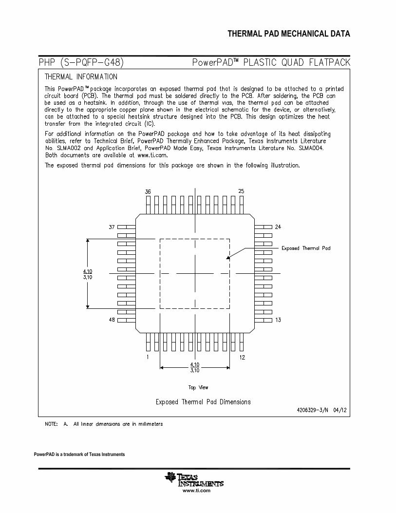
Thermal SpecificationsPARAMETER TEST CONDITIONS (1) MIN TYP MAX UNIT
Thermal PAD soldered to 4-layer High-K 29.11PCBθJA Junction-to-ambient thermal resistance, still air °C/WLow-K PCB, Thermal PAD not soldered 64.42
θJC Junction-to-case thermal resistance, still air 0.12 °C/W
Maximum junction temperature for reliableTJ(MAX) 105 °Coperation
(1) When split ground planes are used, attach the thermal pad to the analog ground plane.
Recommended Operating Conditionsover operating free-air temperature range (unless otherwise noted)
MIN NOM MAX UNIT
Power Supply
AVDD 3 3.3 3.6VDD Supply voltage V
DVDD 1.65 1.8 2
Digital and Reference Inputs
VIH High-level input voltage 1.2 DVDD V
VIL Low-level input voltage DVSS 0.7 V
fclk Clock frequency 0 240 MHz
tw(CLKH) Clock high pulse duration CLK40% 60% period
tw(CLKL) Clock low pulse duration CLK40% 60% period
RFS FSADJ resistor (1) 3.8 kΩ
(1) RFS should be chosen such that the maximum full-scale DAC output current (IFS) does not exceed their maximum stated levels. Thisyields the nominal output voltage compliance at the nominal load termination of 37.5 Ω.
Copyright © 2001–2013, Texas Instruments Incorporated Submit Documentation Feedback 15
Product Folder Links: THS8135

THS8135
SLAS343B –MAY 2001–REVISED APRIL 2013 www.ti.com
Electrical Characteristics
over recommended operating conditions with fCLK = 240 MSPS and use of internal reference voltage VREF, withRFS = RFS(nom) and 37.5-Ω load termination (unless otherwise noted)
Power Supply1 MHz, -1 dBFS digital sine simultaneously applied to all three channels
PARAMETER TEST CONDITIONS MIN TYP MAX UNIT
RGB 89 95 100AVDD = 3.3 V, DVDD = 1.8 V,IAVDD Operating supply current, analog YCbCr 71 76 80 mACLK = 80 MSPS
Generic (700 mV) 63 66 69
RGB 14.5 15.1 15.7AVDD = 3.3 V, DVDD = 1.8 V,IDVDD Operating supply current, digital YCbCr 11.7 12.15 12.7 mACLK = 80 MSPS
Generic (700 mV) 14.64 15.1 15.7
RGB 328 338 350AVDD = 3.3 V, DVDD = 1.8 V,PD Power dissipation YCbCr 262 270 280 mWCLK = 80 MSPS
Generic (700 mV) 237 245 252
RGB 89 95 100AVDD = 3.3 V, DVDD = 1.8 V,IAVDD Operating supply current, analog mACLK = 240 MSPS Generic (700 mV) 63 66 69
RGB 38 40 41AVDD = 3.3 V, DVDD = 1.8 V,IDVDD Operating supply current, digital mACLK = 240 MSPS Generic (700 mV) 38 40 41.1
RGB 373 384 394AVDD = 3.3 V, DVDD = 1.8 V,PD Power dissipation mWCLK = 240 MSPS Generic (700 mV) 281 290 298
AVDD = 3.3 V, DVDD = 1.8 V,IAVDD Operating supply current, analog Generic (1.3 V) 114 mACLK = 80 MSPS
AVDD = 3.3 V, DVDD = 1.8 V,IDVDD Operating supply current, digital Generic (1.3 V) 16 mACLK = 80 MSPS
AVDD = 3.3 V, DVDD = 1.8 V,PD Power dissipation Generic (1.3 V) 405 mWCLK = 80 MSPS
AVDD = 3.3 V, DVDD = 1.8 V,IAVDD Operating supply current, analog Generic (1.3 V) 114 mACLK = 240 MSPS
AVDD = 3.3 V, DVDD = 1.8 V,IDVDD Operating supply current, digital Generic (1.3 V) 41 mACLK = 240 MSPS
AVDD = 3.3 V, DVDD = 1.8 V,PD Power dissipation Generic (1.3 V) 450 mWCLK = 240 MSPS
Digital Inputs – DC CharacteristicsPARAMETER TEST CONDITIONS MIN TYP MAX UNIT
IIH High-level input current 1 µAAVDD = 3.3 V, DVDD = 1.8 V,IIL Low-level input current -1 µADigital inputs and CLK at 0 V for IIL,
IIL(CLK) Low-level input current, CLK -1 1 µADigital inputs and CLK at 2 V for IIHIIH(CLK) High-level input current, CLK -1 1 µA
CI Input capacitance TA = 25°C 5 pF
ts Data and control inputs setup time 2 ns
th Data and control inputs hold time 500 ps
RGB and YCbCr 4:4:4 7.5Digital process delay from first registered color CLKtd(D) YCbCr 4:2:2, 2 x 10 bit 9.5component of pixel (1) periods
YCbCr 4:2:2, 1 x 10 bit 10.5
(1) This parameter is assured by design. The digital process delay is defined as the number of CLK cycles required for the first registeredcolor component of a pixel, starting from the time of registering it on the input bus, to propagate through all processing and appear at theDAC output drivers. The remaining delay through the IC is the analog delay td(A) of the analog output drivers.
16 Submit Documentation Feedback Copyright © 2001–2013, Texas Instruments Incorporated
Product Folder Links: THS8135

THS8135
www.ti.com SLAS343B –MAY 2001–REVISED APRIL 2013
Analog (DAC) OutputsPARAMETER TEST CONDITIONS MIN TYP MAX UNIT
DAC resolution 10 bits
Static, best-fit, sync-on-all, video mode, RGB full-scale -1.1/0.9 -2/1.5
INL Integral nonlinearity Static, best-fit, sync-on-all, video mode, RGB ITU.R-BT601 -1.2/0.8 -2/1.5 LSB
Static, best fit, generic mode, 1.3 V -1.61/0.94 -2/1.5
Static, sync-on-all, video mode, RGB full-scale ±0.4 ±1
DNL Differential nonlinearity Static, sync-on-all, video mode, RGB ITU.R-BT601 ±0.5 ±1 LSB
Static, generic mode, 1.3 V -0.32/0.24
Power supply ripplePSRR rejection ratio of DAC f = DC (1) 38.5 dB
output (full scale)
f = 1 MHz -63Crosstalk betweenXTALK dBchannels (2)f = 30 MHz -39
Voltage referenceVrefo 1.13 1.15 1.16 Voutput
VREF outputRR 276.5 284 294 Ωresistance
Video mode, RGB full-scale -2% 1.8% 2%Imbalance betweenKIMBAL CLK = 80 MSPS (3)DACs Video mode, RGB ITU-R.BT601 -3% 2.8% 3%
Video mode, RGB full-scale 0.7DAC output complianceVOC Video mode, RGB ITU-R.BT601 0.817 Vvoltage (video only) (4)
Generic mode 1.3
AGY 27 28 29.3Video mode, full-scaleRGB, sync-on-all ABPb and ARPr 27 28 29.3
AGY 27 28 29.3Video mode, full-scaleYCbCr, sync-on-all ABPb and ARPr 18 18.67 19.5
IFS CLK = 80 MSPS (5) mAVideo mode, ITU- AGY 30 31.18 32.0R.BT601RGB, sync-on-
ABPb and ARPr 30 31.18 32.3all
Video mode, ITU- AGY 30 31.18 32.1R.BT601 YCbCr, sync-
ABPb and ARPr 20 21.39 22.5on-all
DAC output current risetRDAC CLK = 80 MSPS, 10 to 90% of full-scale 3.2 3.5 4.2 nstime
DAC output current falltFDAC CLK = 80 MSPS, 10 to 90% of full-scale 3.2 3.5 4.2 nstime
Measured from CLK = VIH(min) to 50% of full-scaletd(A) Analog output delay 4 nstransition (6)
Analog output settling Measured from 50% of full scale transition on output totS 15 nstime output settling, within 2% (7)
Spurious-free dynamicSFDR 1 MHz, -1 dBFS digital sine input 55 dBrange
1 dB 50BW Bandwidth MHz
3 dB 100
Eglitch Glitch energy Full-scale code transition at 240 MSPS 25 pVs
(1) PSRR is measured with a 0.1-µF capacitor between the COMP and AVDD pin; with a 0.1-µF capacitor connected between the VREFpin and AVSS. The ripple amplitude is within the range 100 mVp-p to 500 mVp-p with the DAC output set to full scale and a double-terminated 75 Ω (= 37.5 Ω) load. PSRR is defined as 20 x log(ripple voltage at DAC output/ripple voltage at AVDD input). Limits fromcharacterization only.
(2) Crosstalk spec applies to each possible pair of the three DAC outputs. Limits are from characterization only.(3) The imbalance between DACs applies to all possible pairs of the three DACs.(4) Values at RFS = RFS(nom). Limits from characterization only.(5) Values at RFS = RFS(nom).(6) This value excludes the digital process delay, tD(D). Limits from characterization only.(7) Limit from characterization only. Measured on Y channel with other channels not driven.
Copyright © 2001–2013, Texas Instruments Incorporated Submit Documentation Feedback 17
Product Folder Links: THS8135
f − Frequency − MHz
0
100
200
300
400
500
600
0 50 100 150 200 250 300
P−
Pow
er
−m
W
f − Frequency − MHz
300
310
320
330
340
350
360
370
380
390
400
0 50 100 150 200 250 300
P−
Pow
er
−m
W
THS8135
SLAS343B –MAY 2001–REVISED APRIL 2013 www.ti.com
Figure 11. Power vs Clock Frequency, RGB Mode, 1-MHz Input Tone on All Channels
Figure 12. Power vs Clock Frequency, Generic DAC Mode 1.3-V Output, Full-Scale Input Toggle on AllChannels
18 Submit Documentation Feedback Copyright © 2001–2013, Texas Instruments Incorporated
Product Folder Links: THS8135

Input Code
−1.5
−1.0
−0.5
0.0
0.5
1.0
1.5
1 103 205 307 409 511 613 715 817 919 1021
INL
−In
tegra
l N
onlin
earity
−LS
B
Input Code
−0.5
−0.4
−0.3
−0.2
−0.1
0.0
0.1
0.2
0.3
0.4
0.5
1 76 151 226 301 376 451 526 601 676 751 826 901 976 1051
DN
L−
Diffe
rential N
onlin
earity
−LS
B
0.0
THS8135
www.ti.com SLAS343B –MAY 2001–REVISED APRIL 2013
Figure 13. DNL, Generic DAC Mode (1.3-V Output Compliance)
Figure 14. Best-Fit INL, Generic DAC Mode (1.3-V Output Compliance)
Copyright © 2001–2013, Texas Instruments Incorporated Submit Documentation Feedback 19
Product Folder Links: THS8135

f − Frequency − MHz
−6
−5
−4
−3
−2
−1
0
0 10 20 30 40 50 60 70 80 90 100 110 120 130 140 150
Am
plit
ude
−dB
THS8135
SLAS343B –MAY 2001–REVISED APRIL 2013 www.ti.com
Figure 15. Amplitude Response vs Input Frequency at 240 MSPS
20 Submit Documentation Feedback Copyright © 2001–2013, Texas Instruments Incorporated
Product Folder Links: THS8135

THS8135
www.ti.com SLAS343B –MAY 2001–REVISED APRIL 2013
REVISION HISTORY
Revision Comments
SLAS343B Added Thermal Specifications.
Copyright © 2001–2013, Texas Instruments Incorporated Submit Documentation Feedback 21
Product Folder Links: THS8135

PACKAGE OPTION ADDENDUM
www.ti.com 31-May-2013
Addendum-Page 1
PACKAGING INFORMATION
Orderable Device Status(1)
Package Type PackageDrawing
Pins PackageQty
Eco Plan(2)
Lead/Ball Finish MSL Peak Temp(3)
Op Temp (°C) Device Marking(4/5)
Samples
THS8135PHP NRND HTQFP PHP 48 250 Green (RoHS& no Sb/Br)
CU NIPDAU Level-3-260C-168 HR 0 to 70 THS8135
THS8135PHPG4 NRND HTQFP PHP 48 250 Green (RoHS& no Sb/Br)
CU NIPDAU Level-3-260C-168 HR 0 to 70 THS8135
(1) The marketing status values are defined as follows:ACTIVE: Product device recommended for new designs.LIFEBUY: TI has announced that the device will be discontinued, and a lifetime-buy period is in effect.NRND: Not recommended for new designs. Device is in production to support existing customers, but TI does not recommend using this part in a new design.PREVIEW: Device has been announced but is not in production. Samples may or may not be available.OBSOLETE: TI has discontinued the production of the device.
(2) Eco Plan - The planned eco-friendly classification: Pb-Free (RoHS), Pb-Free (RoHS Exempt), or Green (RoHS & no Sb/Br) - please check http://www.ti.com/productcontent for the latest availabilityinformation and additional product content details.TBD: The Pb-Free/Green conversion plan has not been defined.Pb-Free (RoHS): TI's terms "Lead-Free" or "Pb-Free" mean semiconductor products that are compatible with the current RoHS requirements for all 6 substances, including the requirement thatlead not exceed 0.1% by weight in homogeneous materials. Where designed to be soldered at high temperatures, TI Pb-Free products are suitable for use in specified lead-free processes.Pb-Free (RoHS Exempt): This component has a RoHS exemption for either 1) lead-based flip-chip solder bumps used between the die and package, or 2) lead-based die adhesive used betweenthe die and leadframe. The component is otherwise considered Pb-Free (RoHS compatible) as defined above.Green (RoHS & no Sb/Br): TI defines "Green" to mean Pb-Free (RoHS compatible), and free of Bromine (Br) and Antimony (Sb) based flame retardants (Br or Sb do not exceed 0.1% by weightin homogeneous material)
(3) MSL, Peak Temp. -- The Moisture Sensitivity Level rating according to the JEDEC industry standard classifications, and peak solder temperature.
(4) There may be additional marking, which relates to the logo, the lot trace code information, or the environmental category on the device.
(5) Multiple Device Markings will be inside parentheses. Only one Device Marking contained in parentheses and separated by a "~" will appear on a device. If a line is indented then it is a continuationof the previous line and the two combined represent the entire Device Marking for that device.
Important Information and Disclaimer:The information provided on this page represents TI's knowledge and belief as of the date that it is provided. TI bases its knowledge and belief on informationprovided by third parties, and makes no representation or warranty as to the accuracy of such information. Efforts are underway to better integrate information from third parties. TI has taken andcontinues to take reasonable steps to provide representative and accurate information but may not have conducted destructive testing or chemical analysis on incoming materials and chemicals.TI and TI suppliers consider certain information to be proprietary, and thus CAS numbers and other limited information may not be available for release.
In no event shall TI's liability arising out of such information exceed the total purchase price of the TI part(s) at issue in this document sold by TI to Customer on an annual basis.


IMPORTANT NOTICE
Texas Instruments Incorporated and its subsidiaries (TI) reserve the right to make corrections, enhancements, improvements and otherchanges to its semiconductor products and services per JESD46, latest issue, and to discontinue any product or service per JESD48, latestissue. Buyers should obtain the latest relevant information before placing orders and should verify that such information is current andcomplete. All semiconductor products (also referred to herein as “components”) are sold subject to TI’s terms and conditions of salesupplied at the time of order acknowledgment.
TI warrants performance of its components to the specifications applicable at the time of sale, in accordance with the warranty in TI’s termsand conditions of sale of semiconductor products. Testing and other quality control techniques are used to the extent TI deems necessaryto support this warranty. Except where mandated by applicable law, testing of all parameters of each component is not necessarilyperformed.
TI assumes no liability for applications assistance or the design of Buyers’ products. Buyers are responsible for their products andapplications using TI components. To minimize the risks associated with Buyers’ products and applications, Buyers should provideadequate design and operating safeguards.
TI does not warrant or represent that any license, either express or implied, is granted under any patent right, copyright, mask work right, orother intellectual property right relating to any combination, machine, or process in which TI components or services are used. Informationpublished by TI regarding third-party products or services does not constitute a license to use such products or services or a warranty orendorsement thereof. Use of such information may require a license from a third party under the patents or other intellectual property of thethird party, or a license from TI under the patents or other intellectual property of TI.
Reproduction of significant portions of TI information in TI data books or data sheets is permissible only if reproduction is without alterationand is accompanied by all associated warranties, conditions, limitations, and notices. TI is not responsible or liable for such altereddocumentation. Information of third parties may be subject to additional restrictions.
Resale of TI components or services with statements different from or beyond the parameters stated by TI for that component or servicevoids all express and any implied warranties for the associated TI component or service and is an unfair and deceptive business practice.TI is not responsible or liable for any such statements.
Buyer acknowledges and agrees that it is solely responsible for compliance with all legal, regulatory and safety-related requirementsconcerning its products, and any use of TI components in its applications, notwithstanding any applications-related information or supportthat may be provided by TI. Buyer represents and agrees that it has all the necessary expertise to create and implement safeguards whichanticipate dangerous consequences of failures, monitor failures and their consequences, lessen the likelihood of failures that might causeharm and take appropriate remedial actions. Buyer will fully indemnify TI and its representatives against any damages arising out of the useof any TI components in safety-critical applications.
In some cases, TI components may be promoted specifically to facilitate safety-related applications. With such components, TI’s goal is tohelp enable customers to design and create their own end-product solutions that meet applicable functional safety standards andrequirements. Nonetheless, such components are subject to these terms.
No TI components are authorized for use in FDA Class III (or similar life-critical medical equipment) unless authorized officers of the partieshave executed a special agreement specifically governing such use.
Only those TI components which TI has specifically designated as military grade or “enhanced plastic” are designed and intended for use inmilitary/aerospace applications or environments. Buyer acknowledges and agrees that any military or aerospace use of TI componentswhich have not been so designated is solely at the Buyer's risk, and that Buyer is solely responsible for compliance with all legal andregulatory requirements in connection with such use.
TI has specifically designated certain components as meeting ISO/TS16949 requirements, mainly for automotive use. In any case of use ofnon-designated products, TI will not be responsible for any failure to meet ISO/TS16949.
Products Applications
Audio www.ti.com/audio Automotive and Transportation www.ti.com/automotive
Amplifiers amplifier.ti.com Communications and Telecom www.ti.com/communications
Data Converters dataconverter.ti.com Computers and Peripherals www.ti.com/computers
DLP® Products www.dlp.com Consumer Electronics www.ti.com/consumer-apps
DSP dsp.ti.com Energy and Lighting www.ti.com/energy
Clocks and Timers www.ti.com/clocks Industrial www.ti.com/industrial
Interface interface.ti.com Medical www.ti.com/medical
Logic logic.ti.com Security www.ti.com/security
Power Mgmt power.ti.com Space, Avionics and Defense www.ti.com/space-avionics-defense
Microcontrollers microcontroller.ti.com Video and Imaging www.ti.com/video
RFID www.ti-rfid.com
OMAP Applications Processors www.ti.com/omap TI E2E Community e2e.ti.com
Wireless Connectivity www.ti.com/wirelessconnectivity
Mailing Address: Texas Instruments, Post Office Box 655303, Dallas, Texas 75265Copyright © 2013, Texas Instruments Incorporated