sl imx6 ull user guide rev 0 - kontron electronics
TRANSCRIPT


www.kontron-electronics.de // 2
This page has been intentionally left blank
www.kontron-electronics.de // 3
SL IMX6UL/ULL - USER GUIDE
Disclaimer
Kontron Electronics would like to point out that the information contained in this user guide may be subject to alteration,
particularly as a result of the constant upgrading of Kontron Electronics products. This document does not entail any guarantee on
the part of Kontron Electronics with respect to technical processes described in the user guide or any product characteristics set
out in the user guide. Kontron Electronics assumes no responsibility or liability for the use of the described product(s), conveys no
license or title under any patent, copyright or mask work rights to these products and makes no representations or warranties that
these products are free from patent, copyright or mask work right infringement unless otherwise specified. Applications that are
described in this user guide are for illustration purposes only. Kontron Electronics makes no representation or warranty that such
application will be suitable for the specified use without further testing or modification. Kontron Electronics expressly informs the
user that this user guide only contains a general description of processes and instructions which may not be applicable in every
individual case. In cases of doubt, please contact Kontron.
This user guide is protected by copyright. All rights are reserved by Kontron. No part of this document may be reproduced,
transmitted, transcribed, stored in a retrieval system, or translated into any language or computer language, in any form or by any
means (electronic, mechanical, photocopying, recording, or otherwise), without the express written permission of Kontron. Kontron
Electronics points out that the information contained in this user guide is constantly being updated in line with the technical
alterations and improvements made by Kontron Electronics to the products and thus this user guide only reflects the technical
status of the products by Kontron Electronics at the time of publishing.
Brand and product names are trademarks or registered trademarks of their respective owners.
©2021 by Kontron Electronics GmbH
Kontron Electronics GmbH
Kantstr. 10
72663 Großbettlingen
Germany
www.kontron-electronics.de
Kontron Europe GmbH
Gutenbergstr. 2
85737 Ismaning
Germany
www.kontron.com

www.kontron-electronics.de // 4
Intended Use
THIS DEVICE AND ASSOCIATED SOFTWARE ARE NOT DESIGNED, MANUFACTURED OR INTENDED FOR USE OR RESALE
FOR THE OPERATION OF NUCLEAR FACILITIES, THE NAVIGATION, CONTROL OR COMMUNICATION SYSTEMS FOR
AIRCRAFT OR OTHER TRANSPORTATION, AIR TRAFFIC CONTROL, LIFE SUPPORT OR LIFE SUSTAINING APPLICATIONS,
WEAPONS SYSTEMS, OR ANY OTHER APPLICATION IN A HAZARDOUS ENVIRONMENT, OR REQUIRING FAIL-SAFE
PERFORMANCE, OR IN WHICH THE FAILURE OF PRODUCTS COULD LEAD DIRECTLY TO DEATH, PERSONAL INJURY, OR
SEVERE PHYSICAL OR ENVIRONMENTAL DAMAGE (COLLECTIVELY, "HIGH RISK APPLICATIONS").
You understand and agree that your use of Kontron Electronics devices as a component in High Risk Applications is entirely at
your risk. To minimize the risks associated with your products and applications, you should provide adequate design and
operating safeguards. You are solely responsible for compliance with all legal, regulatory, safety, and security related
requirements concerning your products. You are responsible to ensure that your systems (and any Kontron Electronics hardware
or software components incorporated in your systems) meet all applicable requirements. Unless otherwise stated in the product
documentation, the Kontron Electronics device is not provided with error-tolerance capabilities and cannot therefore be deemed
as being engineered, manufactured or setup to be compliant for implementation or for resale as device in High Risk Applications.
All application and safety related information in this document (including application descriptions, suggested safety measures,
suggested Kontron Electronics products, and other materials) is provided for reference only.

www.kontron-electronics.de // 5
Revision History
Revision Brief Description of Changes Date of Issue Author/E
ditor
0.1 Basic draft 2020-February-14 Gb
0.2 Preliminary Version 2020-March-13 Gb/Kl
0.3 Additional information in chapters 5.1.3 and 5.3.2 2020-August-05 Gb
0.4 New address Kontron Headquarter 2021-January-27 Kl
Customer Support
Find Kontron Electronics contacts by visiting: http://www.kontron-electronics.de.
Customer Comments
If you have any difficulties using this user guide, discover an error, or just want to provide some feedback, contact
[email protected]. Detail any errors you find. We will correct the errors or problems as soon as possible and provide
the revised user guide.

www.kontron-electronics.de // 6
Symbols
The following symbols may be used in this user guide
DANGER indicates a hazardous situation which, if not avoided,
will result in death or serious injury.
WARNING indicates a hazardous situation which, if not avoided,
could result in death or serious injury.
NOTICE indicates a property damage message.
CAUTION indicates a hazardous situation which, if not avoided,
may result in minor or moderate injury.
Electric Shock!
This symbol and title warn of hazards due to electrical shocks (> 60 V) when touching products or parts
of products. Failure to observe the precautions indicated and/or prescribed by the law may endanger
your life/health and/or result in damage to your material.
ESD Sensitive Device!
This symbol and title inform that the electronic boards and their components are sensitive to static
electricity. Care must therefore be taken during all handling operations and inspections of this product
in order to ensure product integrity at all times.
HOT Surface!
Do NOT touch! Allow to cool before servicing.
Laser!
This symbol informs of the risk of exposure to laser beam and light emitting devices (LEDs) from an
electrical device. Eye protection per manufacturer notice shall review before servicing.
This symbol indicates general information about the product and the user guide.
This symbol also indicates detail information about the specific product configuration.
This symbol precedes helpful hints and tips for daily use.

www.kontron-electronics.de // 7
Special Handling and Unpacking Instruction
ESD Sensitive Device!
Electronic boards and their components are sensitive to static electricity. Therefore, care must be taken
during all handling operations and inspections of this product, in order to ensure product integrity at all
times.
Do not handle this product out of its protective enclosure while it is not used for operational purposes unless it is otherwise
protected.
Whenever possible, unpack or pack this product only at EOS/ESD safe work stations. Where a safe work station is not guaranteed,
it is important for the user to be electrically discharged before touching the product with his/her hands or tools. This is most
easily done by touching a metal part of your system housing.
It is particularly important to observe standard anti-static precautions when changing piggybacks, ROM devices, jumper settings
etc. If the product contains batteries for RTC or memory backup, ensure that the product is not placed on conductive surfaces,
including anti-static plastics or sponges. They can cause short circuits and damage the batteries or conductive circuits on the
product.
Quality and Environmental Management
Kontron aims to deliver reliable high-end products designed and built for quality, and aims to complying with environmental laws,
regulations, and other environmentally oriented requirements.
For more information regarding Kontron’s quality and environmental responsibilities, visit https://www.kontron-
electronics.de/unternehmen/qualitaet/.
www.kontron-electronics.de // 8
Table of Contents
Symbols .............................................................................................................................................................................................6
Special Handling and Unpacking Instruction .....................................................................................................................................7
Quality and Environmental Management .........................................................................................................................................7
Table of Contents ..............................................................................................................................................................................8
List of Tables ......................................................................................................................................................................................9
List of Figures .....................................................................................................................................................................................9
1/ Introduction ........................................................................................................................................................................10
2/ Description ..........................................................................................................................................................................11
2.1. Product Variants and Accessories .............................................................................................................................................12
3/ System Specifications ..........................................................................................................................................................13
3.1. Component Main Data .............................................................................................................................................................13
3.2. Environmental Conditions ........................................................................................................................................................14
3.3. Functional Block Diagram .........................................................................................................................................................15
4/ Board and Connectors .........................................................................................................................................................16
4.1.1. Connectors.............................................................................................................................................................................16
4.2. Mainboard view and I/O locations ...........................................................................................................................................16
4.3. Bottom Side ..............................................................................................................................................................................17
4.4. Mechanical Drawings ................................................................................................................................................................18
4.5. Pinout of SL iMX6UL/ULL ..........................................................................................................................................................20
4.5.1. Pinout of SL iMX6UL/ULL .......................................................................................................................................................21
5/ Installation ..........................................................................................................................................................................24
5.1. Power Control ...........................................................................................................................................................................24
5.1.1. Power Supply .........................................................................................................................................................................24
5.1.2. Supply voltage .......................................................................................................................................................................24
5.1.3. Supply current .......................................................................................................................................................................24
5.2. Reset pin ...................................................................................................................................................................................24
5.3. Boot Mode ................................................................................................................................................................................25
5.3.1. SD/MMC manufacture mode ................................................................................................................................................25
5.3.2. Serial Downloader .................................................................................................................................................................25
5.4. SD card ......................................................................................................................................................................................26
5.5. Ethernet ....................................................................................................................................................................................26
6/ Thermal considerations .......................................................................................................................................................27
7/ Reflow profile ......................................................................................................................................................................28
8/ Technical Support ...............................................................................................................................................................29
8.1. First Steps – Startup-Information Baseboard ...........................................................................................................................29
8.2. Extended Support .....................................................................................................................................................................29
8.3. Disclaimer & License Information .............................................................................................................................................29
About Kontron Electronics ...............................................................................................................................................................30

www.kontron-electronics.de // 9
List of Tables
Table 1: Product Variants of SL iMX6UL/ULL ...................................................................................................................................12
Table 2: Component Main Data .......................................................................................................................................................13
Table 3: Environmental Conditions..................................................................................................................................................14
Table 4: Connectors of SL iMX6UL/ULL ...........................................................................................................................................16
Table 5: Pinout of SL iMX6UL/ULL castellated pads ........................................................................................................................21
Table 6: Pinout of SL iMX6UL/ULL LGA pads ...................................................................................................................................23
Table 7: Supply voltage ....................................................................................................................................................................24
Table 8: Supply current ....................................................................................................................................................................24
Table 9: Boot mode pin settings ......................................................................................................................................................25
Table 10: Reflow profile ...................................................................................................................................................................28
List of Figures
Figure 1: 25,5x25,5mm SoM with castellation and LGA Pads ..........................................................................................................11
Figure 2: Block Diagram ...................................................................................................................................................................15
Figure 3: Top View ...........................................................................................................................................................................16
Figure 4: Bottom View .....................................................................................................................................................................17
Figure 5: Dimensions of SL iMX6UL/ULL ..........................................................................................................................................18
Figure 6: Thickness from side view ..................................................................................................................................................18
Figure 7: PCB land pattern ...............................................................................................................................................................19
Figure 8: pin assignment ..................................................................................................................................................................20
Figure 9: SD-Card connection example ............................................................................................................................................26
Figure 10: Ethernet connection example ........................................................................................................................................26
Figure 11: Reflow Classification Profile............................................................................................................................................28

SL iMX6UL/ULL - Rev. 0.4
www.kontron-electronics.de // 10
1/ Introduction
This user guide describes the 25,5mmx25,5mm SoM form factor module – SL iMX6UL/ULL. The Advanced RISC Machines (ARM)
based module is equipped with a NXP i.MX6UL/ULL processor. The single core SoC takes advantage of the optimized power
consumption and performance ratio.
The use of this user guide implies a basic knowledge of PC hardware and software. This user guide is focused on describing the
special features and is not intended to be a standard PC textbook. New users are recommended to study the short installation
procedure, before switching on the power.
Latest revision of this user guide, datasheet, and BSPs (Board Support Packages) can be downloaded from Kontron Electronics
Web Page.

SL iMX6UL/ULL - Rev. 0.4
www.kontron-electronics.de // 11
2/ Description
The SL iMX6UL/ULL is a very small System-on-Module (SoM) using NXPs i.MX6UL/ULL processor with ARM Cortex A7. The SL
iMX6UL/ULL is a highly integrated, small sized module for integration in embedded systems with 25,5mmx25,5mm footprint.
The complexity of the DDR3 memory, power management and processor connection are contained in the 8-layer SOM and
simplifies baseboard development.
Figure 1: 25,5x25,5mm SoM with castellation and LGA Pads
Main characteristics of the SL iMX6UL/ULL are:
Single Cortex A7-Core with up to 800 MHz and less than 1 W max power
Up to 1 GB DDR3L memory down
256 to 512 MB SLC NAND-Flash
2 MB QSPI boot flash
Parallel LCD Display up to WXGA (1366x768)
2x USB 2.0 OTG, HS/FS, Device or Host with PHY
2x 10/100 Ethernet with IEEE 1588
6x SPI (including 3 with full duplex I2S)
1x Ethernet 100Mbit with integrated phy
2x 12-bit ADC, up to 10 input channel total, with resistive touch controller (4-wire/5-wire)
multiple GPIOs
8x UART
1x CAN Bus interface (2.0 B)
Please keep in mind, that not all interfaces are available simultaneously due to the amount of port pins and multiple multiplexing
possibilities.

SL iMX6UL/ULL - Rev. 0.4
www.kontron-electronics.de // 12
2.1. Product Variants and Accessories
Following variants are planned:
Table 1: Product Variants of SL iMX6UL/ULL
Board Description Product Number
SL iMX6 UL 256/256 SoM with NXP single core i.MX6 UL G2 processor, 256 MB
DDR3L and 256 MB SLC NAND Flash
40099 123
SL iMX6 UL 512/512 SoM with NXP single core i.MX6 UL G2 processor, 512 MB
DDR3L and 512 MB SLC NAND Flash
40099 122
SL iMX6 ULL 256/256 SoM with NXP single core i.MX6 ULL Y2 processor, 256 MB
DDR3L and 256 MB SLC NAND Flash
40099 144
SL iMX6 ULL 512/512 SoM with NXP single core i.MX6 UL Y2 processor, 512 MB
DDR3L and 512 MB SLC NAND Flash
40099 145
The following accessories are available:
i.MX6 UL Evaluation Kit without display (product no. 50099 061)
i.MX6 UL Evaluation Kit with display (product no. 50099 058)
i.MX6 ULL Evaluation Kit without display (product no. 50099 046)
i.MX6 ULL Evaluation Kit with display (product no. 50099 042)

SL iMX6UL/ULL - Rev. 0.4
www.kontron-electronics.de // 13
3/ System Specifications
3.1. Component Main Data
The table below summarizes the SoM’s features.
Table 2: Component Main Data
SL iMX6UL/ULL
Form factor 25,5x25,5mm with 88 castellated pads and 38 LGA pads
Weight 2g
Processor NXP’s i.MX6 UL/ULL with 9mm x 9mm BGA package in 0.5mm pitch (industrial version)
i.MX6 UL CPU: MCIMX6G2CVK05AB
i.MX6 ULL CPU: MCIMX6Y2CVK08AB
Memory 400 MHz 16-bit DDR3L
256 MByte: 1x 2 Gbit density 128 M x16 DDR3L parts
512 MByte: 1x 4 Gbit density 256 M x16 DDR3L parts
The following memory types are used:
256MByte: Samsung: K4B2G1646F-BMMA
Nanya: NT5CC128M16JR-EKI
Winbond: W632GU6NB11I
Micron: MT41K128M16JT-125 IT:K
512MByte: Samsung: K4B4G1646E-BMMA
Nanya: NT5CC256M16ER-EKI
Intelligent Memory: IM4G16D3FABG-125I
Micron: MT41K256M16TW-107 XIT:P
Boot Flash 1 MB SPI NOR flash in USON (2x3mm) package
Bootloader/BIOS U-Boot Bootloader, Flash for Bootloader connected to ECSPI2
SLC NAND Flash QSPI NAND Flash in WSON 8x6mm package connected on QSPIA
Display 24-bit RGB
Resolution: up to WXGA (1366 x 768) @60 fps
Onboard Controllers
Ethernet Controller 1x 100Mbit PHY KSZ8081RNBIA
Watchdog Timer 3x CPU internal watchdog
System Management
Controller
No dedicated System Management Controller on module System settings can be arranged in U-Boot
environment variables
H/W Status Monitor CPU internal temperature monitoring sensor
Security No security chip on module
Power management No PMIC on module. Discrete power supply is used
Operating System
Support
Linux Yocto
Default Interfaces
I2C 2x I2C interfaces which are derived from the SoC

SL iMX6UL/ULL - Rev. 0.4
www.kontron-electronics.de // 14
LAN, USB 2x 100Mbit-Ethernet
2x USB2.0 OTG
Display 24Bit RGB with up to WXGA (1366 × 768) @60 fps
SD-Card 2x SDIO 4Bit
UART 3x UART, one is used for serial console by default
GPIO 16x General Purpose Inputs/Outputs (GPIO)
PWM 2x from SoC
PWM8: used for Buzzer on baseboard
PWM7: used for TFT backlight on baseboard
other Connectivity 1x CAN
Power
Consumption Maximum Power consumption of the board is < 1 W
Input Voltage Single supply +3.3V
3.2. Environmental Conditions
Table 3: Environmental Conditions
Operating industrial: -40°C to 85°C
relative humidity (non-condensing) 10% to 93% at 40°C
Storage commercial grade: -40°C to +85°C
relative humidity (non-condensing) 10% to 93% at 40°C

SL iMX6UL/ULL - Rev. 0.4
www.kontron-electronics.de // 15
3.3. Functional Block Diagram
The block diagram shows a detailed structure of the SL iMX6UL/ULL module.
Figure 2: Block Diagram
SL iMX6UL/ULL - Rev. 0.4
www.kontron-electronics.de // 16
4/ Board and Connectors
4.1.1. Connectors
Table 4: Connectors of SL iMX6UL/ULL
Connector Function Remark
Castellated pads and LGA
pads
Central Interface solderable
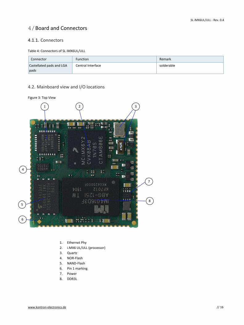
4.2. Mainboard view and I/O locations
Figure 3: Top View
1. Ethernet Phy
2. i.MX6 UL/ULL (processor)
3. Quartz
4. NOR-Flash
5. NAND-Flash
6. Pin 1 marking
7. Power
8. DDR3L
5
3
4
2 1
8
7
6

SL iMX6UL/ULL - Rev. 0.4
www.kontron-electronics.de // 17
4.3. Bottom Side
Figure 4: Bottom View
1. Castellation pads
2. Unique ID
3. LGA pads
4. Test points (factory use only)
1 2 4 3
SL iMX6UL/ULL - Rev. 0.4
www.kontron-electronics.de // 18
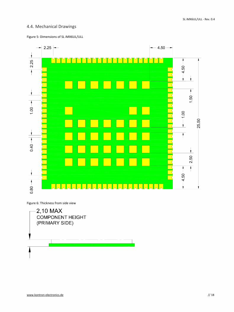
4.4. Mechanical Drawings
Figure 5: Dimensions of SL iMX6UL/ULL
Figure 6: Thickness from side view

SL iMX6UL/ULL - Rev. 0.4
www.kontron-electronics.de // 19
Figure 7: PCB land pattern

SL iMX6UL/ULL - Rev. 0.4
www.kontron-electronics.de // 20
4.5. Pinout of SL iMX6UL/ULL
Figure 8: pin assignment
SL iMX6UL/ULL - Rev. 0.4
www.kontron-electronics.de // 21
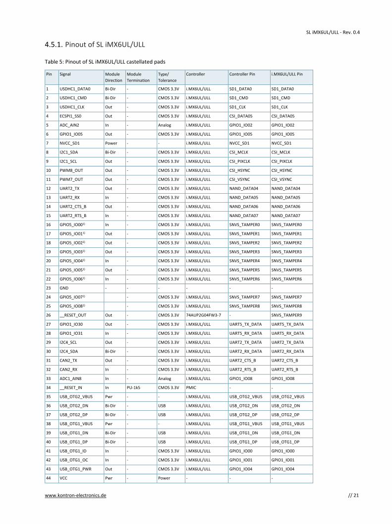
4.5.1. Pinout of SL iMX6UL/ULL
Table 5: Pinout of SL iMX6UL/ULL castellated pads
Pin Signal Module
Direction
Module
Termination
Type/
Tolerance
Controller Controller Pin i.MX6UL/ULL Pin
1 USDHC1_DATA0 Bi-Dir - CMOS 3.3V i.MX6UL/ULL SD1_DATA0 SD1_DATA0
2 USDHC1_CMD Bi-Dir - CMOS 3.3V i.MX6UL/ULL SD1_CMD SD1_CMD
3 USDHC1_CLK Out - CMOS 3.3V i.MX6UL/ULL SD1_CLK SD1_CLK
4 ECSPI1_SS0 Out - CMOS 3.3V i.MX6UL/ULL CSI_DATA05 CSI_DATA05
5 ADC_AIN2 In - Analog i.MX6UL/ULL GPIO1_IO02 GPIO1_IO02
6 GPIO1_IO05 Out - CMOS 3.3V i.MX6UL/ULL GPIO1_IO05 GPIO1_IO05
7 NVCC_SD1 Power - - i.MX6UL/ULL NVCC_SD1 NVCC_SD1
8 I2C1_SDA Bi-Dir - CMOS 3.3V i.MX6UL/ULL CSI_MCLK CSI_MCLK
9 I2C1_SCL Out - CMOS 3.3V i.MX6UL/ULL CSI_PIXCLK CSI_PIXCLK
10 PWM8_OUT Out - CMOS 3.3V i.MX6UL/ULL CSI_HSYNC CSI_HSYNC
11 PWM7_OUT Out - CMOS 3.3V i.MX6UL/ULL CSI_VSYNC CSI_VSYNC
12 UART2_TX Out - CMOS 3.3V i.MX6UL/ULL NAND_DATA04 NAND_DATA04
13 UART2_RX In - CMOS 3.3V i.MX6UL/ULL NAND_DATA05 NAND_DATA05
14 UART2_CTS_B Out - CMOS 3.3V i.MX6UL/ULL NAND_DATA06 NAND_DATA06
15 UART2_RTS_B In - CMOS 3.3V i.MX6UL/ULL NAND_DATA07 NAND_DATA07
16 GPIO5_IO001) In - CMOS 3.3V i.MX6UL/ULL SNVS_TAMPER0 SNVS_TAMPER0
17 GPIO5_IO011) Out - CMOS 3.3V i.MX6UL/ULL SNVS_TAMPER1 SNVS_TAMPER1
18 GPIO5_IO021) Out - CMOS 3.3V i.MX6UL/ULL SNVS_TAMPER2 SNVS_TAMPER2
19 GPIO5_IO031) Out - CMOS 3.3V i.MX6UL/ULL SNVS_TAMPER3 SNVS_TAMPER3
20 GPIO5_IO041) In - CMOS 3.3V i.MX6UL/ULL SNVS_TAMPER4 SNVS_TAMPER4
21 GPIO5_IO051) Out - CMOS 3.3V i.MX6UL/ULL SNVS_TAMPER5 SNVS_TAMPER5
22 GPIO5_IO061) In - CMOS 3.3V i.MX6UL/ULL SNVS_TAMPER6 SNVS_TAMPER6
23 GND - - - - - -
24 GPIO5_IO071) - CMOS 3.3V i.MX6UL/ULL SNVS_TAMPER7 SNVS_TAMPER7
25 GPIO5_IO081) - CMOS 3.3V i.MX6UL/ULL SNVS_TAMPER8 SNVS_TAMPER8
26 __RESET_OUT Out - CMOS 3.3V 74AUP2G04FW3-7 - SNVS_TAMPER9
27 GPIO1_IO30 Out - CMOS 3.3V i.MX6UL/ULL UART5_TX_DATA UART5_TX_DATA
28 GPIO1_IO31 In - CMOS 3.3V i.MX6UL/ULL UART5_RX_DATA UART5_RX_DATA
29 I2C4_SCL Out - CMOS 3.3V i.MX6UL/ULL UART2_TX_DATA UART2_TX_DATA
30 I2C4_SDA Bi-Dir - CMOS 3.3V i.MX6UL/ULL UART2_RX_DATA UART2_RX_DATA
31 CAN2_TX Out - CMOS 3.3V i.MX6UL/ULL UART2_CTS_B UART2_CTS_B
32 CAN2_RX In - CMOS 3.3V i.MX6UL/ULL UART2_RTS_B UART2_RTS_B
33 ADC1_AIN8 In - Analog i.MX6UL/ULL GPIO1_IO08 GPIO1_IO08
34 __RESET_IN In PU-1k5 CMOS 3.3V PMIC - -
35 USB_OTG2_VBUS Pwr - - i.MX6UL/ULL USB_OTG2_VBUS USB_OTG2_VBUS
36 USB_OTG2_DN Bi-Dir - USB i.MX6UL/ULL USB_OTG2_DN USB_OTG2_DN
37 USB_OTG2_DP Bi-Dir - USB i.MX6UL/ULL USB_OTG2_DP USB_OTG2_DP
38 USB_OTG1_VBUS Pwr - - i.MX6UL/ULL USB_OTG1_VBUS USB_OTG1_VBUS
39 USB_OTG1_DN Bi-Dir - USB i.MX6UL/ULL USB_OTG1_DN USB_OTG1_DN
40 USB_OTG1_DP Bi-Dir - USB i.MX6UL/ULL USB_OTG1_DP USB_OTG1_DP
41 USB_OTG1_ID In - CMOS 3.3V i.MX6UL/ULL GPIO1_IO00 GPIO1_IO00
42 USB_OTG1_OC In - CMOS 3.3V i.MX6UL/ULL GPIO1_IO01 GPIO1_IO01
43 USB_OTG1_PWR Out - CMOS 3.3V i.MX6UL/ULL GPIO1_IO04 GPIO1_IO04
44 VCC Pwr - Power - - -

SL iMX6UL/ULL - Rev. 0.4
www.kontron-electronics.de // 22
Pin Signal Module
Direction
Module
Termination
Type/
Tolerance
Controller Controller Pin i.MX6UL/ULL Pin
45 VCC Power - - - - -
46 UART1_TX Out - CMOS 3.3V i.MX6UL/ULL UART1_TX_DATA UART1_TX_DATA
47 UART1_RX In - CMOS 3.3V i.MX6UL/ULL UART1_RX_DATA UART1_RX_DATA
48 UART1_CTS_B Out - CMOS 3.3V i.MX6UL/ULL UART1_CTS_B UART1_CTS_B
49 UART1_RTS_B In - CMOS 3.3V i.MX6UL/ULL UART1_RTS_B UART1_RTS_B
50 ADC1_IN3 In - Analog i.MX6UL/ULL GPIO1_IO03 GPIO1_IO03
51 VDD_SNVS_IN Power - - i.MX6UL/ULL VDD_SNVS_IN VDD_SNVS_IN
52 UART4_TX2) Out - CMOS 3.3V i.MX6UL/ULL UART4_TX_DATA UART4_TX_DATA
53 UART4_RX2) In - CMOS 3.3V i.MX6UL/ULL UART4_RX_DATA UART4_RX_DATA
54 GPIO1_IO24 In - CMOS 3.3V i.MX6UL/ULL UART3_TX_DATA UART3_TX_DATA
55 GPIO1_IO25 In - CMOS 3.3V i.MX6UL/ULL UART3_RX_DATA UART3_RX_DATA
56 GPIO1_IO26 In - CMOS 3.3V i.MX6UL/ULL UART3_CTS_B UART3_CTS_B
57 GPIO1_IO27 In - CMOS 3.3V i.MX6UL/ULL UART3_RTS_B UART3_RTS_B
58 ENET1_MDC Out - CMOS 3.3V i.MX6UL/ULL GPIO1_IO07 GPIO1_IO07
59 ENET1_MDIO Bi-Dir PU-1k0 CMOS 3.3V i.MX6UL/ULL GPIO1_IO06 GPIO1_IO06
60 ETH1_RXM Bi-Dir - PHY KSZ8081RNB RXM RMII
61 ETH1_RXP Bi-Dir - PHY KSZ8081RNB RXP RMII
62 ETH1_TXM Bi-Dir - PHY KSZ8081RNB TXM RMII
63 ETH1_TXP Bi-Dir - PHY KSZ8081RNB TXP RMII
64 ETH1_LED0 Out/OD - CMOS 3.3V KSZ8081RNB LED0/NWAYEN RMII
65 ETH1_LED1 Out/OD - CMOS 3.3V KSZ8081RNB LED1/SPEED RMII
66 GND - - - - -
67 ENET2_REF_CLK2 Out - CMOS 3.3V i.MX6UL/ULL ENET2_TX_CLK ENET2_TX_CLK
68 ENET2_RX_ER In - CMOS 3.3V i.MX6UL/ULL ENET2_RX_ER ENET2_RX_ER
69 ENET2_TDATA1 Out - CMOS 3.3V i.MX6UL/ULL ENET2_TX_DATA1 ENET2_TX_DATA1
70 ENET2_RDATA0 In - CMOS 3.3V i.MX6UL/ULL ENET2_RX_DATA0 ENET2_RX_DATA0
71 ENET2_TX_EN Out - CMOS 3.3V i.MX6UL/ULL ENET2_TX_EN ENET2_TX_EN
72 ENET2_TDATA0 Out - CMOS 3.3V i.MX6UL/ULL ENET2_TX_DATA0 ENET2_TX_DATA0
73 ENET2_RDATA1 In - CMOS 3.3V i.MX6UL/ULL ENET2_RX_DATA1 ENET2_RX_DATA1
74 ENET2_RX_EN In - CMOS 3.3V i.MX6UL/ULL ENET2_RX_EN ENET2_RX_EN
75 USDHC2_DATA3 Bi-Dir - CMOS 3.3V i.MX6UL/ULL NAND_DATA03 NAND_DATA03
76 USDHC2_DATA2 Bi-Dir - CMOS 3.3V i.MX6UL/ULL NAND_DATA02 NAND_DATA02
77 USDHC2_DATA1 Bi-Dir - CMOS 3.3V i.MX6UL/ULL NAND_DATA01 NAND_DATA01
78 USDHC2_DATA0 Bi-Dir - CMOS 3.3V i.MX6UL/ULL NAND_DATA00 NAND_DATA00
79 USDHC2_CMD Bi-Dir - CMOS 3.3V i.MX6UL/ULL NAND_WE_B NAND_WE_B
80 USDHC2_CLK Out - CMOS 3.3V i.MX6UL/ULL NAND_RE_B NAND_RE_B
81 USDHC2_RESET Out - CMOS 3.3V i.MX6UL/ULL NAND_ALE NAND_ALE
82 ECSPI1_MISO In - CMOS 3.3V i.MX6UL/ULL CSI_DATA07 CSI_DATA07
83 ECSPI1_MOSI Out - CMOS 3.3V i.MX6UL/ULL CSI_DATA06 CSI_DATA06
84 ECSPI1_SCLK Out - CMOS 3.3V i.MX6UL/ULL CSI_DATA04 CSI_DATA04
85 USDHC1_DATA3 Bi-Dir - CMOS 3.3V i.MX6UL/ULL SD1_DATA3 SD1_DATA3
86 USDHC1_DATA2 Bi-Dir - CMOS 3.3V i.MX6UL/ULL SD1_DATA2 SD1_DATA2
87 USDHC1_DATA1 Bi-Dir - CMOS 3.3V i.MX6UL/ULL SD1_DATA1 SD1_DATA1
88 GND - - - - - -
1) Pins are connected to the RTC supply (SNVS_IN) and can influence RTC power consumption. See Chapter 4.4, AN5170.pdf by NXP 2) Used as Linux console

SL iMX6UL/ULL - Rev. 0.4
www.kontron-electronics.de // 23
Table 6: Pinout of SL iMX6UL/ULL LGA pads
Pin Signal Module
Direction
Module
Termination
Type/
Tolerance
Controller Controller Pin i.MX6UL/ULL Pin
A1 LCDIF_DATA6 Out - CMOS 3.3V i.MX6UL/ULL LCD_DATA06 LCD_DATA06
A2 LCDIF_DATA13 Out - CMOS 3.3V i.MX6UL/ULL LCD_DATA13 LCD_DATA13
A3 LCDIF_DATA20 Out - CMOS 3.3V i.MX6UL/ULL LCD_DATA20 LCD_DATA20
A4 LCDIF_VSYNC Out - CMOS 3.3V i.MX6UL/ULL LCD_VSYNC LCD_VSYNC
A5 BOOT_MODE1 In - CMOS 3.3V i.MX6UL/ULL BOOT_MODE1 BOOT_MODE1
A7 BOOT_MODE0 In - CMOS 3.3V i.MX6UL/ULL BOOT_MODE0 BOOT_MODE0
B1 LCDIF_DATA5 Out - CMOS 3.3V i.MX6UL/ULL LCD_DATA05 LCD_DATA05
B2 LCDIF_DATA12 Out - CMOS 3.3V i.MX6UL/ULL LCD_DATA12 LCD_DATA12
B3 LCDIF_DATA19 Out - CMOS 3.3V i.MX6UL/ULL LCD_DATA19 LCD_DATA19
B4 LCDIF_HSYNC Out - CMOS 3.3V i.MX6UL/ULL LCD_HSYNC LCD_HSYNC
B5 ONOFF In - CMOS 3.3V i.MX6UL/ULL ONOFF ONOFF
B7 JTAG_TRST_B In - CMOS 3.3V i.MX6UL/ULL JTAG_TRST_B JTAG_TRST_B
C1 LCDIF_DATA4 Out - CMOS 3.3V i.MX6UL/ULL LCD_DATA04 LCD_DATA04
C2 LCDIF_DATA11 Out - CMOS 3.3V i.MX6UL/ULL LCD_DATA11 LCD_DATA11
C3 LCDIF_DATA18 Out - CMOS 3.3V i.MX6UL/ULL LCD_DATA18 LCD_DATA18
C4 LCDIF_CLK Out - CMOS 3.3V i.MX6UL/ULL LCD_CLK LCD_CLK
C7 JTAG_TCK In - CMOS 3.3V i.MX6UL/ULL JTAG_TCK JTAG_TCK
D1 LCDIF_DATA3 Out - CMOS 3.3V i.MX6UL/ULL LCD_DATA03 LCD_DATA03
D2 LCDIF_DATA10 Out - CMOS 3.3V i.MX6UL/ULL LCD_DATA10 LCD_DATA10
D3 LCDIF_DATA17 Out - CMOS 3.3V i.MX6UL/ULL LCD_DATA17 LCD_DATA17
D4 LCDIF_ENABLE Out - CMOS 3.3V i.MX6UL/ULL LCD_ENABLE LCD_ENABLE
D7 JTAG_TDI In - CMOS 3.3V i.MX6UL/ULL JTAG_TDI JTAG_TDI
E1 LCDIF_DATA2 Out - CMOS 3.3V i.MX6UL/ULL LCD_DATA02 LCD_DATA02
E2 LCDIF_DATA9 Out - CMOS 3.3V i.MX6UL/ULL LCD_DATA09 LCD_DATA09
E3 LCDIF_DATA16 Out - CMOS 3.3V i.MX6UL/ULL LCD_DATA16 LCD_DATA16
E4 LCDIF_DATA23 Out - CMOS 3.3V i.MX6UL/ULL LCD_DATA23 LCD_DATA23
E7 JTAG_TDO Out - CMOS 3.3V i.MX6UL/ULL JTAG_TDO JTAG_TDO
F1 LCDIF_DATA1 Out - CMOS 3.3V i.MX6UL/ULL LCD_DATA01 LCD_DATA01
F2 LCDIF_DATA8 Out - CMOS 3.3V i.MX6UL/ULL LCD_DATA08 LCD_DATA08
F3 LCDIF_DATA15 Out - CMOS 3.3V i.MX6UL/ULL LCD_DATA15 LCD_DATA15
F4 LCDIF_DATA22 Out - CMOS 3.3V i.MX6UL/ULL LCD_DATA22 LCD_DATA22
F7 JTAG_TMS Bi-Dir - CMOS 3.3V i.MX6UL/ULL JTAG_TMS JTAG_TMS
G1 LCDIF_DATA0 Out - CMOS 3.3V i.MX6UL/ULL LCD_DATA00 LCD_DATA00
G2 LCDIF_DATA7 Out - CMOS 3.3V i.MX6UL/ULL LCD_DATA07 LCD_DATA07
G3 LCDIF_DATA14 Out - CMOS 3.3V i.MX6UL/ULL LCD_DATA14 LCD_DATA14
G4 LCDIF_DATA21 Out - CMOS 3.3V i.MX6UL/ULL LCD_DATA21 LCD_DATA21
G5 LCDIF_RESET Out - CMOS 3.3V i.MX6UL/ULL LCD_RESET LCD_RESET
G7 JTAG_MOD Out PD-4k75 CMOS 3.3V i.MX6UL/ULL JTAG_MOD JTAG_MOD

SL iMX6UL/ULL - Rev. 0.4
www.kontron-electronics.de // 24
5/ Installation
5.1. Power Control
5.1.1. Power Supply
The SoM can be powered from a single 3.3V power Source at VCC pins. The VDD_SNVS_IN pin can be connected to an external
battery. If no external battery is used, it is mandatory to connect this pin to VCC.
NVCC_SD1 is used to power the SDIO1 interface. If UHS‐I mode is used, card voltage must be lowered to 1.8 V according to pin
SDIO1_VSELECT. If UHS-I mode is not used, NVCC_SD1 can be connected to VCC.
Small decoupling capacitors like 100nF should be used for each supply pin an should be placed as close as possible.
If USB is unused VBUS can be left floating. Otherwise connect VBUS to +5 V.
5.1.2. Supply voltage
Table 7: Supply voltage
Voltage nominal min max
VCC 3.3 V 3.0 V 3.6 V
VDD_SNVS_IN 3.3 V 2.4 V 3.6 V
USB_OTG1/2_VBUS 5.0 V 4.4 V 5.5 V
NVCC_SD1 3.3/1.8 V 1.65 V 3.6 V
5.1.3. Supply current
Table 8: Supply current
Use case mean max
Linux running 110 mA -
A7 heavy load 190 mA 260 mA
At power on, the SoM can cause a current spike of up to 1.5 A for 5 µs. Make sure to have a low
impedance path from the supply to the SoM or enough capacity to buffer the spike, otherwise the
resulting voltage drop will lead to male function.
5.2. Reset pin
A low level at __RESET_IN triggers a reset. The module will stay in reset as long as __RESET_IN is grounded. If unused, this pin can
be left floating. No external components are required.
The following parameters should be delivered from the carrier board:
Voltage Ripple maximum 100 mV peak to peak 0-20 MHz, 20 ms rise
time from input voltage <10% to nominal VCC

SL iMX6UL/ULL - Rev. 0.4
www.kontron-electronics.de // 25
5.3. Boot Mode
The device has four boot modes (one is reserved for NXP use).
Table 9: Boot mode pin settings
BOOT_MODE[1:0] Boot Type
00 Boot From Fuses
01 Serial Downloader
10 Internal Boot
11 Reserved
BOOT_MODE[1:0] pins have internal pull-downs. By default, these pins can be left floating to stay in “Boot from Fuses” mode. In
this mode the SoM boots as programmed by Kontron.
5.3.1. SD/MMC manufacture mode
If no valid boot image is found on the programmed boot devices the SoM switches to SD/MMC manufacture mode before the
serial download mode. In the manufacture mode, the SD or MMC card will be scanned on the uSDHC1. If a card is detected and a
valid boot image is found in the card, the boot image is loaded and executed. Pad 49 of the SoM acts as SD1_CD and is used to
detect whether a card is inserted or not.
5.3.2. Serial Downloader
The Serial Downloader provides a means to download a program image to the chip over the USB OTG1 or UART 1/2 serial
connection.
It is recommended to have the boot pins and the OTG1 pins available on the baseboard to recover the
SoM in case of a broken image. In addition, also the SD1 pins including the SD1_CD pin and the pins for
the Linux console can be useful.

SL iMX6UL/ULL - Rev. 0.4
www.kontron-electronics.de // 26
5.4. SD card
Figure 9: SD-Card connection example
5.5. Ethernet
The SL iMX6UL/ULL includes the 100Mbit Phy KSZ8081RNBIA. This makes the ethernet implementation on the baseboard quite
simple. Only an appropriate connector with magnetics has to be connected.
Figure 10: Ethernet connection example

SL iMX6UL/ULL - Rev. 0.4
www.kontron-electronics.de // 27
6/ Thermal considerations
The temperature rise of the CPU depends on the use case and varies from 20°C for “Linux running” up to approximately 45°C for
“A7 heavy load”.
Due to the maximum temperature of 105°C of the SoC a cooling concept should be considered depending on the CPU load and the
maximum ambient temperature.

SL iMX6UL/ULL - Rev. 0.4
www.kontron-electronics.de // 28
7/ Reflow profile
Table 10: Reflow profile
Profile Feature Pb-Free Assembly
Average Ramp-Up Rate (TSMAX to TP) 3°C/second max.
Preheat
Temperature Min (TSMIN)
Temperature Max (TSMAX)
Time (ts) from (TSMIN to TSMAX)
150 °C
200 °C
60-120 seconds
Liquidous temperature (TL)
Time (tL) maintained above TL
217 °C
60-80 seconds
Peak/Classification Temperature (TP) 250 °C
Time within 5 °C of actual peak temperature (tP) 20 seconds
Ramp-down rate 6°C/second max
Time 25 °C to peak temperature 8 minutes max
Figure 11: Reflow Classification Profile
To minimize the stress for the components, it is strongly recommended to solder the SoM during the last reflow cycle of the
carrier board manufacturing process.
SL iMX6UL/ULL - Rev. 0.4
www.kontron-electronics.de // 29
8/ Technical Support
8.1. First Steps – Startup-Information Baseboard
For the first startup of your Board, which includes the SL iMX6UL/ULL SoM, you will find more information about the Software /
BSP and additional hardware information at the online documentation.
Please follow the link https://docs.kontron-electronics.de/yocto-ktn/build-ktn-rocko/
The online documentation is primarily intended for our Eval-Kit / Evalboard, but will help you also to put your board into
operation. Additionally, you will find information how to get access to the Yocto based GitLab software repository and how to
make your own software images.
8.2. Extended Support
For detailed technical support please contact:
E-Mail: [email protected]
8.3. Disclaimer & License Information
The software contained in the device (BSP) contains parts which were licensed as free respectively open source software under
the GNU General Public License, version 2 and/or 3, respectively the GNU Lesser General Public License, versions 2.1 and/or 3.0.
You can obtain a copy of the source code of the BSP by following the instructions in the manual at https://docs.kontron-
electronics.de/build-system or contact:
Kontron Electronics GmbH
Kantstr. 10
72663 Großbettlingen
Germany
Web: www.kontron-electronics.de
E-Mail: [email protected]
SL iMX6UL/ULL - Rev. 0.4
www.kontron-electronics.de // 30
About Kontron Electronics
Kontron Electronics is your complete supplier of electronics and automation solutions. We offer
own control products for the automation of machines and devices,
Development and production for individual, complex electronic modules
Production services for your existing electronic assemblies
Assembly services for complete systems
With our existing control, visualisation and automation systems, we can put together turnkey complete solutions for your machines and
equipment in the shortest possible time.
For your individual requirements we have a large group of engineers and technicians available, who develop your tailor-made solution with a lot of
experience and imagination.
Kontron Electronics is a full-service provider for the development and production of complex electronic modules, components and systems for
industrial and medical applications.
Kontron Electronics GmbH
Kantstraße 10 72663 Großbettlingen Germany Tel.: + 49 7022 4057-0 Fax: + 49 7022 4057-22 [email protected]