skywire ® embedded cellular modem datasheet power consumption - nl-sw-hspa 8 mechanical...
TRANSCRIPT

Skywire® HSPA+ HE910
Embedded Cellular Modem
Datasheet
NimbeLink Corp Updated: May 2018
PN 30026 rev 11 © NimbeLink Corp. 2018. All rights reserved. 1

Table of Contents
Table of Contents 2
Introduction 4 Orderable Part Numbers 4 Additional Resources 4 Product Overview 4 Block Diagram 5
Technical Specifications 6 Electrical Specifications 6
Absolute Maximum Ratings 6 Recommended Ratings & Module Pin out 6 Connectors J1 and J2 6 Connectors J3, X1, X2, X3 7 Typical Power Consumption - NL-SW-HSPA 8
Mechanical Specifications 9 Mechanical Characteristics 9 Mating Connectors 9 Device Placement 9
Environmental Specifications 9
Important Design Considerations 10 ON_OFF Signal 10 Power Monitoring 10 AT#GPIO=2,1,1,1 11 Power Supply Requirements 11 Serial Communications 11
Mounting Guidelines 13 Board to Board connectors approach 13 Solder to Board connection approach 14
Antenna Considerations 15 Primary Antenna Requirements 15 Diversity Antenna Requirements 15 GPS Antenna Requirements 16 Recommended Antennas 16
PN 30026 rev 11 © NimbeLink Corp. 2018. All rights reserved. 2
Certifications 18 Carrier Specific 18 Geography Specific 18
Federal Regulatory Licensing 18
End Product Labeling Requirements 18
PN 30026 rev 11 © NimbeLink Corp. 2018. All rights reserved. 3

1. Introduction
1.1 Orderable Part Numbers
Orderable Device
Telit Chipset
Operating Temperature Bands
Fallback?
Network Type GPS
NL-SW-HSPA HE910-DG -40 to +85˚C B1, B2, B4, B5, B6, B8 Yes GSM Yes
NL-SW-HSPAP HE910-NAD -40 to +85˚C B2, B4, B5, B6 Yes GSM No
NL-SW-HSPAPG HE910-NAG -40 to +85˚C B2, B4, B5, B6 Yes GSM Yes
NL-SW-HSPAPE HE910-EU -40 to +85˚C B1, B5, B6, B8 Yes GSM Yes
1.2 Additional Resources The following documents or documentation resources are referenced within this document. ● NL-SW-HSPA Product Page ● GPS & Assisted GPS App Note ● Sending and Receiving data with Socket Dials ● Prototyping considerations App Note
1.3 Product Overview Add robust cellular connectivity to your M2M devices with scalable radio technology with Skywire line of modems including HE910 based HSPA+ solutions. Extensive experience in designing and building embedded product solutions makes the NimbeLink Skywire® embedded cellular modem the smallest on the market. It uses the popular Skywire interface and supports multiple GSM bands and fallback capability minimizing costs of hardware and network access. The module is designed for volume production and is intended for OEMs to embed into end equipment designs.
PN 30026 rev 11 © NimbeLink Corp. 2018. All rights reserved. 4

1.4 Block Diagram
PN 30026 rev 11 © NimbeLink Corp. 2018. All rights reserved. 5
2. Technical Specifications
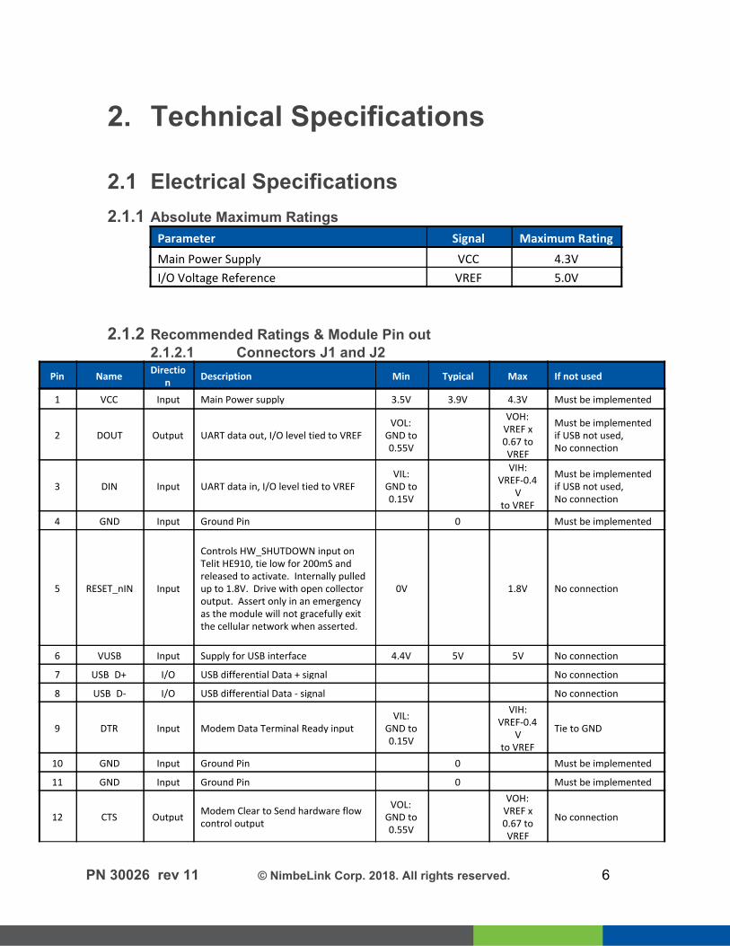
2.1 Electrical Specifications 2.1.1 Absolute Maximum Ratings
Parameter Signal Maximum Rating Main Power Supply VCC 4.3V I/O Voltage Reference VREF 5.0V
2.1.2 Recommended Ratings & Module Pin out 2.1.2.1 Connectors J1 and J2
Pin Name Direction Description Min Typical Max If not used
1 VCC Input Main Power supply 3.5V 3.9V 4.3V Must be implemented
2 DOUT Output UART data out, I/O level tied to VREF VOL:
GND to 0.55V
VOH:
VREF x 0.67 to VREF
Must be implemented if USB not used, No connection
3 DIN Input UART data in, I/O level tied to VREF VIL:
GND to 0.15V
VIH:
VREF-0.4V
to VREF
Must be implemented if USB not used, No connection
4 GND Input Ground Pin 0 Must be implemented
5 RESET_nIN Input
Controls HW_SHUTDOWN input on Telit HE910, tie low for 200mS and released to activate. Internally pulled up to 1.8V. Drive with open collector output. Assert only in an emergency as the module will not gracefully exit the cellular network when asserted.
0V 1.8V No connection
6 VUSB Input Supply for USB interface 4.4V 5V 5V No connection 7 USB_D+ I/O USB differential Data + signal No connection 8 USB_D- I/O USB differential Data - signal No connection
9 DTR Input Modem Data Terminal Ready input VIL:
GND to 0.15V
VIH:
VREF-0.4V
to VREF Tie to GND
10 GND Input Ground Pin 0 Must be implemented 11 GND Input Ground Pin 0 Must be implemented
12 CTS Output Modem Clear to Send hardware flow control output
VOL: GND to 0.55V
VOH:
VREF x 0.67 to VREF
No connection
PN 30026 rev 11 © NimbeLink Corp. 2018. All rights reserved. 6
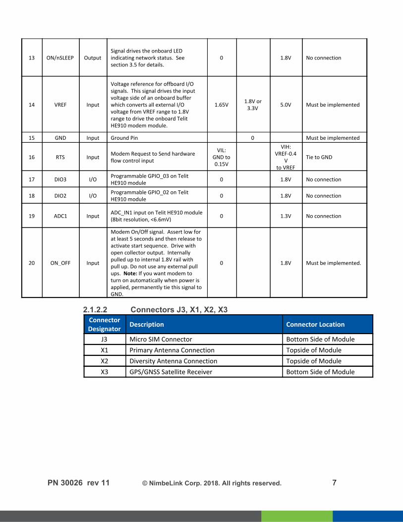
13 ON/nSLEEP Output Signal drives the onboard LED indicating network status. See section 3.5 for details.
0 1.8V No connection
14 VREF Input
Voltage reference for offboard I/O signals. This signal drives the input voltage side of an onboard buffer which converts all external I/O voltage from VREF range to 1.8V range to drive the onboard Telit HE910 modem module.
1.65V 1.8V or 3.3V 5.0V Must be implemented
15 GND Input Ground Pin 0 Must be implemented
16 RTS Input Modem Request to Send hardware flow control input
VIL: GND to 0.15V
VIH:
VREF-0.4V
to VREF Tie to GND
17 DIO3 I/O Programmable GPIO_03 on Telit HE910 module 0 1.8V No connection
18 DIO2 I/O Programmable GPIO_02 on Telit HE910 module 0 1.8V No connection
19 ADC1 Input ADC_IN1 input on Telit HE910 module (8bit resolution, <6.6mV) 0 1.3V No connection
20 ON_OFF Input
Modem On/Off signal. Assert low for at least 5 seconds and then release to activate start sequence. Drive with open collector output. Internally pulled up to internal 1.8V rail with pull up. Do not use any external pull ups. Note: If you want modem to turn on automatically when power is applied, permanently tie this signal to GND.
0 1.8V Must be implemented.
2.1.2.2 Connectors J3, X1, X2, X3 Connector Designator Description Connector Location
J3 Micro SIM Connector Bottom Side of Module X1 Primary Antenna Connection Topside of Module X2 Diversity Antenna Connection Topside of Module X3 GPS/GNSS Satellite Receiver Bottom Side of Module
PN 30026 rev 11 © NimbeLink Corp. 2018. All rights reserved. 7

2.1.3 Typical Power Consumption - NL-SW-HSPA
Measurement Attenuation (dB) AT+CSQ
Average Current
(mA) Peak Current
(mA) Average
Charge (μAh) Notes
Socket Dial 0 18 106.391 228.14 386.07
Tested at 3.8V Time elapsed: 12.565s Test: Opening socket, making HTTP POST, reading HTTP response, closing socket, powering off Skywire.
Socket Dial 20 10 116.74 246.35 390.753
Tested at 3.8V Time elapsed: 12.322s Test: Opening socket, making HTTP POST, reading HTTP response, closing socket, powering off Skywire.
Socket Dial 40 1 152.03 622.075 594.341
Tested at 3.8V Time elapsed: 12.507s Test: Opening socket, making HTTP POST, reading HTTP response, closing socket, powering off Skywire.
Off 0 - 2.64 3.01 660.68 Tested at 3.8V Connected to power, not turned on. 15 minute sample.
Idle - Low Power 0 - 7.91 85.795 1990.34
Tested at 3.8V 15 minute sample period. AT+CFUN=5, DTR held HIGH.
Idle 0 - 19.3 114.60 4820.16 Tested at 3.8V Registered on network, 15 minute sample period.
PN 30026 rev 11 © NimbeLink Corp. 2018. All rights reserved. 8
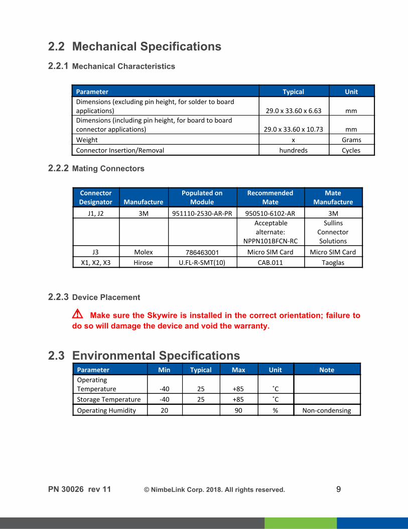
2.2 Mechanical Specifications 2.2.1 Mechanical Characteristics
Parameter Typical Unit Dimensions (excluding pin height, for solder to board applications) 29.0 x 33.60 x 6.63 mm Dimensions (including pin height, for board to board connector applications) 29.0 x 33.60 x 10.73 mm Weight x Grams Connector Insertion/Removal hundreds Cycles
2.2.2 Mating Connectors
Connector Designator Manufacture
Populated on Module
Recommended Mate
Mate Manufacture
J1, J2 3M 951110-2530-AR-PR 950510-6102-AR 3M
Acceptable alternate:
NPPN101BFCN-RC
Sullins Connector Solutions
J3 Molex 786463001 Micro SIM Card Micro SIM Card X1, X2, X3 Hirose U.FL-R-SMT(10) CAB.011 Taoglas
2.2.3 Device Placement
⚠ Make sure the Skywire is installed in the correct orientation; failure to do so will damage the device and void the warranty.
2.3 Environmental Specifications Parameter Min Typical Max Unit Note
Operating Temperature -40 25 +85 ˚C
Storage Temperature -40 25 +85 ˚C
Operating Humidity 20 90 % Non-condensing
PN 30026 rev 11 © NimbeLink Corp. 2018. All rights reserved. 9
3. Important Design Considerations 3.1 ON_OFF Signal
The ON_OFF signal on pin 20 is used to trigger the modem to turn on and to turn the modem off. To conserve power, the onboard cellular module does not automatically startup when power is applied. The baseboard design must supply a means to assert the ON_OFF signal low for at least 5 seconds, then released to start up the modem. The ON_OFF signal should be driven with an open collector output or with an open collector transistor. The signal is internally pulled up and should not be driven high, as doing so may prevent the modem from booting. The modem can be configured to automatically start when power is applied. This can be done by tying the ON_OFF signal to GND (either directly or through a pulldown resistor). However, doing so does run the risk of the modem attempting to boot before the input voltage to the modem is >3.20V, which could cause the modem to lock up. If lock up occurs, the nRESET pin should be asserted to force the modem to initiate a restart. For optimal control of the cellular modem, it is recommended that the system designer control the ON_OFF signal from their host platform using an open collector output or external discrete open collector transistor. The modem will be ready to accept AT commands 2 seconds (average) after the 5 second ON_OFF signal toggle has been released. Users may also use one of the modems GPIO pins as a power monitoring pin as described in section 4.1. The modem will be ready to accept AT commands 1 second after the power monitoring pin as gone high. To turn the modem off via the ON_OFF signal drive the ON_OFF Signal low for at least 3 seconds when the modem is on.
3.2 Power Monitoring Applications can monitor if the modem has powered up by configuring one of the modem’s GPIO pins as an output, set to a high logic state. This output will output a 1.8V signal when the modem’s internal power rail has powered up and go to 0V when the modem shuts down. To configure the modem to use one of its GPIO's as a power monitor, issue the following command: Issue the following AT command to configure pin 17 (GPIO 3) to output a high logic signal and save the setting across reboots:
AT#GPIO=3,1,1,1 Issue the following AT command to configure pin 18 (GPIO 2) to output a high logic signal and save the setting across reboots:
PN 30026 rev 11 © NimbeLink Corp. 2018. All rights reserved. 10
AT#GPIO=2,1,1,1
3.3 Power Supply Requirements The equipment must be supplied by an external limited power source in compliance with the clause 2.5 of the standard IEC-60950-1. The module will regularly consume high amounts of current on the Main Power Supply (VCC), up to 2A during active transmits and receives. The baseboard power supply should be designed to support peak currents up to 2 Amps @3.80V. A 100uF capacitor should be placed near the VCC pin on the module to ensure ample energy is available, with a low inductance path to the VCC pin. For example power supply designs, there are multiple references available. See the NimbeLink Skywire Development Kit schematic for a switching regulator example.
3.4 Serial Communications The HE910 can communicate over UART and/or USB. Design should implement one or both serial interfaces to be able to send commands to the modem.
3.5 Network Connection Status LED The ON/nSLEEP signal on pin 13 drives the on-board LED indicating network status. By default, the 3G HSPA module has this setting disabled. Use the following commands to enable and save this feature. First, configure the GPIO for alternate function:
AT#GPIO = 1,0,2 The modem should respond with:
OK Next, set the desired LED behavior with this command:
AT#SLED=2,10,10 The modem should respond with:
OK Finally, commit the changes to non-volatile memory so the setting will persist across power down/power up:
AT#SLEDSAV The modem should respond with:
OK
PN 30026 rev 11 © NimbeLink Corp. 2018. All rights reserved. 11

LED Status Network Status Indication
Permanently OFF Device OFF or setting disabled (see above)
Permanently ON Searching for Network & Not Registered
Slow Blinking Registered with full service
Permanently ON Call is active (Modem has been registered)
3.6 FOTA
Cellular networks are constantly being updated, improved, and enhanced with new features. As a result, carriers are making frequent network changes. Most will not negatively affect devices connected to those networks, but occasionally an update will prevent an unprepared device from re-connecting to the network permanently. To account for these future changes, FOTA (Firmware over the Air) capability is being added to all cellular modules by each module manufacturer, and NimbeLink supports this functionality in the Skywire family of embedded modems. However, there is often a requirement to implement support for this FOTA functionality in your device firmware. As a developer using the Skywire modem, it is required that your device firmware plan to accommodate FOTA updates after deployment. Failure to do so may result in interruption of your device's cellular connectivity if the carriers implement a network change. If the device can no longer access the network, FOTA cannot be used to resolve the situation after the fact. The only way to restore connectivity will be physical access to the device to perform the updates directly on the device. FOTA Instructions are available by contacting Nimbelink's product support team at [email protected].
PN 30026 rev 11 © NimbeLink Corp. 2018. All rights reserved. 12

4. Mounting Guidelines The Skywire embedded cellular modem supports multiple connection methods, the two primary methods are board to board connectors and soldering directly to the baseboard.
4.1 Board to Board connectors approach The Skywire interface calls for two, 10 pin, 2mm pitch female receptacles. There are many connector manufacturers that can be used; below is one readily available product: Manufacturer: 3M Alternate: Sullins Connector Solutions Part Number: 950510-6102-AR Alternate P/N: NPPN101BFCN-RC Typical part drawing and footprint information:
PN 30026 rev 11 © NimbeLink Corp. 2018. All rights reserved. 13
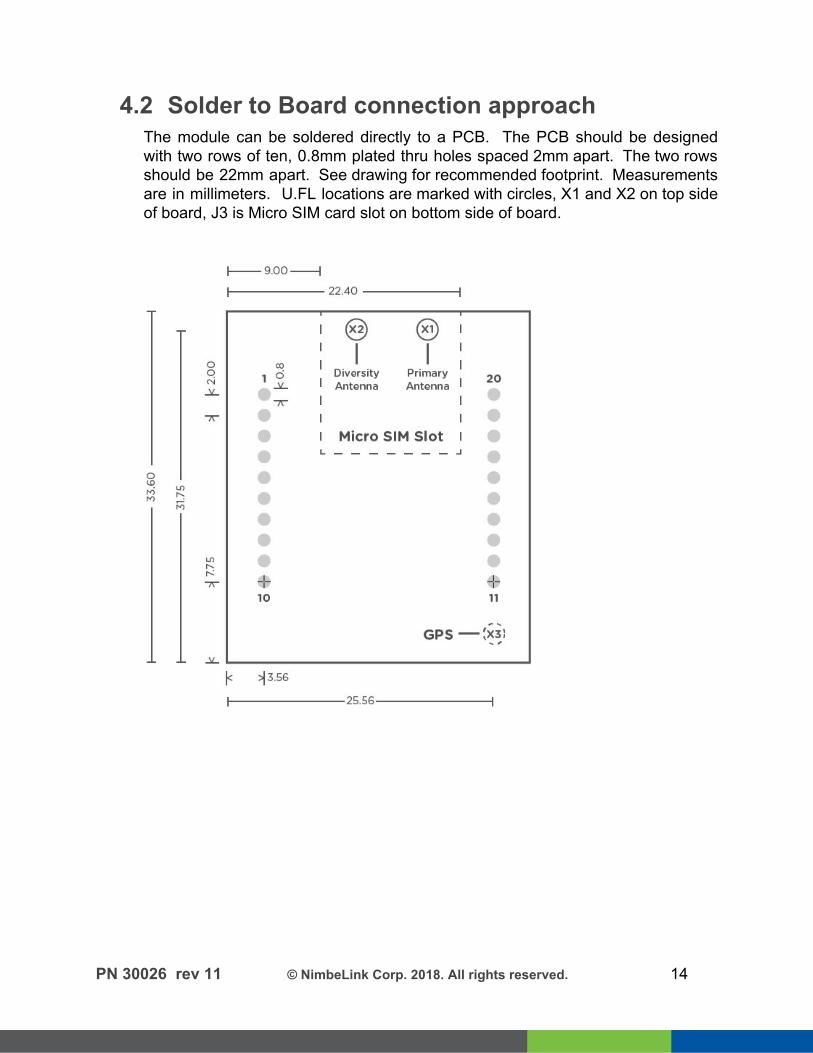
4.2 Solder to Board connection approach The module can be soldered directly to a PCB. The PCB should be designed with two rows of ten, 0.8mm plated thru holes spaced 2mm apart. The two rows should be 22mm apart. See drawing for recommended footprint. Measurements are in millimeters. U.FL locations are marked with circles, X1 and X2 on top side of board, J3 is Micro SIM card slot on bottom side of board.
PN 30026 rev 11 © NimbeLink Corp. 2018. All rights reserved. 14
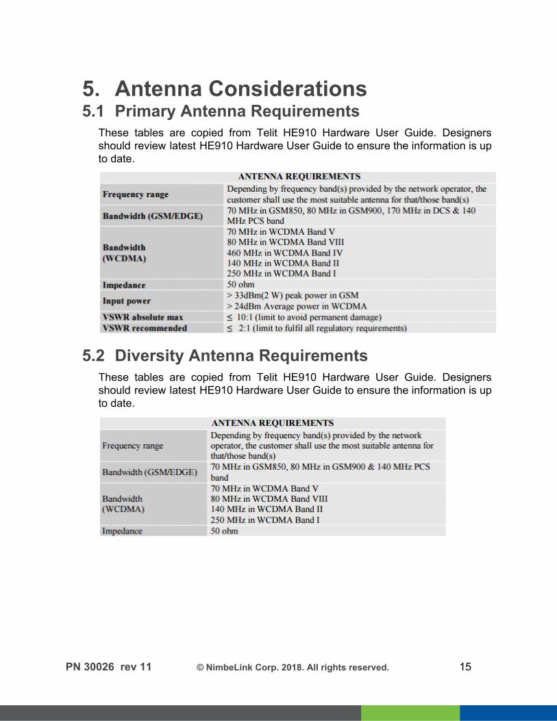
5. Antenna Considerations 5.1 Primary Antenna Requirements
These tables are copied from Telit HE910 Hardware User Guide. Designers should review latest HE910 Hardware User Guide to ensure the information is up to date.
5.2 Diversity Antenna Requirements These tables are copied from Telit HE910 Hardware User Guide. Designers should review latest HE910 Hardware User Guide to ensure the information is up to date.
PN 30026 rev 11 © NimbeLink Corp. 2018. All rights reserved. 15
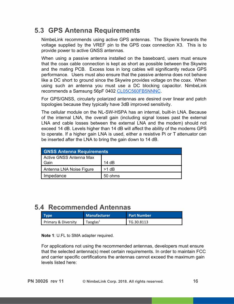
5.3 GPS Antenna Requirements NimbeLink recommends using active GPS antennas. The Skywire forwards the voltage supplied by the VREF pin to the GPS coax connection X3. This is to provide power to active GNSS antennas. When using a passive antenna installed on the baseboard, users must ensure that the coax cable connection is kept as short as possible between the Skywire and the mating PCB. Excess loss in long cables will significantly reduce GPS performance. Users must also ensure that the passive antenna does not behave like a DC short to ground since the Skywire provides voltage on the coax. When using such an antenna you must use a DC blocking capacitor. NimbeLink recommends a Samsung 56pF 0402 CL05C560FB5NNNC. For GPS/GNSS, circularly polarized antennas are desired over linear and patch topologies because they typically have 3dB improved sensitivity. The cellular module on the NL-SW-HSPA has an internal, built-in LNA. Because of the internal LNA, the overall gain (including signal losses past the external LNA and cable losses between the external LNA and the modem) should not exceed 14 dB. Levels higher than 14 dB will affect the ability of the modems GPS to operate. If a higher gain LNA is used, either a resistive Pi or T attenuator can be inserted after the LNA to bring the gain down to 14 dB. GNSS Antenna Requirements Active GNSS Antenna Max Gain 14 dB Antenna LNA Noise Figure >1 dB Impedance 50 ohms
5.4 Recommended Antennas
Type Manufacturer Part Number Primary & Diversity Taoglas1 TG.30.8113
Note 1: U.FL to SMA adapter required.
For applications not using the recommended antennas, developers must ensure that the selected antenna(s) meet certain requirements. In order to maintain FCC and carrier specific certifications the antennas cannot exceed the maximum gain levels listed here:
PN 30026 rev 11 © NimbeLink Corp. 2018. All rights reserved. 16
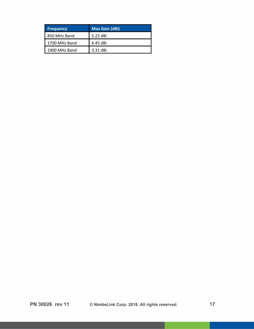
Frequency Max Gain (dBi)
850 MHz Band 5.22 dBi
1700 MHz Band 6.45 dBi
1900 MHz Band 3.31 dBi
PN 30026 rev 11 © NimbeLink Corp. 2018. All rights reserved. 17

6. Certifications 6.1 Carrier Specific
PTCRB, AT&T Rogers Each carrier has different requirements for activating the HE910 modem on their networks. Many accept the Telit PTCRB & GCF certification to allow device on the network, however, recent carrier preferences may require the end product to go through PTCRB & GCF certification in the final enclosure, antenna, and software configuration.
6.2 Geography Specific Federal Communications Commission (FCC47) part 22, 24 Complies with FCC47 Part 15 Class B Radiated and Conducted Emissions
7. Federal Regulatory Licensing 7.1 Export Control Classification Number (ECCN)
ECCNs are five character alpha-numeric designations used on the Commerce Control List (CCL) to identify dual-use items for export control purposes. An ECCN categorizes items based on the nature of the product, i.e. type of commodity, software, or technology and its respective technical parameters. All Skywire Modems: 5A992.c
7.2 Harmonized Tariff Schedule Code HTS Code: 8517.62.0010
8. End Product Labeling Requirements Device Uses Approved Radio: NL-SW-HSPA Contains FCC ID: RI7HE910 and IC ID: 5131A-HE910 This device complies with Part 15 of the FCC Rules. Operation is subject to the following two conditions: (1) This device may not cause harmful interferences, and (2) this device must accept any interference received, including interference that may cause undesired operation.
PN 30026 rev 11 © NimbeLink Corp. 2018. All rights reserved. 18