skiroc 2 & fev status
TRANSCRIPT
CSNSM
SKIROC 2 & FEV Status
Stéphane Callier, Dominique Cuisy, Julien Fleury
23 February, 2009

ASIC S h d lASIC ScheduleSKIROC 2SKIROC 2
23 February, 2009 CALICE E-cal session - Daegu, 19/02/2009 2
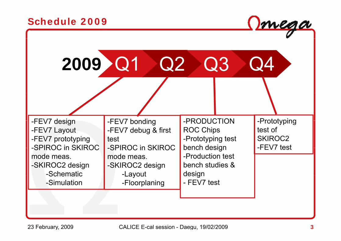
Schedule 2009
Q1 Q2 Q3 Q42009 Q1 Q2 Q3 Q42009
FEV7 design FEV7 bonding PRODUCTION Prototyping-FEV7 design-FEV7 Layout-FEV7 prototyping-SPIROC in SKIROC
-FEV7 bonding-FEV7 debug & first testSPIROC in SKIROC
-PRODUCTION ROC Chips-Prototyping test bench design
-Prototyping test of SKIROC2-FEV7 test-SPIROC in SKIROC
mode meas.-SKIROC2 design
-Schematic
-SPIROC in SKIROC mode meas.-SKIROC2 design
-Layout
bench design-Production test bench studies & design
-FEV7 test
Schematic-Simulation
Layout-Floorplaning
design- FEV7 test
23 February, 2009 CALICE E-cal session - Daegu, 19/02/2009 3

Schedule 2010
Q1 Q2 Q3 Q42010 Q1 Q2 Q3 Q42010
FEV8 design SKIROC2 SKIROC2 FEV8-FEV8 design-FEV8 Layout-FEV8 prototyping-SKIROC2 meas
-SKIROC2 production test
-SKIROC2 assembling on FEV8-FEV8 test
-FEV8 production-FEV8 prod assembling-SKIROC2 meas.
-Testbench designassembling-FEV8 prod test
23 February, 2009 CALICE E-cal session - Daegu, 19/02/2009 4

Funding request
2009 Prototyping
PCB R&D and fabricationPrototyping of FEV7 in 3 different companies to ensure (?) success of fab-Prototyping of FEV7 in 3 different companies to ensure (?) success of fab.
PCB assembly (prototype)-SKIROC2 characterization test (dicing, packaging, testboard, etc.)SKIROC2 characterization test (dicing, packaging, testboard, etc.)
Needed before assembly -SPIROC assembling on FEV7, process validation, machining
Can be done by CERN to save money, official agreement needed
2010 Production (~10 ASIC wafers)
• Microprobe station for SKIROC2 production test (100k€)• Bonding of FEV8 production (try to establish collaboration with CERN)• Selective dicing of wafers after probe testing (SKIROC)Selective dicing of wafers after probe testing (SKIROC).
SPIROC and HARDROC go to packaging• SLAB test setup in LAL to validate assembling
23 February, 2009 CALICE E-cal session - Daegu, 19/02/2009 5

SKIROC 2 block scheme proposal
1MΩ
20MΩ
Analog Memory
Gain selection Slow shaper
Gain 1
Tp=180ns
0.5 pF
g y
Depth = 15
bit A
DC
lkin
son)
ChargeM
8.5 pF
Preamp.Input
2/3pF
Calib
12-b
(Wil Meas.
fast shaper
Gain 16
Tp=15nsCalib.Input
Trigger out
Tp 15ns
4-bit DACHigh gain : 0 5 100 MIP adjustment TimeMeasurement ?
Everything in hand
High gain : 0.5 100 MIPLow gain : 100 3000 MIP
23 February, 2009 CALICE E-cal session - Daegu, 19/02/2009 6
10-bit dual DAC – common to 64 channelsy g
(from spiroc)

PCB d iPCB designFEV statusFEV status
23 February, 2009 CALICE E-cal session - Daegu, 19/02/2009 7

Reminder : FEV5 design
FEV5 manifacturing order:
• in France by LAL
• in Korea by Sungkyun Kwan University & Korea Institute of Radiological & Medical Sciences
HARDROC
PCBWAFER
18cm
WAFER
23 February, 2009 CALICE E-cal session - Daegu, 19/02/2009 8
1296 channels. 8 HARDROC (512 channels equipped)

Chip Embedding + PCB Pile-up
Pile-up
3 drilling sequences :FEV 5
Pile-upTOP GND+routingC2 AVDD+routingC3 AVDD+DVDDC4 GND + horizontal routing 3 drilling sequences :
- Laser C7-C8 120µ filled- Laser C6-C7 120µ
Mechanical C1 C7
FEV 5C4 GND + horizontal routingC5 AVDD+ vertical routingC6 GND+pads routingC7 GND (pads shielding)BOT PADS - Mechanical C1-C7BOT PADS
PCB thickness ~ 1mm
23 February, 2009 CALICE E-cal session - Daegu, 19/02/2009 9

Pile-up
Chip Embedding + PCB Pile-up
Pile-upTOP Mechanical filling layerC2 AVDD + routingC3 AVDD + DVDDC4 GND + horizontal routing FEV 7 3 drilling sequences :
TOP Mechanical filling layer
C4 GND + horizontal routingC5 AVDD+ vertical routingC6 GND + pads routingC7 GND (pads shielding)BOT PADS
FEV 7 3 drilling sequences :- Laser C7-C8 120µ filled- Laser C6-C7 120µ- Mechanical C2-C7BOT PADS - Mechanical C2-C7
Thinner PCBThinner PCBonly ~800µm
23 February, 2009 CALICE E-cal session - Daegu, 19/02/2009 10

Issues : Layer 2 not bondable
Gold?
Nickel?
CopperCopper
23 February, 2009 CALICE E-cal session - Daegu, 19/02/2009 11
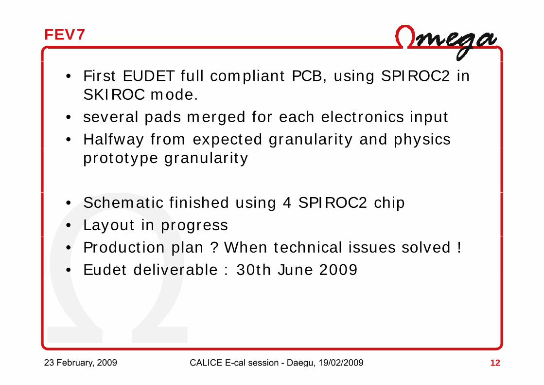
FEV7
• First EUDET full compliant PCB, using SPIROC2 in SKIROC mode.
• several pads merged for each electronics input• Halfway from expected granularity and physics
prototype granularity
• Schematic finished using 4 SPIROC2 chip• Layout in progress• Production plan ? When technical issues solved !• Eudet deliverable : 30th June 2009
23 February, 2009 CALICE E-cal session - Daegu, 19/02/2009 12
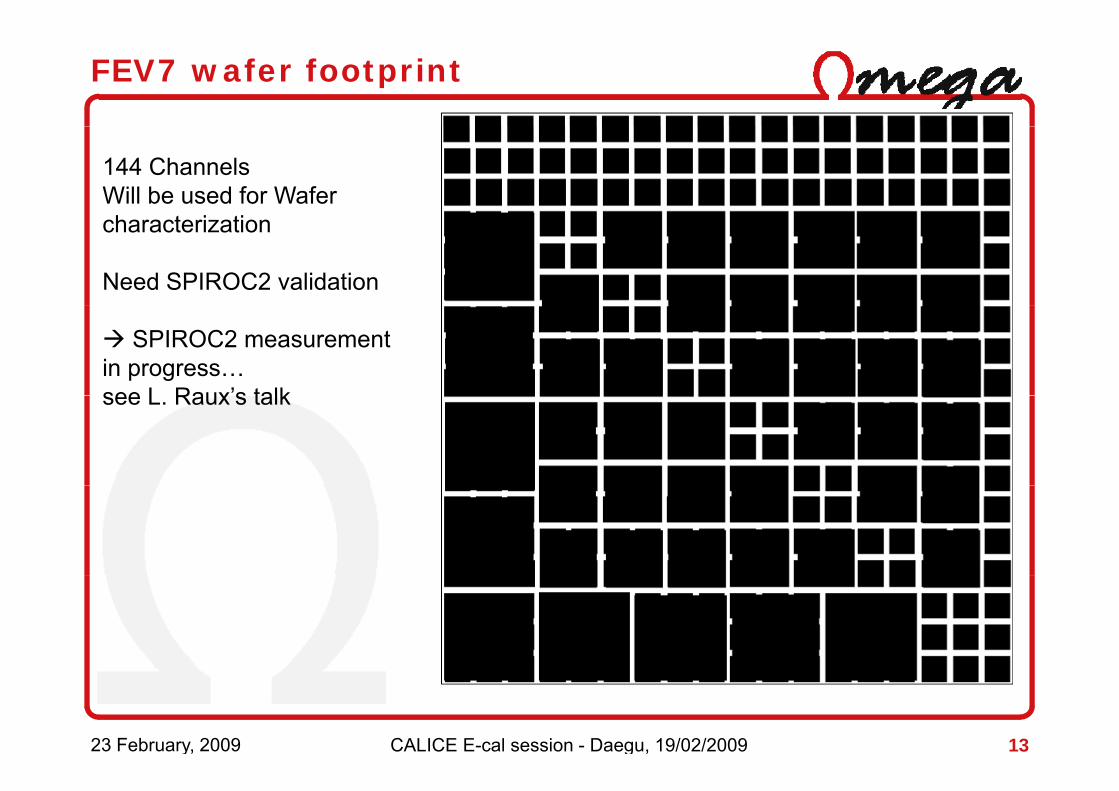
FEV7 wafer footprint
144 ChannelsWill be used for Wafer h t i ticharacterization
Need SPIROC2 validation
SPIROC2 measurementin progress… see L Raux’s talksee L. Raux s talk
23 February, 2009 CALICE E-cal session - Daegu, 19/02/2009 13

Conclusion
• PCB design– Several FEV5 engineering done, in France and in Korea…– NOT SO EASY TO BUILD still not validated since
November 2007– FEV7 design using Hamamatsu Wafer and Spiroc2– FEV7 design using Hamamatsu Wafer and Spiroc2– FEV8 plan to use skiroc2
• Opportunity to have 256 ch. Wafers ? (5.5mm pads)• Wafer size : 90 x 90 mm 16 x 16 pixels
• Front end ASIC design• Front-end ASIC design– Skiroc2 planned for June 2009– Hardroc2, Spiroc2 & Skiroc2 productionHardroc2, Spiroc2 & Skiroc2 production– Very Aggressive schedule– Funding needed for production test in 2010 !
23 February, 2009 CALICE E-cal session - Daegu, 19/02/2009 14

Backup slide : Schedule & Info
• Skiroc 2 expected to be sent in fab in June 2009– Still in design and simulation phase– Sharing of the HARDROC2 and SPIROC2 production– If SKIROC 2 is validated production in hand for EUDET
modulemodule– Cheaper than an engineering run for prototyping due to big
silicon area (60mm² ie ~60k€)
• Next PCB prototype will use SPIROC2 with H t fHamamatsu wafers– Validation of all electronics and assembling process – missing : dynamic range (500MIP/2500MIP) granularity– missing : dynamic range (500MIP/2500MIP), granularity– PCB in hand in April 2009 ?
23 February, 2009 CALICE E-cal session - Daegu, 19/02/2009 15

Backup slide : Expectations for EUDET module
• 64 channels to read out new 256 pads wafers with 4 chips– This is a critical PCB requirement– This will make SKIROC2 the biggest chip of the ROC family
• 50 60 mm²• 50-60 mm²
• Capability to operate in ILC mode and in test beam– This is a physics requirement to take data with EUDETThis is a physics requirement to take data with EUDET
module– Calculation of data rates to be validated
• High dynamic range from 0.1 to 3000 MIP• (Eventually) time measurement to tag events in
test beam (not useful in ILC mode)
23 February, 2009 CALICE E-cal session - Daegu, 19/02/2009 16