sir endec for irda applications integrated interface circuit sheets/vishay semiconductors... ·...
TRANSCRIPT

SIR Endec for IrDA® Applications Integrated Interface Circuit
TOIM4232Vishay Semiconductors
Document Number: 82546 For technical questions within your region, please contact one of the following:[email protected], [email protected], [email protected]
www.vishay.comRev. 2.1, 17-Nov-10 1
DESCRIPTION The TOIM4232 Endec IC provides proper pulse shaping forthe SIR IrDA® front end infrared transceivers as of the4000-series. For transmitting the TOIM4232 shortens theRS232 output signal to IrDA compatible electrical pulses todrive the infrared transmitter. In the receive mode, theTOIM4232 stretches the received infrared pulses to theproper bit width depending on the operating bit rate. The IrDAbit rate varies from 2.4 kbit/s to 115.2 kbit/s.The TOIM4232is using a crystal clock 3.6864 MHz for its pulse stretchingand shortening. The clock can be generated by the internaloscillator. An external clock can be used, too. The TOIM4232is programmable to operate from 1200 bit/s to 115.2 kbit/s bythe communication software through the RS232 port. Theoutput pulses are software programmable as either 1.627 µsor 3/16 of bit time. The typical power consumption is very lowwith about 10 mW in operational state and in the order of afew microwatts in standby mode.
ULC TECHNOLOGYHigh performance gate array package using multiple metallayer CMOS technology featuring sub-micron channellengths (0.35 µm).
FEATURES• Pulse shaping function (shortening and
stretching) used in SIR IrDA applications
• Directly interfaces the SIR transceiver TFD..-and TFB..- series to an RS232 port
• Programmable baud clock generator (1200 Hz to115.2 kHz), 13 baud rates
• 3/16 bit pulse duration or 1.627 µs pulseselectable
• SO16 - package
• 2.7 V to 3.6 V operation voltage, 5 V tolerant inputs
• Low operating current
• Qualified for lead (Pb)-free and Sn/Pb processing (MSL3)
• Compliant to RoHS Directive 2002/95/EC and inaccordance to WEEE 2002/96/EC
18080
PARTS TABLEPART DESCRIPTION QTY/REEL
TOIM4232-TR3 - 1500 pcs
PRODUCT SUMMARY
PART NUMBERDATA RATE
(kbit/s)
DIMENSIONSH x L x W
(mm x mm x mm)
LINK DISTANCE(m)
OPERATING VOLTAGE
(V)
IDLE SUPPLY CURRENT
(mA)
TOIM4232 115.2 4 x 4 x 0.75 - 2.7 to 3.6 2
TOIM4232Vishay Semiconductors SIR Endec for IrDA® Applications
Integrated Interface Circuit
www.vishay.com For technical questions within your region, please contact one of the following:[email protected], [email protected], [email protected]
Document Number: 825462 Rev. 2.1, 17-Nov-10
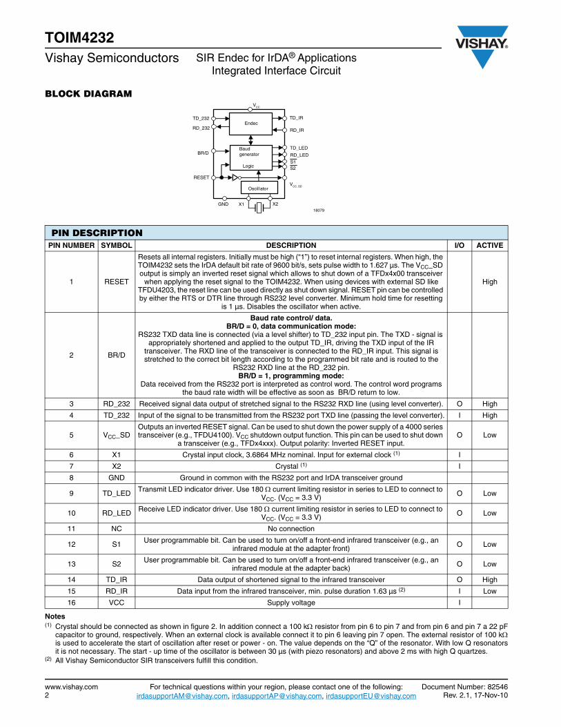
BLOCK DIAGRAM
Notes(1) Crystal should be connected as shown in figure 2. In addition connect a 100 k resistor from pin 6 to pin 7 and from pin 6 and pin 7 a 22 pF
capacitor to ground, respectively. When an external clock is available connect it to pin 6 leaving pin 7 open. The external resistor of 100 kis used to accelerate the start of oscillation after reset or power - on. The value depends on the “Q” of the resonator. With low Q resonatorsit is not necessary. The start - up time of the oscillator is between 30 µs (with piezo resonators) and above 2 ms with high Q quartzes.
(2) All Vishay Semiconductor SIR transceivers fulfill this condition.
PIN DESCRIPTIONPIN NUMBER SYMBOL DESCRIPTION I/O ACTIVE
1 RESET
Resets all internal registers. Initially must be high (“1”) to reset internal registers. When high, the TOIM4232 sets the IrDA default bit rate of 9600 bit/s, sets pulse width to 1.627 µs. The VCC_SD output is simply an inverted reset signal which allows to shut down of a TFDx4x00 transceiver
when applying the reset signal to the TOIM4232. When using devices with external SD like TFDU4203, the reset line can be used directly as shut down signal. RESET pin can be controlled by either the RTS or DTR line through RS232 level converter. Minimum hold time for resetting
is 1 µs. Disables the oscillator when active.
High
2 BR/D
Baud rate control/ data.BR/D = 0, data communication mode:
RS232 TXD data line is connected (via a level shifter) to TD_232 input pin. The TXD - signal is appropriately shortened and applied to the output TD_IR, driving the TXD input of the IR
transceiver. The RXD line of the transceiver is connected to the RD_IR input. This signal is stretched to the correct bit length according to the programmed bit rate and is routed to the
RS232 RXD line at the RD_232 pin. BR/D = 1, programming mode:
Data received from the RS232 port is interpreted as control word. The control word programs the baud rate width will be effective as soon as BR/D return to low.
3 RD_232 Received signal data output of stretched signal to the RS232 RXD line (using level converter). O High
4 TD_232 Input of the signal to be transmitted from the RS232 port TXD line (passing the level converter). I High
5 VCC_SDOutputs an inverted RESET signal. Can be used to shut down the power supply of a 4000 series transceiver (e.g., TFDU4100). VCC shutdown output function. This pin can be used to shut down
a transceiver (e.g., TFDx4xxx). Output polarity: Inverted RESET input.O Low
6 X1 Crystal input clock, 3.6864 MHz nominal. Input for external clock (1) I
7 X2 Crystal (1) I
8 GND Ground in common with the RS232 port and IrDA transceiver ground
9 TD_LED Transmit LED indicator driver. Use 180 current limiting resistor in series to LED to connect to VCC. (VCC = 3.3 V) O Low
10 RD_LED Receive LED indicator driver. Use 180 current limiting resistor in series to LED to connect to VCC. (VCC = 3.3 V) O Low
11 NC No connection
12 S1 User programmable bit. Can be used to turn on/off a front-end infrared transceiver (e.g., an infrared module at the adapter front) O Low
13 S2 User programmable bit. Can be used to turn on/off a front-end infrared transceiver (e.g., an infrared module at the adapter back) O Low
14 TD_IR Data output of shortened signal to the infrared transceiver O High
15 RD_IR Data input from the infrared transceiver, min. pulse duration 1.63 µs (2) I Low
16 VCC Supply voltage I
TD_232
RD_232
BR/D
RESET
TD_IR
RD_IR
TD_LED
RD_LED
VCC_SD
S2S1
GND X1 X2
VCC
Oscillator
Endec
Baudgenerator
Logic
18079
TOIM4232SIR Endec for IrDA® Applications
Integrated Interface CircuitVishay Semiconductors
Document Number: 82546 For technical questions within your region, please contact one of the following:[email protected], [email protected], [email protected]
www.vishay.comRev. 2.1, 17-Nov-10 3
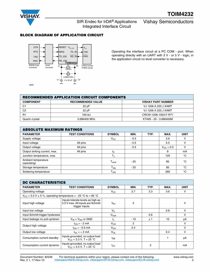
BLOCK DIAGRAM OF APPLICATION CIRCUIT
Operating the interface circuit at a PC COM - port. Whenoperating directly with an UART with 3 V - or 5 V - logic, inthe application circuit no level converter is necessary.
18081
DT R
RT S
TXD
RXD
RESET VCC_SD
BR/D TD_IR
TD_232 RD_IR
RD_232 TOIM4232
VCC
TXD
RXD
RS23 2 9 pin connector
Level converter
X1 X2 TFDU4-seriesTFBS4-series
R1
10 0 k Ω
C1 C2 3.6864 MHz
2 x 22 pF
RECOMMENDED APPLICATION CIRCUIT COMPONENTS COMPONENT RECOMMENDED VALUE VISHAY PART NUMBER
C1 22 pF VJ 1206 A 220 J XAMT
C2 22 pF VJ 1206 A 220 J XAMT
R1 100 k CRCW-1206-1003-F-RT1
Quartz crystal 3.686400 MHz XT49S - 20 - 3.686400M
ABSOLUTE MAXIMUM RATINGSPARAMETER TEST CONDITIONS SYMBOL MIN. TYP. MAX. UNIT
Supply voltage VCC - 0.5 3.6 V
Input voltage All pins - 0.5 5.5 V
Output voltage All pins - 0.5 VCC + 0.5 V
Output sinking current, max. All pins IO 8 mA
Junction temperature, max. TJ 125 °C
Ambient temperature (operating) Tamb - 25 85 °C
Storage temperature Tstg - 25 85 °C
Soldering temperature Tsldr 260 °C
DC CHARACTERISTICSPARAMETER TEST CONDITIONS SYMBOL MIN. TYP. MAX. UNIT
Operating voltage VCC 2.7 3.3 3.6 V
VCC = 3.3 V ± 5 %, operating temperature = - 25 °C to + 85 °C
Input high voltageInputs tolerate levels as high as 5.5 V max. All inputs are Schmitt
trigger inputsVIH 2 V
Input low voltage VIL 0.8 V
Input Schmitt trigger hysteresis Vhyst 0.6 V
Input leakage no pull-up/down VIN = VDD or GND IL - 10 ± 1 10 µA
Output high voltageIOH = - 2 mA VOH 2 V
IOH = - 0.5 mA VOH 2.4 V
Output low voltage IOL = + 2 mA VOL 0.4 V
Consumption current standby Inputs grounded, no output load VCC = 3.3 V, T = 25 °C ISB 1 µA
Consumption current dynamic Inputs grounded, no output load VCC = 3.3 V, T = 25 °C ICC 2 mA

TOIM4232Vishay Semiconductors SIR Endec for IrDA® Applications
Integrated Interface Circuit
www.vishay.com For technical questions within your region, please contact one of the following:[email protected], [email protected], [email protected]
Document Number: 825464 Rev. 2.1, 17-Nov-10
OPERATION DESCRIPTIONThe block diagram shows a typical example of an RS232 portinterface. The TOIM4232 connects to an RS232 levelconverter on one side, and an infrared transceiver on theother. The internal TOIM4232 baud rate generator can besoftware controlled.When BR/D = 0, the TOIM4232 interprets the channelsTD_232 to TD_IR and RD_IR to RD_232 as data channels.On the other hand, whenever BR/D = 1, the TOIM4232interprets TD_232 as control word for setting the Baud rate.The Baud rate can be programmed to operate from 1200bit/s to 115.2 kbit/s. As RS232 level converter, EIA232 orMAX232 or equivalent are recommended.When using the TOIM4232 directly connected to an UART itis compatible to 5 V TTL and 3.3 V CMOS logic.Typical external resistors and capacitors are needed asshown in the TFDU4.../TFBS4...-series references.The output pulse duration can also be programmed, seechapter “Operation Description”. It is strongly recommendedusing 1.627 µs output pulses to save battery power. Asfrequency determining component a Vishay XT49M crystal isrecommended, when no external clock is available.
We strongly recommend not to use this 3/16 modebecause 3/16 pulse length at lower bit rates consumesmore power than the shorter pulse. At a data rate of9600 bit/s, the ratio of power consumption of bothmodes is a factor of 12 (!).
PROGRAMMING THE TOIM4232For correct, data rate dependent timing the TOIM4232 isusing a built-in baud rate generator. This is used when noexternal clock is not available as in RS232 IR-dongleapplications. For programming the BR/D pin has to be setactive, BR/D = 1.In this case the TOIM4232 interprets the 7 LSBs at theTD_232 input as a control word. The operating baud rate willchange to its supposedly new baud rate when the BR/Dreturns back to low (“0”) Set the UART to 8 bit, no parity, 1stop bit.
X: do not careS1, S2: user programmable bit to program the outputs S1and S2S0: IrDA pulse selectS0 = (1): 1.627 µs pulsesS0 = (0): 3/16 bit time pulses, not recommendedB0 .. B3: baud rate select words
Example: To set TOIM4232 at COM2 port (2F8) to 9600 bit/s with 3/16bit time pulse duration send to the TOIM4232 inprogramming mode in e.g. “basic”OUT &H2F8, (&H6)For same port, 9600 bit/s and 1.627 µs pulse duration send OUT &H2F8, (&H16)For additionally activating S1 send OUT &H2F8, (&H36)
NoteIrDA standard only supports 2.4 kbit/s, 9.6 kbit/s, 19.2 kbit/s,57.6 kbit/s, and 115.2 kbit/s.
CONTROL BYTE (8 BIT)FIRST CHARACTER SECOND CHARACTER
X S2 S1 S0 B3 B2 B1 B0
LSB
TABLE 2 - BAUD RATE SELECT WORDS
B3 B2 B1 B02ND
CHARBAUD RATE
0
0 0 0 0 115.2 kHz
0 0 1 1 57.6 kHz
0 1 0 2 38.4 kHz
0 1 1 3 19.2 kHz
1 0 0 4 14.4 kHz
1 0 1 5 12.8 kHz
1 1 0 6 9.6 kHz
1 1 1 7 7.2 kHz
1
0 0 0 8 4.8 kHz
0 0 1 9 3.6 kHz
0 1 0 A 2.4 kHz
0 1 1 B 1.8 kHz
1 0 0 C 1.2 kHz
1 0 1 D forbidden
1 1 0 E forbidden
1 1 1 F forbidden

TOIM4232SIR Endec for IrDA® Applications
Integrated Interface CircuitVishay Semiconductors
Document Number: 82546 For technical questions within your region, please contact one of the following:[email protected], [email protected], [email protected]
www.vishay.comRev. 2.1, 17-Nov-10 5
SOFTWARE FOR THE TOIM4232UART PROGRAMMINGFor proper operation, the RS232 must be programmed (using 8 bit, 1 stop, no parity) to send a two character control word, YZ.The control word YZ is composed of two characters, written in hexadecimal, in format: YZ. The transfer rate for programmingmust be identical with the formerly programmed data rate, or after resetting the TOIM4232, the default rate of 9600 bit/s is used.
Note(1) For programming the UART, refer to e.g., National Semiconductor’s data sheet of PC 16550 UART
RECOMMENDED APPLICATION CIRCUIT WITH LEVEL SHIFTER
STEP. RESET BR/D TD_UART RD_UART RD_IR TD_IR DESCRIPTION AND COMMENTS
1 High X X X X X Resets all internal registers. Resets to IrDA default data rate of 9600 bit/s
2 Low X X X X XWait at least 2 ms, to allow start-up of internal clock. When external clock is
used: wait at least 7 µs.
3 Low High X X X X Wait at least 7 µs. TOIM4232 now is set to the control word programming mode
4 Low High
YZ with Y = 1for 1.627 µs
Y = 03/16 bit length
X X X
Sending the control word YZ.Examples: send “1Z” if 1.627 µs pulses
are intended to be used. Otherwise send “0Z” for 3/16 bit period pulses. “Y6” keeps the 9.6 kbit/s data rate.
Z = 0 sets to 115.2 kbit/s, see programming table.
Wait at least 1 µs for hold-time.
5 Low Low Data Data Data Data
With BR/D = 0, TOIM4232 is in the data communication mode. Both RESET
and BR/D must be kept low (“0”) during data transmission. Reprogramming to a
new data rate can be resumed by restarting from step 3. The UART itself also must set to the correct data rate (1).
RXD
DTR (RESET)TXD
RTS (BR/D)
VCC
U4
TFDU4101TFDU4300
2
4
6
8 7
5
3
1IRED Cathode
RXD
VCC1
GND TFDU4101: NCTFDU4300: Vlog
SD
TXD
IREDAnode
J1
CON9
1
2
3
4
5
6
7
8
9
+C3
+C4
+ C5
+
C6
U2
TOIM4232TOIM5232
1
2
3
4
5
6
7
8 9
15
14
13
12
11
10
16RESET
BR/D
RD_232
TD_232
VCC_SDX1
X2
GND TD_LED
RD_IR
TD_IR
S2
S1
NC
RD_LED
VCC
+ C7
U1
MAX3232CSE
138
1110
1
3
4
5
2
6
129
147
16
15
R1INR2IN
T1INT2IN
C1+
C1-
C2+
C2-
V+
V-
R1OUTR2OUT
T1OUTT2OUT
VCC
GND
R2
C9C8
Z2
R1 Y1
C1 + C2J2
CON2
12
R4R3
+C10
C11
External input3.6 V max.
optional
This line not used with TFDU4101
20612
TOIM4232Vishay Semiconductors SIR Endec for IrDA® Applications
Integrated Interface Circuit
www.vishay.com For technical questions within your region, please contact one of the following:[email protected], [email protected], [email protected]
Document Number: 825466 Rev. 2.1, 17-Nov-10
RECOMMENDED APPLICATION CIRCUIT COMPONENTS COMPONENT RECOMMENDED VALUE VISHAY PART NUMBER
1 C1 100 nF VJ 1206 Y 104 J XXMT
2 C2 10 µF, 16 V 293D106X9016B2T
3 C3 100 nF VJ 1206 Y 104 J XXMT
4 C4 100 nF VJ 1206 Y 104 J XXMT
5 C5 100 nF VJ 1206 Y 104 J XXMT
6 C6 100 nF VJ 1206 Y 104 J XXMT
7 C7 1 µF, 16 V 293D105X9016A2T
8 C8 22 pF VJ 1206 A 220 J XAMT
9 C9 22 pF VJ 1206 A 220 J XAMT
10 C10 6.8 µF, 16 V 293D 685X9 016B 2T
11 C11 100 nF VJ 1206 Y 104 J XXMT
12 Z2 3.6 V BZT55C3V6
13 R1 5.6 k CRCW-1206-5601-F-RT1
14 R2 Depending on resonator quality CRCW-1206-1003-F-RT1
15 R3 47 CRCW-1206-47R0-F-RT1
16 R4 For operation according IrDA - spec not needed Optional only for current reduction
17 Y1 3.686400 MHz XT49S - 20 - 3.686400M or e.g. ceramic resonators
18 U1 MAXIM MAX 3232E
19 U2 TOIM4232 or TOIM5232
20 U3 TFDU4300 or other compatible transceivers
21 J1 9 pin - D-sub Cannon
22 J2 Power connector

TOIM4232SIR Endec for IrDA® Applications
Integrated Interface CircuitVishay Semiconductors
Document Number: 82546 For technical questions within your region, please contact one of the following:[email protected], [email protected], [email protected]
www.vishay.comRev. 2.1, 17-Nov-10 7
RECOMMENDED APPLICATION CIRCUIT WITH DISCRETE LEVEL SHIFTERS
Install jumper connection only when VCC_SD supplies U2. In that case leave R11 off.
VB1
SUB-D 9
594837261
D7
3
1
+
C6
R12/1
R9
R11
RTS
IRED1
Q13
1
2
Q2
R12/2
C4
+C2 R2
R3
TXD
Q33
1
2
R10
D1
C5
R5 R1
R6
U2 TFDU4100
34
56
78
12
V
Gnd SC
TXD
IRED anodeIRED cathode
RXD
R13
Jumper
DTR
U1TOIM42321
2
3
4
5
6
7
8 9
15
14
13
12
11
10
16Reset
BR/D
RD_232
TD_232
V
X1
X2
GND TTD_LED
RD_IR
TD_IR
S2
S1
NC
RD_LED
V
C3
Q4
3
1
2
D2RXD
+C1
QZ1
D4
D3
1
TXD
RTSRXD
+ 3.3 V
VCC
NC
V+ 3.3 VResetBR/DRD232TD232
D6D5
3
2
Reset
Q1
R20
CC
CC
CC_SD
CC
18082

TOIM4232Vishay Semiconductors SIR Endec for IrDA® Applications
Integrated Interface Circuit
www.vishay.com For technical questions within your region, please contact one of the following:[email protected], [email protected], [email protected]
Document Number: 825468 Rev. 2.1, 17-Nov-10
RECOMMENDED APPLICATION CIRCUIT COMPONENTSCOMPONENT RECOMMENDED VALUE VISHAY PART NUMBER
1 C1 22 µF, 16 V 293D 226X9 016C 2T
2 C2 47 µF, 16 V 293D 476X9 016D 2T
3 C3 22 pF VJ 1206 A 220 J XAMT
4 C4 22 pF VJ 1206 A 220 J XAMT
5 C5 100 nF VJ 1206 Y 104 J XXMT
6 C6 6.8 µF, 16 V 293D 685X9 016B 2T
7 D1 1N4148
8 D2 1N4148
9 D4 BZT55C4V7
10 D5 1N4148
11 D6 1N4145
12 D7 BZT55C3V9
13 IRED1 TSHF5400
14 Jumper CRCW-1206-000-F-RT1
15 LED1 TLLY4401
16 LED2 TLLG4401
17 Q1 BC817-25
18 Q2 VP 0610 0T
19 Q3 BC817-25
20 Q4 BC817-25
21 QZ1 3.686400 MHz XT49S - 20 - 3.686400M
22 R1 22 k CRCW-1206-2202-F-RT1
23 R2 10 k CRCW-1206-1002-F-RT1
24 R3 22 k CRCW-1206-2202-F-RT1
25 R5 1 k CRCW-1206-1001-F-RT1
26 R6 47 k CRCW-1206-4702-F-RT1
27 R9 5.6 k CRCW-1206-5601-F-RT1
28 R10 100 k CRCW-1206-1003-F-RT1
29 R11 100 CRCW-1206-1000-F-RT1
30 R12 20 CRCW-1206-20R0-F-RT1
21 R13 1 k CRCW-1206-1001-F-RT1
32 R17 750 CRCW-1206-7500-F-RT1
33 R18 750 CRCW-1206-750-F-RT1
34 VB1 9 pin - D - sub Cannon
35 U1 TOIM4232 or TOIM5232
36 U2 TFDU4100 (will be obsolete). Replace by TFDU4101 and use external components as shown in the other example.
TOIM4232SIR Endec for IrDA® Applications
Integrated Interface CircuitVishay Semiconductors
Document Number: 82546 For technical questions within your region, please contact one of the following:[email protected], [email protected], [email protected]
www.vishay.comRev. 2.1, 17-Nov-10 9
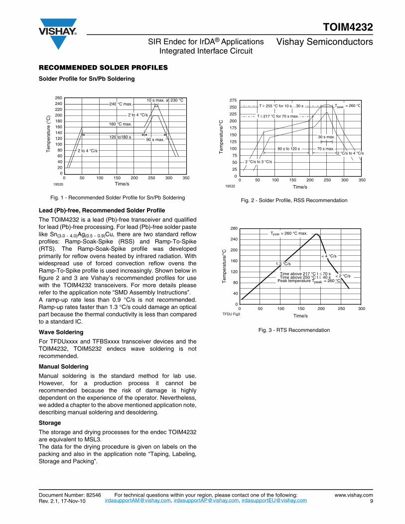
RECOMMENDED SOLDER PROFILES
Solder Profile for Sn/Pb Soldering
Fig. 1 - Recommended Solder Profile for Sn/Pb Soldering
Lead (Pb)-free, Recommended Solder Profile
The TOIM4232 is a lead (Pb)-free transceiver and qualifiedfor lead (Pb)-free processing. For lead (Pb)-free solder pastelike Sn(3.0 - 4.0)Ag(0.5 - 0.9)Cu, there are two standard reflowprofiles: Ramp-Soak-Spike (RSS) and Ramp-To-Spike(RTS). The Ramp-Soak-Spike profile was developedprimarily for reflow ovens heated by infrared radiation. Withwidespread use of forced convection reflow ovens theRamp-To-Spike profile is used increasingly. Shown below infigure 2 and 3 are Vishay’s recommended profiles for usewith the TOIM4232 transceivers. For more details pleaserefer to the application note “SMD Assembly Instructions”.A ramp-up rate less than 0.9 °C/s is not recommended.Ramp-up rates faster than 1.3 °C/s could damage an opticalpart because the thermal conductivity is less than comparedto a standard IC.
Wave Soldering
For TFDUxxxx and TFBSxxxx transceiver devices and theTOIM4232, TOIM5232 endecs wave soldering is notrecommended.
Manual Soldering
Manual soldering is the standard method for lab use.However, for a production process it cannot berecommended because the risk of damage is highlydependent on the experience of the operator. Nevertheless,we added a chapter to the above mentioned application note,describing manual soldering and desoldering.
Storage
The storage and drying processes for the endec TOIM4232are equivalent to MSL3.The data for the drying procedure is given on labels on thepacking and also in the application note “Taping, Labeling,Storage and Packing”.
Fig. 2 - Solder Profile, RSS Recommendation
Fig. 3 - RTS Recommendation
020406080
100120140160180200220240260
0 50 100 150 200 250 300 350
Time/s
Tem
pera
ture
(°C
)
2 to 4 °C/s
2 to 4 °C/s
10 s max. at 230 °C
120 to180 s
160 °C max.
240 °C max.
90 s max.
19535
0
25
50
75
100
125
150
175
200
225
250
275
0 50 100 150 200 250 300 350
Time/s
Tem
pera
ture
/°C
30 s max.
2 °C/s to 3 °C/s
2 °C/s to 4 °C/s90 s to 120 s
T ≥ 217 °C for 70 s max.
Tpeak = 260 °C
70 s max.
T ≥ 255 °C for 10 s....30 s
19532
0
40
80
120
160
200
240
280
0 50 100 150 200 250 300
Time/s
Tem
pera
ture
/°C
< 4 °C/s
1.3 °C/s
Time above 217 °C t ≤ 70 sTime above 250 °C t ≤ 40 s
Peak temperature Tpeak = 260 °C< 2 °C/s
Tpeak = 260 °C max.
TFDU Fig3

TOIM4232Vishay Semiconductors SIR Endec for IrDA® Applications
Integrated Interface Circuit
www.vishay.com For technical questions within your region, please contact one of the following:[email protected], [email protected], [email protected]
Document Number: 8254610 Rev. 2.1, 17-Nov-10
PACKAGE DIMENSIONS in millimeters
REEL DIMENSIONS in millimeters
13011
14017
Drawing-No.: 9.800-5090.01-4Issue: 1; 29.11.05
TAPE WIDTH(mm)
A MAX.(mm)
N(mm)
W1 MIN.(mm)
W2 MAX.(mm)
W3 MIN.(mm)
W3 MAX.(mm)
16 330 50 16.4 22.4 15.9 19.4

TOIM4232SIR Endec for IrDA® Applications
Integrated Interface CircuitVishay Semiconductors
Document Number: 82546 For technical questions within your region, please contact one of the following:[email protected], [email protected], [email protected]
www.vishay.comRev. 2.1, 17-Nov-10 11
TAPE DIMENSIONS in millimeters
18241

TOIM4232Vishay Semiconductors SIR Endec for IrDA® Applications
Integrated Interface Circuit
www.vishay.com For technical questions within your region, please contact one of the following:[email protected], [email protected], [email protected]
Document Number: 8254612 Rev. 2.1, 17-Nov-10
TOIM4232 (TOIM5232) ENCODER - DECODER INTERFACEPROGRAMMING AND DATA TRANSMISSIONOperation and programming of the TOIM4232 andTOIM5232 interface devices are described below. Figure 4shows the basic circuit design with 3 blocks: the RS232 to3 V logic level shifter, the encoder/decoder (endec) circuitand the transceiver to build a dongle for RS232 IrDA
extension. U1 is the level shifter to convert the RS232 logiclevels to unipolar 3 V logic; U2 is the encoder/decoderInterface (endec) converting the NRZ - RS232 logic to IrDARZI - logic. The transceiver U3 transmits and receivesIrDA-compliant optical signals.
Fig. 4 - Circuit Diagram of the Demo Board
CIRCUIT DESCRIPTIONThis circuit demonstrates the operation of an SIR IrDAtransceiver module. The transceiver U3 (e.g., as shown theTFDU4101 or TFDU4300 or any other) converts the digitalelectrical input signal to an optical output signal to betransmitted, receives the optical signal, and converts theseto electrical digital signals. While the IrDA physical layerprotocol transmits only the “0” represented by a pulse with a“Return to Zero Inverted (RZI)” logic, the RS232 protocolneeds a “No Return to Zero (NRZ)” representation. Thisdecoding/encoding process is done by U2, an interfacecircuit stretching the received pulses and shortening thepulses to be transmitted according to the IrDA physical layerconditions. U1 interfaces the RS232 logic bipolar levels tothe 3 V logic of the endec U2. The board is connected byCON9 to the RS232 port (of a computer or other equipment.The basic IrDA transmission speed is 9600 bit/s. This is thedefault state of the endec in power-on condition. Also,activating the reset line at pin 1 (18) will set the device to thisbasic state.Note: The first pin number refers to TOIM4232; the secondnumber in brackets refers to TOIM5232. The crystal Y1controls the timing of the endec as a clock reference. Theoutputs S1 and S2 are programmable outputs for controloperations and the outputs RD_LED and TD_LED can driveLEDs for indicating data flow.
PROGRAMMING THE ENDECFor decoding data rates other than the default, the endec isto be programmed to set the internal counters and timers. Toswitch the endec from the data transfer mode to the bit rateprogramming mode, the input BR/D, pin 2 (19) is set activehigh (BR/D = “1”). In this case the TOIM5232 interprets the7 LSBs at the TD_232 input as a control word. The operatingbit rate will change to its supposedly new rate when the BR/Dreturns back to low (“0”). Set the UART to 8 bit, no parity, 1stop bit.The control byte consists of 8 bit after the start bit (STA,which is “0”). Keep in mind that the order is LSB first, MSBlast.The diagram in figure 5 shows the programming byte“0-1010-1100” in the order STA, B0, B1, B2, B3, S0, S1, S2, X. This order is from rightto left in table 1. B0 is sent first as LSB (see figure 5).The four least significant bits are responsible for the data rateaccording to table 2 while the four higher bits are for settingthe IrDA pulse duration (S0), and the two outputs of theEndec S1 and S2. Bit 8 is not used.
RXD TXD
RTS (BR/D)
U3
TFDU4101
2
4
6
8 5 3 1
7
Cathode
RXD
Vcc1
GND SD
TXD Anode
.
C3
J1
CON9
1
2
3
4
5
6
7
8
9
C6 C5
U2
TOIM4232
1(18)
2(19) 3(1)
4(2)
5(3) 6(4)
7(5)
8(7) 9(9)
15(16)
14(14) 13(13) 12(12)
11 *) 10(10)
16(17) RESET
BR/D RD_232 TD_232 Vcc_SD
X1
X2
GND TD_LED
RD_IR TD_IR
S2
S1
NC
RD_LED
Vcc
C7
U1
MAX3232
13 8
11 10
1
3
4
5
2
6
12 9
14 7
16
15
R1IN R2IN
T1IN T2IN
C+
C1-
C2+
C2-
V+
V-
R1OUT R2OUT
T1OUT T2OUT
VCC
GND
C8 C9
R2 Z2
R1
+ C2 C1
Y1
J2
CON2
1 2
R4
C4
R3
C11
+ C10
External input 3.6V max.
DTR (RESET)
+
+ (TOIM5232)
TFDU4300
optional
TFDU4300:Vlog TFDU4101:NC
This line not used fot TFDU4101
IRED IRED
+ + +
Vcc
*) (6), (8), (11), (15), (20)
21046

TOIM4232SIR Endec for IrDA® Applications
Integrated Interface CircuitVishay Semiconductors
Document Number: 82546 For technical questions within your region, please contact one of the following:[email protected], [email protected], [email protected]
www.vishay.comRev. 2.1, 17-Nov-10 13
X: do not careS1, S2: user-programmable bit to program the outputs S1and S2. In the example, S1 is set active, and S2 is inactive.S0: IrDA pulse selectS0 = (1): 1.627 µs outputS0 = (0): 3/16 bit time pulses, not recommendedB0 to B3: baud rate select words according to the followingtable 2 below.
Bold: see example
Note• IrDA standard only supports 2.4 kbit/s, 9.6 kbit/s, 19.2 kbit/s,
57.6 kbit/s, and 115.2 kbit/s (3.6864 MHz clock). Doubling thebaud rates is permissible by doubling the clock frequency.
In figure 5 the programming sequence is shown for a bit rateof 12.8 kbit/s.
Fig. 5 - Programming sequence for setting the endec to a bit rate of 12.8 kbit/s. After setting BR/D high (Ch1), the programming
sequence with the control byte (Ch2) is applied to TD_232, pin 4.
Fig. 6 - Programming sequence for setting the endec to a bit rate of
12.8 kbit/s as in figure 5 but with a 3/16 bit pulse duration (S0 = “0”).
When correctly programmed, the endec shortens the pulseto be transmitted from the full bit duration to either 3/16 of thebit length or to 1.627 µs (which is 3/16 of the 115.2 kbit/s bitduration). For power saving, the short pulse isrecommended.The received optical pulse shows in case of most of theVishay SIR transceivers, constant pulse duration. The Endecstretches that to the correct bit time according the bit ratesetting. This is shown in the following chapters.
TABLE 1 - CONTROL BYTE (8 BIT)FIRST CHARACTER SECOND CHARACTER STA
X S2 S1 S0 B3 B2 B1 B0 0
MSB LSB
Example
0 0 1 1 0 1 0 1 0
In the oscilloscope that will be shown in the reserved order with LSB first, see figure 5.
STA FIRST CHARACTER SECOND CHARACTER
0 B0 B1 B2 B3 S0 S1 S2 X
LSB MSB
Example
0 1 0 1 0 1 1 0 0
TABLE 2 - TRANSMISSION RATE SELECT WORDSB3 B2 B1 B0 HEX BIT RATE
0 0 0 0 0 115.2 kHz
0 0 0 1 1 57.6 kHz
0 0 1 0 2 38.4 kHz
0 0 1 1 3 19.2 kHz
0 1 0 0 4 14.4 kHz
0 1 0 1 5 12.8 kHz
0 1 1 0 6 9.6 kHz
0 1 1 1 7 7.2 kHz
1 0 0 0 8 4.8 kHz
1 0 0 1 9 3.6 kHz
1 0 1 0 A 2.4 kHz
1 0 1 1 B 1.8 kHz
1 1 0 0 C 1.2 kHz
EXAMPLE
0 0 1 0 0 1 0 1 0
MSB LSB STA
1->
2->
21038
1) Ch1: BR/D; pin 2, vertical scale: 2 V/div., horizontal scale: 200 µs/div. 2) Ch2: TD_232; pin 4; programming sequence
1->
2->
1) Ch1: BR/D, pin 2, vertical scale: 2 V/div., horizontal scale: 200 µs/div. 2) Ch2: TD_232, pin 4; programming sequence
21030
STA 1 0 1 0 0 1 0 0

TOIM4232Vishay Semiconductors SIR Endec for IrDA® Applications
Integrated Interface Circuit
www.vishay.com For technical questions within your region, please contact one of the following:[email protected], [email protected], [email protected]
Document Number: 8254614 Rev. 2.1, 17-Nov-10
TRANSMIT (TXD) CHANNELFigure 7 shows the transmission in the default mode. Fordata transfer, the endec is set to that mode by BR/D = “0”. Inthe examples "6" is always transmitted (binary “00000110”).The “0” is represented in the IrDA protocol by an opticalpulse. Also here the LSB is transmitted first after the start bit.“1” is not transmitted.
Fig. 7 - Data Transmission with 9.6 kbit/s,1.627 µs Pulse Duration
Channel 1 shows the signal from the RS232 port alreadyconverted to 3 V logic by U1. The endec encodes that signalto the RZI IrDA format where a “0” is represented by a pulse.That is the trace of channel 2. This output is connected theTXD input of the transceiver and this signal is transmitted asoptical output signal. Channel 3 is the signal for an indicatorlamp connected to the TD_LED driver output. Use 180 serial resistor to supply voltage for limiting the currentthrough the LED (not shown in the circuit diagram).When using the (not recommended) 3/16-bit pulse width theoscillogram looks like figure 8.
Fig. 8 - Data Transmission with the Setting 9.6 kbit/s,3/16 bit Pulse Duration (19.5 µs)
The transmission with the highest SIR bit rate of 115.2 bit/slooks like what is shown in figure 9. However, the horizontaltime scale is different.
Fig. 9 - Data transmission with the setting 115.2 kbit/s, 1.627 µs pulse
duration. By definition, the pulse duration of 1.627 µs is identical to the 3/16-bit pulse width.
RECEIVE (RXD) CHANNELIn the default 9600 bit/s mode the signals will look like thoseshown in figure 10 and figure 11.
Fig. 10 - Data Reception with the Setting 9.6 kbit/s.Short RXD Pulse.
1->
T2->
3->
21031
STA 0 1 1 0 0 0 0 0
1) Ch1: TD_232 inp. pin 4, vertical scale: 2 V/div., horizontal scale: 200 µs/div.2) Ch2: TD_IR, pin 14; 1.6 µs pulse duration3) Ch3: TD_LED, pin 9
1->
2->
3->
21032
1) Ch1: TD_232, pin 4, vertical scale: 2 V/div., horizontal scale: 200 µs/div.2) Ch2: TD_IR, pin 14; 3/16 bit pulse duration 3) Ch3: TD_LED, pin 9
3->
1->
2->
21033
1) Ch1: TD_232, pin 4, vertical scale: 2 V/div., horizontal scale: 20 µs/div. 2) Ch2: TD_IR, pin 14; 1.6 µs pulse duration3) Ch3: TD_LED, pin 9
1->
2->
3->
21034
1) Ch1: TOIM4232; RD_IR, pin 15, vertical scale: 2 V/div., horizontal scale: 200 µs/div.2) Ch2: TOIM4232; RD_232, pin 33) Ch3: TOIM4232; RD_LED, pin 10
TOIM4232SIR Endec for IrDA® Applications
Integrated Interface CircuitVishay Semiconductors
Document Number: 82546 For technical questions within your region, please contact one of the following:[email protected], [email protected], [email protected]
www.vishay.comRev. 2.1, 17-Nov-10 15
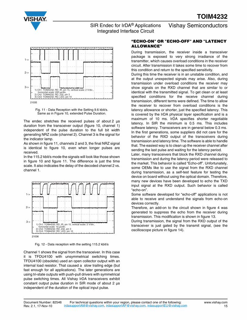
Fig. 11 - Data Reception with the Setting 9.6 kbit/s.Same as in Figure 10, extended Pulse Duration.
The endec stretches the received pulses of about 2 µsduration from the transceiver output (figure 10, channel 1)independent of the pulse duration to the full bit widthgenerating NRZ code (channel 2). Channel 3 is the signal forthe indicator lamp.As shown in figure 11, channels 2 and 3, the final NRZ signalis identical to figure 10, even when longer pulses arereceived.In the 115.2 kbit/s mode the signals will look like those shownin figure 10 and figure 11. The difference is just the timescale. It also indicates the delay of the decoded channel 2 vs.channel 1.
Fig. 12 - Data reception with the setting 115.2 kbit/s
Channel 1 shows the signal from the transceiver. In this caseit is TFDU4100 with unsymmetrical switching times.TFDU4100 (obsolete) used an open collector output with aninternal load resistor. That caused a slow trailing edge (butfast enough for all applications). The later generations areusing tri-state outputs with push-pull drivers with symmetricalpulse switching times. All Vishay IrDA transceivers exhibitconstant output pulse duration in SIR mode of about 2 µsindependent of the duration of the optical input pulse.
“ECHO-ON" OR "ECHO-OFF" AND "LATENCY ALLOWANCE”During transmission, the receiver inside a transceiverpackage is exposed to very strong irradiance of thetransmitter, which causes overload conditions in the receivercircuit. After transmission it takes some time to recover fromthis condition and return to the specified sensitivity.During this time the receiver is in an unstable condition, andat the output unexpected signals may arise. Also, duringtransmission under overload conditions the receiver mayshow signals on the RXD channel that are similar to oridentical with the transmitted signal. To get clean or at leastspecified conditions for the receive channel duringtransmission, different terms were defined. The time to allowthe receiver to recover from overload conditions is thelatency allowance or shorter, just the specified latency. Thisis covered by the IrDA physical layer specification and is amaximum of 10 ms. IrDA specifies shorter negotiablelatency. In SIR the minimum is 0.5 ms. This includessoftware latency. Transceivers are in general below 0.3 ms.In the first generations, some suppliers did not care for thebehavior of the RXD output of the transceivers duringtransmission and latency time. The software is able to handlethat. The easiest way is to clean up the receiver channel aftersending the last pulse and waiting for the latency period.Later, many transceivers that block the RXD channel duringtransmission and during the latency period were released tothe market. This behavior is called “Echo-off”. Unfortunately,some OEMs like to use the signal from the RXD channelduring transmission, as a self-test feature for testing thedevice on board without using the optical domain. Therefore,many new devices have been developed to echo the TXDinput signal at the RXD output. Such behavior is called“echo-on”.Some software developed for “echo-off” applications is notable to receive and understand the signals from echo-ondevices correctly.Therefore, an add-on to the circuit shown in figure 4 wasgenerated to suppress the echo from the receiver duringtransmission. This modification is shown in figure 13.During transmission, the signal from the RXD output of thetransceiver is just gated by the transmit signal, (see theoscilloscope picture in figure 14).
1->
2->
3->1) Ch1: TOIM4232; RD_IR, pin 15, vertical scale: 2 V/div., horizontal scale: 200 µs/div. 2) Ch2: TOIM4232; RD_232, pin 33) Ch3: TOIM4232; RD_LED, pin 10
21035
1->
2->
3->
21036
1) Ch1: TOIM4232; RD_IR, pin 15, vertical scale: 2 V/div., horizontal scale: 10 µs/div. 2) Ch2: TOIM4232; RD_232, pin 33) Ch3: TOIM4232; RD_LED, pin 10

TOIM4232Vishay Semiconductors SIR Endec for IrDA® Applications
Integrated Interface Circuit
www.vishay.com For technical questions within your region, please contact one of the following:[email protected], [email protected], [email protected]
Document Number: 8254616 Rev. 2.1, 17-Nov-10
Fig. 13 - Demo Board Circuit with Echo-Suppression to be Used for Echo-On and Echo-Off Transceivers.
Additionally, with the programmable output S1 of the endecthe echo suppression feature can be switched on and off fortesting. The default mode is echo-off. To enable the echo, S1is to be set inactive/low. (See the chapter for programmingthe TOIM4232, TOIM5232).The oscilloscope diagrams are shown in figure 14. Channel2 shows the echo signal on the RXD output of the TFDU4101transceiver during transmission (Note: TFDU4300 is anecho-off design and would not show this).Channel 1 is the signal used for gating the path from thetransceiver RXD output to the endec. On channel 3 the signalat the input of the endec is shown with a residual signal.Finally, the output to the RS232 port, RD_232, is cleanwithout any noise signal.
Fig. 14 - Echo-Suppression
TFDU4300:Vlog
Y1
C1
U2
TOIM4232*) 1 2 3 4 5 6 7 8 9
15 14 13 12 11 10
16 RESET BR/D
RD_232 TD_232 Vcc_SD X1
X2
GND TD_LED
RD_IR TD_IR
S2 S1
NC RD_LED
Vcc
R3
+ C10
TXD RXD
R5 U4
DG2039
1
4 8
3 7
2 6 5
NC_1
D V+
INS2 INS1
COM_1 COM_2 NO_2
C8
DTR (RESET)Vcc
+ C2 External input 3.6V max.
U1
MAX3232
13 8
11 10
1
3
5
2 6
12 9
14 7
16
15
R1IN R2IN
T1IN T2IN
C+
C1- C2+
C2-
V+ V-
R1OUT R2OUT
T1OUT T2OUT
VCC
optional
+
U3
TFDU4101 2
4
6
8 5 3
1
7
Cathode RXD Vcc1 GND
SD TXD
Anode
.
This line not used forTFDU4101
C6 +
R2
C3
J2
CON2
1 2
Z2
C7
+
+
C11
J1
CON9
1 2 3 4 5
6 7 8 9
Pin7: TFDU4101:NC
RTS (BR/D)
TFDU4300
C5 C4
C9
Z1
R1
+
R4
*) For TOIM5232 pinning, see figure 1.
21047
1->
2->
3->
4->
21037
1) Ch1: TOIM4232; TD_232, pin 4, vertical scale: 2 V/div., horizontal scale: 20 µs/div.2) Ch2: TFDU4101; RXD, pin 4 (IR)3) Ch3: TOIM4232; RD_IR, pin 154) Ch4: TOIM4232; RD_232, pin 3

Document Number: 91000 www.vishay.comRevision: 11-Mar-11 1
Disclaimer
Legal Disclaimer NoticeVishay
ALL PRODUCT, PRODUCT SPECIFICATIONS AND DATA ARE SUBJECT TO CHANGE WITHOUT NOTICE TO IMPROVERELIABILITY, FUNCTION OR DESIGN OR OTHERWISE.
Vishay Intertechnology, Inc., its affiliates, agents, and employees, and all persons acting on its or their behalf (collectively,“Vishay”), disclaim any and all liability for any errors, inaccuracies or incompleteness contained in any datasheet or in any otherdisclosure relating to any product.
Vishay makes no warranty, representation or guarantee regarding the suitability of the products for any particular purpose orthe continuing production of any product. To the maximum extent permitted by applicable law, Vishay disclaims (i) any and allliability arising out of the application or use of any product, (ii) any and all liability, including without limitation special,consequential or incidental damages, and (iii) any and all implied warranties, including warranties of fitness for particularpurpose, non-infringement and merchantability.
Statements regarding the suitability of products for certain types of applications are based on Vishay’s knowledge of typicalrequirements that are often placed on Vishay products in generic applications. Such statements are not binding statementsabout the suitability of products for a particular application. It is the customer’s responsibility to validate that a particularproduct with the properties described in the product specification is suitable for use in a particular application. Parametersprovided in datasheets and/or specifications may vary in different applications and performance may vary over time. Alloperating parameters, including typical parameters, must be validated for each customer application by the customer’stechnical experts. Product specifications do not expand or otherwise modify Vishay’s terms and conditions of purchase,including but not limited to the warranty expressed therein.
Except as expressly indicated in writing, Vishay products are not designed for use in medical, life-saving, or life-sustainingapplications or for any other application in which the failure of the Vishay product could result in personal injury or death.Customers using or selling Vishay products not expressly indicated for use in such applications do so at their own risk and agreeto fully indemnify and hold Vishay and its distributors harmless from and against any and all claims, liabilities, expenses anddamages arising or resulting in connection with such use or sale, including attorneys fees, even if such claim alleges that Vishayor its distributor was negligent regarding the design or manufacture of the part. Please contact authorized Vishay personnel toobtain written terms and conditions regarding products designed for such applications.
No license, express or implied, by estoppel or otherwise, to any intellectual property rights is granted by this document or byany conduct of Vishay. Product names and markings noted herein may be trademarks of their respective owners.