sipm readout electronics overview · content • sipm electrical modelization – see talk by g....
TRANSCRIPT

C. de La Taille CTO. CNRS/IN2P3
SiPM readout electronics overview

Content
• SiPM electrical modelization
– See talk by G. Collazuol
• Charge / voltage / current sensitive architectures
• Waveform digitizers
– See talk by D. Breton
• Dedicated readout chips
– See talks by S. Conforti and C. Nauman
• Digital SiPM
– See talks by D. Schaart and M. Heller
• Thanks to G. Colluazol, S. Ritt, E. Delagnes, C. Mazzuoca, K. Kucewicz and N. Seguin for providing me with slides
• And all the others I stole slides/plots from…
15 jun 2012 CdLT Photodet conference

Signal & Source modelization
Vacuum Photomultipliers
G = 105 – 107
Cd ~ 10 pF
L ~ 10 nH
Silicon Photomultipliers
G = 105 – 107
C = 10 - 400 pF
L = 1 – 10 nH
I in C d
15 jun 2012 CdLT Photodet conference
L RS=50 Ω

Basic pulse shapes
• Short pulse : Q=16 fC, Cd=100 pF, L=0-10 nH, RL=5-50 Ω
• Smaller signals with SiPM (large Cd) ~ mV/p.e.
• Sensitivity to parasitic inductance
• Choice of RL : decay time, stability
• Convolve with current shape… (here delta impulse)
15 jun 2012 CdLT Photodet conference
RC L/R
Q/Cd
C=100 pF
L=10 nH
R=50 Ω
C=100 pF
L=10 nH
R=5 Ω

SiPM modelization
• Modelization by Corsi et al [NIM A572 2007]
15 jun 2012 CdLT Photodet conference
[F. Corsi et al. NIM A572]

15 jun 2012 CdLT Photodet conference
Collazuol 2008
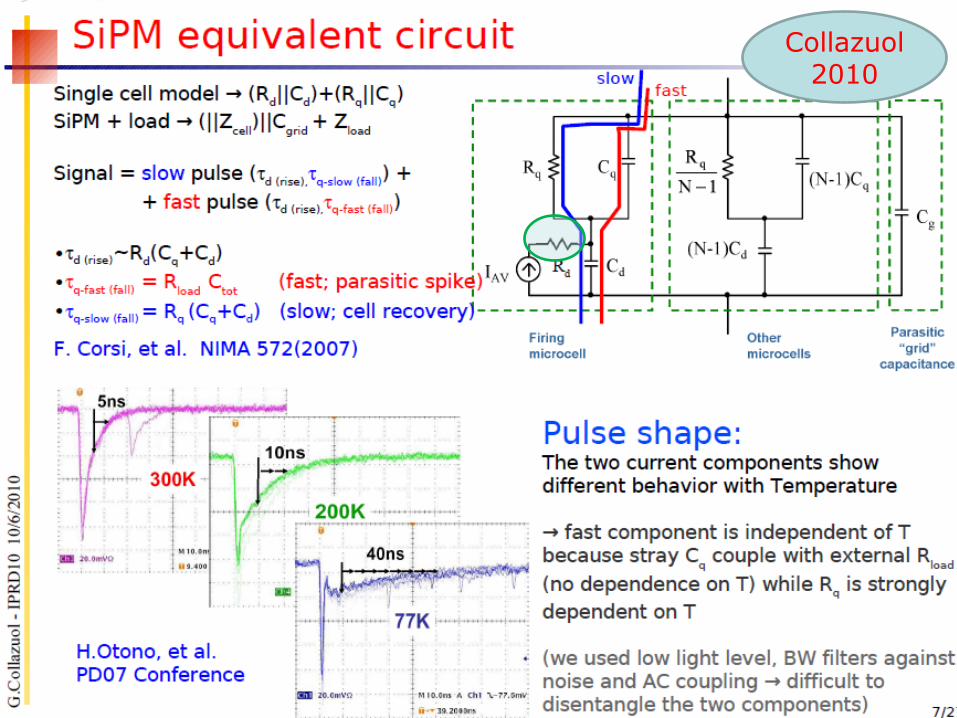
15 jun 2012 CdLT Photodet conference
Collazuol 2010
15 jun 2012 CdLT Photodet conference
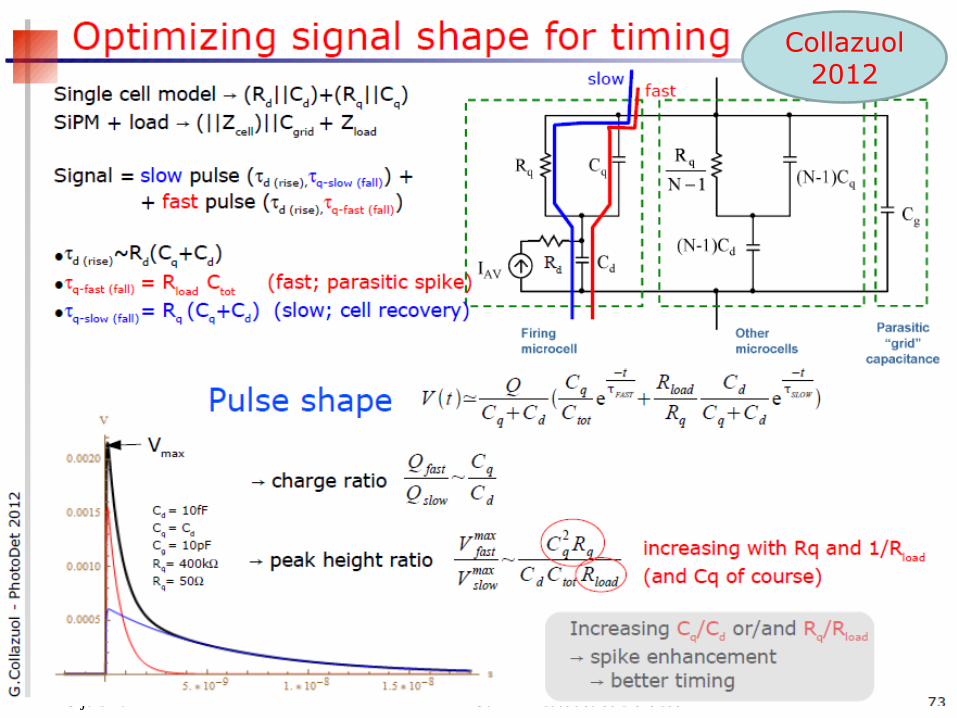
Collazuol 2012

SiPM impedance and model
• RLC too simple, inaccurate at high frequency
• CdRqCqLR OK
– May better explain HF noise behaviour
15 jun 2012 CdLT Photodet conference
1
10
100
1000
1.00 10.00 100.00 1,000.00
Measured impedance
MPPC HPK 3x3 mm
Line : C = 320 pF
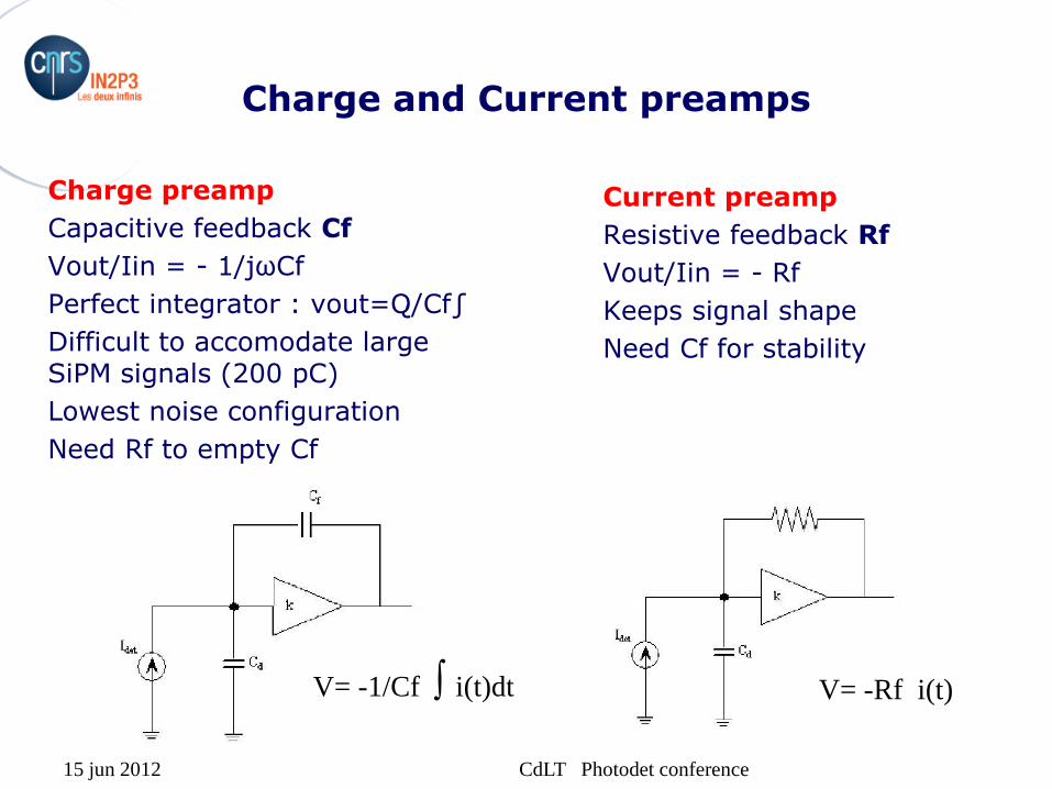
Charge and Current preamps
Charge preamp
Capacitive feedback Cf
Vout/Iin = - 1/jωCf
Perfect integrator : vout=Q/Cf∫
Difficult to accomodate large SiPM signals (200 pC)
Lowest noise configuration
Need Rf to empty Cf
Current preamp
Resistive feedback Rf
Vout/Iin = - Rf
Keeps signal shape
Need Cf for stability
V= -1/Cf ∫ i(t)dt V= -Rf i(t)
15 jun 2012 CdLT Photodet conference
15 jun 2012 CdLT Photodet conference
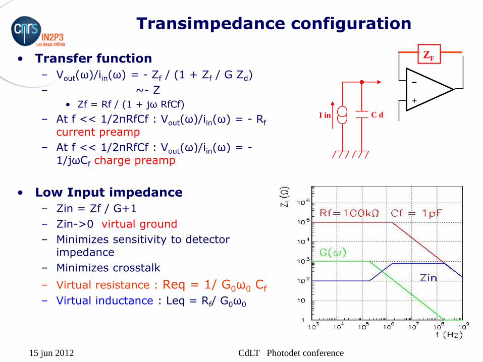
Transimpedance configuration
• Transfer function
– Vout(ω)/iin(ω) = - Zf / (1 + Zf / G Zd)
– ~- Z
• Zf = Rf / (1 + jω RfCf)
– At f << 1/2πRfCf : Vout(ω)/iin(ω) = - Rf current preamp
– At f << 1/2πRfCf : Vout(ω)/iin(ω) = - 1/jωCf charge preamp
• Low Input impedance
– Zin = Zf / G+1
– Zin->0 virtual ground
– Minimizes sensitivity to detector impedance
– Minimizes crosstalk
– Virtual resistance : Req = 1/ G0ω0 Cf
– Virtual inductance : Leq = Rf/ G0ω0
- +
ZF
I in C d

15 jun 2012 CdLT Photodet conference
Stabilisying the transimpedance amplifier
• RLC circuit with capacitive detector
– Resonant frequency : fres = 1/2π √LeqCd
– Quality factor : Q = 1/Cf √(Cd/Rf G0ω0)
– Q > 1/2 -> ringing
– Damping : Q=1/2
=> Cf=2 √(Cd/Rf G0ω0)
– Example :
• LM741 (G0ω0=107) : Cf=10pF
• OP620 (G0ω0=109) : Cf=0.3pF
• In frequency domain
– H(jω) = -Rf / (1 + jω RfCd/G(ω))
= -Rf / (1 + jω RfCd/G0 - ω2 RfCd /G0ω0)

15 jun 2012 CdLT Photodet conference
Transimpedance amplifier
• Transimpedance :
– Vout(ω)/iin(ω) = - Zf / (1 + Zf / G Zd)
– Zf = Rf / (1 + jω RfCf)
– G(ω) = G0/(1 + j ω/ω0)
– H ~ - Rf / (1 + jω RfCd/G0 - ω2 RfCd /G0ω0)
• 2nd order system, easily oscillatory
– Damped with Cf, but BW limitation at RfCf
• Input impedance : Zin = Zf/G : Inductive term because G(ω)
– Rin = RfG0, Lin= Rf/G0ω0
– with Rf=500 Ω, G0=100, G0ω0=10GHz, get Rin=5 Ω and Lin=3 nH
• Similar frequency response as current conveyor
– More unstable
– Potentially lower power
- +
ZF
I in C d

15 jun 2012 CdLT Photodet conference
Charge vs Current preamps
• Charge preamps
– Best noise performance
– Best with short signals
– Best with small capacitance
• Current preamps
– Best for long signals
– Best for high counting rate
– Significant parallel noise
• Charge preamps are not slow, they are long
• Current preamps are not faster, they are shorter (but easily unstable)
Current Charge

High speed configurations
• Open loop configurations : current conveyors, RF amplifiers
• Usually designed at transistor level MOS or SiGe (ex PETIROC)
15 jun 2012 CdLT Photodet conference
• Current conveyors
• Small Zin : current sensitive input
• Large Zout : current driven output
• Unity gain current conveyor
• E.g. : (super) common-base configuration
• Low input impedance : Rin=1/gm
• Transimpedance : Rc
• Bandwitdth : 1/2πRcCμ > 1 GHz
• RF amplifiers
• Large Zin : voltage sensitive input
• Large Zout : current driven output
• Current conversion with resistor RS
• E.g. common-emitter configuration
• Transimpedance : -gmRcRs
• Bandwitdth : 1/2πRsCt
RS=50 Ω I in C d I in C d

Noise and jitter
• Electronics noise dominated by series noise en
– Large detector capacitance
– For voltage preamp and load resistor RL,
– Output rms noise Vn²=(en²+4kTRs) G² π/2*BW-3dB
– Typical values : Rs=50 Ω, en=1 nV/√Hz Vn=1 mV for G=10, BW=1GHz
– For current sensitive preamps, possible noise peaking due to Cd
• Jitter
– Part due to electronics noise :
– σt = σv / (dV/dt)
– Minimized by increasing BW
15 jun 2012 CdLT Photodet conference

A few (personal) comments
• Strong push for high speed front-end > GHz
– Essential for timing measurements
– Several configurations to get GBW > 10 GHz
– Optimum use of SiGe bipolar transiistors
• Voltage sensitive front-end
– Easiest : 50Ω termination, many commercial amplifiers (mini circuit…)
– Beware of power dissipation
– Easy multi-gain (time and charge)
• Current sensitive front-end
– Potentially lower noise, lower input impdance
– Largest GBW product
• In all cases, importance of reducing stray inductance
15 jun 2012 CdLT Photodet conference

Stefan Ritt 18/33 15 jun 2012 CdLT Photodet conference
Waveform digitizers [S. Ritt]
4 channels 5 GSPS 1 GHz BW 8 bit (6-7) 15k€
4 channels 5 GSPS 1 GHz BW 11.5 bits 900€ USB Power
FADCs
• 8 bits – 3 GS/s – 1.9 W 24 Gbits/s
• 10 bits – 3 GS/s – 3.6 W 30 Gbits/s
• 12 bits – 3.6 GS/s – 3.9 W 43.2 Gbits/s
• 14 bits – 0.4 GS/s – 2.5 W 5.6 Gbits/s
1.8 GHz! 24x1.8 Gbits/s
PX1500-4: 2 Channel 3 GS/s 8 bits
1/10 k€/ch

Stefan Ritt 19/33 15 jun 2012 CdLT Photodet conference
Switched Capacitor Array (Analog Memory)
Shift Register Clock
IN
Out
“Time stretcher” GHz MHz
Waveform stored
Inverter “Domino” ring chain
0.2-2 ns
FADC 33 MHz
10-100 mW
dts dtd

Stefan Ritt 20/33 15 jun 2012 CdLT Photodet conference
How is timing resolution affected?
voltage noise Du
timing uncertainty Dt
signal height U
dBs ffU
ut
33
1
DD
U Du fs f3db Dt
100 mV 1 mV 2 GSPS 300 MHz ∼10 ps
1 V 1 mV 2 GSPS 300 MHz 1 ps
1V 1 mV 10 GSPS 3 GHz 0.1 ps
today:
optimized SNR:
next generation:
Assumes zero aperture jitter

Stefan Ritt 21/33 15 jun 2012 CdLT Photodet conference
• CMOS process (typically 0.35 … 0.13 mm) sampling speed
• Number of channels, sampling depth, differential input
• PLL for frequency stabilization
• Input buffer or passive input
• Analog output or (Wilkinson) ADC
• Internal trigger
• Exact design of sampling cell
Design Options
PLL
ADC
Trigger

Stefan Ritt 22/33 15 jun 2012 CdLT Photodet conference
Switched Capacitor Arrays for Particle Physics
STRAW3 TARGET LABRADOR3 AFTER NECTAR0 SAM
E. Delagnes D. Breton CEA Saclay
DRS1 DRS2 DRS3 DRS4
G. Varner, Univ. of Hawaii
• 0.25 mm TSMC • Many chips for different projects
(Belle, Anita, IceCube …)
• 0.35 mm AMS • T2K TPC, Antares, Hess2,
CTA
H. Frisch et al., Univ. Chicago
PSEC1 - PSEC4
• 0.13 mm IBM • Large Area Picosecond
Photo-Detectors Project (LAPPD)
2002 2004 2007 2008
• 0.25 mm UMC • Universal chip for many applications • MEG experiment, MAGIC, Veritas,
TOF-PET
Stefan Ritt R. Dinapoli PSI, Switzerland
drs.web.psi.ch
www.phys.hawaii.edu/~idlab/ matacq.free.fr psec.uchicago.edu
Poster 232
Poster 15, 106

Stefan Ritt 23/33 15 jun 2012 CdLT Photodet conference
Digital Pulse Processing (DPP)
C. Tintori (CAEN) V. Jordanov et al., NIM A353, 261 (1994)

Stefan Ritt 24/33 15 jun 2012 CdLT Photodet conference
Things you can buy
• DRS4 chip (PSI) • 32+2 channels • 12 bit 5 GSPS • > 500 MHz analog BW • 1024 sample points/chn.
• 110 ms dead time
• MATACQ chip (CEA/IN2P3) • 4 channels • 14 bit 2 GSPS • 300 MHz analog BW • 2520 sample points/chn. • 650 ms dead time
• DRS4 Evaluation Board • 4 channels • 12 bit 5 GSPS • 750 MHz analog BW • 1024 sample points/chn. • 500 events/sec over USB 2.0
• SAM Chip (CEA/IN2PD) • 2 channels • 12 bit 3.2 GSPS • 300 MHz analog BW • 256 sample points/chn. • On-board spectroscopy

Stefan Ritt 25/33 15 jun 2012 CdLT Photodet conference
Plans
counte
r
latc
hla
tch
latc
hwrite
pointer
readpointer
digital readout
analog readout
trigger
FPGA
• Self-trigger writing of 128 short 32-bin segments (4096 bins total)
• Storage of 128 events • Accommodate long trigger latencies • Quasi dead time-free up to a few MHz, • Possibility to skip segments
→ second level trigger
• Attractive replacement for CFG+TDC
• First version planned for 2013
• Dual gain channels • Dynamic power management (Read/Write
parts) • Region-of-interest readout
DRS5 (PSI)
CEA/Saclay

Comments
• Trends
– Reduce dead time
– increase analog bandwidth
– Increase depth, give more latency
– Include high speed low noise preamps (NECTAR…)
• Comments
– Unbeatable for pulse shape analysis or discrimination
– Ultra low timing measurements (ps)
– More power hungry than dedicated front-end (many CdV/dt…), needs careful study for large systems (>> kch)
15 jun 2012 CdLT Photodet conference

15 jun 2012 CdLT Photodet conference
SiPM readout chips
Chip name group year Technology channels Application
FLC_SiPM OMEGA 2004 BiCMOS
0.8µm
18 ILC HCAL
NINO CERN 2004 CMOS 0.25µm 8 ALICE TOF
MAROC2 OMEGA 2006 SiGe 0.35µm 64 ATLAS lumi
SPIROC OMEGA 2007 SiGe 0.35µm 36 ILC HCAL
PETA Heidelberg 2008 CMOS 0.18µm 40 PET
RAPSODI Krakow 2008 CMOS 0.35µm 2 Snooper
BASIC Bari 2009 CMOS 0.35µm 32 PET
SPIDER Ideas 2009 CMOS 0.35µm 64 Spider rich
© W. Kucevisz (Krakow)

Precursor : CALICE AHCAL (2004)
• Hadronic calorimeter prototype for the ILC : 1 cubic metre, 38 layers, 2cm steel plates
• 8000 tiles with SiPMs fabricated by MePHY group
15 jun 2012 CdLT Photodet conference
Mechanics and front end boards: DESY SiPM : Mephy Pulsar Moscow Front end ASICs: LAL
FLC_SiPM
ASIC Mephy SiPM

FLC_SiPM
• Voltage variable gain amplifier + variable CRRC² shaper
• Input 5V 8bit-DAC for bias point adjustment
• 18 channels, Analogue readout, 12 mW/ch
• 1000 chips produced in AMS BiCMOS 0.8 µm
15 jun 2012 CdLT Photodet conference

15 jun 2012 CdLT Photodet conference
Successors : OMEGA/Orsay « ROC chips »
• Move to Silicon Germanium 0.35 µm BiCMOS technology in 2004
• Readout for MaPMT and SiPM for ILC calorimeters and other applications
• Very high level of integration : System on Chip (SoC)
HARDROC2
SPIROC2
MAROC3
SPACIROC
SKIROC2
MICROROC1
PARISROC2
http://omega.in2p3.fr
Chip detector ch DR (C)
MAROC PMT 64 2f-50p
SPIROC SiPM 36 10f-200p
SKIROC Si 64 0.3f-10p
HARDROC RPC 64 2f-10p
PARISROC PM 16 5f-50p
SPACIROC PMT 64 5f-15p
MICROROC µMegas 64 0.2f-0.5p

CdLT Photodet conference
SPIROC for SiPM
• SPIROC : Silicon Photomultiplier Integrated Readout
Chip to read out the analog hadronic calorimeter for
CALICE (ILC)
• Ultra low-power 36-Channel ASIC
• Internal input 8-bit DAC (0-5V) for individual SiPM gain adjustment
• Energy measurement : 14 bits, 1 pe to 2000 pe
– pe/noise ratio : ~11
• Auto-trigger on MIP or on single photo-electron
– Auto-Trigger on 1/3 pe (50fC)
• Time measurement :
– 12-bit Bunch Crossing ID (coarse time)
– 12-bit step~1 ns TDC->TAC (fine time)
– Analog memory for time and charge measurement : depth = 16
– Low consumption : ~25 µW per channel (in power pulsing mode)
– 4kbytes internal memory and daisy chain readout
M. Bouchel, S. Callier, F. Dulucq, J. Fleury, J.-J. Jaeger, C. de La Taille, G.
Martin-Chassard, and L. Raux, “SPIROC (SiPM integrated read-ou chip):
Dedicated very front-end electronics for an ILC prototype hadronic
calorimeter with SiPM read-out,” J. Instrum. 6(01), C01098 (2011).
(0.36m)2 Tiles + SiPM + SPIROC (144ch)

CdLT Photodet conference
SPIROC: trigger efficiency measurements
Pedestal
50fC
injected
36-channel S-curves: trigger efficiency
versus threshold (1 LSB = 2 mV)
MIP response in DESY
6 GeV electron testbeam
SiPM SPECTRUM with Autotrigger
linearity using the auto gain mode
and internal ADC
©M. Reinecke (DESY)
33
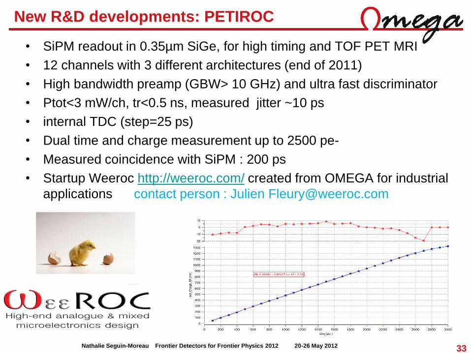
New R&D developments: PETIROC
Nathalie Seguin-Moreau Frontier Detectors for Frontier Physics 2012 20-26 May 2012
• SiPM readout in 0.35µm SiGe, for high timing and TOF PET MRI
• 12 channels with 3 different architectures (end of 2011)
• High bandwidth preamp (GBW> 10 GHz) and ultra fast discriminator
• Ptot<3 mW/ch, tr<0.5 ns, measured jitter ~10 ps
• internal TDC (step=25 ps)
• Dual time and charge measurement up to 2500 pe-
• Measured coincidence with SiPM : 200 ps
• Startup Weeroc http://weeroc.com/ created from OMEGA for industrial
applications contact person : Julien [email protected]

15 jun 2012 CdLT Photodet conference
T2K SiPM FGD

35
AFTER: Asic For TPC Electronic Read-out
Technology: AMS CMOS 0.35mm
Area: 7546mm x 7139 mm
LQFP 160 pins; Plastic
dimensions: 30mm x 30mm
thickness: 1.4mm
pitch: 0.65mm
Number of transistors: 400,000
Power consumption: 5-7 mW/ch
6000 chips manufactured and tested
Purpose: - Collect, preamplify and shape of the detector signal.
-Continuously sample the shaped signal in an 511-cell analog circular buffer (1MHz to 100MHz rate)
-After the sampling has been stopped by an external request, read back the analog memory (partially or
totally) at a rate up to 20 MHz.
Allows to de-correlate the sampling and digitization rates.
An oscilloscope on each channel.
72chx511 cells
0 511
Stop
(trigger)
Read Phase
ci ci+1
Write Phase
The readout time is proportionnal to the number
of sample read : 2ms is for 511 cells
AFTER: ROOffset=0
AGET: ROOffset is programmable

36
AFTER Main Features: 72 low noise FE channels associated with a 511-cell SCA
Main features:
• Input Current Polarity: positive or negative
• 72 Analog Channels
• 4 Gains: 120fC, 240fC, 360fC & 600fC
• 16 Peaking Time values: (100ns to 2µs)
• 511 analog memory cells / Channel:
Fwrite: 1MHz-100MHz; Fread: 20MHz
AFTER
511 cells
SCA FILTER
100ns<tpeak<2us
CSA
1 channel
x72(76)
BUFFER
SCA MANAGER SLOW CONTROL
Serial Interface
W / R
Mode
CK
CK
ADC
TEST
In Test
120fC<Cf<600fC
Power Supply Reference Voltage Reference Current
Asic Spy Mode
CSA;CR;SCAin (N°1)
Power On
Reset
• Optimized for 20-30pF detector capa
• 12-bit dynamic range
• Slow Control
• Power on reset
• Test modes
• Spy mode on channel 1:
CSA, CR or filter out
No onchip zero suppress.
No auto triggering.
No selective readout.
IEEE Trans. Nucl Sci, June 2008
15 jun 2012

37
Pulse Shape + linearity
Perfectly working for a 100MHz wck Digitized signal with various peaking time
Integral Non Linearity <1.2% 300 e’ < ENC < 2000 e

38
The children of AFTER
GET (ANR): Generic electronics for nuclear physics
(with GANIL, CENBG, NSCL)
AGET chip:
Auto-trigger, Multiplicty output, 1th/channel
On-chip zero supress,
Target: ~30 000 –channel active target TPC
CLAS12 (Jefferson Lab): Trajectographe Micromégas (2014)
30 000 voies.
ASIC DREAM:
Deadtime « free » architecture,
L0 latency + event buffer
Auto-triggering capabilities
AFTER (T2K)
120K channels
Similar FE + SCA architecture
New common features: • Possibility to bypass CSA and/or shaper to connect directly an external
front-end or (photo)-detector &
• programmable gain & for each channel
39
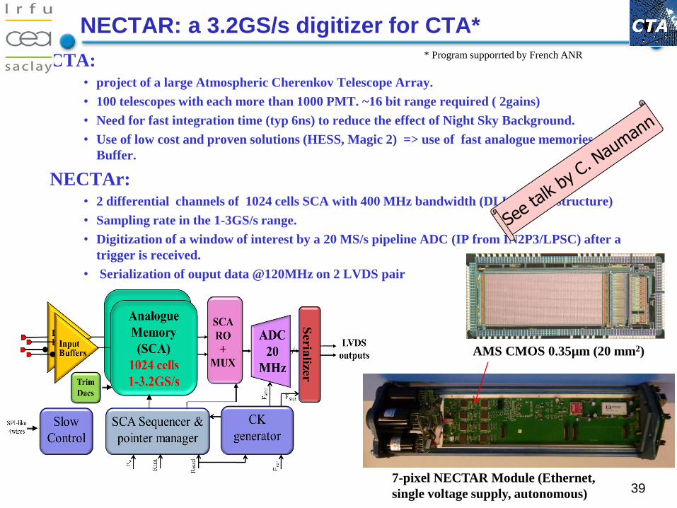
NECTAR: a 3.2GS/s digitizer for CTA*
CTA: • project of a large Atmospheric Cherenkov Telescope Array.
• 100 telescopes with each more than 1000 PMT. ~16 bit range required ( 2gains)
• Need for fast integration time (typ 6ns) to reduce the effect of Night Sky Background.
• Use of low cost and proven solutions (HESS, Magic 2) => use of fast analogue memories as L1
Buffer.
NECTAr: • 2 differential channels of 1024 cells SCA with 400 MHz bandwidth (DLL-matrix structure)
• Sampling rate in the 1-3GS/s range.
• Digitization of a window of interest by a 20 MS/s pipeline ADC (IP from IN2P3/LPSC) after a
trigger is received.
• Serialization of ouput data @120MHz on 2 LVDS pair
AMS CMOS 0.35µm (20 mm2)
* Program supporrted by French ANR
7-pixel NECTAR Module (Ethernet,
single voltage supply, autonomous)

40
NECTAR performance (measured on the NECTAR module)

NINO
Chip designed by CERN group for ALICE TOF RPCs [ F. Anghinolfi, P. Jarron et al. NINO: an ultra-fast and low-power front-end amplifier/discriminator ASIC designed for the
multigap resistive plate chamber, NIM A, 2004, Vol. 533 page 183-187 ]
8 channels amplifier and discriminator Common grid current conveyor, high speed differential discriminator
High speed time measurement (10 ps), Amplitude through time over threshold technique
Pd = 25 mW/ch, Manufactured in IBM 0.25 um
15 jun 2012 CdLT Photodet conference

NINO for PET
Application for TOF-PET [P . Jarron, E. Auffray, S.E. Brunner, M. Despeisse, E. Garutti, M. Goettlich, H. Hillemanns, P. Lecoq, T. Meyer, F. Powolny, W. Shen, H.C.
Schultz-Coulon, C. Williams - Time based readout of a silicon photomultiplier (SiPM) for Time Of Flight Positron EmissionTomography
(TOF-PET) - 2009 IEEE Nuclear Science Symposium Conference Record, p. 1212 and NIM 617 (2010), p. 232
Differential connection of NINO to SiPM
NINO followed by CERN 25 ps HPTDC
15 jun 2012 CdLT Photodet conference

Performance
Jitter measured : 390 ps
Now in : 32 channels [M. Despeisse, F. Powolny, J. Lapington, P. Jarron : Multi-Channel Amplifier-Discriminator for Highly Time-Resolved Detection. IEEE
Trans. Nucl. Sci. 58 (2011) 202-208 ] 15 jun 2012 CdLT Photodet conference
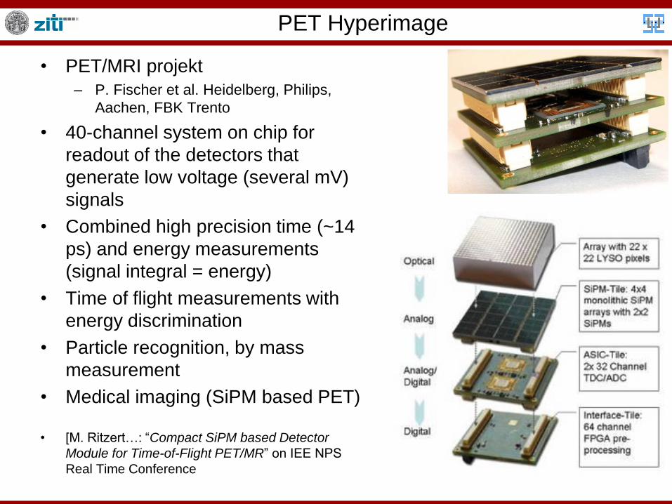
PET Hyperimage
• PET/MRI projekt
– P. Fischer et al. Heidelberg, Philips,
Aachen, FBK Trento
• 40-channel system on chip for
readout of the detectors that
generate low voltage (several mV)
signals
• Combined high precision time (~14
ps) and energy measurements
(signal integral = energy)
• Time of flight measurements with
energy discrimination
• Particle recognition, by mass
measurement
• Medical imaging (SiPM based PET)
• [M. Ritzert…: “Compact SiPM based Detector
Module for Time-of-Flight PET/MR” on IEE NPS
Real Time Conference

Photographs of the chip
hit logic
time latches fine
time latches coarse
integrator
1 of 40 channels
DAC
Threshold
Comp
Simple Readout: latches + Shift Reg.
Logic
Hit SerOut Reset, Clock
2
Integration Time Window
DAC
Discriminator
01001010
01011000
• PETA chip : Positioning, Energy and Timestamping Asic • P. Fischer, I. Peric, M. Ritzert, and M. Koniczek -Fast Self Triggered Multi Channel Readout ASIC for Time- and
Energy Measurement – IEEE TRANSACTIONS ON NUCLEAR SCIENCE, VOL. 56, NO. 3, p.1153
• 40 differential channels that perform time and energy measurements
• fast time stamp generators, that can be synchronized by in-chip PLL
• PLL clock frequency is ~770MHz leading to 40ps bin width

46
Integrator – main blocks
1
Comparator
4
Integrator
A1 A3
Reset
4
3
12
DAC
C1
R3
Stop
Output
2
Offset Corr.
TC
Start
6
R2
C2
5
Delay elements
Amplifier
3
A2
Start
9
10 8 7
C3
C4
R4 2
R1
Input
1
11
1) Input resistor R1 converts the input voltage into current
2) A1 - integrator
3) Offset correction circuit
4) A2 - difference amplifier measures the change of voltage 4 (integral)
and converts it to current IR4
5) A3 - current-mode comparator compares IR4 with the DAC current

47
Integrator performance
ADC code - mean value vs pulse length
0
500
1000
1500
2000
2500
3000
0 100 200 300 400 500
ADC code sigma value vs pulse length
6,6
6,7
6,8
6,9
7
7,1
7,2
7,3
0 100 200 300 400 500
Integral of the input (single ended) pulse with 100mv
Amplitude and variable width
ns ns
Noise in LSB – full range - 4096
ADC linearity
7.2
7.0
48
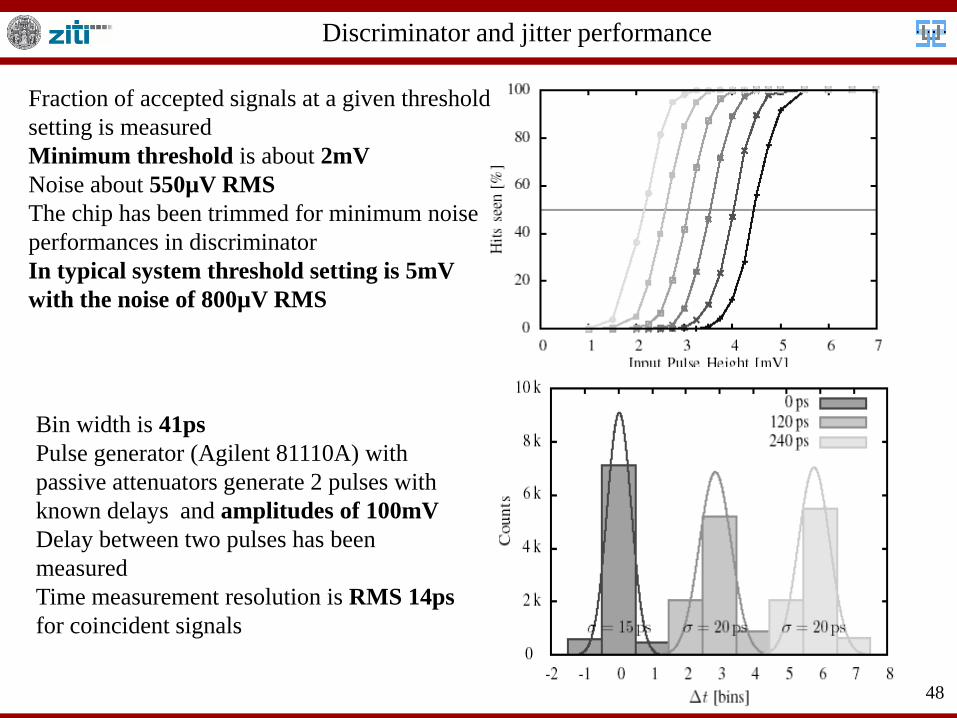
Discriminator and jitter performance
Fraction of accepted signals at a given threshold
setting is measured
Minimum threshold is about 2mV
Noise about 550µV RMS
The chip has been trimmed for minimum noise
performances in discriminator
In typical system threshold setting is 5mV
with the noise of 800µV RMS
Bin width is 41ps
Pulse generator (Agilent 81110A) with
passive attenuators generate 2 pulses with
known delays and amplitudes of 100mV
Delay between two pulses has been
measured
Time measurement resolution is RMS 14ps
for coincident signals

Politecnico di Bari (F. Corsi, M. Foresta, C. Marzocca, G. Matarrese)
Universita di Pisa (N. Belcari, M. G. Bisogni, A. Del Guerra, S. Marcatili)
F. Corsi et al., A “Front-‐end Electronics for Silicon Photo-‐Multipliers Coupled to Fast
Scintillator”, 2010 IEEE Nuclear Science Symposium (NSS-‐MIC’2010) Conference Record,
Knoxville, TN (USA), October 30-‐ November 6, 2010.
32 channel readout ASIC for PETMRI
Simultaneous charge and time measurement with current conveyor
BASIC32
8th International Meeting on Front-End Electronics, May 24-27, 2011, Bergamo
15 jun 2012 CdLT Photodet conference

Structure of the analog channel
8-bit
DAC
4-bit
curren
tDAC
SiPM
VREF
VBIAS
M1
M2
MO1 MO2
feedbac
k
current discriminator
CSA
VDDA
IBIAS 1:N
output
curren
t
1:M
output
curren
t
baseline holder
peak detector
CF
RF
MBL VBL=300mV
CBL
+
_
+
_
trigger
output
charge
output
Technology:
0.35um standard CMOS
8th International Meeting on Front-End Electronics, May 24-27, 2011, Bergamo
15 jun 2012 CdLT Photodet conference

Main features and parameters of the analog channel
Current buffer
Small signal bandwidth: 250MHz
(with a 30pF detector)
Low input resistance: 17W
Scaling factors: N=10, M= 20
VREF variable in the range 1V÷2V
Total current consumption: 800uA
Fast Current Discriminator
Leading edge
Trise ≈ 300ps
Threshold programmable :
4-bit current DAC from 0 to 40mA
CSA
Continuous passive reset
Variable gain: CF=1pF, 2pF, 3pF
Damping time constant: 200ns
Output voltage range: 0.3V ÷ 2.7V
Baseline holder
Very slow feedback loop
“Ad hoc” techniques to reproduce
large time constants
Small baseline shifts at high event
rates (-1mV @ 100kHz, full
dynamic)
8th International Meeting on Front-End Electronics, May 24-27, 2011, Bergamo
15 jun 2012 CdLT Photodet conference

Experimental results: injection capacitance, gain , timing
8th International Meeting on Front-End Electronics, May 24-27, 2011, Bergamo
15 jun 2012 CdLT Photodet conference
Timing accuracy : σ = 132 ps
Spectrum with
22Na source
Energy resolution 11%
Time resolution :
1.2 ns FWHM
Timing accuracy of the fast-OR signal
vs the trigger provided by the PMT Low threshold level:
timing accuracy 1.2 ns FWHM
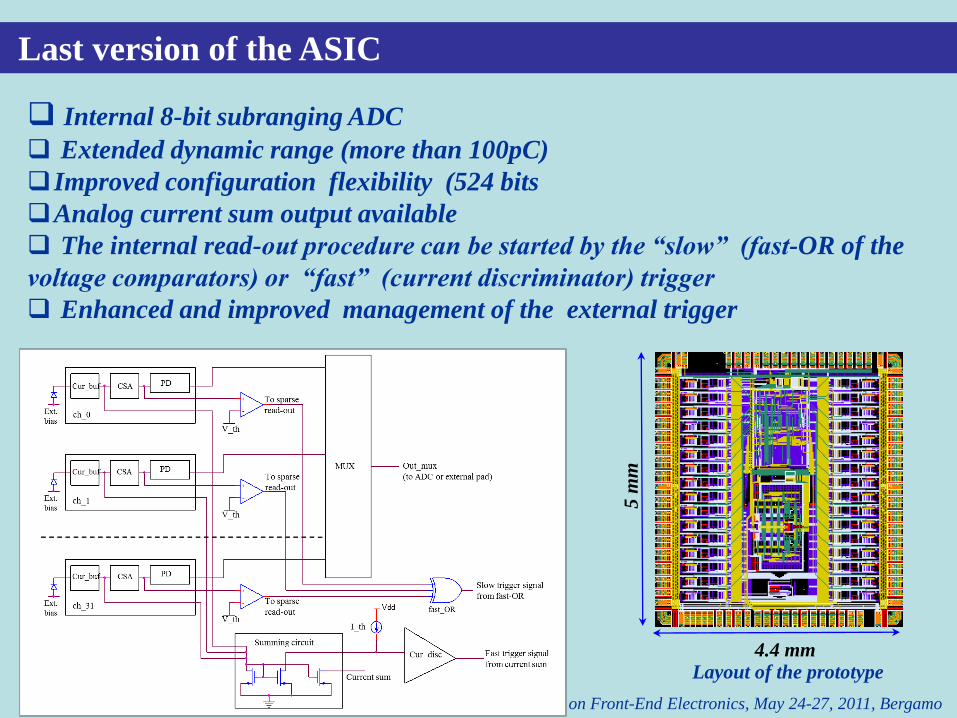
Last version of the ASIC
8th International Meeting on Front-End Electronics, May 24-27, 2011, Bergamo
4.4 mm 5
mm
Layout of the prototype
Internal 8-bit subranging ADC
Extended dynamic range (more than 100pC)
Improved configuration flexibility (524 bits
Analog current sum output available
The internal read-out procedure can be started by the “slow” (fast-OR of the
voltage comparators) or “fast” (current discriminator) trigger
Enhanced and improved management of the external trigger

15 jun 2012 CdLT Photodet conference
RAPSODI
ASIC is a 2 channel SiPM readout chip for energy measurement, made in 0,35 µm CMOS AMS technology (2009)
Each channel measures the amplitude of the signal from SiPM and converts it in 7-bit ADC. The channels can work separately or in coincidence mode.
FPGA Treshold
correction
PZC, Gain correction
Coincidence Block
Comp
Comp
Peak Detector and Hold
ADC 7 bits Ampl
Peak Detector and Hold ADC 7 bits Ampl
Integrated Circuit
Coinc. timing set.
R. Mos, J. Barszcz, M.Jastrzab, W.Kucewicz, J. Mlynarczyk, E.Raus, M. Sapor - Front-End electronics for Silicon Photomultiplier detectors implemented in CMOS VLSI integrated circuit - Electrical Review NR 11a (2010), p.79
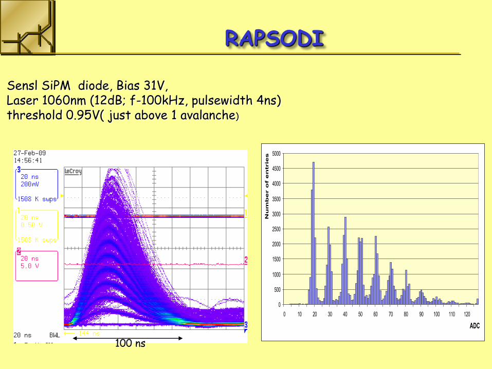
RAPSODI
100 ns
Sensl SiPM diode, Bias 31V, Laser 1060nm (12dB; f-100kHz, pulsewidth 4ns) threshold 0.95V( just above 1 avalanche)
0
500
1000
1500
2000
2500
3000
3500
4000
4500
5000
0 10 20 30 40 50 60 70 80 90 100 110 120
ADC
Nu
mb
er o
f e
ntrie
s

SPIDER VA-TA HDR 16
• D. Meier et al. GM-IDEAS Norway, INFN Siena, INFN Pisa
• Chip VATA64-HDR16 was developed for SiPM applied in Ring Imaging Cherenkov Detector of SPIDER (Space Particle IDentifiER) Experiment
• [ M.G. Baglieis et al. «A custom front-end ASIC for the readout and timing of 64 SiPM» NIM Nuclear
Physics B (Proc. Suppl.) 215 (2011) 344–348 ]
15 jun 2012 CdLT Photodet conference

VA-TA performance
• Dynamic range : 12 pc
• Noise : 1 fC
15 jun 2012 CdLT Photodet conference
TAC linearity
Time jitter : σ = 160 ps

15 jun 2012 CdLT Photodet conference
SiPM readout chips
Chip
name
# of channe
ls ADC
Power /channel
Dynamic range
Input resistance
noise jitter
FLC_SiPM 18 n 10 mW 100 pC 50 W
ext 15 fC
MAROC2 64 y 20 mW 80 pC 50 W 1 fC 120 ps
SPIROC 36 y 5 mW 200 pC 50 W
ext 5-10 fC 100 ps
NINO 8 n 30 mW 300 pC 20 W 5 fC 20 ps
PETA 40 y 30 mW 8 bit 50 W
ext x fC 40 ps
BASIC 32 y 70 pC 17 W 50 fC 120 ps
VATA64-HDR16 64 n 16 mW 15 pC 1 fC 160 ps
RAPSODI 2 y 100 mW 100 pC 20 W
© W. Kucevisz (Krakow)

Digital SiPM
15 jun 2012 CdLT Photodet conference

15 jun 2012 CdLT Photodet conference

15 jun 2012 CdLT Photodet conference
Fm M. Heller PHOTODET 2012

Analog and digital SiPMs
• Superior timing resolution shown by dSiPM
– Gets rid of stray inductance
– Uses the first photons
• Is the aSiPM already dead ?
– Cost effective solution for large number of channels, with 100 ps
– Needs dedicated (optimized) readout ASIC
– Power dissipation and system level issues are easier
15 jun 2012 CdLT Photodet conference

Conclusion
• Spectacular progress of SiPM/MPPC sensors
– Larger area, matrixes, lower noise, better PDE…
– Already equiping large experiments
• Importance of readout electronics
– Timing measurements
– Large dynamic range measurements
– high integration => cost reduction
• Trends for readout electronics
– High speed electronics (> GHz)
– High level of integration (SoC)
– Integration sensor/readout (digital SiPM)
– Importance of low power design
15 jun 2012 CdLT Photodet conference

backup
15 jun 2012 CdLT Photodet conference

15 jun 2012 CdLT Photodet conference
RAPSODI
1. R. Mos, J. Barszcz, M.Jastrzab, W.Kucewicz, J. Mlynarczyk, E.Raus, M. Sapor - Front-End electronics for Silicon Photomultiplier detectors implemented in CMOS VLSI integrated circuit - Electrical Review NR 11a (2010), p.79
2. R. Mos, J. Barszcz, M.Jastrzab, W.Kucewicz, J. Mlynarczyk, E.Raus, M. Sapor - Front-end Electronics for Silicon Photomultipliers Implemented in CMOS VLSI – Preceedings of MIXDES 2009, 16th International Conference "Mixed Design of Integrated Circuits and Systems", June 25-27, 2009, p. 266
3. W. Kucewicz, J. Barszcz, J. Juraszek, R. Mos, M. Sapor - The two channel CMOS converter for silicon photomultiplier – Proceedings of ICSES 2008 - International conference on Signals and Electronic Systems : September 14–17, 2008, p. 165
ASIC developed within the 6 FP RAPSODI for MICROSNOOPER (portable real time meter to detect and identify any type of radiation)

15 jun 2012 CdLT Photodet conference
RAPSODI
Two stage amplifier allows to switch ranges between 1, 10 and 100 pC. The PZC block moderate the fallowing edge of the signal.

a-SiPM versus d-SiPM
15 jun 2012 CdLT Photodet conference
TDC TDC TDC TDC
d-SiPM
“endoTOFPET”
∑
a-SiPM The a-SiPM: • low rise time;
• high capacitance;
• reasonable fill factor (FF);
• mature technology;
• commercially available
• time over threshold discr.
• standard (HP)TDC readout.
• very low rise time; • individual SPAD readout
single photon counting optimum timing
• high functionality • ambitious/risky • novel technology • optimized for endoscope
The d-SiPM:

a-SiPM: Test Scenario
15 jun 2012 CdLT Photodet conference
• For an intrinsic SiPM timing evaluation, see poster by Stefan Gundacker/CERN;
• Coincidence time resolution (CTR) measured with scintillating “reference” crystals and the NINO amplifier/discriminator;
• Use high-BW scope (LeCroy DDA 735Zi, 40GS/s) or HPTDC.
22Na-Source
(2 x 2 x 10 mm3)
CTR measured with two same SiPMs: • Crystals are wrapped and mounted
“small-face-to-SiPM” with grease;
• Spectra are refined through photo-peak selection.
Sample CTR Spectrum NINO chip: • Fast discrimin. (3GHz BW)
• Signal peaking time: <1ns
• Output time jitter: ≤ 25ps
• Differential architecture

a-SiPM: Evaluation & Selection
• Suitable SiPMs are commercial MPPCs by Hamamatsu Photonics;
• Evaluation of photodetectors via measurement of the (CTR):
MPPC
S10931- # SPADs
Fill Factor
[%]
VManuf.
[V]
Voptimum
[V]
DCR*)
[MHz]
NINO
Thr. [mV]
CTR FWHM
[ps]
-025P 14’400 30.8 71.49
71.44 73.0 3.2 150 340±9
-050P 3’600 61.5 72.11
72.09 72.4 1.1
1.0 100 220±4
-100P 900 78.5 70.81
70.87 70.3 9.0
9.5 300 280±9
15 jun 2012 CdLT Photodet conference
*) DCR = Dark Count Rate
3mm
3mm
Note: Optimization of
SiPMs done with non-
optimized crystals.
DC
R [
MH
z]
CT
R F
WH
M [
ps]
CT
R F
WH
M [
ps]
MPPC S10931-050P
S. Gundacker et al., “A Systematic Study to Optimize SiPM Photo-Detectors for Highest Time Resolution in PET” (TNS-00225-2011)
Bias Scan Threshold Scan

d-SiPM for endo-TOFPET-US
15 jun 2012 CdLT Photodet conference
• Capability to gather the statistics of the first individual photons that reach a cluster*);
• Intrinsically best timing performance attractive for TOF;
• Balance functionality and PDE;
• Design must adapt to process-specific effects: • high DCR from tunneling and trap-assisted noise;
• after-pulsing;
• lower PDP than with conventional a-SiPMs.
• Requires multi-parameter optimization/simulation.
*) M. Fishburn & E. Charbon, “System Tradeoffs in Gamma-Ray Detection Utilizing SPAD Arrays and Scintillators”, IEEE-TNS, VOL. 57, NO. 5, OCTOBER 2010.
S. Seifert et al., “The lower bound on the timing resolution of scintillation detectors”, Phys. Med. Biol. 57 (2012) 1797–1814

d-SiPM: Sensor Floor Plan
Added functionality
results in a maximum
fill factor of ~50%.
“Pancreas” Imager:
9 x 18 clusters
1 Cluster
.8 x .8 mm2
16 x 26 SPADs
14.4mm
7.2mm
1 LSO Fiber
.8 x .8 x 10mm3
15 jun 2012 CdLT Photodet conference
50um
30um
Test Structures
(4 x 4 or 4 x 6)
pads
TDC Array
Sensitive
Strips
Inactive Zones

d-SiPM: Characteristics & Results
Characteristic Parameters of d-SiPM-
“endo-TOFPET-US” Test Structure
Commercia
l
d-SiPM
(Philips)
Cluster Pitch [μm] 800 4000
# SPADs/cluster 416 6400
Maximum Fill Factor [%] 50 77
PDP [%] @ 430nm 32 31
PDE [%] 15 24
# TDCs / Cluster Column 48 1
# Time Of Arrivals (TOA) / cluster 48 1
TDC Resolution or LSB [ps] 51.8 -
Clock Frequency [MHz] 25 200
15 jun 2012 CdLT Photodet conference
First evaluation results: DCR (0 °C): 25kHz/SPAD DCR (40 °C): 80kHz/SPAD
NEED COOLING OF d-SiPM!
Masking of noisy pixels (“screamers”): DCR but also PDE
Lowering excess bias: DCR but also PDE
Boost PDE optically!

System Integration: External Plate
T-sensor
HV filter
4 x 4 - MPPC
monolithic array on
a custom-made PCB
Sensitive detector: 16 x16 detector units (4096 ch.) with ~100µm gap;
Electronics: dedicated readout chips on PCBs (512 ch./PCB) ;
Cooling: detector stabilized to room temperature via Peltier elements (expected 30mW/ch);
Tracking: detector mounted on a robotic arm for mechanical tracking (6D info, <1mm accuracy);
Curved geometry: facing the organ during diagnose (r = 21cm).
Electronics PCBs
Cooling
15 jun 2012 CdLT Photodet conference
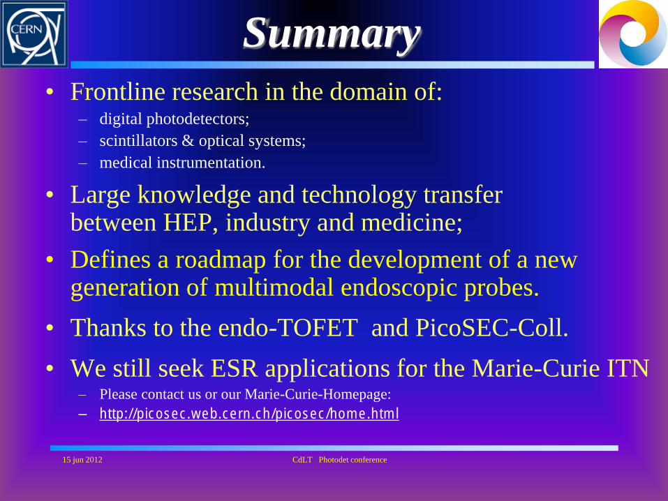
Summary
• Frontline research in the domain of: – digital photodetectors;
– scintillators & optical systems;
– medical instrumentation.
• Large knowledge and technology transfer between HEP, industry and medicine;
• Defines a roadmap for the development of a new generation of multimodal endoscopic probes.
• Thanks to the endo-TOFET and PicoSEC-Coll.
• We still seek ESR applications for the Marie-Curie ITN – Please contact us or our Marie-Curie-Homepage:
– http://picosec.web.cern.ch/picosec/home.html
CdLT Photodet conference 15 jun 2012

15 jun 2012 CdLT Photodet conference
Semiconductor roadmap (detail 2008-10)
MOS Capacity by Dimensions
0,0
400,0
800,0
1200,0
1600,0
2000,0
2400,0
1Q
08
2Q
08
3Q
08
4Q
08
1Q
09
2Q
09
3Q
09
4Q
09
1Q
10
2Q
10
3Q
10
4Q
10
WS
pW
x1
00
0
>=0.7µ
<0.7µ >=0.4µ
<0.4µ >=0.2µ
<0.2µ >=0.12µ
<0.12µ >=0.08µ
<0.08µ
<0.08>=0.06µ
<0.06

15 jun 2012 CdLT Photodet conference
Readout electronics : requirements
Low
cost ! (and even less)
Radiation
hardness
High
reliabilit
y
High
speed
Large
dynamic
range
Low
power
Low
material
Low
noise

15 jun 2012 CdLT Photodet conference
MOS and Bipolar
http://cmp.imag.fr/aboutus/slides/Slides2011/02_Runs_2011.pdf
© K. Troki (CMP)

15 jun 2012 CdLT Photodet conference
© K. Troki (CMP)

New R&D developments: PETIROC
CdLT Photodet conference
• SiPM readout in 0.35µm SiGe, for TOF PET MRI and pre clinical applications,
• 12 channels with 3 different architectures (end of 2011)
• High bandwidth preamp (GBWP> 10 GHz), <3 mW/ch, internal TDC (step=25 ps)
• Dual time and charge measurement up to 2500 pe-

Performance
• Good testbench performance: jitter < 10 ps rms
• Patented input stage for dual time and charge measurement
• Strong industrial interest
• Test boards with bonded die available for academic applications
• 16 channels chip to be submitted
CdLT Photodet conference
• Startup Weeroc http://weeroc.com/ created from OMEGA
for industrial applications contact person: Julien Fleury
CdLT Photodet conference
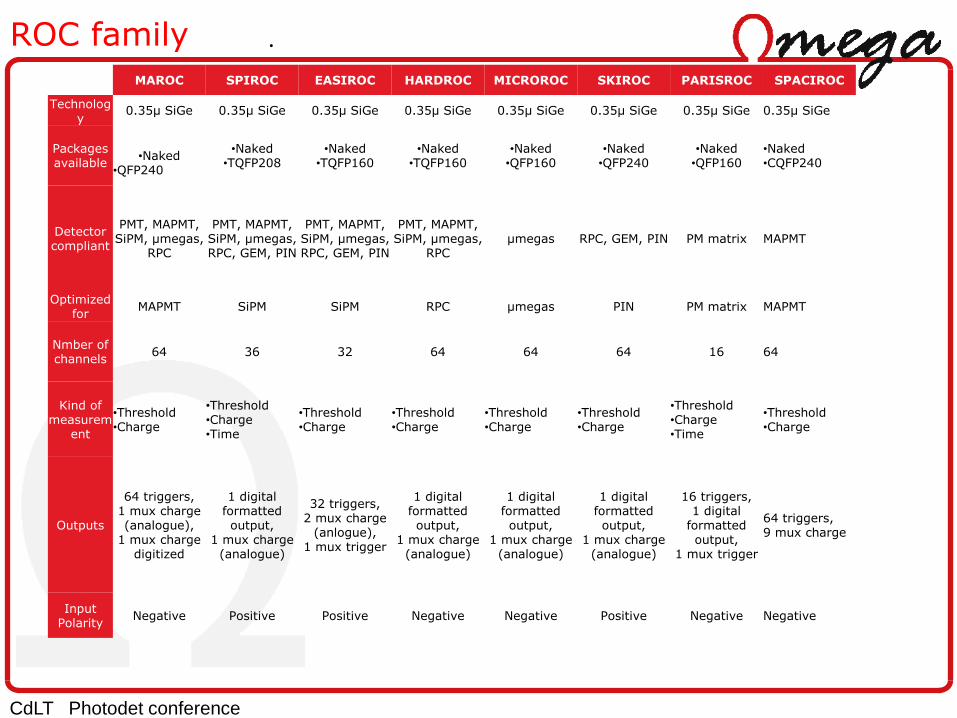
ROC family
MAROC SPIROC EASIROC HARDROC MICROROC SKIROC PARISROC SPACIROC
Technology
0.35µ SiGe 0.35µ SiGe 0.35µ SiGe 0.35µ SiGe 0.35µ SiGe 0.35µ SiGe 0.35µ SiGe 0.35µ SiGe
Packages available
•Naked
•QFP240
•Naked •TQFP208
•Naked •TQFP160
•Naked •TQFP160
•Naked •QFP160
•Naked •QFP240
•Naked •QFP160
•Naked •CQFP240
Detector compliant
PMT, MAPMT, SiPM, µmegas,
RPC
PMT, MAPMT, SiPM, µmegas, RPC, GEM, PIN
PMT, MAPMT, SiPM, µmegas, RPC, GEM, PIN
PMT, MAPMT, SiPM, µmegas,
RPC µmegas RPC, GEM, PIN PM matrix MAPMT
Optimized for
MAPMT SiPM SiPM RPC µmegas PIN PM matrix MAPMT
Nmber of channels
64 36 32 64 64 64 16 64
Kind of measurem
ent
•Threshold •Charge
•Threshold •Charge •Time
•Threshold •Charge
•Threshold •Charge
•Threshold •Charge
•Threshold •Charge
•Threshold •Charge •Time
•Threshold •Charge
Outputs
64 triggers, 1 mux charge (analogue),
1 mux charge digitized
1 digital formatted output,
1 mux charge (analogue)
32 triggers, 2 mux charge
(anlogue), 1 mux trigger
1 digital formatted output,
1 mux charge (analogue)
1 digital formatted output,
1 mux charge (analogue)
1 digital formatted output,
1 mux charge (analogue)
16 triggers, 1 digital
formatted output,
1 mux trigger
64 triggers, 9 mux charge
Input Polarity
Negative Positive Positive Negative Negative Positive Negative Negative
•

Measurements of SiPM in coincidence with a PMT (II)
Timing accuracy of the fast-OR signal vs
the trigger provided by the PMT
Low threshold level:
timing accuracy 1.2 ns FWHM
Energy spectrum of 22Na
Threshold increased to get rid of the
Comptons:
energy resolution 11% FWHM
8th International Meeting on Front-End Electronics, May 24-27, 2011, Bergamo
15 jun 2012 CdLT Photodet conference