single-mask double-patterning lithography for reduced...
TRANSCRIPT
1
Single-Mask Double-Patterning Lithography forReduced Cost and Improved Overlay Control
Rani S. Ghaida, George Torres, and Puneet GuptaEE Dept., University of California, Los Angeles
[email protected], [email protected], and [email protected]
Abstract—1 We propose shift-trim double patterning lithogra-phy (ST-DPL), a cost-effective double patterning technique forachieving pitch relaxation with a single photomask. The maskis re-used for the second exposure by applying a translationalmask-shift. An additional non-critical trim exposure is appliedto remove extra printed features. ST-DPL can be used to patterncritical layers and is very suitable for regular and griddedlayouts, where redesign effort and area overhead are minimal.In this paper, the viability of ST-DPL is demonstrated througha design implementation at the poly and contacts layers inbidirectional layouts. Standard-cell layouts are constructed so asto avoid layout decomposition conflicts, which are found to be thelimiting factor for the pitch relaxation that can be achieved withdouble-patterning (ST-DPL as well as standard DPL). 2× pitchrelaxation being associated with a considerable area overhead,1.8× pitch relaxation is achieved in our implementation whileensuring no layout decomposition conflicts and a small areaoverhead. Specifically, in comparison to layouts assumed to befeasible with a hypothetical single-patterning process, we observevirtually no area overhead when ST-DPL is applied to the polylayer (<0.3% cell-area overhead) and no more than 4.7% cell-area overhead when ST-DPL is applied at both the poly andcontacts layers. The proposed method has many benefits overstandard pitch-split double-patterning: (1) cuts mask-cost tonearly half, (2) reduces overlay errors between the two patterns,(3) alleviates the bimodal line-width distribution problem indouble patterning, and (4) slightly enhances the throughput ofcritical-layer scanners.
Index Terms—Double patterning, shift-trim, photomask, trimexposure, overlay, bimodal CD distribution, manufacturingthroughput, mask cost.
I. INTRODUCTION
Double-patterning lithography (DPL) is one of the most likelyshort-term solutions for keeping the pace of scaling beyond32nm node [2]. It is one of the many resolution enhancementtechniques (RET) that have been introduced to push the limitof optical lithography. DPL can be implemented with differentmanufacturing processes: litho-etch-litho-etch (LELE), litho-litho-etch (LLE), and self-aligned double patterning (SADP),a.k.a. spacer double patterning (SDP). In SADP, sidewallspacer defines either spaces or lines depending on the toneof the process and extra printed features are trimmed awayusing a cut or block mask. Many patterns cannot be printedusing SADP, which make it more suitable for well-structuredmemory cells than random logic layout [2]. This paper focuseson LELE and LLE processes referred to as standard-DPLprocesses hereafter.
1This is an extended version of paper [1].
DPL has four major impediments: high mask-cost, lowthroughput, within-layer overlay errors, and the CD bimodalityproblem. DPL mask-cost is estimated to twice that of singlepatterning because of the need for two critical masks. Theadditional processing steps required for double patterningsignificantly reduce the fabrication throughput. The overlaybudget being determined by interactions between different lay-ers in single patterning (e.g., metal overhang on via), 20% ofhalf-pitch estimated by ITRS is considered sufficient. In DPLhowever, overlay budget is much tighter since overlay trans-lates directly into CD variability [3], which has a budget threetimes tighter than inter-layer overlay according to ITRS [4],and, hence, introduces an extra source of variability [5]. CDtypically follows a normal distribution with some σ and µ,which deviates slightly from the target. Since DPL has twoseparate exposure and etch steps, two populations exist: onefor features formed by the first exposure/etch step and anotherfor features formed by the second exposure/etch step.
An attempt to use DPL with a single photomask and, hence,reduce its cost, is reported in [6]. It consists of splitting themask area into two regions, each corresponding to a differentpattern (similar to a multi-layer reticle). As reported in [6], thisapproach renders fabrication throughput even worse than thatof standard-DPL and does not address other DPL technicalchallenges including within-layer overlay and CD bimodality.
In this paper, we extend our work presented in [1]. In partic-ular, we propose shift-trim DPL (ST-DPL), an effective methodto use a single mask to achieve pitch-relaxation. Essentially,the method consists of applying a translational mask-shift tore-use the same photomask for both exposures of DPL. Extraprinted features are then removed using a non-critical trimexposure. ST-DPL can be applied to all layers including, butnot limited to, active, polysilicon, contacts, metal, and vialayers. Moreover, the method can be used for any type ofdesign as long as some basic layout restrictions (discussedin Section III) are met. In this paper, we demonstrate theviability of the proposed method when employed to patternthe polysilicon (poly) and contacts (CA) layers in standard-cell based designs. Cell layouts are constructed so that to avoidlayout decomposition conflicts. Resolving decomposition con-flicts between features of different cells is found to be thelimiting factor for the pitch relaxation that can be achievedwith double patterning (ST-DPL as well as standard DPL).As a result, 2× pitch relaxation without conflicts is achievedonly at high area overhead. ST-DPL designs show little areaoverhead, however, while ensuring 1.8× pitch relaxation andno layout decomposition conflicts.
2
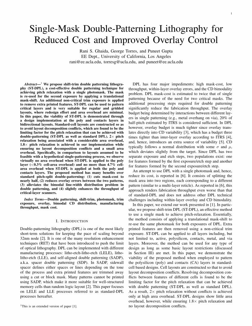
Figure 1. Proposed manufacturing processes for ST-DPL: positive dual-line and negative dual-trench LELE, positive dual-line LLE, a.k.a. litho-freeze-litho-etch(LFLE) process, and negative dual-trench double-exposure processes.
ST-DPL manufacturing process and design requirements arediscussed in Section II. In Section III, ST-DPL feasibility at thepoly and CA layers are demonstrated by creating a compatiblestandard-cell library by layout migration of Nangate opencell-library [7] and generating compatible real designs. Whencompared to the original Nangate layouts (assumed to befeasible with a hypothetical single-patterning process), ST-DPL designs show virtually no area overhead for ST-DPLimplementation at the poly layer and an affordable areaoverhead of at most 4.7% for ST-DPL implementation at boththe poly and CA layers. In both ST-DPL implementations, thegenerated trim mask layouts are simple and lead to an easy-to-fabricate photomask. Benefits of the proposed method in termsof cost, overlay control, CD performance, and throughput arediscussed in Section IV, while Section V concludes with asummary.
II. SHIFT-TRIM DPL OVERVIEW AND LAYOUTRESTRICTIONS
This section presents an overview of ST-DPL technique andits associated layout restrictions and challenges.
A. Manufacturing ProcessST-DPL involves the following steps:1. print the first pattern as in standard DPL processes;2. shift the photomask of step (1) by a predetermined
nanoscale amount X (equal to minimum gate pitch forpoly-layer ST-DPL) and print the second pattern;
3. apply a non-critical trim (a.k.a. block) exposure toremove unnecessary features.
The translational mask shift in step (2) is accomplishedwithout any unloading and reloading of the photomask fromthe exposure tool and no extra requirements on exposure tools.Today’s scanners have the capability to perform such transla-tional shift automatically with high precision (≈ 0.6nm) [8].
ST-DPL can be implemented using positive dual-line andnegative dual-trench LELE and LLE processes with littlemodifications as demonstrated in Figure 12. We only showthe case of positive resist since it is more commonly usedin modern lithography. Negative resist can also be used withlittle changes to the manufacturing process. In this figure, theprocesses are presented in order of popularity with the firstprocess on the left being the most popular. Although LLE hashigher throughput and lower cost than LELE, to best of ourknowledge, LLE is currently not production-worthy. For ourdesign implementation of ST-DPL, we use a positive dual-lineLELE process. Nevertheless, ST-DPL implementation with theother less popular/realistic alternatives can be performed withlittle modifications.
ST-DPL requires an extra step on top of standard-DPL.It consists of an inexpensive and non-critical trim-exposurecycle (resist coat-expose-develop) and removal of hardmaskcorresponding to extra printed features before the final etch.The trim exposure is a mature and well-known method usedin many patterning techniques such as SADP [9, 10], alter-nating phase-shift mask [11], and subtractive-litho pattern-ing [12, 13]. It was recently employed to trim-away printing
3
assist features (PrAF) introduced to enhance the resolution ofconventional single patterning [14]. A second hardmask layeris necessary in case of positive LELE process, but this doesnot represent an extra requirement because many standard DPLimplementations favor the use of a second hardmask [3, 15].Relaxed CD and overlay requirements of the trim exposure,which are demonstrated by the results of our implementation,make process control an easy task. Consequently, the costof trim mask is minor compared to the cost of conventionalmasks and the trim exposure can be realized using second-tierscanners if this is desirable to enhance throughput.
B. ST-DPL Challenges and DownsidesIn addition to the downside of the need for three exposures
(two critical and one non-critical trim exposure) and the extraprocessing steps associated with the trim exposure, ST-DPLhas two other challenges.
Although the same features with exactly the same sur-roundings are on the mask of the first and second exposures,features of different exposures printed on wafer may vary dueto process-differences (e.g., resist thickness, hardmask charac-teristics, etch-interference, etc...). One way to compensate forthis difference consists of using different OPC features for thedifferent patterns [16]. In ST-DPL, this method is no longerpossible since the same mask is used for the first and secondexposures. As a result, other means to correct for processingdifferences between the two patterns must be employed (e.g.,dose-mapping [17]).
Because the ST-DPL mask-shift is performed just uniformlyacross the design, the minimum gate-pitch must be set tothe contacted gate-pitch (typically equal to the amount ofthe mask-shift) and all gates in the design must follow thesame orientation. When memory and logic are integrated, thisgate-pitch limitation may impose restrictions on the allowedcontacted pitch for memory if it is not the same as the logiccontacted pitch.
C. Layout Restrictions at Poly-line LayerBasic layout restrictions are imposed for implementing ST-
DPL at the poly layer. X being the amount of mask shift andX0 being the minimum gate pitch on the mask3, the followingrestrictions apply.
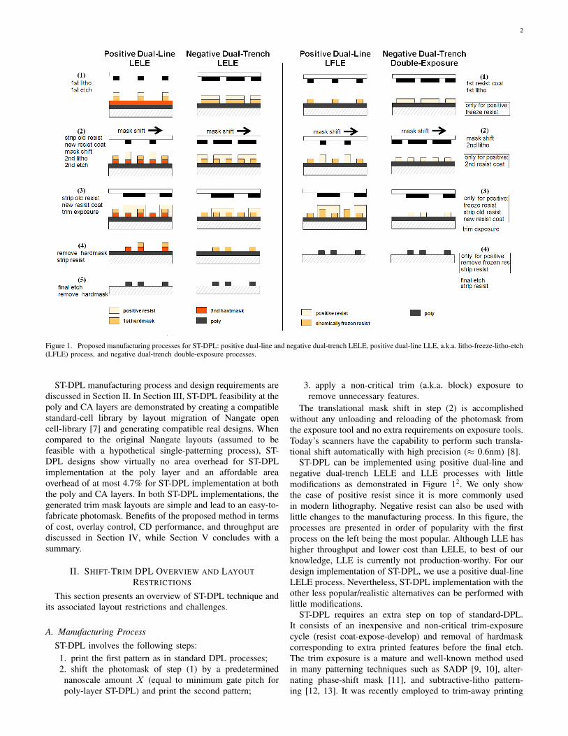
1. For every gate, the pitch to the neighboring gates fromone side (subsequent gate to the right or left side) must beeither X or ≥ X0 and the pitch between the left and rightneighboring gates must be ≥ X0. This is illustrated bythe example of three gate-poly lines shown in Figure 2.
2. In light of (1), minimum gate spacing is equal tocontacted-gate spacing (equal to X minus poly-linewidth).
3. “Wrong-direction” (horizontal) poly routing is re-stricted to top and bottom routing channels of the cell(i.e. poly-routing in the center of the cell is not allowed).
In addition, some design rule restrictions (especially line-end to field-poly spacing and line-end gap) may be necessaryto guarantee a simple trim-mask as we show later in this paper.
2BARC layers are not shown for brevity.
Figure 2. Example illustrating gate-pitch restriction. In case Pitch(AB) is< X0 but different than X , then Pitch(BC) must be either X or ≥ X0
and Pitch(AC) must be ≥ X0. Similarly, if Pitch(BC) is unrestricted,Pitch(AB) is restricted to X or ≥ X0 and Pitch(AC) to ≥ X0.
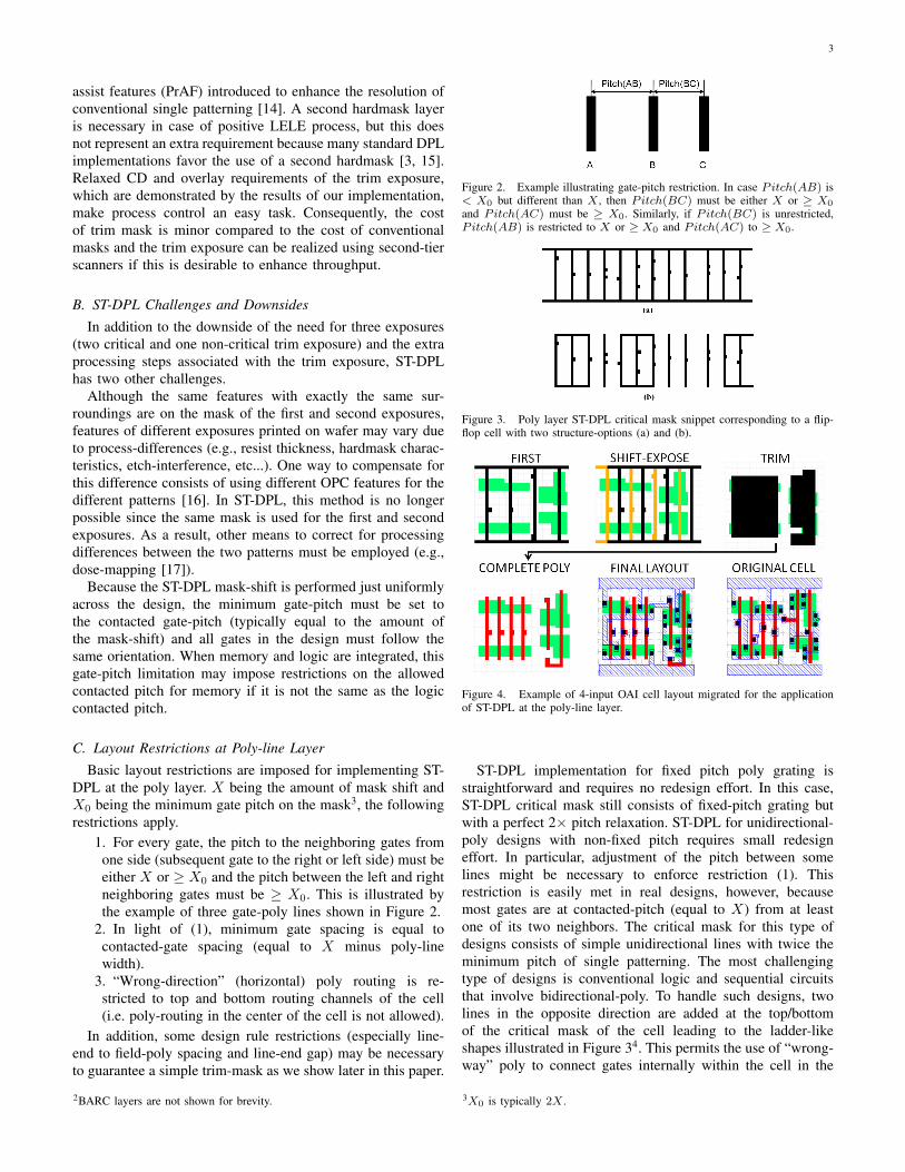
Figure 3. Poly layer ST-DPL critical mask snippet corresponding to a flip-flop cell with two structure-options (a) and (b).
Figure 4. Example of 4-input OAI cell layout migrated for the applicationof ST-DPL at the poly-line layer.
ST-DPL implementation for fixed pitch poly grating isstraightforward and requires no redesign effort. In this case,ST-DPL critical mask still consists of fixed-pitch grating butwith a perfect 2× pitch relaxation. ST-DPL for unidirectional-poly designs with non-fixed pitch requires small redesigneffort. In particular, adjustment of the pitch between somelines might be necessary to enforce restriction (1). Thisrestriction is easily met in real designs, however, becausemost gates are at contacted-pitch (equal to X) from at leastone of its two neighbors. The critical mask for this type ofdesigns consists of simple unidirectional lines with twice theminimum pitch of single patterning. The most challengingtype of designs is conventional logic and sequential circuitsthat involve bidirectional-poly. To handle such designs, twolines in the opposite direction are added at the top/bottomof the critical mask of the cell leading to the ladder-likeshapes illustrated in Figure 34. This permits the use of “wrong-way” poly to connect gates internally within the cell in the
3X0 is typically 2X .
4
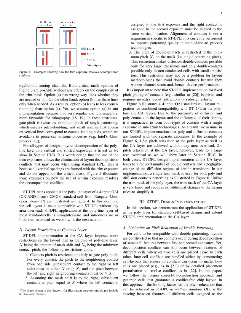
Figure 5. Examples showing how the trim exposure resolves decompositionconflicts.
top/bottom routing channels. Both critical-mask options ofFigure 3 are possible without any effects on the complexity ofthe trim-mask. Option (a) has wrong-way lines whether theyare needed or not. On the other hand, option (b) has these linesonly when needed. As a results, option (b) leads to less corner-rounding than option (a). Yet, we assume option (a) in ourimplementation because it is very regular and, consequently,more favorable for lithography [18, 19]. In these structures,gate-pitch is twice the minimum pitch of single patterning,which ensures pitch-doubling, and small notches that appearon vertical lines correspond to contact-landing pads, which areavoidable in processes in some processes (e.g. Intel’s 45nmprocess [12]).
For all types of designs, layout decomposition of the poly-line layer into critical and shifted exposures is trivial as weshow in Section III-B. It is worth noting that the use of thetrim exposures allows the elimination of layout decompositionconflicts that may occur when using standard DPL. This isbecause all vertical spacings are formed with the trim exposureand do not appear on the critical mask. Figure 5 illustratessome examples on how the use of a trim exposure resolvesthe decomposition conflicts.
ST-DPL steps applied at the poly-line layer of a 4-input OAI(OR-AND-Invert) CMOS standard-cell from Nangate 45nmopen library [7] are illustrated in Figure 4. In this example,the cell-layout is made compatible with ST-DPL without anyarea overhead. ST-DPL application at the poly-line layer ofmost standard-cells is straightforward and introduces no orlittle area overhead as we show in the next section.
D. Layout Restrictions at Contacts LayerST-DPL implementation at the CA layer imposes more
restrictions on the layout than in the case of poly-line layer.X being the amount of mask shift and X0 being the minimumcontact pitch, the following restrictions apply.
1. Contacts pitch is restricted similarly to gate-poly pitch.For every contact, the pitch to the neighboring contactfrom one side (subsequent contact to the right or leftside) must be either X or ≥ X0 and the pitch betweenthe left and right neighboring contacts must be ≥ X0.
2. Assuming the mask shift is to the right, subsequentcontacts at pitch equal to X where the left contact is
4The shape shown in this figure is for illustration purposes and do not includeRET-related features.
assigned to the first exposure and the right contact isassigned to the second exposure must be aligned to thesame vertical location. Alignment of contacts is not arequirement specific to ST-DPL; it is currently performedto improve patterning quality in state-of-the-art processtechnologies.
3. The pitch of double-contacts is restricted to the mini-mum pitch X0 on the mask (i.e. single-patterning pitch).This restriction makes diffusion double-contacts possibleonly for very large transistors and poly double-contactspossible only in non-condensed cells with small transis-tors. This restriction may not be a problem for layoutmethodologies that avoid double contacts because theyworsen channel strain and, hence, device performance.
It is important to note that ST-DPL implementation for fixedpitch grating of contacts (e.g., similar to [20]) is trivial andrequires no extra layout restrictions or redesign efforts.
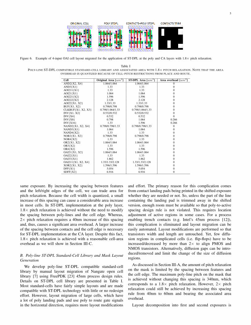
Figure 6 illustrates a 4-input OAI standard-cell layout mi-gration for combined compatibility with ST-DPL at the poly-line and CA layers. Due to the proximity of diffusion andpoly contacts in the layout and the difference of their depths,it is impractical to form both types of contacts with a singleexposure in sub-32nm technologies. As a result, we assume inour ST-DPL implementation that poly and diffusion contactsare formed with two separate exposures. In the example ofFigure 6, 1.8× pitch relaxation at the poly layer as well asthe CA layer are achieved without any area overhead. 2×pitch relaxation at the CA layer, however, leads to a largearea overhead as we will show later in Section III-C. Inboth cases, ST-DPL design implementation at the CA layerleads to a reduced number of double contacts and a negligiblechange of the diffusion regions of certain transistors. In ourimplementation, a single trim mask is used for both poly anddiffusion contacts patterning as illustrated in Figure 6. Unlikethe trim mask of the poly layer, the trim mask of the CA layeris very basic and requires no additional changes to the designrules to simplify it.
III. STDPL DESIGN IMPLEMENTATION
In this section, we demonstrate the application of ST-DPLat the poly layer for standard cell-based designs and extendST-DPL implementation to the CA layer.
A. Limitation on Pitch Relaxation of Double PatterningFor cells to be compatible with double patterning, layouts
are constructed so that no conflicts occur during decompositionof same-cell features between first and second exposures. Yet,decomposition conflicts can still occur between features ofdifferent cells whenever two cells are placed close to eachother. Inter-cell conflicts are handled either by constructingcell-layouts that ensure no conflicts can occur no matter howcells are placed (e.g., as in [21]) or by detailed placementperturbation to resolve conflicts as in [22]. In this paper,we follow the former correct-by-construction approach andgenerate cells that guarantee a conflict-free chip layout. Inthis approach, the limiting factor for the pitch relaxation thatcan be achieved in ST-DPL as well as standard DPL is thespacing between features of different cells assigned to the
5
Figure 6. Example of 4-input OAI cell layout migrated for the application of ST-DPL at the poly and CA layers with 1.8× pitch relaxation.
Table IPOLY-LINE ST-DPL COMPATIBLE STANDARD-CELL LIBRARY AND ASSOCIATED AREA WITH 1.8× PITCH RELAXATION. NOTE THAT THE AREA
OVERHEAD IS QUANTIZED BECAUSE OF CELL-PITCH RESTRICTIONS FROM PLACE AND ROUTE.
Cell Original Area [um2] ST-DPL Area [um2] Area overhead [um2]AND2{X2, X4} 1.064/1.064 1.064/1.064 0AND3{X1} 1.33 1.33 0AOI211{X1} 1.33 1.33 0AOI21{X1} 1.064 1.064 0AOI221{X2} 1.596 1.596 0AOI222{X2} 2.128 2.128 0AOI22{X1, X2} 1.33/1.33 1.33/1.33 0BUF{X1, X2} 0.798/0.798 0.798/0.798 0CLKBUF{X1, X2, X3} 0.798/1.064/1.33 0.798/1.064/1.33 0INV{X1, X2} 0.532/0.532 0.532/0.532 0INV{X4} 0.532 0.532 0INV{X8} 0.798 1.064 0.266INV{X16} 1.33 1.596 0.266NAND2{X1, X2, X4} 0.798/0.798/1.33 0.798/0.798/1.33 0NAND3{X1} 1.064 1.064 0NAND4{X2} 1.33 1.33 0NOR2{X1, X2} 0.798/0.798 0.798/0.798 0NOR4{X2} 1.33 1.33 0OR2{X1, X2} 1.064/1.064 1.064/1.064 0OR3{X2} 1.33 1.33 0OR4{X2} 1.596 1.596 0OAI21{X1, X2} 1.064/1.064 1.064/1.064 0OAI22{X1} 1.33 1.33 0OAI33{X1} 1.862 1.862 0OAI211{X1, X2, X4} 1.33/1.33/2.128 1.33/1.33/2.128 0XOR2{X1, X2} 1.596/1.596 1.596/1.596 0DFF{X1} 5.054 5.054 0SDFF{X2} 6.916 6.916 0
same exposure. By increasing the spacing between featuresand the left/right edges of the cell, we can trade area forpitch relaxation. Because the cell width is quantized, a smallincrease of this spacing can cause a considerable area increasein most cells. In ST-DPL implementation at the poly layer,1.8× pitch relaxation is achieved without the need to modifythe spacing between poly-lines and the cell edge. Whereas,2× pitch relaxation requires a 40nm increase of this spacingand, thus, causes a significant area overhead. A larger increaseof the spacing between contacts and the cell edge is necessaryfor ST-DPL implementation at the CA layer. Despite this fact,1.8× pitch relaxation is achieved with a reasonable cell-areaoverhead as we will show in Section III-C.
B. Poly-line ST-DPL Standard-Cell Library and Mask LayoutGeneration
We develop poly-line ST-DPL compatible standard-celllibrary by manual layout migration of Nangate open celllibrary [7] using FreePDK [23] 45nm process design rules.Details on ST-DPL cell library are presented in Table I.Most standard-cells have fairly simple layouts and are madecompatible with ST-DPL technology with little or no redesigneffort. However, layout migration of large cells, which havea lot of poly landing pads and use poly to route gate signalsin the horizontal direction, requires more layout modifications
and effort. The primary reason for this complication comesfrom contact landing pads being printed in the shifted exposurewhether they are needed or not. So, unless the part of the linecontaining the landing pad is trimmed away in the shiftedversion, enough room must be available so that poly-to-activespacing design rule is not violated. This requires locationadjustment of active regions in some cases. For a processenabling trench contacts (e.g. Intel’s 45nm process [12]),this complication is eliminated and layout migration can beeasily automated. Layout modifications are performed so thattransistors width and length are untouched. Yet, few diffu-sion regions in complicated cells (i.e. flip-flops) have to beincreased/decreased by more than 2× to align PMOS andNMOS transistors. Alternatively, diffusion gaps can be intro-duced/removed and limit the change of the size of diffusionregions.
As discussed in Section III-A, the amount of pitch relaxationon the mask is limited by the spacing between features andthe cell edge. The maximum poly-line pitch on the mask thatis achieved without changing this spacing is 340nm, whichcorresponds to a 1.8× pitch relaxation. However, 2× pitchrelaxation could still be achieved by increasing this spacingrule from 40nm to 60nm and bearing the associated areaoverhead.
Layout decomposition into first and second exposures is
6
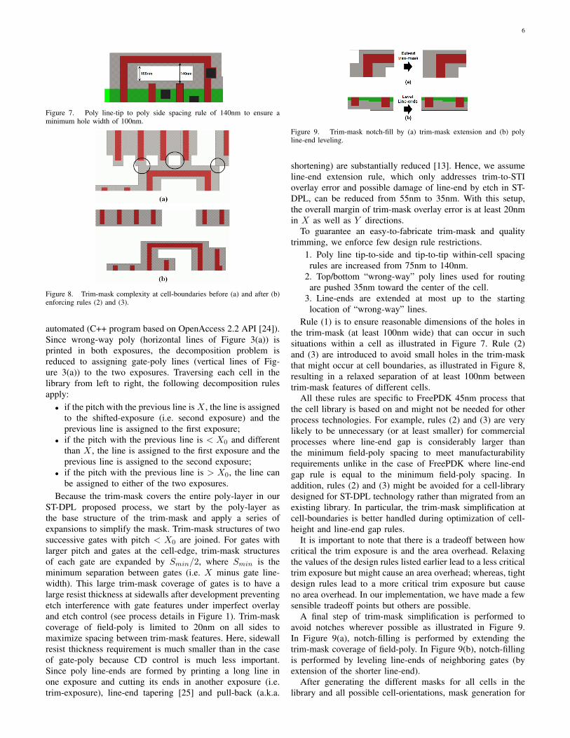
Figure 7. Poly line-tip to poly side spacing rule of 140nm to ensure aminimum hole width of 100nm.
Figure 8. Trim-mask complexity at cell-boundaries before (a) and after (b)enforcing rules (2) and (3).
automated (C++ program based on OpenAccess 2.2 API [24]).Since wrong-way poly (horizontal lines of Figure 3(a)) isprinted in both exposures, the decomposition problem isreduced to assigning gate-poly lines (vertical lines of Fig-ure 3(a)) to the two exposures. Traversing each cell in thelibrary from left to right, the following decomposition rulesapply:
• if the pitch with the previous line is X , the line is assignedto the shifted-exposure (i.e. second exposure) and theprevious line is assigned to the first exposure;
• if the pitch with the previous line is < X0 and differentthan X , the line is assigned to the first exposure and theprevious line is assigned to the second exposure;
• if the pitch with the previous line is > X0, the line canbe assigned to either of the two exposures.
Because the trim-mask covers the entire poly-layer in ourST-DPL proposed process, we start by the poly-layer asthe base structure of the trim-mask and apply a series ofexpansions to simplify the mask. Trim-mask structures of twosuccessive gates with pitch < X0 are joined. For gates withlarger pitch and gates at the cell-edge, trim-mask structuresof each gate are expanded by Smin/2, where Smin is theminimum separation between gates (i.e. X minus gate line-width). This large trim-mask coverage of gates is to have alarge resist thickness at sidewalls after development preventingetch interference with gate features under imperfect overlayand etch control (see process details in Figure 1). Trim-maskcoverage of field-poly is limited to 20nm on all sides tomaximize spacing between trim-mask features. Here, sidewallresist thickness requirement is much smaller than in the caseof gate-poly because CD control is much less important.Since poly line-ends are formed by printing a long line inone exposure and cutting its ends in another exposure (i.e.trim-exposure), line-end tapering [25] and pull-back (a.k.a.
Figure 9. Trim-mask notch-fill by (a) trim-mask extension and (b) polyline-end leveling.
shortening) are substantially reduced [13]. Hence, we assumeline-end extension rule, which only addresses trim-to-STIoverlay error and possible damage of line-end by etch in ST-DPL, can be reduced from 55nm to 35nm. With this setup,the overall margin of trim-mask overlay error is at least 20nmin X as well as Y directions.
To guarantee an easy-to-fabricate trim-mask and qualitytrimming, we enforce few design rule restrictions.
1. Poly line tip-to-side and tip-to-tip within-cell spacingrules are increased from 75nm to 140nm.
2. Top/bottom “wrong-way” poly lines used for routingare pushed 35nm toward the center of the cell.
3. Line-ends are extended at most up to the startinglocation of “wrong-way” lines.
Rule (1) is to ensure reasonable dimensions of the holes inthe trim-mask (at least 100nm wide) that can occur in suchsituations within a cell as illustrated in Figure 7. Rule (2)and (3) are introduced to avoid small holes in the trim-maskthat might occur at cell boundaries, as illustrated in Figure 8,resulting in a relaxed separation of at least 100nm betweentrim-mask features of different cells.
All these rules are specific to FreePDK 45nm process thatthe cell library is based on and might not be needed for otherprocess technologies. For example, rules (2) and (3) are verylikely to be unnecessary (or at least smaller) for commercialprocesses where line-end gap is considerably larger thanthe minimum field-poly spacing to meet manufacturabilityrequirements unlike in the case of FreePDK where line-endgap rule is equal to the minimum field-poly spacing. Inaddition, rules (2) and (3) might be avoided for a cell-librarydesigned for ST-DPL technology rather than migrated from anexisting library. In particular, the trim-mask simplification atcell-boundaries is better handled during optimization of cell-height and line-end gap rules.
It is important to note that there is a tradeoff between howcritical the trim exposure is and the area overhead. Relaxingthe values of the design rules listed earlier lead to a less criticaltrim exposure but might cause an area overhead; whereas, tightdesign rules lead to a more critical trim exposure but causeno area overhead. In our implementation, we have made a fewsensible tradeoff points but others are possible.
A final step of trim-mask simplification is performed toavoid notches wherever possible as illustrated in Figure 9.In Figure 9(a), notch-filling is performed by extending thetrim-mask coverage of field-poly. In Figure 9(b), notch-fillingis performed by leveling line-ends of neighboring gates (byextension of the shorter line-end).
After generating the different masks for all cells in thelibrary and all possible cell-orientations, mask generation for
7
Table IIDETAILS OF POLY-LINE ST-DPL COMPATIBLE DESIGNS SHOWING NEGLIGIBLE AREA OVERHEAD.
Description Cell instances Cell-types Flip-flops INV/BUF Cell-area [um2] Area overheadmips789 processor core 10529 35 2011 1465 22867.5 0.02%or1200 combinational logic 3070 35 0 890 3014.8 0.34%usb com. controller 478 31 93 52 880.2 0%
(a) (b)
Figure 10. Trim-mask layout snippet for poly-lines (a) and contacts (b). In (a), simple large blocks correspond to cells with unidirectional poly-lines andmore complex shapes correspond to flip-flops with bidirectional poly-routing. In (b), both flip-flop and combinational logic regions have simple trim-maskfeatures.
Table IIIDETAILS ON TRIM-MASK AT THE POLY-LINE LAYER FOR THE DESIGN OF TABLE II SHOWING VERY BASIC FABRICATION REQUIREMENTS.
Line-width Notch Hole Overlay Trim-mask Post-OPC[nm] Size [nm] dimensions [nm] margin [nm] fractures poly fractures
MIPS789 ≥ 90 ≥ 70 ≥ 190 x 145 20 78597 367633OR1200 ≥ 90 ≥ 70 ≥ 380 x 100 20 5189 43150USB ≥ 90 ≥ 70 ≥ 190 x 145 20 2770 14404
ST-DPL compatible designs is a simple step. For each cell-instance, cell-type and orientation are determined and mask-features are copied from the corresponding cell in the libraryto the instance location in the design. The generated masklayout is free of errors at cell-boundaries because critical-mask features outside the cell (or close to the cell-edge) aretrimmed away and enough spacing between trim-mask featuresof different cells is guaranteed by construction.
Poly-line ST-DPL standard-cell library is implemented with1.8× pitch relaxation and no area overhead compared to theoriginal Nangate library layouts except for three cells as shownin Table I. This overhead is caused by layout restrictionsimposed to simplify the trim-mask. In case these restrictionsare avoided for the reasons discussed earlier, none of the ST-DPL compatible cells will have any area overhead. Moreover,if option(b) of Figure 3 is used instead of option(a), i.e.having “wrong-way” poly tracks only when needed, ST-DPLimplementation of these three inverter-cells results in no areaoverhead because rule (2) can be avoided.
Three designs from [26] are synthesized in Cadence RTLCompiler TMv6.2 using the developed poly-line ST-DPLstandard-cell library. Designs are placed and routed usingCadence SOC Encounter TMv6.2. Details on the designs andassociated cell-area overhead are presented in Table II. Cell-area overhead for all three designs is negligible (at most0.34%). The reason is attributed to low utilization of thecells where area overhead occurs (low utilization of large-sizeinverters is typical).
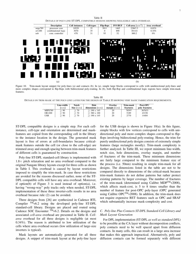
Mask layouts are automatically generated for all threedesigns. A snippet of trim-mask layout at the poly-line layer
for the USB design is shown in Figure 10(a). In this figure,simple blocks with few vertices correspond to cells with uni-directional poly and more complex shapes correspond to flip-flops involving bidirectional poly-routing. Hence, the trim forpurely unidirectional poly designs consists of extremely simplefeatures (large rectangles mostly). Trim-mask complexity isfurther analyzed. In Table III, we report minimum line-width,notch size, hole dimensions, overlay margin, and numberof fractures of the trim-mask. These minimum dimensionsare fairly large compared to the minimum feature size ofthe process (i.e. 50nm) resulting in simple trim-mask for alldesigns. The dimensions listed in the table are not to becompared directly to dimensions of the critical-mask becausetrim-mask features do not define patterns but rather protectexisting patterns by larger coverage. The number of fracturesof the trim-mask (determined using Calibre MDPTMv2008),which affects mask-cost, is 5 to 8 times smaller than thenumber of feature for post-OPC poly-layer (OPC generatedusing Calibre OPCTMv2008). In addition, the trim-mask doesnot require expensive RET features such as OPC and SRAFwhich substantially increase mask-complexity and cost.
C. Poly-line Plus Contacts ST-DPL Standard-Cell Library andMask Layout Generation
For DPL implementation (ST-DPL as well as standard DPL)to be possible at the CA layer without decomposition conflicts,poly contacts need to be well spaced apart from diffusioncontacts. In many cells, this can result in a large area increasethat makes this approach impractical. Alternatively, poly anddiffusion contacts can be formed separately with different
8
Table IVPOLY-LINE PLUS CA ST-DPL COMPATIBLE STANDARD-CELL LIBRARY AND ASSOCIATED AREA (IN [um2]) WITH 1.8× PITCH RELAXATION. NOTE THAT
THE AREA OVERHEAD IS QUANTIZED DUE TO CELL-PITCH RESTRICTIONS FROM PLACE AND ROUTE.
Original Poly ST-DPL Poly+CA ST-DPL Poly+Hybrid CA ST-DPLArea Area Overhead Area Overhead Area Overhead
AND2{X2} 1.064 1.064 0 1.064 0 1.064 0BUF{X2} 0.798 0.798 0 1.064 0.266 0.798 0CLKBUF{X2} 1.064 1.064 0 1.064 0 1.064 0INV{X2} 0.532 0.532 0 0.532 0 0.532 0INV{X4} 0.532 0.532 0 0.532 0 0.532 0NAND2{X2} 0.798 0.798 0 1.064 0.266 0.798 0NOR2{X2} 0.798 0.798 0 1.064 0.266 0.798 0OR2{X2} 1.064 1.064 0 1.064 0 1.064 0OAI211{X4} 2.128 2.128 0 2.128 0 2.128 0XOR2{X1} 1.596 1.596 0 1.596 0 1.596 0DFF{X1} 5.054 5.054 0 5.586 0.532 5.586 0.532SDFF{X2} 6.916 6.916 0 6.916 0 6.916 0
Table VCELL-AREA (IN [um2]) OF THREE DESIGNS SYNTHESIZED USING POLY PLUS CA ST-DPL COMPATIBLE CELLS FOR THE DIFFERENT SCHEMES.
Original Poly ST-DPL Poly+CA ST-DPL Poly+Hybrid CA ST-DPLCell instances Cell-types Flip-flops INV/BUF Area Area Overhead Area Overhead Area Overhead
MIPS789 20192 12 2011 3878 29733 29733 0% 33289 12% 29931 0.7%OR1200 4240 10 0 889 3759 3759 0% 4436 18% 3759 0%USB 674 10 93 49 1011 1011 0% 1154 14.2% 1058 4.7%
(a) (b)
Figure 11. Example of layout decomposition conflicts (marked with thearrows) between features of different cells (a) and our correct-by-constructioncell layout that guarantees no conflicts (b).
exposures. In addition to the area benefit, the latter approachhas improved printability because the process can be optimizedseparately for each type of contacts that have different depthsand may even have different shapes and dimensions. The latterapproach is assumed in our implementation.
As discussed in Section III-A, to resolve inter-cell layoutdecomposition conflicts and generate correct-by-constructioncell layouts, the spacing between features and the cell edgeneed to be increased. In case of contacts, this increase is largebecause contacts can be placed very near the cell edge. Toreduce the associated area overhead, we perform the followingstrategy. We assign the leftmost features in every cell (includ-ing cells flipped during placement) to the first exposure. Inthis way, when abutting two cells side by side, decompositionconflicts can occur only if the rightmost contacts of the left cellis assigned to the first exposure as illustrated in Figure 11(a).Therefore, only for those particular cells, the spacing betweenthe rightmost contacts and the right edge of the cell need tobe increased as shown in Figure 11(b). The amount of thisincrease to achieve 1.8× pitch relaxation (345nm pitch) at theCA layer is 190nm (or a single cell-width unit in FreePDKdesign rules).
In ST-DPL implementation at the contacts layer, diffusion
contacts are the principal cause of area overhead due to theirproximity to the cell edge. To deal with this issue, we introducehybrid ST-DPL method as a workaround. Only for cells withthe rightmost diffusion contacts assigned originally to the firstexposure, the method consists of assigning these contacts tobe patterned with the poly contacts in a separate exposure.Consequently, no cell will have the rightmost contacts assignedto the first exposure and there is no need to increase thespacing between diffusion contacts and the cell edge as in theoriginal CA ST-DPL implementation. It is also worth notingthat, by preventing the placement of poly contacts betweenthe horizontal location of the first/last gate and the cell edge,ST-DPL can be safely employed to form poly contacts withoutcausing any area overhead.
For the two different styles (ST-DPL and hybrid ST-DPL),we construct a small set of compatible cells by manuallayout migration of poly-line ST-DPL compatible cells thatwere presented in Section III-B. Table IV summarizes theimplemented cells and the area overhead associated with eachstyle. Unlike ST-DPL at poly-line layer, layout migration forST-DPL implementation at the CA layer is a difficult task. Themain reason for this complication is because contacts that areshifted replica of one another must be perfectly aligned atthe same vertical location and at a pitch equal to the amountof mask shift X . Layout modifications are performed so thattransistors width and length are untouched. Length of diffusionhave to be increased by 5nm to ensure contacts are at adistance equal to X . Double-contacts pitch being restricted tothe single-patterning pitch, double-contacts were not possiblein our ST-DPL design implementation because all cells havesmall transistor sizes.
We synthesize the three designs used in the implementationof ST-DPL at the poly-line layer (shown in II using poly-lineplus CA ST-DPL compatible cells of Table IV. Cell-area ofthe three designs after placement and routing for the differentST-DPL flavors are presented in Table V. Implementation ofST-DPL at poly-line and CA layers (Poly+CA ST-DPL) resultsin 12 to 18% cell-area increase. Whereas, poly-line plus hybrid
9
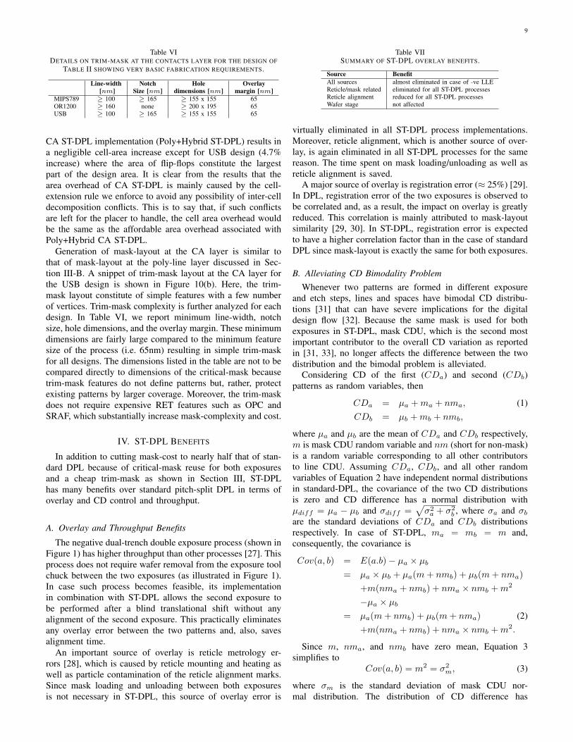
Table VIDETAILS ON TRIM-MASK AT THE CONTACTS LAYER FOR THE DESIGN OF
TABLE II SHOWING VERY BASIC FABRICATION REQUIREMENTS.
Line-width Notch Hole Overlay[nm] Size [nm] dimensions [nm] margin [nm]
MIPS789 ≥ 100 ≥ 165 ≥ 155 x 155 65OR1200 ≥ 160 none ≥ 200 x 195 65USB ≥ 100 ≥ 165 ≥ 155 x 155 65
CA ST-DPL implementation (Poly+Hybrid ST-DPL) results ina negligible cell-area increase except for USB design (4.7%increase) where the area of flip-flops constitute the largestpart of the design area. It is clear from the results that thearea overhead of CA ST-DPL is mainly caused by the cell-extension rule we enforce to avoid any possibility of inter-celldecomposition conflicts. This is to say that, if such conflictsare left for the placer to handle, the cell area overhead wouldbe the same as the affordable area overhead associated withPoly+Hybrid CA ST-DPL.
Generation of mask-layout at the CA layer is similar tothat of mask-layout at the poly-line layer discussed in Sec-tion III-B. A snippet of trim-mask layout at the CA layer forthe USB design is shown in Figure 10(b). Here, the trim-mask layout constitute of simple features with a few numberof vertices. Trim-mask complexity is further analyzed for eachdesign. In Table VI, we report minimum line-width, notchsize, hole dimensions, and the overlay margin. These minimumdimensions are fairly large compared to the minimum featuresize of the process (i.e. 65nm) resulting in simple trim-maskfor all designs. The dimensions listed in the table are not to becompared directly to dimensions of the critical-mask becausetrim-mask features do not define patterns but, rather, protectexisting patterns by larger coverage. Moreover, the trim-maskdoes not require expensive RET features such as OPC andSRAF, which substantially increase mask-complexity and cost.
IV. ST-DPL BENEFITS
In addition to cutting mask-cost to nearly half that of stan-dard DPL because of critical-mask reuse for both exposuresand a cheap trim-mask as shown in Section III, ST-DPLhas many benefits over standard pitch-split DPL in terms ofoverlay and CD control and throughput.
A. Overlay and Throughput Benefits
The negative dual-trench double exposure process (shown inFigure 1) has higher throughput than other processes [27]. Thisprocess does not require wafer removal from the exposure toolchuck between the two exposures (as illustrated in Figure 1).In case such process becomes feasible, its implementationin combination with ST-DPL allows the second exposure tobe performed after a blind translational shift without anyalignment of the second exposure. This practically eliminatesany overlay error between the two patterns and, also, savesalignment time.
An important source of overlay is reticle metrology er-rors [28], which is caused by reticle mounting and heating aswell as particle contamination of the reticle alignment marks.Since mask loading and unloading between both exposuresis not necessary in ST-DPL, this source of overlay error is
Table VIISUMMARY OF ST-DPL OVERLAY BENEFITS.
Source BenefitAll sources almost eliminated in case of -ve LLEReticle/mask related eliminated for all ST-DPL processesReticle alignment reduced for all ST-DPL processesWafer stage not affected
virtually eliminated in all ST-DPL process implementations.Moreover, reticle alignment, which is another source of over-lay, is again eliminated in all ST-DPL processes for the samereason. The time spent on mask loading/unloading as well asreticle alignment is saved.
A major source of overlay is registration error (≈ 25%) [29].In DPL, registration error of the two exposures is observed tobe correlated and, as a result, the impact on overlay is greatlyreduced. This correlation is mainly attributed to mask-layoutsimilarity [29, 30]. In ST-DPL, registration error is expectedto have a higher correlation factor than in the case of standardDPL since mask-layout is exactly the same for both exposures.
B. Alleviating CD Bimodality ProblemWhenever two patterns are formed in different exposure
and etch steps, lines and spaces have bimodal CD distribu-tions [31] that can have severe implications for the digitaldesign flow [32]. Because the same mask is used for bothexposures in ST-DPL, mask CDU, which is the second mostimportant contributor to the overall CD variation as reportedin [31, 33], no longer affects the difference between the twodistribution and the bimodal problem is alleviated.
Considering CD of the first (CDa) and second (CDb)patterns as random variables, then
CDa = µa +ma + nma, (1)CDb = µb +mb + nmb,
where µa and µb are the mean of CDa and CDb respectively,m is mask CDU random variable and nm (short for non-mask)is a random variable corresponding to all other contributorsto line CDU. Assuming CDa, CDb, and all other randomvariables of Equation 2 have independent normal distributionsin standard-DPL, the covariance of the two CD distributionsis zero and CD difference has a normal distribution withµdiff = µa − µb and σdiff =
√σ2a + σ2
b , where σa and σbare the standard deviations of CDa and CDb distributionsrespectively. In case of ST-DPL, ma = mb = m and,consequently, the covariance is
Cov(a, b) = E(a.b)− µa × µb
= µa × µb + µa(m+ nmb) + µb(m+ nma)
+m(nma + nmb) + nma × nmb +m2
−µa × µb
= µa(m+ nmb) + µb(m+ nma) (2)+m(nma + nmb) + nma × nmb +m2.
Since m, nma, and nmb have zero mean, Equation 3simplifies to
Cov(a, b) = m2 = σ2m, (3)
where σm is the standard deviation of mask CDU nor-mal distribution. The distribution of CD difference has
10
Table VIIISUMMARY OF COMPARISON BETWEEN STANDARD-DPL AND ST-DPL
METHODS.
Standard-DPL ST-DPLPitch doubling yes yesMask-cost high reducedTrim exposure no yesArea overhead (for 2D layouts) small smallDesigning effort (for 2D layouts) easy hardDecomposition conflicts (for 2D layouts) yes eliminatedCD bimodality yes reducedSame-layer Overlay yes reducedThroughput of critical scanner low slightly improved
µdiff = µa − µb and σdiff =√σ2a + σ2
b − 2Cov(a, b) =√σ2a + σ2
b − 2σ2m (from Equation 3).
Using line-CDU breakdown values for LELE positive dual-line 32nm process from [31] (i.e. 2.7nm 3σ from etch, 1.4nm3σ from mask-CDU, 0.7nm 3σ from dose, and 0.5nm 3σfrom focus), σdiff is 1.49nm in the case of standard-DPLand 1.34nm in the case of ST-DPL which corresponds to a10.3% reduction in standard deviation.
C. Comparison with Popular Double-Patterning Technologies
In this section, ST-DPL technology is compared to otherpopular patterning techniques including standard-DPL. A sum-mary of attributes is presented in Table VIII. ST-DPL hasadvantages over standard-DPL as discussed earlier. The draw-backs of ST-DPL in this comparison are higher redesign effortand the use of a trim-exposure. Because ST-DPL layouts arevery regular and successive features are perfectly symmetrical,ST-DPL designs are compatible with self-aligned double pat-terning (SADP) technology and require little mask-assignmenteffort. Hence, cell/block reuse from one technology to theother is possible. Trim-exposure non-criticality allows its pro-cessing on less expensive fabrication-lines and its use permitsthe reduction of line-end extension rule and the eliminationof layout decomposition conflicts as discussed earlier in thispaper.
Another popular double-patterning technology issubtractive-litho of [12]. Essentially, subtractive-lithoconsists of printing a grating and removing dummy-polywith a trim-exposure. Subtractive-litho is preferred over DPL(standard and ST-DPL) because it has lower cost and lessprocess control requirements. Although the poly grating cancause an area overhead subtractive-litho improves printabilitydue to its imposed regular layout, this method does notachieve pitch-doubling that might be necessary to scale downto future technology nodes (beyond 32nm). Subtractive-lithocan also suffer from a considerable area overhead when apoly grating is imposed as reported in [34–36].
V. CONCLUSIONS
Extreme ultraviolet (EUV) and other next generation lithog-raphy technologies such as nanoimprint and electron beamdirect write [4] being potentially unready for volume manu-facturing at the 22nm node [37, 38], there has been a trendtoward regular and gridded layouts that allow the continuationof scaling using 193nm wavelength optical lithography [12,18, 19, 39]. Because ST-DPL is very suitable for such layoutstyle, the industry can make use of this lithography solution for
a reduced mask-cost and improved process control of double-patterning. With the ever increasing mask cost [40], cuttingthis cost by almost half that of standard double patterning– achieved using ST-DPL – can significantly reduce theproduction cost especially for low-volume manufacturing. Incase a negative dual-trench double exposure process becomesfeasible, the implementation of this process with ST-DPL canvirtually eliminate within-layer overlay errors. Although itmay be argued that good printability can be achieved by goodoptimization of the illumination source in gridded layouts,we believe that pitch relaxation through double patterningwill be inevitable in future technology nodes. In this paper,we also demonstrate the viability of ST-DPL in conventionalbidirectional layouts. While guaranteeing no inter-cell layoutdecomposition conflicts, design implementation of ST-DPLat the poly-line layer is achieved with 1.8× pitch relaxationwith virtually no area overhead; the same pitch relaxation isachieved for ST-DPL combined implementation at poly-lineand CA layers with no more than 4.7% cell-area overhead.
ACKNOWLEDGEMENTS
This work was generously supported in part by IMPACT UCDiscovery Grant (http://impact.berkeley.edu) contract numberele07-10291, Semiconductor Research Corporation contractnumber 2008-TJ-1816, and NSF CAREER Award number0846196.
REFERENCES
[1] R. S. Ghaida, G. Torres, and P. Gupta, “Single-mask double-patterninglithography,” Proc. of SPIE Photomask Technology, p. 74882J, 2009.
[2] C. A. Mack, “Seeing double” IEEE Spectrum, pp. 46-51, Nov. 2008.[3] W. Arnold, M. Dusa, and J. Finders, “Manufacturing challenges in
double patterning lithography,” IEEE Intl. Symp. Semiconductor Man-ufacturing , pp.283-286, 25-27 Sept. 2006.
[4] International Technology Roadmap for Semiconductors, report, 2007.[5] R. S. Ghaida and P. Gupta, “Within-Layer Overlay Impact for Design
in Metal Double Patterning,” IEEE Transactions on SemiconductorManufacturing, vol. 22, no. 3, (2009), pp. 1-10.
[6] Y. Yamamoto, R. Rigby, and J. Sweis, “Multi-layer reticle (MLR)strategy application to double-patterning/double- exposure for betteroverlay error control and mask cost reduction,” Proc. of SPIE Pho-tomask Technology, p. 67302X, 2007.
[7] Nangate Open Cell Library v1.2. Available:http://www.si2.org/openeda.si2.org/projects/nangatelib.
[8] H. J. Levinson, Principles of Lithography: Second Edition. Bellingham,WA: SPIE, 2005.
[9] T. Chiou et al., “Full-chip pitch/pattern splitting for lithography andspacer double patterning technologies,” Proc. of SPIE Lithography Asia,p. 71401Z, 2008.
[10] W. Shiu et al., “Spacer double patterning technique for sub-40nmDRAM manufacturing process development,” Proc. of SPIE Lithog-raphy Asia, p. 71403Y, 2008.
[11] L. Liebmann, “Enabling alternating phase shifted mask designs for afull logic gate level: design rules and design rule checking,” Proc. ofDesign Automation Conference, DAC’01, 2001.
[12] K. Mistry et al., “A 45nm logic technology with high-k+metal Gatetransistors, strained silicon, 9 Cu interconnect layers, 193nm drypatterning, and 100% Pb-free packaging,” IEEE Int. Electron DevicesMeeting, pp. 247-250, 2007.
[13] E. Vreugdenhil, H. Benten, L. Reijnen, G. Dicker, J. Gemmink, F.Bornebroek, “Yield Aware Design of gate layer for 45 nm CMOS-ASIC using a high-NA dry KrF systems,” Proc. of SPIE, 69250D,2008.
[14] H. Haffner, J. Meiring, Z. Baum, S. Halle, “Paving the way to a fullchip gate level double patterning application,” SPIE/BACUS PhotomaskTechnology, p. 67302C, 2007.
[15] C. F. Tseng, C. C. Yang, E. Yang, T. H. Yang, K. C. Chen, and C.Y. Lu, “A comprehensive comparison between double patterning and
11
double patterning with spacer on sub-50nm product implementation,”Proc. of SPIE, p. 69241Y-3, 2008.
[16] M. de Beeck et al., “Manufacturability issues with double patterning for50-nm half-pitch single damascene applications using RELACS shrinkand corresponding OPC,” in textitProc. of SPIE, vol. 6520, p. 65200I,2007.
[17] N. Jeewakhan et al., “Application of Dosemapper for 65-nm gate CDcontrol: strategies and results,” Proc. SPIE, p. 63490G, 2006.
[18] M. C. Smayling, H. Liu, and L. Cai, “Low k1 logic design using griddeddesign rules,” in Proc. of SPIE, p. 69250B, 2008.
[19] L. Pileggi, H. Schmit, A. Strojwas, P. Gopalakrishnan, V. Kheterpal, A.Koorapaty, C. Patel, V. Rovner, and K. Tong, “Exploring regular fabricsto optimize the performance-cost trade-off,” in Proc. IEEE/ACM DesignAutomation Conference DAC’03, 2003.
[20] C. W. Yeh et al., “Contact formation with extremely low proximityeffect by double patterning technology,” Proc. of SPIE, p. 72731E,2009.
[21] C. Hsu, Y. Chang, S. R. Nassif, “Simultaneous layout migrationand decomposition for double patterning technology,” Intl. Conf. onComputer-Aided Design, ICCAD’09, pp. 595-600, 2009.
[22] M. Gupta, K. Jeong, and A. B. Kahng, “Timing yield-aware colorreassignment and detailed placement perturbation for double patterninglithography,” Intl. Conf. on Computer-Aided Design, ICCAD’09, pp.607-614, 2009.
[23] FreePDK. [Online]. Available: http://www.eda.ncsu.edu/wiki/FreePDK[24] http://openeda.org[25] P. Gupta, K. Jeong, A. B. Kahng, and C. Park, “Electrical metrics for
lithographic line-end tapering,” in Proc. SPIE, vol. 7028, p. 70283A,2008.
[26] [Online]. Available: http://www.opencores.org/[27] S. Lee, et al., “An analysis of double exposure lithography options,”
Proc. SPIE Optical Microlithography, p. 69242A-1, 2008.[28] K. Suzuki and B. W. Smith, Microlithography: science and technology,
Second Edition, Boca Raton: CRC Press, 2007.[29] D. Lee et al., “Impact of registration error of reticle on total overlay
error budget,” J. Vac. Sci. Technol., B24(6), 2006.[30] K. Bubke, R. de Kruif, J. H. Peters, M. Dusa, and B. Connolly, “Mask
characterization for double patterning lithography,” J. Micro/Nanolith.MEMS MOEMS 8(1), p. 011004, 2009.
[31] J. Finders et al., “Double patterning for 32nm and below: an update,”Proc. of SPIE Double Masking, p. 692408-1, 2008.
[32] K. Jeong and A. B. Kahng, “Timing analysis and optimization impli-cations of bimodal CD distribution in double patterning lithography,”Proc. Asia and South Pacific Design Automation Conf., pp. 486-491,2009.
[33] M. Dusa et al., “Pitch doubling through dual patterning lithographychallenges in integration and litho budgets,” Proc. SPIE Conference onOptical Microlithography, p. 65200G-1, 2007.
[34] R. S. Ghaida and P. Gupta, “A framework for early and systematicevaluation of design rules,” Intl. Conf. on Computer-Aided Design,ICCAD’09, p. 615-622, 2009.
[35] H. Muta and H. Onodera, “Manufacturability-aware design of standardcells,” IEICE Trans. Fundam. Electron. Commun. Comput. Sci., E90-A,12 (Dec. 2007), 2682-2690.
[36] A. R. Subramaniam, R. Singhal, C. Wang, Y. Cao, “Design ruleoptimization of regular layout for leakage reduction in nanoscaledesign,” Proc. ASP-DAC, pp. 474-479, 2008.
[37] IBM Research lays out its approach to 22 nm scaling: it’s software,not EUV,” [Online]. Available: http://www.edn.com
[38] M. LaPedus, “Intel pushes 193-nm litho down to 15-nm,” [Online].Available: http://www.eetimes.com/
[39] L. Liebmann, L. Pileggi, J. Hibbeler, V. Rovner, T. Jhaveri, and G.Northrop, “Simplify to survive: prescriptive layouts ensure profitablescaling to 32nm and beyond,” Proc. SPIE, p. 72750A, 2009.
[40] [Online]. Available: http://www.icknowledge.com/
Rani S. Ghaida (S’03) is a PhD student and re-searcher at the department of Electrical Engineeringat UCLA and a research intern at IBM AustinResearch Lab. He received the Master’s degreein Computer Engineering from the University ofNew Mexico in 2008. His research work has beenfocused on semiconductor design/technology co-optimization, design for manufacturability, and yieldprediction. He has several conference and journalpublications in the field. Rani is a student memberof the Integrated Modeling Process and Computation
for Technology (IMPACT) research center, the Semiconductor ResearchCorporation (SRC), and major professional associations in his field including:IEEE, ACM, and SPIE.
George Torres (S’09) is a student at the Universityof California - Los Angeles pursuing his B.S. de-gree in Computer Science and Engineering. He hasinterned at Hewlett Packard for one summer, as wellas BAE Systems, for two summers. He has been aresearch assistant for two years at the NanoCAD labat UCLA where his research has focused on DoublePatterning Lithography. He also has just begun asa research assistant in the new Center for Domain-Specific Computing (CDSC), also at UCLA, wherehis research focuses on algorithm and application
speedup by use of hardware specific accelerators. George is HP Intern ScholarLeader, an Intel Scholar, Computer Science Boeing scholarship recipient,Semiconductor Research Corporation (SRC) scholar, as well as a memberof SOLES, IEEE and CEED.
Puneet Gupta (S’02–M’08) is currently a facultymember of the Electrical Engineering Department atUCLA. He received the B.Tech degree in ElectricalEngineering from Indian Institute of Technology,Delhi in 2000 and Ph.D. in 2007 from University ofCalifornia, San Diego. He co-founded Blaze DFMInc. (acquired by Tela Inc.) in 2004 and served asits product architect till 2007.
He has authored over 60 papers, six U.S. patents,and a book chapter. He is a recipient of NSFCAREER award, ACM/SIGDA Outstanding New
Faculty Award, IBM Ph.D. fellowship and European Design AutomationAssociation Outstanding Dissertation Award. Dr. Puneet Gupta has giventutorial talks at DAC, ICCAD, Intl. VLSI Design Conference and SPIEAdvanced Lithography Symposium. He has served on the Technical ProgramCommittee of DAC, ICCAD, ASPDAC, ISQED, ICCD, SLIP and VLSIDesign. He served as the Program Chair of IEEE DFM&Y Workshop 2009,2010.
Dr. Gupta’s research has focused on building high-value bridges betweenphysical design and semiconductor manufacturing for lowered cost, increasedyield and improved predictability of integrated circuits.