simulations in the development process of gan …focs.eng.uci.edu/papers for gan/general information...
TRANSCRIPT
Dominik Eisert21.10.02 Seite: 1
Simulations in the Development Processof GaN-based LEDs and Laser Diodes
Dominik Eisert and Volker Härle

Dominik Eisert21.10.02 Seite: 2
Simulations in the Development Processof GaN-based LEDs and Laser Diodes
Introduction
InGaN
Light Emitting
Diodes
InGaN
Laser Diodes
• Applications for InGaN high brightness LEDs
• LED development process: where can simulations be useful?
• Specific InGaN chip development project accompanied by simulations
• Progress of Laser Diode Development at Osram OS
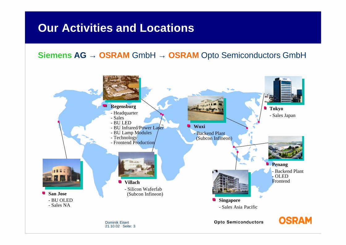
Dominik Eisert21.10.02 Seite: 3
Our Activities and Locations
San Jose- BU OLED- Sales NA
Tokyo- Sales Japan
Singapore- Sales Asia Pacific
Penang- Backend Plant- OLEDFrontend
Wuxi- Backend Plant (Subcon Infineon)
Regensburg- Headquarter- Sales- BU LED- BU Infrared/Power Laser- BU Lamp Modules- Technology- Frontend Production
Villach- Silicon Waferfab (Subcon Infineon)
Siemens AG → OSRAM GmbH → OSRAM Opto Semiconductors GmbH

Dominik Eisert21.10.02 Seite: 4
World Market by Product Segments
80801050
210880
95200
1180
275
990
115655
1320
340
1110
150
1060
1455
415
1240
195
1510
1610
485
1360
260
1825
1750
535
1480
305
2255
2000
650
1790
2300
3540
5850
51604320
2740
Source: OSRAM OS
Mill. Euro Mill. Euro VIS
VIS Aut
IR/HPL
OLED/ID
LM
99/00 00/01 01/02 02/03 03/04 04/05 05/06
19 %
13 %
31 %
12 %
150 %
19 %
29 %
12 %
24 %
12 %
228 %
21 %
22 %
12 %
22 %
10 %
62 %
30 %
19 %
10 %
17 %
11 %
42 %
30 %
13 %
9 %
10 %
9 %
21 %
33 %
c.a.g.r. 20 %20 %
21 %
21 %
14 %
24 %
17 %
13 %
21 %
11 %
74 %
25%
7000

Dominik Eisert21.10.02 Seite: 5
Material Systems for High Brightness LEDs
lattice parameter [Å]
band
gap
ener
gy [
eV]
wav
elen
gth
[nm
]
700600
500
400
AlN
1,0
1,5
2,0
2,5
3,0
3,5
4,0
2,5 3,0 3,5 4,0 4,5 5,0 5,5 6,0 6,5
6,2
InGaAlP
InN
SiC
GaN
InPGaAs
GaP
AlP
InGaN
Dominik Eisert21.10.02 Seite: 6
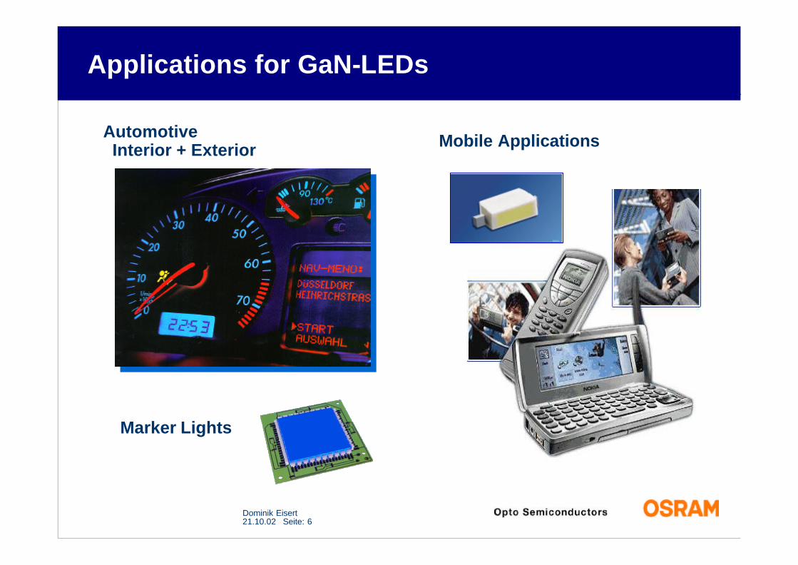
Applications for GaN-LEDs
Mobile ApplicationsAutomotive Interior + Exterior
Marker Lights

Dominik Eisert21.10.02 Seite: 7
Applications for LED Modules
Signal Lights
Illuminated Signs
Full Color Displays

Dominik Eisert21.10.02 Seite: 8
Are Semiconductors the Light of the Future?
0
50
100
150
200
1970 1980 1990 2000 2010 2020
Ligh
t Sou
rce
Eff
icie
ncy
[lm/W
]102
103
104
105
1970 1980 1990 2000 2010 2020
Ene
rgy
Con
sum
ptio
n [T
Wh]
Electricity
1.2 x10⁴ TWh
6.9 x10⁴ TWh
Energy
Illumination2.3 x103 TWh
USA: 20% of electr.BRD: 8% of electr.
World Energy Consumption p.a.
Incandescent
Halogen
Fluorescent
Semi-conductor
projected
Source: R. Haitz, Hewlett-PackardSource: International Energy Agency
Efficiencies of Light Sources
with acceler.effort
projected1998

Dominik Eisert21.10.02 Seite: 9
“White LED”
620
600
580
560
540
520
500
490
480
460
510
E
InGaN-chip generates blue light
partial conversionby a phosphore
color mixing⇒ WHITE
package
chipconverter

Dominik Eisert21.10.02 Seite: 10
Lamp Modules Applications:General Lighting
LED Modules for general lighting• information and orientation lighting
• effect lighting
• ambient lighting
LED Modules offerscreative design possibilities
extremely low-profile light solutions
high light output ratio
reduced maintenance costs

Dominik Eisert21.10.02 Seite: 11
Processes
Properties To Optimize
Parameters
Complexity of LED Production
Epitaxy
internal QE / gainmode control (LD)
voltage controldefects
growth kineticsMOVPE Reactor
Chip Processing
semiconductor processes
external QE (LED)mode control (LD)
voltage controlthermal management
Packaging
light extractionluminance
thermal managementmechanical properties
reliability
molding/castingmass production
Module
light distributionimagingcontrast
power drivers
systemintegration
heterostructure design
chip geometrycontacts
housing geometrypolymer materials
light guidesboard design

Dominik Eisert21.10.02 Seite: 12
LED Development Scenario
ProductIdea
Moore‘sLaw
Competition
DesignConcept
DesignVerification
CustomerProductReliability
ProcessDevelopment
Optimization?
TIME+COST
EpitaxyChip
i++
Concept Proof Process PackageLogistics
Simulation Simulation
Qua
litity
Mar
ketin
g
Sem
icon
duct
orD
evel
opm
ent
Pac
kage
Dev
el.
SimulationInformation

Dominik Eisert21.10.02 Seite: 13
0
1
2
3
4
5
6
Feb99
Mar99
Apr99
May99
Jun99
Jul99
Aug99
Sep99
Oct99
Nov99
Dec99
Jan00
po
wer
ou
tpu
t @
20m
A (
mW
)
0%
1%
2%
3%
4%
5%
6%
7%
8%
9%
10%
wal
lplu
g e
ffic
ien
cy
Brightness Development of InGaN QW-LED
Sapphire technology used by competitors
70µm
250µm
SiC-technologyfavored by Osram
deve
lopm
ent
of ep
itaxy
for 460nm blue LEDin 5mm Radial housing

Dominik Eisert21.10.02 Seite: 14
„Dark“ Transparent Substrate?
GaP-based chip GaN on SiC
Though 6H-SiC is transparent for blue light: no emission from substrate observed!
GaP SiC
GaN
angulardistribution

Dominik Eisert21.10.02 Seite: 15
Light Extraction from GaN/SiC-System
Transparent Substrate SiC (Eg=3.03eV) but n(GaN) < n(SiC)
Snell‘s law‚blind‘ angle (22°)
Light Extraction from SiC: θc=33°
n=1.5 n=2.7
θc
Incomplete Overlap ⇒ low efficiency
outcouplingangle (11°) ‚blind‘
angle
⇓GaN: n=2.5
SiC: n=2.7
Dominik Eisert21.10.02 Seite: 16
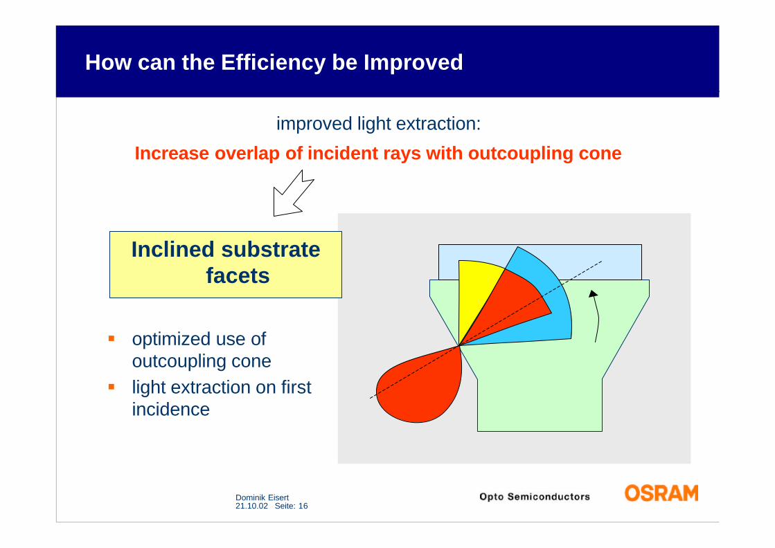
How can the Efficiency be Improved
improved light extraction:
Increase overlap of incident rays with outcoupling cone
Inclined substratefacets
§ optimized use ofoutcoupling cone
§ light extraction on firstincidence
Dominik Eisert21.10.02 Seite: 17
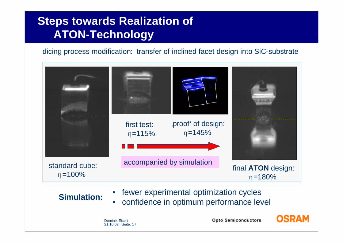
Steps towards Realization of ATON-Technology
standard cube: η=100%
first test: η=115%
‚proof‘ of design: η=145%
final ATON design: η=180%
dicing process modification: transfer of inclined facet design into SiC-substrate
• fewer experimental optimization cycles• confidence in optimum performance level
accompanied by simulation
Simulation:

Dominik Eisert21.10.02 Seite: 18
Raytracing Analysis
X
Objectivel of Chip Development: • optimize External Quantum Efficiency (EQE)
EQE hard to assess experimentally!
Non-sequential Raytracing Analysis ⇒ EQE + intensity distribution
+ complete geometrical 3D chip model + transparent + absorbing elements + scattering + interface to package development
− wave effects − electrical/thermal properties

Dominik Eisert21.10.02 Seite: 19
Optimization of Chip Shape
20
25
30
35
40
45
50
55
60
0 10 20 30 40 50 60 70 80 90Facet Angle (°)
Ext
ern
al Q
uan
tum
Eff
icie
ncy
(%
)
75µm100µm150µm
ATON footprint
Facet Angle
• optimum facet angle ≈30° ⇒ Doubling of Extraction Efficiency• limited by ohmic heating
ATON/socket ratio (290x290µm chip)
0
10
20
30
40
50
60
70
0 50 100 150 200
ATON footprint (µm)E
xter
nal
Qu
antu
m E
ffic
ien
cy (
%)
optical extraction efficiency
heating considered
ohmic heatgeneration
Dominik Eisert21.10.02 Seite: 20
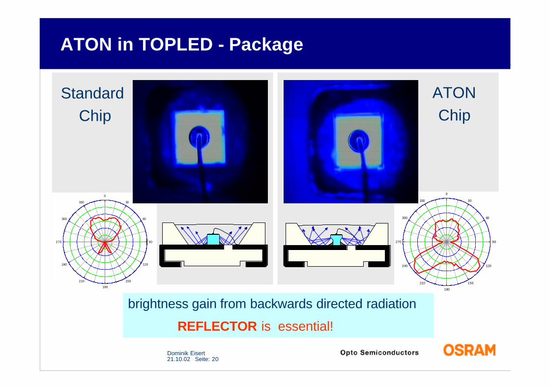
ATON in TOPLED - Package
Standard Chip
ATONChip
brightness gain from backwards directed radiation
⇒ REFLECTOR is essential!
0
30
60
90
120
150
180
210
240
270
300
3300
30
60
90
120
150
180
210
240
270
300
330

Dominik Eisert21.10.02 Seite: 21
Reliability of ATON Chip in Package:Mechanical Stresses
thermoplast
metal
epoxyLED-Package:materials with largely differingthermal expansion coefficients⇒ Delamination?
FEA shows no increased delamination risks for pyramidal chip
Dominik Eisert21.10.02 Seite: 22
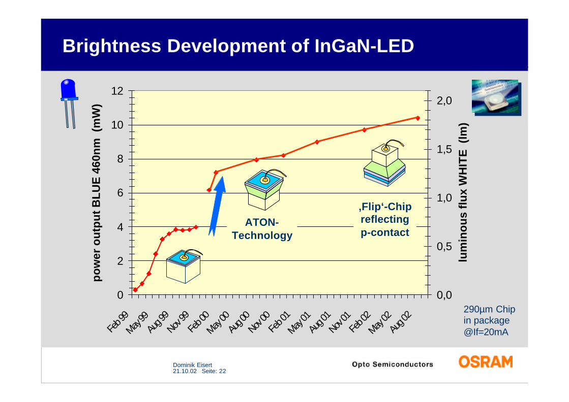
Brightness Development of InGaN-LED
0
2
4
6
8
10
12
Feb 9
9
May 99
Aug 9
9
Nov 99
Feb 0
0
May 00
Aug 0
0Nov
00Fe
b 01
May 01
Aug 0
1
Nov 01
Feb 0
2
May 02
Aug 0
2
po
wer
ou
tpu
t B
LU
E 4
60n
m (
mW
)
0,0
0,5
1,0
1,5
2,0
lum
ino
us
flu
x W
HIT
E (
lm)
ATON-Technology
‚Flip‘-Chipreflectingp-contact
290µm Chipin package@If=20mA
Dominik Eisert21.10.02 Seite: 23
0
10
20
30
40
50
60
200 400 600 800 1000
Chip Size (µm)
Ext
ern
al Q
uan
tum
Eff
icie
ncy
(%)
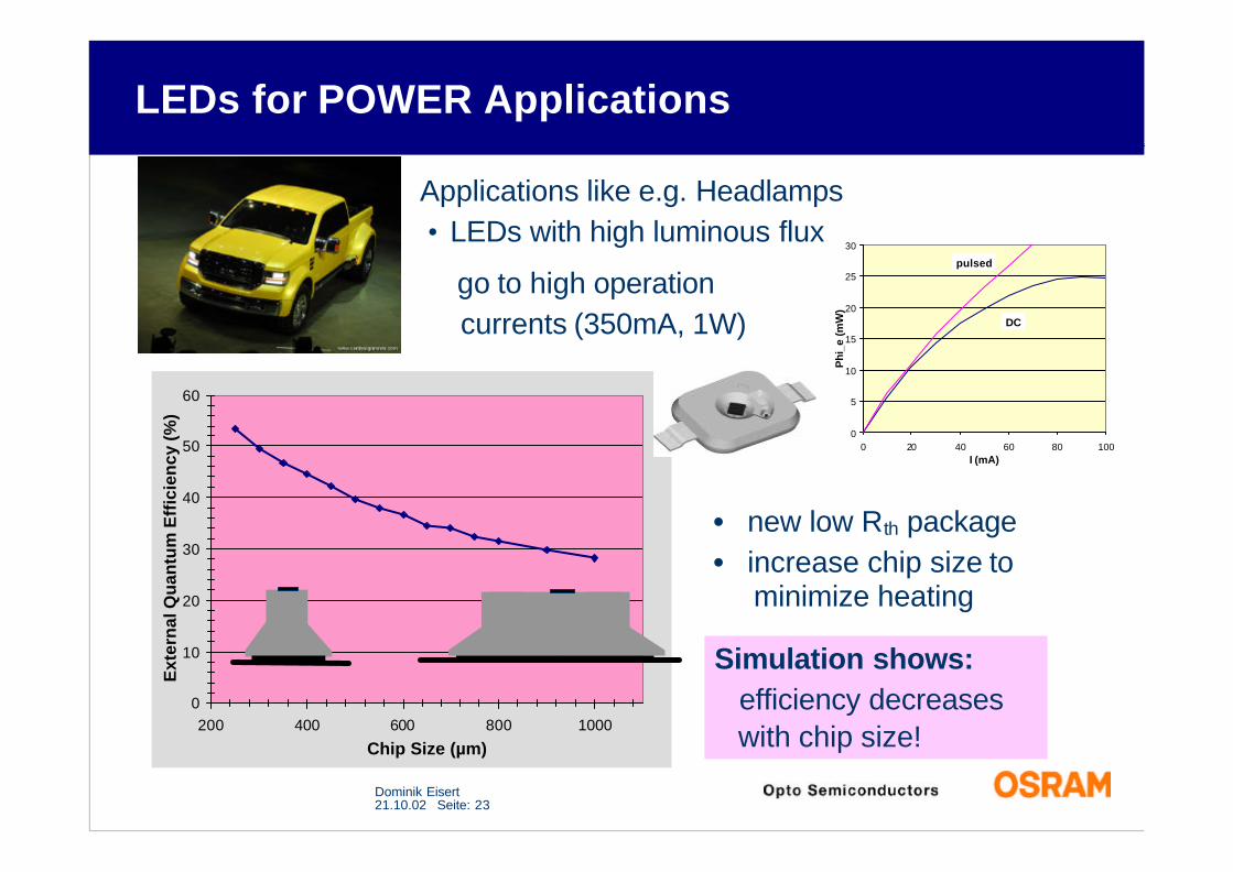
LEDs for POWER Applications
Applications like e.g. Headlamps • LEDs with high luminous flux
⇒ go to high operation currents (350mA, 1W)
• new low Rth package• increase chip size to minimize heating
Simulation shows: efficiency decreases with chip size!
0
5
10
15
20
25
30
0 20 40 60 80 100I (mA)
Phi
_e (
mW
)
DC
pulsed
Dominik Eisert21.10.02 Seite: 24
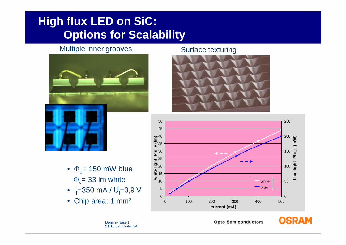
High flux LED on SiC: Options for Scalability
Multiple inner grooves Surface texturing
• Φe= 150 mW blue Φv= 33 lm white• If=350 mA / Uf=3,9 V• Chip area: 1 mm2
0
5
10
15
20
25
30
35
40
45
50
0 100 200 300 400 500current (mA)
wh
ite
ligh
t P
hi_
v (l
m)
0
50
100
150
200
250
blu
e lig
ht
Ph
i_e
(mW
)
whiteblue

Dominik Eisert21.10.02 Seite: 25
Potential Market Segments for Blue Laser Diodes
lighting
optical storage laser printing
medical technologyindustrial printing
technologyspectroscopy
...
projection - displays

Dominik Eisert21.10.02 Seite: 26
Structure of InGaN Laser Diode on SiC
SiC-substrate
buffer
GaN:Mg
GaN:Mg
GaN:Si
AlGaN:Mg
AlGaN:Si
GaInN/GaN MQW
Vertical Structure
p-dopedcladding
n-dopedcladding
wave guideactive zone
contact layer
SiC
InGaN SCH-Laser Diode• SiC substrate• vertical current flow• ridge wave guide• cleaved facets• dielectric mirror coating

Dominik Eisert21.10.02 Seite: 27
Work Packages with GaN Lasers on SiC
Indium fluctuations
Heterostructure design
CB
VBGaInN
Dislocations
lattice mismatch GaN/SiC 3.4%disloc. dens. up to 5x109cm2
epitaxial growth parameters
• number and depth of quantum wells• piezoelectric effect• wave guides
Reduction of Losses• p-contact• laser facets
• index guiding• laser mounting

Dominik Eisert21.10.02 Seite: 28
Minimize Threshold Current Density
• optimum number of quantum wells: 2-3
• electrical confinement vs. - piezoelectric effect - Indium phase separation
395 400 405 415 420 425 430
20
30
40
50
60
Indium content
thre
shol
d cu
rren
t den
sity
(kA
/cm
²)
emission wavelength (nm)
quantum well width: ~ 2 nm
390 410 435 1,0 1,5 2,0 2,5 3,0 3,5 4,0 4,530
35
40
45
50
55
thre
shol
d cu
rren
t den
sity
(kA
/cm
²)
quantum well width (nm)
gain guided, no mirror coatings
quantum well parameters
Dominik Eisert21.10.02 Seite: 29
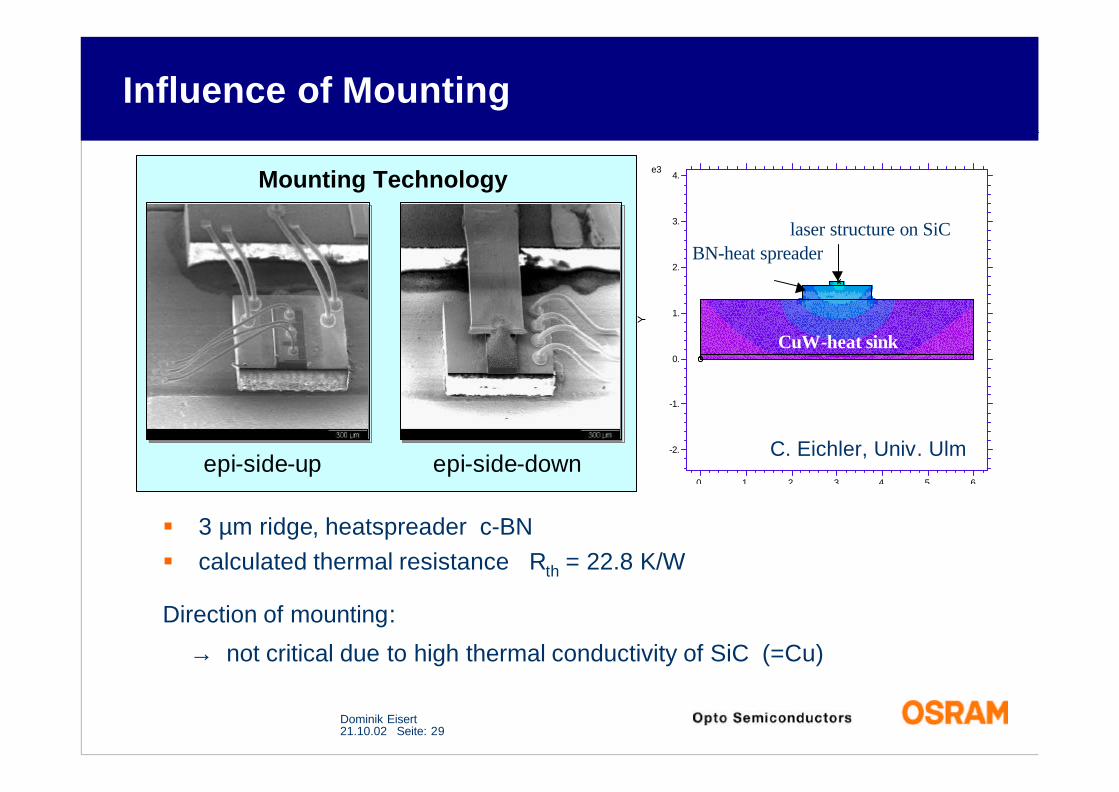
Influence of Mounting
§ 3 µm ridge, heatspreader c-BN§ calculated thermal resistance Rth = 22.8 K/W
Direction of mounting:
→ not critical due to high thermal conductivity of SiC (=Cu)
0. 1. 2. 3. 4. 5. 6.
Y
e3
-2.
-1.
0.
1.
2.
3.
4.
CuW-heat sink
BN-heat spreaderlaser structure on SiC
C. Eichler, Univ. Ulmepi-side-up epi-side-down
Mounting Technology
Dominik Eisert21.10.02 Seite: 30
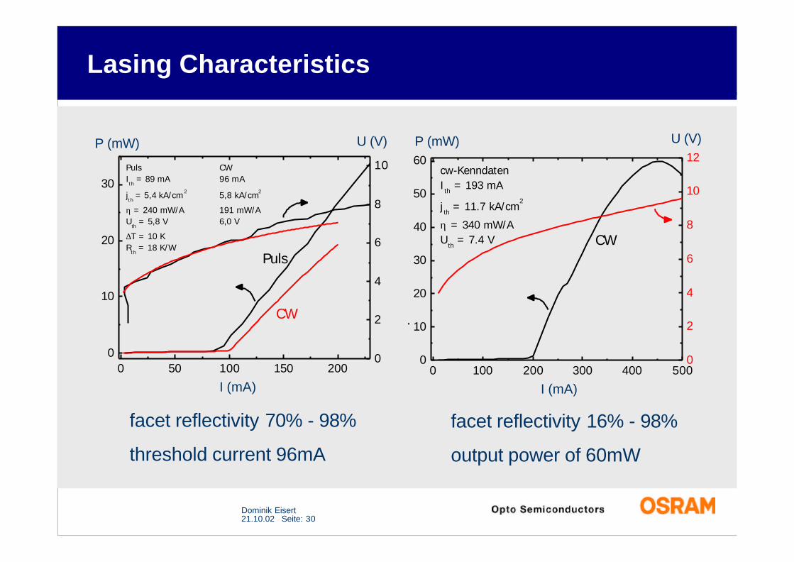
Lasing Characteristics
0 50 100 150 2000
10
20
30
0
2
4
6
8
10
CW
Puls
Puls- & cw-KennlinienPuls CWIth = 89 mA 96 mA
jth = 5,4 kA/cm2 5,8 kA/cm2
η = 240 mW/A 191 mW/AU
th = 5,8 V 6,0 V
∆T = 10 KR
th = 18 K/W
I (mA)
U (V)P (mW)
0 100 200 300 400 5000
10
20
30
40
50
60
0
2
4
6
8
10
12
CW
60 mW cw optische Leistung
opt.
Leis
tung
(m
W)
cw-KenndatenI
th = 193 mA
jth = 11.7 kA/cm
2
η = 340 mW/AU
th = 7.4 V
Spa
nnun
g (V
)
I (mA)
U (V)P (mW)
facet reflectivity 16% - 98%
output power of 60mW
facet reflectivity 70% - 98%
threshold current 96mA

Dominik Eisert21.10.02 Seite: 31
Lifetime Development
0,01
0,1
1
10
100
1000
Jul 01
Aug 0
1
Sep 0
1Okt 0
1
Nov 01
Dez 01
Jan 0
2
Feb 0
2Mrz
02Ap
r 02
Mai 02
Jun 0
2Ju
l 02
life
tim
e cw
@ 1
mW
[h
]
143h
ridge: 2.7x600µm
Rth: 18K/W
Ithr: 96mA
Uthr: 6V
Pel: 0.6W
Tpn: 35°C
Actual values
life time 143 h @ 1mW 54h @10mW
(first pulsed LD: 07/99 first cw LD: 03/01)
Dominik Eisert21.10.02 Seite: 32
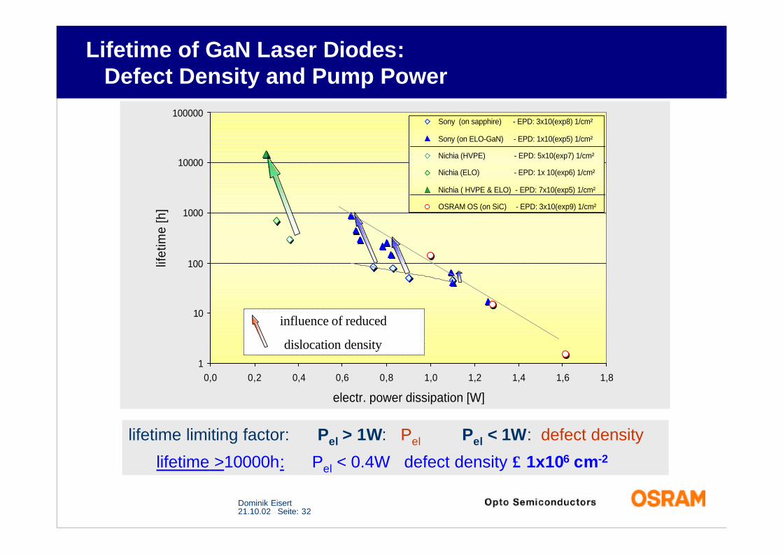
Lifetime of GaN Laser Diodes: Defect Density and Pump Power
1
10
100
1000
10000
100000
0,0 0,2 0,4 0,6 0,8 1,0 1,2 1,4 1,6 1,8
electr. power dissipation [W]
lifet
ime
[h]
Sony (on sapphire) - EPD: 3x10(exp8) 1/cm²
Sony (on ELO-GaN) - EPD: 1x10(exp5) 1/cm²
Nichia (HVPE) - EPD: 5x10(exp7) 1/cm²
Nichia (ELO) - EPD: 1x 10(exp6) 1/cm²
Nichia ( HVPE & ELO) - EPD: 7x10(exp5) 1/cm²
OSRAM OS (on SiC) - EPD: 3x10(exp9) 1/cm²
influence of reduced
dislocation density
lifetime limiting factor: Pel > 1W: Pel Pel < 1W: defect density
lifetime >10000h: Pel < 0.4W defect density ≤ 1x106 cm-2

Dominik Eisert21.10.02 Seite: 33
Simulations in the Development Processof GaN-based LEDs and Laser Diodes
ATON LED-Technology
Simulations inDevelopment
Benefit ofSimulations
InGaN LaserDiodes
Thanks
• 80% brightness improvement• makes SiC-technology highly competitive
• extensive use of Raytracing Simulations chip optimization, emission patterns, ...
• fast and linear progress• know-how basis for future projects
• life time of 143h optimizing GaN on SiC technology• next objective must be defect reduction
InGaN LED/LD devel. team, Process devel. groupPackage devel. group, External partners