simulation of traveling wave electro- absorption ...533304/fulltext01.pdf · simulation of...
TRANSCRIPT

Simulation of Traveling Wave Electro-absorption Modulators Suitable for
100Gbps
A k i n w u m i A b i m b o l a A m u s a n
Master of Science Thesis Stockholm, Sweden 2011
TRITA-ICT-EX-2011:144
MSc in Photonics
Erasmus Mundus MSc in Photonics
Erasmus Mundus
Simulation of Traveling Wave Electro-absorption Modulators Suitable
for 100Gbps
Akinwumi Abimbola AMUSAN
Promotor(s)/Supervisor(s): Associate Prof. Urban Westergren
Assisting supervisor(s): Associate Prof. Urban Westergren
Master dissertation submitted in order to obtain the academic degree of
Erasmus Mundus Master of Science in Photonics
Academic year 2010-2011
Simulation of Traveling Wave Electro-absorption Modulators
Suitable for 100Gbps
Akinwumi Abimbola AMUSAN
Master Thesis
Department of Photonics and Microwave Engineering (FMI) Royal Institute of Technology (KTH)
Stockholm, Sweden
June 2011

ii

iii
ABSTRACT
The large signal model for electro-absorption modulators is studied and simulated. In the
previous model, the effect of frequency chirp has not been included and also there is no phase
information of the optical carrier.
This thesis focuses on introducing the phase information of the optical carrier by representing it
as a time varying sinusoidal voltage as well as modeling frequency chirp in traveling wave
electro-absorption modulators by using a voltage dependent transmission line delay. The
transmission line is designed as periodic LC section, where all the capacitance values were
modeled to have a quadratic dependence on the microwave voltage using the CBREAK model in
PSPICE. This means that the transmission line delay will have a linear dependence on the
voltage.
The whole modified model for the modulator is then simulated and the frequency chirp effect on
the modulator performance was studied. It is shown that the frequency chirp broadens the
modulator spectrum but it has no pronounced effect on the eye diagram. This means that long
distance transmission will be mutilated due to dispersion.
By choosing a small absorption and large change in delay, the phase modulator is simulated and
can be fabricated by using a three step quantum well because it has a large change in refractive
index and small change in absorption. On the other hand, to fabricate an electro-absorption
modulator a rectangular quantum well should be used.
iv
ACKNOWLEDGMENT
My profound gratitude goes to my supervisor and promotor Urban Westergren who has been
helping me and giving me necessary support and ideas from the beginning of the thesis. Also
without the fund from the European Commission (Erasmus Mundus), the master program would
have been impossible for me and I will like to thank them for the funding.
Again my colleagues Glenn, Yassin and Mesut also gave their invaluable support with many
periods of discussion and rubbing minds as well as staying company with me at the electrum
while working. I will like to thank Chin Wan(Joanne) for helping me in proof reading.
Finally, I will also thank my dad, mum and siblings for their support and encouragement while
away from home.
v
TABLE OF CONTENTS
Abstract ......................................................................................................................................................iii
Acknowledgement .................................................................................................................................... iv
List of Figures .......................................................................................................................................... vii
List of Tables ............................................................................................................................................ ix
1. INTRODUCTION......................................................................................................................... 1
1.1 Motivation .............................................................................................................................. 1
1.2 Outline of the thesis ............................................................................................................... 2
2. BACKGROUND .......................................................................................................................... 3
2.1 Optical Modulators ................................................................................................................ 3
2.2 Basic Physics of Electro-absorption Modulators .............................................................. 5
2.3 Traveling Wave Electro-absorption Modulators (TWEAM) ........................................... 9
2.3.1 Ridge Waveguide Electro-absorption Modulator Structure .............................. 10
2.3.2 Relationship between Optical Absorption and Applied Voltage ..................... 12
2.3.3 Electrical Equivalent Circuit of TWEAM ........................................................... 13
2.3.4 Segmented Structures for Increasing Impedance of TWEAM ............................. 14
2.4 Statement of Problem .......................................................................................................... 15
3. MODELING FREQUENCY CHIRPING EFFECT IN TRAVELING WAVE
ELECTRO-ABSORPTION MODULATOR ......................................................................... 16
3.1 Effect of Frequency Chirping in Electro-absorption Modulators ................................. 17
3.2 Voltage Dependent Transmission Line delay Model for Frequency Chirping............. 19
3.3 Choosing the Voltage Variable Delay Line inductance and capacitance values ........ 20
3.4 Demodulation Section ......................................................................................................... 23
vi
3.5 Detecting the Frequency Change ....................................................................................... 23
4. SIMULATION RESULTS AND DISCUSSION .................................................................. 25
4.1 Influence of frequency chirp (change in delay factor) on the modulator
performance ................................................................................................................................ 25
4.2 Measuring the Change in Delay .......................................................................................... 28
4.3 Achieving an Electro-Optic / a Phase Modulator ............................................................ 32
4.4 Numerical Accuracies and Approximations ..................................................................... 33
5. SUMMARY AND CONCLUSION ......................................................................................... 35
Appendix
References

vii
LIST OF FIGURES
1.1 Cisco VNI Mobile 2011 [3] ............................................................................................................... 1
2.1 Franz-Keldysh Effect .......................................................................................................................... 6
2.2 Quantum well band gap in the absence of electric field ................................................................. 7
2.3 Quantum well band gap in the presence of electric field ............................................................... 7
2.4 Absorption Spectrum for Quantum Confined Stark Effect [10] ................................................... 8
2.5 Traveling-wave electro-absorption modulator [8] .......................................................................... 9
2.6 Vertical Cross Section of Typical Ridge Waveguide Structure for the modulator .................. 10
2.7 Confinement Factor against Mesa Width for two absorption layer thickness [11] .................. 11
2.8 Optical Absorption vs Applied Voltage [8] ................................................................................... 12
2.9 Equivalent circuit of incremental section of the modulator [8] .................................................. 13
2.10(a) Segmented traveling wave electro-absorption modulator [12] ........................................... 14
2.10(b) Fabricated I00 Gbps DFB-TWEAM integrated transmitter [4] .......................................... 14
3.1(a) Positive Chirp ................................................................................................................................ 18
3.1(b) Negative Chirp .............................................................................................................................. 18
3.2 Equivalent circuit of transmission line ........................................................................................... 19
3.3 Verifying the Capacitance Model with Low Pass Filter ............................................................... 20
3.4: Variable Delay Transmission Line ................................................................................................. 22
3.5 Block Diagram of the Modulator with 20 THz ac representing the light carrier frequency and
Modulating Voltage at 100 Gbps ........................................................................................................... 24
viii
4.1 Modulated waveform, Modulated Spectrum, and Eye Diagram with only fixed delay ........................ 25
4.2 Modulated waveform, Modulated Spectrum, and Eye Diagram with kdelay = 5 ................................ 26
4.3 Modulated waveform, Modulated Spectrum, and Eye Diagram with kdelay = 8 ............................... 27
4.4 Modulated waveform, Modulated Spectrum, and Eye Diagram with kdelay = 15 ............................. 27
4.5 Position of the carrier at the beginning of Modulator ‘ON’ state................................................ 28
4.6 Position of the carrier during the falling edge ................................................................................ 29
4.7 Position of the carrier at end of the falling edge ............................................................................ 29
4.8 Refractive Index Change at 2 V and 3 V drive voltage ................................................................ 31
4.9 Illustrating the change in delay by multiplying the reference and delayed signals .................. 32
4.10 Quantum Well With Large Absorption Change and Large Refractive Index Change .......... 33
4.11 Phase Modulation ............................................................................................................................ 33

ix
LIST OF TABLES
3.1 Capacitance value determined from versus Expected Capacitance determined from the
Capacitor Model Equation with R = 1 kΏ ........................................................................................... 20

1
CHAPTER ONE
INTRODUCTION
1.1 Motivation
The purpose of telecommunication is to convey information from the sender over a
communication channel to a receiver at some significant distance. Going from the historical
perspective, communication has always been part of human activities dated back to the antiquity
[1]. Different part of the world had their own form of communication for example using the
smoke signals and drums in Africa, America and certain part of Asia [2].
Over the years this field has seen rapid development from using smoke signals to using Morse
codes, telegraphy, telephones, then using coaxial cables and microwave signals. Again
transmission of electrical signal at high frequency suffer huge loss when using coaxial cables or
hollow metallic waveguides as the medium, this necessitate the use of another transmission
medium with low loss at high frequency. This problem was solved with the invention of lasers in
1960 as well as low loss fibers in 1970 [1] and this make fiber optic communication much more
possible.
Figure 1.1: Cisco VNI Mobile 2011 [3]

2
Moreover, fiber optic communication has been on rapid growth since its invention and the
capacity was increasing in multiple of thousands with the invention of low water peak fibers
having low loss, dispersion shifted and compensating fibers, erbium doped fiber amplifier over
the 1.55µm window and also Wavelength Division Multiplexing technology. Again the need for
this bandwidth kept increasing due to convergence between data, voice and video signal through
the internet, mobile data services, as well as face to face communication.
The growth in mobile data as predicted by Cisco in 2011 is as shown in figure 1.1. It is
anticipated that by 2015, the mobile video data will be bulk of all the data packets which will
increase the bandwidth further and the core network for the mobile service providers will need
more bandwidth.
Furthermore, the major components required for information encoding on optical carrier is the
modulators and this high bandwidth need could be provided by using the high speed travelling
wave electro-absorption modulators. Already effort has been made to increase the speed of this
device to 110Gbps in the concluded High-speed electro-optical components for integrated
transmitter and receiver in optical communication project in 2009 [4]. However it is necessary to
further optimize this device so as to again increase its speed and or provide more functionality
such as exploring the electro-optic effect in this device and reducing the parasitic chirp which are
of interest in this thesis.
1.2 Outline of the thesis
The first chapter gives some motivation for the subject, while the second chapter discusses some
necessary background in the subject. The third chapter focuses on modeling the frequency chirp
with a transmission line variable delay line and the fourth chapter highlights and discusses the
result obtained. Finally the fifth chapter gives the summary and conclusion.

3
CHAPTER TWO
BACKGROUND
2.1 Optical Modulators
Optical modulators are essential components required for fiber optics communication which are
used to imprint the information to be transmitted on an optical carrier. This is done usually in
two ways.
a) Direct Modulation
b) External Modulation
Direct Modulation
This is done by injection of current into the active region of semiconductor laser which in turn
controls the laser output. This is as a result of charge carrier control by current injection. A
semiconductor diode needs a threshold current where minimum population inversion is achieved
for lasing. Therefore, if a dc threshold bias is applied and a modulating ac signal is also applied
around this dc bias, then the output of the laser will vary proportionally with the modulating ac
voltage. Usually the most common modulation scheme is the on-off keying (OOK), which means
optical high intensity represents a binary one while low intensity represents binary zero.
The maximum bandwidth for directly modulated VCSEL recorded is 40GHz [5] and the
limitation is as a result of intra-band gain saturation at high optical power [6]. However, directly
modulated laser also suffer large frequency chirping, which is the change in its frequency during
transitions from zero to one, and this will greatly impair the transmission distance due to
dispersion.

4
External Modulation
In this scheme, the output of a continuous wave laser is fed into an external device which will
perform the modulation. External modulators are devices which are either based on electric field
controlled absorption or electric field controlled phase, which could later be turned into an
intensity modulation. The information signal is coded within the electric field which controls the
modulator output. Usually this type of modulators have better performance than the direct
modulator type because the external type has low parasitic chirp, which means longer
transmission distance could be achieved. Therefore, we can as well categorize external
modulators into two, namely:
Electro-optic Modulators
Electro-absorption Modulators
Electro-optic Modulators
The electro-optic modulator is based on refractive index (phase) change in the presence of
applied electric field (modulating signal), which can be converted to intensity modulation by
using a mach-zehnder interferometer design. The refractive index change can be due to Pockel’s
effect, which is a property obtained in non - centro symmetric crystals, where the refractive
index changes linearly with the applied electric field. Example of such crystal is Lithium
Niobate. Moreover, electro-optic effect has also been observed in silicon and some organic
polymers. Electro-optic modulator in silicon is due to free carrier dispersion effect which is as a
result of charge carrier modulation which affects both the real and imaginary part of the
refractive index [7].
Electro-absorption Modulators
This involves change in the optical extinction coefficient caused by applied electric field. This
usually occurs in semiconductor bulk materials and quantum wells. Generally they can be used
for intensity modulation, in which the presence of electric field correspond to high optical

5
absorption (OFF) and the absence of electric field correspond to low optical absorption (ON), as
shown below.
Drive V Optical Power
≡
Time Time
The basic physics for this change in absorption are Franz-Keldysh Effect in bulk semiconductors
and Quantum Confined Stark Effect in quantum well structures. These phenomenons will be
discussed in more details in the next section.
2.2 Basic Physics of Electro-absorption Modulators
The electro-absorption modulators are usually a p-i-n structure similar to a photo-detector but
with the difference that there is absorption of photons with energies below the bandgap of the
material for electro-absorption modulators, which is induced by the applied electric field. The
intrinsic layer is normally the absorption layer, and could either be a bulk material or a quantum
well. There are two basic mechanisms responsible for this absorption depending on the
absorption layer material type, these are namely:
a) Franz-Keldysh Effect (FKE)
b) Quantum Confined Stark Effect (QCSE)

6
Franz-Keldysh Effect (FKE)
This is the mechanism responsible for electro-absorption in bulk materials, which occurs due to
band to band excitation of electron from valence band to conduction band for photon energies
below the band gap. In other words, the electron hole pair in a depleted intrinsic region is excited
by impinging photon energy less than the band gap on it. This is as depicted below.
Electric Field
P Eo=hυo
i
E1=hυ1 n
Figure 2.1: Franz-Keldysh Effect
As shown in the figure above E1 < Eo, which means that the electric field causes the net band
gap to reduce and hence, absorption at that photon energy. We can also reason that the electron is
excited to a virtual state in the forbidden gap by the incident photon and then, tunnels into the
conduction band with the applied electric field. Usually the absorption materials used are III – V
semiconductor materials such as InGaAsP.
Quantum Confined Stark Effect (QCSE)
This occurs when a quantum well is used as the absorption material. This usually has a better
absorption performance because of the enhancement by exciton absorption peak present at room
temperature. A quantum well is a thin layer of lower band gap (well) material placed in between
two layers of higher band gap material (barrier), which means there is a band gap discontinuity at
the valence and conduction band which creates a potential well in both bands [9]. This is
illustrated below.

7
Ec Ee
ΔEc
Eg1 Eg2
ΔEv
Ev Ehh
Figure 2.2: Quantum well band gap in the absence of electric field
E-field
Figure 2.3: Quantum well band gap in the presence of electric field
Moreover, a quantum well allows strong interaction of electron and hole wave functions forming
an exciton. In the presence of electric field, the potential well appears tilted and there is an
exciton absorption for photon energy less than the difference between electron energy (Ee) in the
conduction band well and heavy holes energy (Ehh) in the valence band well. Consequently the
absorption spectrum shift to a higher wavelength (red shift) but the peak absorption reduces
because both wave functions moves towards opposite ends of the well and hence, reduction in
the overlap.

8
Figure 2.4: Absorption Spectrum for Quantum Confined Stark Effect [10]
In general, QCSE based modulators has the advantage of having higher change in absorption
with the electric field (modulation efficiency) and lower drive voltage but is also more
polarization and wavelength sensitive than the FKE based modulators. Besides, quantum well
structures also confine the charge carriers and some materials have a much heavy holes (e.g
unstrained InGaAsP / InGaAsP [8]), which is difficult to sweep away and hence, saturate at
lower power. Novel designs in the quantum well structures have been able to overcome some of
these disadvantages. For instance using InGaAs / InAlAs has a larger band gap offset for
electrons than holes, and also introducing some strain in the quantum well design [8].

9
2.3 Traveling Wave Electro-absorption Modulators (TWEAM)
Figure 2.5: Traveling-wave electro-absorption modulator [8]
Traveling wave structure means the optical field and the microwave field co-propagates.
Therefore, there will be non-linear interaction between the two fields. The modulator is no longer
traveling–wave if it is not terminated with an absorbing resistor. This means if there is no
matching, the microwave signal will just be bouncing back and forth, and the reflected
microwave field will no longer co-propagate (in same direction) with the optical field in that
situation.
Practical light intensity modulators are designed to satisfy quite a number of criteria. Since it will
always be connected to the drive electronics, then they must have a low drive voltage. This is
because electronics speed and breakdown voltage is limited by the Johnson’s limit, where the
product of both speed and breakdown voltage is a constant. Therefore, fast modulators must have
a low voltage. Apart from this, high speed modulators should also have impedance close to 50
ohms which is standard for high speed electronics, so as to match with the electronics and
prevent signal reflection. Again they should also have efficient electrical to optical conversion
around 1550nm optical window. In order words, the extinction ratio should be high enough,
typically 10dB for Ethernet application. The other criteria are low return loss, low chirp

10
characteristics, low polarization sensitivity, small size, monolithic integration with other devices
and low wavelength sensitivity.
The initial design was a lumped electrode type but such devices have a lower speed due to
capacitance of the lumped structure which causes a RC time constant limitation. This limitation
was overcame using the traveling wave electrode where a micro strip transmission line electrode
is used allowing both the microwave and optical signal to propagate and also properly match
with a terminating resistor. However it turns out that this distributed TWEAM structure has
lower impedance around 25ohms and hence, result in reflection. To solve the low impedance
problem, segmented structures have been developed with periodic high and low impedance
section so that the average impedance is close to 50 ohms [12].
2.3.1 Ridge Waveguide Electro-absorption Modulator Structure
BCB BCB
Figure 2.6: Vertical Cross Section of Typical Ridge Waveguide Structure for the modulator
(not drawn to scale)
Substrate N – InP
N – InP
Quantum Well Layer
AC GND
AC GND Intrinsic InP
P – InP
ELECTRODE

11
Figure 2.6 shows the vertical cross section of ridge waveguide structure for the modulators.
Starting with an n – type substrate, a n – type buffer layer will be grown on top of it, then later a
thin layer of the quantum well is grown on top of the buffer layer. The intrinsic layer is also
deposited on the quantum well to reduce the net capacitance. An upper cladding of n-InP is
doped with zinc so as to make it p-type and also grown on top of the intrinsic region. This is
followed by selective wet etching up to the top of the quantum well forming a ridge structure.
Ground metal planes are formed on the sides of the structure followed by metal planes on the
back side of the substrate for a dc bias. BCB (benzo-cyclobutene based polymer) is used to form
a planar structure and also to insulate the top electrode from the ground plane.
There is always a compromise between the capacitance and electric field across the quantum
well. A very thick intrinsic region will give a small capacitance (high impedance) but will also
reduce the electric field across the quantum well structure thus poor electro-optic efficiency. On
the other hand, thin intrinsic region will increase the electric field across the quantum well
structure and give good modulation efficiency but will also increase the capacitance (low
impedance) and hence causes reflection.
Figure 2.7: Confinement Factor against Mesa Width for two absorption layer thickness [11]

12
Apart from this, as shown in the figure above, choosing a narrow waveguide structure will give
high impedance but a low optical confinement and modulation efficiency. At the same time
choosing a thin absorption region will give higher modulation efficiency due to high overlap
between optical and microwave field, but gives a low impedance and hence also result in
reflection. In general, the position of the quantum well is chosen to have maximum overlap with
the electric field and also the device dimensions are optimized.
2.3.2 Relationship between Optical Absorption and Applied Voltage
The extinction ratio model for the electro-absorption modulator is as shown below.
Figure 2.8: Optical Absorption vs Applied Voltage [8]
From the previous work in [8], it has been shown that
(2.1)
Where p is constant, is the low field bias, E is the applied electric field, V is the driving
voltage, is the thickness of the absorption region, and c is the curvature parameter for device
optimization. In the fabricated device in [8], the optimum curvature parameter was determined to
be 1.8, and we can observe that the linear part of the curve is extended with a low bias voltage.

13
From the above expression, the extinction ratio is proportional to the applied voltage, but the
modulator driving voltage should be as low as possible. Furthermore, the relationship between
the optical absorption and the applied voltage is generally non linear, and this could help in
decreasing the bias and increasing the extinction ratio.
2.3.3 Electrical Equivalent Circuit of TWEAM
The equivalent circuit of the traveling wave electro-absorption modulator is used to determine
the microwave properties of the device. Basically, each part of the device is represented with an
equivalent electrical component in which the whole model can then be analyzed either by hand
analysis or much easier, by using simulation software such as PSPICE. This can go a long way in
optimizing the design of the modulator and obtaining much higher speed. The equivalent
electrical model for an incremental length of TWEAM is shown below.
L
Rc
Cint
Cext
Rp
I photo
Figure 2.9: Equivalent circuit of incremental section of the modulator [8]
Where L is the inductance of the transmission line electrode, Rc is the skin resistance of the
transmission line electrode, Rp is the resistance due to the active region which is mainly the p
section resistance, Cint is the internal capacitance of the active section, Cext is the capacitance
due to the fringe electric field and Iphoto is the photogenerated current.

14
2.3.4 Segmented Structures for Increasing Impedance of TWEAM
As earlier said, the transmission line structure was able to increase the bandwidth but at the
expense of low characteristic impedance which limits the speed due to reflection. Segmenting the
device into periodic sections of high and low impedance values will increase the modulator
impedance to near 50 ohms, while at the same time raise the speed of the modulator [12].
The schematic diagram of the fabricated device in KTH is as shown below.
(a)
(b)
Figure 2.10: (a) Segmented traveling wave electro-absorption modulator [12]
(b) Fabricated I00Gbps DFB-TWEAM integrated transmitter [4]

15
As shown in the figure, the absorption layer is made up of 8 - strained InGaAsP/InGaAsP
multiple quantum wells with n-type substrate and also n-InP cladding doped with zinc. The
active region is broken down into 4 sections with the first and third not having the transmission
line but the second and fourth having a transmission line electrode on top of it. We also have a
termination NiCr resistor used for matching.
2.4 Statement of problem
First this thesis is based on simulating the equivalent circuit for traveling wave electro-
absorption modulator with PSPICE, which will emphasizes on studying the optical propagation
by modeling the microwave characteristics. Previous works have been able to show the influence
of device geometrical dimensions on the modulator performance and optimization, developed a
better waveguide design and also showed the influence of large signal effect on the modulator.
This work will aim towards the following:
1. Instead of using a constant dc source as the optical carrier as in the previous work, we
will simulate a time varying ac signal (as the optical carrier) and see the effect on the eye
diagram.
2. Developing a more robust equivalent model which will take into account the frequency
chirping behavior (electro optic effect) of the modulator.
3. Show the influence of frequency chirp on the modulator with the model.
4. Show the possibility of achieving phase modulator, if the electro optic effect is dominant
(negligible electro-absorption).

16
CHAPTER THREE
MODELING FREQUENCY CHIRPING EFFECT IN TRAVELING
WAVE ELECTRO-ABSORPTION MODULATOR
The effect of applied electric field (modulating voltage) in traveling wave electro-absorption
modulators do not only induce optical absorption but also introduces some frequency variation
during logic transitions. This can be explained from the fact that the real and imaginary parts of
the refractive index of a material are coupled through Kramers-Kronig relation. We can
explicitly write their dependence as [13]:
(3.1)
Where PV is the principal value of Cauchy integral
This means that every time there is an absorption change, there will also be phase change
(refractive index change), and this phase change will reflect itself in the change in frequency,
since frequency change is the time derivative of phase. The change of the optical carrier
frequency with time is called frequency chirping and it usually occurs as the modulating voltage
switches.
We can further simplify Equation 3.1, for small signal modulation at the operating wavelength
to [13]:
(3.2)
Where, is the material chirp factor
A measurement model of absorption as a function of applied voltage was developed in [8] as:
(3.3)
Substituting equation 3.3 in 3.2 we have
17
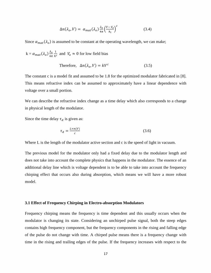
(3.4)
Since is assumed to be constant at the operating wavelength, we can make;
k =
and for low field bias
Therefore, (3.5)
The constant c is a model fit and assumed to be 1.8 for the optimized modulator fabricated in [8].
This means refractive index can be assumed to approximately have a linear dependence with
voltage over a small portion.
We can describe the refractive index change as a time delay which also corresponds to a change
in physical length of the modulator.
Since the time delay is given as:
(3.6)
Where L is the length of the modulator active section and c is the speed of light in vacuum.
The previous model for the modulator only had a fixed delay due to the modulator length and
does not take into account the complete physics that happens in the modulator. The essence of an
additional delay line which is voltage dependent is to be able to take into account the frequency
chirping effect that occurs also during absorption, which means we will have a more robust
model.
3.1 Effect of Frequency Chirping in Electro-absorption Modulators
Frequency chirping means the frequency is time dependent and this usually occurs when the
modulator is changing its state. Considering an unchirped pulse signal, both the steep edges
contains high frequency component, but the frequency components in the rising and falling edge
of the pulse do not change with time. A chirped pulse means there is a frequency change with
time in the rising and trailing edges of the pulse. If the frequency increases with respect to the
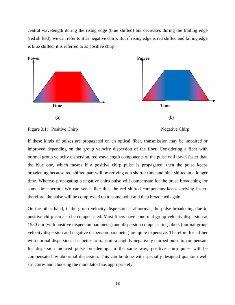
18
central wavelength during the rising edge (blue shifted) but decreases during the trailing edge
(red shifted), we can refer to it as negative chirp. But if rising edge is red shifted and falling edge
is blue shifted, it is referred to as positive chirp.
Power Power
Time Time
(a) (b)
Figure 3.1: Positive Chirp Negative Chirp
If these kinds of pulses are propagated on an optical fiber, transmission may be impaired or
improved depending on the group velocity dispersion of the fiber. Considering a fiber with
normal group velocity dispersion, red wavelength components of the pulse will travel faster than
the blue one, which means if a positive chirp pulse is propagated, then the pulse keeps
broadening because red shifted part will be arriving at a shorter time and blue shifted at a longer
time. Whereas propagating a negative chirp pulse will compensate for the pulse broadening for
some time period. We can see it like this, the red shifted components keeps arriving faster;
therefore, the pulse will be compressed up to some point and then broadened again.
On the other hand, if the group velocity dispersion is abnormal, the pulse broadening due to
positive chirp can also be compensated. Most fibers have abnormal group velocity dispersion at
1550 nm (with positive dispersion parameter) and dispersion compensating fibers (normal group
velocity dispersion and negative dispersion parameter) are quite expensive. Therefore for a fiber
with normal dispersion, it is better to transmit a slightly negatively chirped pulse to compensate
for dispersion induced pulse broadening. In the same way, positive chirp pulse will be
compensated by abnormal dispersion. This can be done with specially designed quantum well
structures and choosing the modulator bias appropriately.

19
3.2 Voltage Dependent Transmission line delay Model for Frequency Chirping
The optical propagation will be modeled as a voltage waves traveling on a transmission line. A
transmission line can be approximated with an infinite LC circuit with characteristics impedance
Z, as shown below
L/2
C
L
C
L
C
L
C
L/2
Figure 3.2: Equivalent circuit of transmission line
Where L = inductance per unit length
C = capacitance per unit length
In this type of structure there exists propagation speed and characteristics impedance given as:
(3.7)
This means if the capacitance or the inductance is dependent on the voltage, the propagation
speed changes which in turns vary the delay. In addition to the variation in delay, the
characteristics impedance also will change but we can get over this with proper matching with a
large resistor (attenuator).
If there is a quadratic relation between capacitance and voltage, then there will be a linear
dependence in delay.
That is, if then ,
this implies that, (3.8a)
Also,
(3.8b)

20
The capacitor CBREAK model in PSPICE was used to achieve the voltage variable capacitance.
Its uses a non-linear capacitor model [14]
Where and are linear and quadratic voltage coefficient, and are linear and
quadratic temperature coefficient. Normally and are zero.
The parameters were = 0, = 1000, K = 0.001 and value is the capacitance at zero
voltage. Since, we can assume approximately that
Therefore (3.9)
3.3 Choosing the Voltage Variable Delay Line inductance and capacitance values
1. First, the voltage variable capacitor was verified by performing a small signal ac simulation
for a RC low pass filter.
C
RVdc
Vac
Figure 3.3: Verifying the Capacitance Model with Low Pass Filter
Then the 3dB bandwidth was measured from the output of the ac simulation, and the capacitance
value was calculated from:

21
We can then compare this capacitance value with the expected values determined from the
capacitance model equation. At the same time, if we change the dc bias voltage, the capacitance
value should change. This is as shown in the table below
Table 3.1: Capacitance value determined from versus Expected Capacitance determined
from the Capacitor Model Equation with R = 1kΏ
Vdc (V) Capacitance (fF) determined
from
Capacitance (fF) determined from the model
equation with VC1 = 0, VC2=1000, K = 0.001 value
= 1fF
1.0 1.000999667 1.001
1.2 1.440994342 1.441
1.4 1.961002256 1.961
1.6 2.560984506 2.561
1.8 3.240982815 3.241
2.0 4.000978986 4.001
Therefore we can be sure that the voltage variable capacitor model varies as expected
2. Since the reflection is highly frequency dependent, the optical carrier was modeled with a 20
THz sinusoidal voltage to lower the reflection. Moreover, it is also important to make sure that
the variable delay transmission line has a cut off frequency well beyond 20THz. This was done
by also determining the frequency response for the LC circuit in figure 3.1 through ac
simulation. This will enable us to get the order of magnitude for the capacitance and inductance
per unit length. Therefore the capacitance and inductance values were order of magnitude 10-15
.
3. Also, it is necessary to choose the exact values for L and C that will give a particular delay.
Each length of the active section is 0.105 mm, which is divided into five slices, which means
length of each slice is 0.021mm. Assumed refractive index was 3.2 at zero voltage and this
corresponds to a time delay of:

22
Repeating equation (3.8)
Where, .
is the total capacitance in the whole transmission line length and has a unit of farad
while is capacitance per unit length. But the variation in delay is only about few percent of
the total delay. Typically the variable time delay section is 0.1 of the total delay. Again the
value of the transmission line impedance is not of importance if it is properly matched, although
it does not match at all voltages, therefore the impedance was chosen to be 4 when V=0.
The discretization error and the resonance frequency for the transmission line section depend on
the number of LC section. In actual fact infinite number of LC section will give the ideal
transmission line but it is impossible to model that one because of computational resources,
therefore the number of LC section chosen was 101. This will push the resonance well beyond
20THz. Hence capacitance and inductance per unit length are:
The capacitance value will change with voltage and the delay.
4. The block diagram of the variable delay section is as shown below.
R
R_scVop+
Vop-
Vm+
Vm-
R
High Pass Filter
Out-
Out+ LC Section
Figure 3.4: Variable Delay Transmission Line

23
Vop is the time varying optical carrier while Vm is the applied microwave signal. The optical
carrier Vop is much lower than the microwave signal Vm. Hence, the delay is majorly controlled
by the microwave signal. Apart from this, a high attenuator resistor was placed before the
transmission line to reduce reflection. Finally, the high pass filter will remove the microwave
signal so that we will only have the optical carrier with some propagation delay at the output.
3.4 Demodulation Section
In the simulations, a 20 THz ac signal represents the optical carrier, modulated by 100 Gbps
PBRS signal. The resulting waveform is an amplitude modulated carrier. In order to retrieve the
modulating signal back, a simple demodulator circuit was used, which consist of a diode and a
low pass filter.
3.5 Detecting the Frequency Change
Until now, we have modeled the change in frequency of the optical carrier during the rise and
fall time of the modulating signal, which results into a parasitic frequency or phase modulation.
This can be observed if we superimpose the input reference signal on the delayed carrier signal,
which will result to a relative time shift between both signals (input and delayed signal) around
the zero amplitude voltage point. This time shift changes along the rise and fall edge of the
modulating voltage. This will be discussed in more detail in the next chapter and the modulator
block diagram is as shown in figure 3.5.
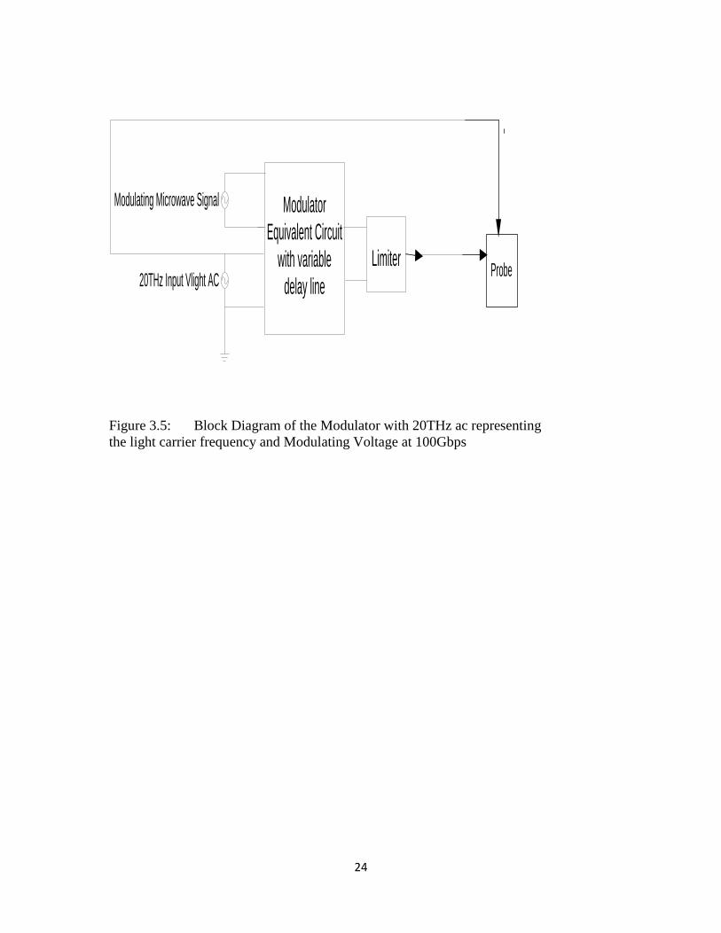
24
Modulator
Equivalent Circuit
with variable
delay line20THz Input Vlight AC
Modulating Microwave Signal
LimiterProbe
Figure 3.5: Block Diagram of the Modulator with 20THz ac representing
the light carrier frequency and Modulating Voltage at 100Gbps

25
CHAPTER FOUR
SIMULATION RESULTS AND DISCUSSION
This chapter presents the effect of the simulation parameters on the eye diagram, particularly on
the effect of increasing the voltage dependent change in delay (frequency chirp) on the
performance of the modulator and the measurement of the change in delay. The modulator model
used consists of two active segments and three passive segments, and the parameters were
chosen based on the previous designs in the department.
4. 1 Influence of frequency chirp (change in delay factor) on the modulator performance
First, assuming there is no change in delay (no frequency chirp) in the modulator, we expect a
perfect eye opening without distortion provided all other parameters are chosen rightly. For
instance in the simulation, we would have a good eye opening if the optical power is 1 mW
(though modeled as mV in PSPICE), the modulating voltage is 2 Vpp and the bias voltage is 0.2
V. The simulation result below shows the modulated signal, modulated signal spectrum and the
eye diagram in an ideal situation without frequency chirp.
Figure 4.1: Modulated waveform, Modulated Spectrum, and
Eye Diagram with only fixed delay
The spectral components show the carrier frequency
and side bands due to amplitude modulation.

26
While keeping other parameters constant, the delay is now increased in steps, we can observe the
tolerance of the modulator to frequency chirp with the eye diagram and spectra components of
the signal. Considering three extreme cases when the delay is increased by a factor if 5, 8 and 15,
the change in time delay can be determined from
Where V changes from 0 to 2V, Lt and Ct are the total transmission line inductances and
capacitances which were determined as 0.896fH and 0.056fF. There are two active segments,
with each segment divided to 5 portions and the corresponding total change in delay for the
factor kdelay = 5, 8 and 15 are 4.48fs, 7.2fs and 13.4fs respectively. If these changes in delay are
introduced, the resulting modulator performances are shown below.
Figure 4.2: Modulated waveform, Modulated Spectrum, and Eye Diagram with kdelay = 5

27
Figure 4.3: Modulated waveform, Modulated Spectrum, and Eye Diagram with kdelay = 8
Figure 4.4: Modulated waveform, Modulated Spectrum, and Eye Diagram with kdelay = 15
28
As seen from the figures, the performance of the eye diagram is relatively the same for the three
cases but with a slight increase in overshoot undershoot and time jittering as the delay is
increased. The eye width and height is also comparable to the cases when there is no voltage
dependent delay. This implies that some time shift of the carrier period may not cause a
significant change in the eye diagram. On the other hand the spectral components increases with
the delay and this will cause significant impairment for long distance transmission due to
dispersion. Although the immediate modulator eye diagram is not so distorted, the signal will
still be mutilated as the transmission distance is increased.
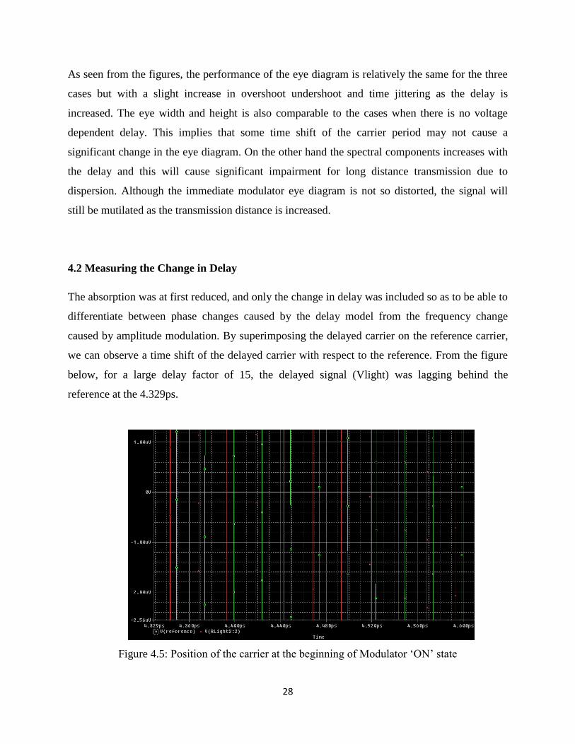
4.2 Measuring the Change in Delay
The absorption was at first reduced, and only the change in delay was included so as to be able to
differentiate between phase changes caused by the delay model from the frequency change
caused by amplitude modulation. By superimposing the delayed carrier on the reference carrier,
we can observe a time shift of the delayed carrier with respect to the reference. From the figure
below, for a large delay factor of 15, the delayed signal (Vlight) was lagging behind the
reference at the 4.329ps.
Figure 4.5: Position of the carrier at the beginning of Modulator ‘ON’ state

29
As the applied voltage tends to change state, that is the rising and falling edges, the optical
carrier shifts in time. Moreover, during the falling edge the time shift increases in the positive
direction as the modulator negative applied voltage is increasing. At some point the Vlight
becomes in phase with the reference signal and this is shown in figure 4.6. Again, as the delay
continues increasing, the optical carrier leads the reference signal at end of the falling edge in
figure 4.7.
Figure 4.6: Position of the carrier during the falling edge
Figure 4.7: Position of the carrier at end of the falling edge

30
The shift in time along the falling edge was measured from the probe for different delay factor.
This is as shown below.
Kdelay Measured Time Shift (fs)
2
4
6
8
10
V=2V V=3V
2.2
4.2
6.2
8.5
11.5
2.4
9.5
13
17.7
23.8
The time shift obtained above was when 20 THz was used as the optical carrier. The phase shift
corresponding to 200THz will be 10 times that of 20THz.
The refractive index change can be obtained from the shift in time from the relation:
Where the total length of the active segment was 210 μm and c is the speed of light. The
refractive index change at different factor increment and also modulating voltage is plotted in the
graph below
31
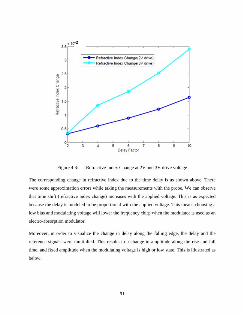
Figure 4.8: Refractive Index Change at 2V and 3V drive voltage
The corresponding change in refractive index due to the time delay is as shown above. There
were some approximation errors while taking the measurements with the probe. We can observe
that time shift (refractive index change) increases with the applied voltage. This is as expected
because the delay is modeled to be proportional with the applied voltage. This means choosing a
low bias and modulating voltage will lower the frequency chirp when the modulator is used as an
electro-absorption modulator.
Moreover, in order to visualize the change in delay along the falling edge, the delay and the
reference signals were multiplied. This results in a change in amplitude along the rise and fall
time, and fixed amplitude when the modulating voltage is high or low state. This is illustrated as
below.

32
Figure 4.9: Illustrating the change in delay by multiplying the reference and delayed signals
From figure 4.9, the red curve is a period of the modulating signal while the green curve is the
result of multiplication of reference and delayed signals. We can see that the amplitude only
changes during the fall time, which means that there is a change in time shift. And as earlier
shown, the delay in the carrier remains constant when the modulating voltage is zero. Moreover,
along the fall time of the modulating signal, this time shift increases. Then it remains constant at
a fixed value when the modulating voltage is negative -200nV. The reverse situation occurs
when the modulating voltage is rising.
4.3 Achieving an Electro-Optic / a Phase Modulator
With the model, it will be possible to design a phase modulator by choosing a large delay factor
and low absorption. It has been shown that the design of the quantum wells can inherently
change the property of the modulator and that a 3-step quantum well would give a large electro-
optic change [15]. This is illustrated below.

33
Figure 4.10: Quantum Well With Large Absorption Change and Large Refractive Index
Change [15]
We will have to choose between the two quantum well designs depending on the type of
modulator we are interested in. For an electro-absorption modulator, a rectangular quantum well
would be used because it gives a large change in absorption and small change in refractive index
while on the other hand, a three step quantum would be suitable for phase modulators because it
gives a large refractive index change and a small absorption change. Therefore if a specific
voltage is chosen and the desired change in delay, we can model a phase modulator. This can be
illustrated below.
²²
Figure 4.11: Phase Modulation

34
A global picture of the delay change with voltage along the voltage transition is shown above.
We can observe a change in phase and the carrier takes a different phase at voltage level zero and
one. Therefore, there is a modulation of the carrier phase by the microwave voltage.
4.4 Numerical Accuracies and Approximations
The optical carrier was modeled as a 20 THz voltage source because of the sensitivity of the
design to reflections which is large at higher frequencies. This does not correspond to the exact
frequency at 1.55 μm (193 THz) but could also give an idea of how the phase will change at 193
THz. The phase change at 200 THz carrier is simply 10 times the phase change at 20 THz
carrier.
Moreover, to have a very large change in delay, higher number of LC sections has to be used to
shift the resonance to higher frequency because this will influence the absorption characteristics
of the modulator if there is resonance in the transmission line transfer function. Moreover, there
are certain instances where the simulations do not converge. This was solved by taking a smaller
time step ceiling (calculation step) and also by increasing the absolute tolerance. However,
taking a large absolute tolerance will affect the resolution of the output. Therefore, one has to
determine the lowest tolerance that is just sufficient for the program to converge. Finally, the
linear dependence of the delay with voltage was approximated with the capacitor CBREAK
model in PSPICE by taking large value of the quadratic voltage coefficient.

35
CHAPTER FIVE
SUMMARY AND CONCLUSION
The phase information of the optical carrier has been included in the model by using a time
varying signal to represent the optical carrier and also introducing a voltage dependent time
delay to mimic frequency chirp. This has given a closer approximation to the complete physics
of the modulator. Moreover it was also found that the frequency chirp does not have significant
effect on the immediate modulator eye diagram but would increase the spectral components and
this will limit the modulator in long distance transmission due to dispersion.
Again, by reducing the absorption coefficient and increasing the delay (refractive index) change,
we can model a phase modulator. In reality this would be designed be selecting the type of
quantum wells that is rectangular quantum well for electro-absorption modulators and three step
quantum well for phase modulators.
The drawback of the design is that the exact optical frequency was not used. Only 20 THz was
used to model the optical carrier because of the design limitations such as increased reflections at
higher frequency. On the other hand the change in phase at 200 THz will be 10 times that of 20
THz. Also, the measurement of the change in delay was done manually with the output probe in
PSPICE. This can be further improved in future work.
Finally the numerical approximations would affect the resolution of the output and this may be
improved by reducing the absolute tolerance and the calculation time step. However, taking too
small tolerance values may give a convergence problem and in principle one would determine
the smallest relative tolerance that will make the simulation converge.
36
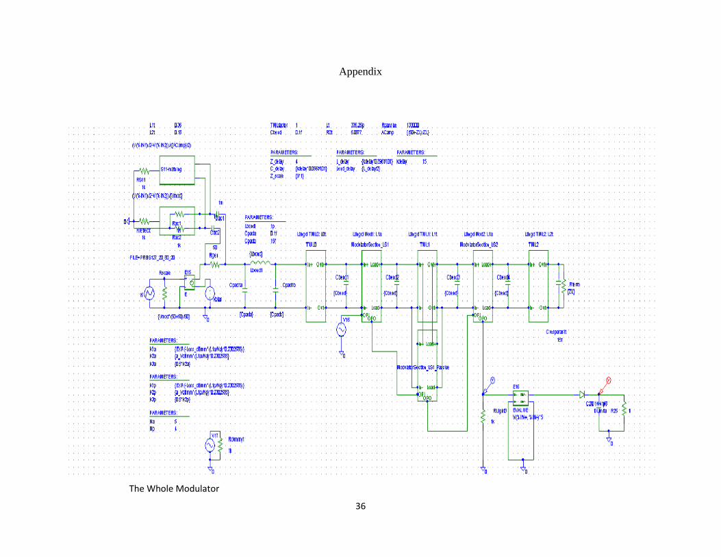
Appendix
The Whole Modulator

37
Modulator Active Segment

38
The beginning of the Variable Delay Transmission Line Section (101 LC Sections)

39
Modulator Passive Section

40
Parameters Settings
41
References
1. Govind P. Agrawal. Fiber-Optic Communication Systems. John Wiley & Sons, Inc., 3
edition, 2002.
2. http://en.wikipedia.org/wiki/History_of_telecommunication 9th
April 2011 at 20:43
3. White Paper, Cisco Visual Networking Index: Global Mobile Data Traffic Forecast
Update, 2010–2015
4. http://www.hecto.eu/.
5. Lucas Chrostowski, Behnam Faraji, Werner Hofmann, Markus-Christian Amann,
Sebastian Wieczorek, and Weng W Chow, 40GHz Bandwidth and 64GHz Resonance
Frequency in Injection-Locked 1.55μm VSCELs, IEEE Journal of Selected Topics in
Quantum Electronics, Vol 13, No 5 ,2007 September,
6. Electronic Letters June 1990, Vol. 26 No. 13
7. G. T. Reed, G. Mashanovich, F. Y. Gardes and D. J. Thomson, Silicon optical
modulators, Nature Photonics, Review Articles Focus, Vol 4,August 2010
8. Robert Lewén, High-Speed Electroabsorption Modulators and p-i-n Photodiodes for
Fiber-Optic Communications, Doctoral Dissertation, Royal Institute of Technology,
Department of Microelectronics and Information Technology, Stockholm 2003
9. William S. C. Chang, Fundamentals of Guided-Wave Optoelectronic Devices,
Cambridge University Press 2010
10. Gebirie Yizengaw Belay, Investigation of Large Signal Effects on Travelling Wave
Electro-absorption Modulator Performance and Optimization, Master dissertation,
Erasmus Mundus Master of Science in Photonics, Department of Photonics and
Microwave Engineering (FMI), Royal Institute of Technology (KTH), June 2010
11. Akinwumi Amusan, Modal Study of Optical Waveguide for Electro-absorption
Modulators, Individual Project Report, Simulation of Semiconductor Devices Course,
Royal Institute of Technology, 2010/2011.
12. Robert Lewén, Member, IEEE, Stefan Irmscher, Urban Westergren, Member, IEEE, Lars
Thylén, Member, IEEE, Member, OSA, and Urban Eriksson, Segmented Transmission-

42
Line Electroabsorption Modulators Journal of Light wave Technology, Vol. 22, No. 1,
January 2004
13. Ivan P. Kaminow, Tingye Li, Alan E. Willner, Optical Fibre Telecommunications, A:
Components and Subsystems, Elsevier, 2008
14. Microsim Corporation, The Design Centre: Circuit Analysis Reference Manual, January
1994
15. H. Mohseni, H. An, Z. A. Shellenbarger, M. H. Kwakernaak, and J. H. Abeles, Enhanced
Electro-Optic Effect in GaInAsP-InP Three- Step Quantum Wells, Applied Physics
Letters, Volume 84, Number 11, 2004