simulation of neutron radiation effects in silicon ... · the ems electromagnetic calorimeter, and...
TRANSCRIPT

Simulation of Neutron Radiation
Effects in Silicon Avalanche
Photodiodes
Thesis submitted for the degree of Doctor of Philosophy
by
Mark David Osborne
Faculty of Technology, BruneI University
November 2000

Abstract
A new one-dimensional device simulation package developed for the simulation
of neutron radiatiol! effects in silicon avalanche photodiodes is described. The soft
ware uses a finite difference technique to solve the time-independent semiconductor
equations across a user specified strllcture. Impact ionisation and illumination are
included, allowing accurate simulation with minimal assumptions about the device
under investigation. The effect of neutron radiation damage is incorporated via the
introduction of deep acceptor levels subject to Shockley-Read-Hall statistics.
Two models are presented. A reverse reach through model, based on the EG&G
C30626E reverse reach through avalanche photo diode originally proposed for use in
the eMS electromagnetic calorimeter, and a reach through model, based on widely
available commerical devices. A short experimental study on two commercial silicon
avalanche photodiodes, a C30719F reverse reach through APD and a C30916E reach
through APD, is presented for comparison with the simulation data. To allow full
comparis~n with the simulated predictions, the commercial devices were irradiated
at the Rutherford Appleton Laboratory's ISIS facility.
The simulated data shows good qualitative agreement with the measurements
performed on the commercial devices, quantitative predictions would require exact
information about the doping profile. The characteristic behaviour of the devices is
predicted over a wide range of conditions both before and after neutron irradiation.
The effect of ionised deep acceptors in the bulk of the devices is investigated. The
simulation package provides a useful tool for the analysis of semiconductor devices,
particularly in areas where a non-ionising radiation damage is prevelent e.g. high
energy physics, and provides a good basis for further development.

11
To my family

III
Acknowledgements
Firstly I would like to thank my supervisors, Peter Hobson and Steve Watts. I
appreciate all their efforts, from start to end, in helping to get this work completed
and especially the thesis written. Thanks also to PPARC for funding my Ph.D.
I would also like to thank all the other staff who have helped me along the way:
Derek, Andrew, Chris ,Barry and of course Sabah!
A special mention to the people who kept me sane at the most insane times: N 0-
tably Karl (who I will ring one day), Kate, Mita, Babara, Max, Dave, Jane, Mabu,
Rye, Paul and John.
Thankyou to all my family who have helped enormously, especially mum, dad,
gran and grandad. An endless thankyou to Clare and the boys for keeping me smil
ing all the way through.
This thesis is dedicated to the memory of Leonard Childs.

Contents
1 Overview 1
1.1 Introduction. .......... 1
1.1.1 Optical Photo-Detectors 1
1.1.2 The Photomultiplier Tube 2
1.2 PIN Photodiode . . . . 4
1.3 Avalanche Photodiode 6
1.3.1 High Energy Physics 8
1.4 The Compact Muon Solenoid Electromagnetic Calorimeter 8
1.4.1 Overview of CMS 8
1.4.2 The ECAL ... 9
1.4.3 Application of APDs 11
1.4.4 Introducing the Simulation. 12
1.5 Overview of Thesis ......... 13
2 APD Device Theory and Operation 15
2.1 Introduction .......... 15
2.2 The Semiconductor Equations 16
2.2.1 Introduction . . . . . . 16
2.2.2 The Current Equations . 17
2.2.3 The Continuity Equations 19
2.2.4 The Poisson Equation 19
2.3 The PN Junction .. 20
2.3.1 Introduction . 20
1

CONTENTS 11
2.3.2 Thermal Generation and Recombination Processes . 21
2.3.3 Indirect Recombination ................ 22
2.3.4 Additional Generation and Recombination Processes 26
2.3.5 Impact Ionisation 26
2.3.6 Excess Noise. . . 31
2.3.7 Ionisation Co-efficients 32
2.4 Photo-detection . . . . 32
2.4.1 Photoexcitation 32
2.5 Junction Photodiodes . 33
2.5.1 PIN Photodiodes 34
2.5.2 Avalanche Photodiodes . 34
2.5.3 Germanium Avalanche Photodiodes . 34
2.5.4 Hetero-J unction Avalanche Photodiodes 35
2.5.5 Reach Through Avalanche· Photodiodes . 36
2.5.6 Reverse Reach Through Avalanche Photodiodes 38
2.6 Fast Neutron Radiation Damage. 39
2.7 Macroscopic Effects in Silicon 40
2.8 Damage Mechanism. 41
2.9 Annealing ...... 44
3 Experimental Techniques 45
3.1 Introduction . . . 45
3.2 The Test System 45
3.2.1 Introduction . 45
3.2.2 Temperature Control 46
3.2.3 Bias Control . 48
3.2.4 Illumination . 49
3.3 Experimental Procedures. 53
3.3.1 Introduction . . . . 53
3.3.2 The Constant Illumination Gain. 53

CONTENTS 111
3.3.3 Photosensitivity . . . 55
3.3.4 Excess Noise Factor . O,J
3.3.5 Errors ..... 56
3.3.6 Post Irradiation 57
4 Simulation of Avalanche Photo diodes. 59
4.1 Introduction 60
4.2 APDSIM .. 61
4.2.1 Introduction. 61
4.2.2 Semiconductor Equations 63
4.2.3 The One-Dimensional Grid. 64
4.2.4 Grid Parameter Selection. 64
4.2.5 Discretisation Error. . . . 67
4.2.6 Application of Finite Differences. 67
4.2.7 Linearising the Discretised Equations 69
4.2.8 Solving the Matrix Equation ..... 70
4.2.9 Initialising and Terminating the process 72
4.2.10 Impact Ionisation 75
4.2.11 Illumination ... 78
4.2.12 Neutron Radiation Damage 80
4.3 APDGAIN ...... 82
4.3.1 Introduction. 82
4.3.2 Multiplication Factor. 83
4.3.3 Excess Noise Factor . 84
4.4 DIFFUSE . . .... 85
4.4.1 Introd uction . 85
4.5 Simulation Limitations 86
4.5.1 Introduction . 86
4.5.2 APDSIM .. 86
4.5.3 APDGAIN 87

CONTENTS
4.5.4 DIFFUSE 88
4.6 Conclusions 88
5 Results 89
5.1 Introd uction . 89
5.2 Pre~ Irradiation 91
5.2.1 Introd uction . 91
5.2.2 11icroscopic Features 92
5.2.3 Dark Current 99
5.2.4 Photocurrent · 100
5.2.5 Gain ..... · 101
5.2.6 Excess Noise Factor . · 105
5.2.7 Photosensitivity . · 109
5.3 Post-Irradiation ..... · 112
5.3.1 Reach Through APD · 112
5.3.2 Reverse Reach Through APD · 119
6 Conclusions 128
A 142
B 146
C 149

List of Tables
1.1 Table showing typical values of gain and response time for a variety
of semiconductor photo-detectors. . . . . . . . . . . . . . .
1.2 Table showing the properties of various scintillating media. 9
1.3 Table showing the desired and measured parameters of the candidate
APDs for the CMS ECAL . . . . . . . . . . . . . . . . . . . . . . .. 12
2.1 Table showing the parameters used in the Chenowyth expression for
the ionisation co-efficients. . . . . . . . . . . . . . . . . . . . . . . " 27
2.2 Table showing the stated typical characteristics of the C30916E and
C30719F APD at 22°C. . . . . . . . . . . . . . . . . . . . . . . . . . . 38
4.1 Table showing several types of semiconductor model .
4.2 Table showing the convergence time and steps for various grid sizes
61
66
4.3 Table showing the properties of the deep acceptor level used in the
simulation.. . . . . . . . . . . . . . . . . . . . . . . . . . . . . . . .. 81
5.1 Table showing the specifications of each of the diffused implants used
to create the reach through model. ................... 89
5.2 Table showing the specifications of each of the diffused implants used
to create the reverse reach through APD model. . . . . . . . . . . . . 90

List of Figures
1.1 A figure showing the visible region of the electromagnetic spectrum. 2
1.2 A schematic of a typical photomultiplier tube. . . . . . . . . . . .. 3
1.3 A simple diagram showing how the valence band electrons are excited
into the conduction band by an incident photon. . . . . 5
1.4 A simple schematic of a typical sHcon PIN photodiode. 6
1.5 A simple schematic of a typical silicon reach through avalanche pho-
todiode. . . . . . . . . . . . . . . . . . . . . . . . . . . . . . . . . .. 7
1.6 A figure showing the CMS detector due to start running at the Large
Hadron Collider at CERN in 2005. ................. .. 10
1.7 A simple schematic showing the electric field profiles and gain regions
of the EG&G reach through and reverse reach through APDs. . . .. 14
2.1 A simple diagram showing indirect recombination. . 21
2.2 A simple diagram showing direct recombination. . . 22
2.3 A diagram showing the processes involved in indirect recombination.. 23
2.4 A band diagram showing the process of impact ionisation. ...... 27
2.5 Figure showing the values of a e and ah calculated using the Chenowyth
parameterisation. . . . . . . . . . . . . . . . . . . . . . . . . . 28
2.6 A diagram showing the formation of an avalanche where k=O. 29
2.7 A diagram showing the formation of an avalanche where k#O. 30
2.8 A diagram showing the structure of a Germanium diffused avalanche
photodiode. . . . . . . . . . . . . . . . . . . . . . . . . . . . . . . ., 35
VI

LIST OF FIGURES nl
2.9 A Schematic showing the structure of an InP-based SAGM avalanche
photodiode. . . . . . . . . . . . . . . . . . . . . . . . . . . . . . . . . 36
2.10 A diagram showing the estimated structure of the C30916E APD used
in the reach through APD model. . . . . . . . . . . . . . . . . . . . . 37
2.11 A diagram showing the estimated structure of the C30719F APD used
in the reverse reach through APD model. . . . . . . . . . . . . . . . . 38
2.12 A simple schematic of the principal types of radiation induced damage
to a semiconductor lattice. . . . . . . . . . . . . . . . . . .,12 .
2.13 A simple schematic showing the formation of a cluster of defects
caused by an incident high energy neutron. . . . . . . . . . . . . . . . 43
3.1 Diagram showing the layout of the APD test box. . . . . . . . . . . . 46
3.2 Diagram showing the position of the LED and APD in relation to the
Aluminium cooling block . . . . . . . . . . . . . . . . . . . . . . . . . 47
3.3 Plot showing the short term temperature stability of the temperature
control system . . . . . . . . . . . . 48
3.4 Schematic of the APD bias circuit. 49
3.5 Diagram showing the method used to mount the fibre optic cable 50
3.6 Schematic of the LED pulser circuit. . . . . . . . . . . . . . . . . 51
3.7 Figure showing the variation of reach through APD photocurrent with
bias. . . . . . . . . . . . . . . . . . . . . . . . . . . . . . . . . . . . . 54
4.1 Schematic of the interaction between the individual programs that
are used in the simulation. . . . . . .
4.2 A schematic of the grid composition.
4.3 Figure showing the potential variation at one grid point with increas-
62
64
ing grid size. . . . . . . . . . . . . . . . . . . . . . . . . . . . . . . . . 66
4.4 Figure showing the mean relative shift in solution for each of the
fundamental parameters as the grid size is increased from 500 to 3000
grid points. ................................ 68

LIST OF FIGURES YIll
4.5 A diagram showing how the solution procedure is organised. . .. " :--1
-1.6 Figure showing how the electric field is transformed from the half-
points to the main grid points ..................... " 79
5.1 Doping profile used to simulate a silicon reach through APD .... " 90
5.2 Doping profile used to simulate a silicon reverse reach through .-\PD. 91
5.3 Variation in free hole concentration with bias for the reach through
model. . . . . . . . . . . . . . . . . . . . . . . . . . . . . . . . . . .. 92
5.-1 Variation in free electron concentration with bias for the reach through
model. . . . . . . . . . . . . . . . . . . . . . . . . . . . . . . . . . .. 93
5.5 Variation in free hole concentration with bias for the reach through
model as the device undergoes reach-through. ............. 94
5.6 Variation in free electron concentration ,,-ith bias for the reach through
model as the device undergoes reach-through. . .......... " 9-1
5.7 Variation in potential and electric field across the reach through model
at 50\' and 300V. . . . . . . . . . . . . . . . . . . . . . . . . . . . .. 95
5.8 Variation in free hole concentration with bias for the reverse reach
through model. . . . . . . . . . . . . . . . . . . . . . . . . . . . . . _ 96
5.9 Variation in free electron concentration "with bias for the reverse reach
through model. . . . . . . . . . . . . . . . . . . . . . . . . . . . . .. 96
5.10 Variation in free hole concentration with bias for the reverse reach
through model as the device undergoes reach-through.. . . . . . . .. 97
5.11 Variation in free electron concentration with bias for the reverse reach
through model as the device undergoes reach-through.. . . . . . . .. 97
5.12 \'ariation in potential and electric field across the reverse reach through
model at 50V and 300V. . . . . . . . . . . . . . . . . . . . . . . . .. 98
5.13 Comparison of the simulated bulk dark current from the reach through
model with the measured total dark current from an EG&G C30916E
reach through APD. . . . . . . . . . . . . . . . . . . . . . . .. 99

LIST OF FIGURES
5.14 Comparison of the simulated bulk dark current from the reverse reach
through model with the measured total dark current from an EG&G
IX
C30719F reverse reach through APD ................... 100
5.15 Comparison of the simulated photo current due to 650nm illumination
calculated for the reach through model with the measured photocur-
rent from a C30916E APD. ............. .......... 101
5.16 Comparison of the simulated photo current due to 650nm illumination
calculated for the reverse reach through model with the measured
photocurrent from a C30719F APD. . . ................. 102
5.17 Comparison of the gain measured from an EG&G C30916E reach
through APD and the predicted gain from the reach through model,
evaluated directly and indirectly. . ................... 103
5.18 Comparison of the gain measured from an EG&G C30719F reverse
reach through APD and the predicted gain from the reverse reach
through model, evaluated directly and indirectly ............. 104
5.19 Plot showing the simulated variation in keff with gain for a reach
through model. . . . . . . . . . . . . . . . . . . . . . . . . . . . . . . 106
5.20 Plot showing the simulated variation in kef f with gain for a reverse
reach through model. . . . . . . . . . . . . . . . . . . . . . . . . . . . 106
5.21 Comparison of the excess noise factor measured for a C30916E APD
and the predicted excess noise factor from the reach through APD
model. ................................... 107
5.22 Comparison of the excess noise factor measured for a C30719F APD
and the predicted excess noise factor from the reverse reach through
model. .................................. .
5.23 Schematic showing the variation of the gain with position for a reach
through and reverse reach through structure superimposed on the
107
peak electric field region. . . . . . . . . . . . . . . . . . . . . . . . . . 108

LIST OF FIGURES
5.24 Comparison of the photosensitivity measured for a C30916E APD
and the predicted photosensitivity from the reach through model at
x
300V. . .................................. 110
5.25 Comparison of the photosensitivity measured for a C30719F APD and
the predicted photosensitivity from the reverse reach through model
at 300V ................................... 110
5.26 Plot showing the variation in gain with incident wavelength measured
for a C30916E APD and predicted by the reach through model. .. , III
5.27 Plot showing the variation in gain with incident wavelength measured
for a C30719F APD and predicted by the reverse reach through model. 112
5.28 Plot showing the free hole concentration through the reach through
model at 50V for several neutron fluences. . .............. 113
5.29 Plot showing the free electron concentration through the reach through
APD model at 50V for several neutron fluences ............. 114
5.30 Plot showing the free hole concentration through the reach through
model at 300V for several neutron fluences ................ 114
5.31 Plot showing the free electron concentration through the reach through
model at 300V for several neutron fluences ................ 115
5.32 Plot showing the change in potential through the reach through model
for several neutron fluences ........................ 115
5.33 Plot showing the distribution of filled acceptors through the reach
through model for several neutron fluences ................ 116
5.34 Plot showing the multiplication factor in the reach through model
before and after neutron irradiation. .................. III
5.35 Plot showing the measured photo current in a C30916E APD and
predicted by the reach through APD model before and after neutron
irradiation. ................................ III

LIST OF FIGURES
5.36 Plot showing the measured photosensitivity in a C30916E APD and
predicted by the reach through model before and after neutron irra-
Xl
diation. .................................. 119
5.37 Plot showing the free hole concentration through the reverse reach
through model at 50V for several neutron fiuences. 120
5.38 Plot showing the free electron concentration through the reverse reach
through model at 50V for several neutron fiuences. 120
5.39 Plot showing the free hole concentration through the reverse reach
through model at 300V for several neutron fiuences ........... 121
5.40 Plot showing the free electron concentration through the reverse reach
through model at 300V for several neutron fiuences ........... 121
5.41 Plot showing the change in potential across the reverse reach through
model for several neutron fluences at 300V ................ 122
5.42 Plot showing the potential across the reverse reach through model at
300V before and after neutron irradiation. . .............. 123
5.43 Plot showing the distribution of filled acceptors through the reverse
reach through model for several neutron fiuences. . .......... 123
5.44 Plot showing the multiplication factor predicted by the reverse reach
through model before and after neutron irradiation ........... 124
5.45 Plot showing the -measured photo current in a C30719F APD and
predicted by the reverse reach through model before and after neutron
irradiation.
5.46 Plot showing the change in the measured gain for the C30719F APD
and predicted by the reverse reach through model before and after
125
neutron irradiation. . . . . . . . . . . . . . . . . . ........... 127
5.47 Plot showing the change in the photosensitivity measured for a C30719F
APD and predicted by the reverse reach through model. ....... 127

Chapter 1
Overvie"W
1.1 Introduction
The use of light as an optical communication medium by humans pre-dates all the
technical advances of the 20th century. A historic account of optical communication,
dating from the fifth century BC, is given by Gower [1]. After discussing how
Clytemnestra learns of the fall of Troy via beacons of fire, Gower rapidly ascends
to the late 20th century to discuss the advent of the modern optical communication
system. One of the major steps in the development was the discovery of avalanche
muliplication in reversed biased PN junctions [2]. This led to the development of
avalanche photodiodes.
1.1.1 Optical Photo-Detectors
The avalanche photodiode is just one of a vast array of optical photo-detectors,
including the photomultiplier tube and the PIN photodiode. Before exploring these
in more detail it would be prudent to discover the exact definition and purpose of
an optical photo-detector.
The optical region of the electromagnetic spectrum comprises a small region
between the infra-red and ultraviolet bands, that is visible to the human eye, figure
1.1. Optical photo detection refers to the detection of these electromagnetic wa\'es.
By detection we usually mean the conversion of such a waYe into an electrical signal.
1

CHAPTER 1. OVERVIEW
such that the signal amplitude is proportional to the intensity of the incident \yave.
A device capable of this task is known as a photo-detector.
300km 300m 3m 30cm
: : Mecium: I , I I I I
I I I
: : W ve : I , I , I ,
I I I I I I I I , , I I I I
:: : :VHF I I • I , , I I I I , I
: LOng Short: I I I I
I , I ,
I I
: Wave Wave : I I I I
, I , , I ,
0.3mm 311m 0.3 f..l.IIJ.
: :::.:: I,
I I .~
, I, , I, I I· ~
, , , I , I , I I , , I I , , , I I. t
I,
Intra-red :: , "
ultr,a-vioiet I I . ~
, I, , I, , '. , I,
, " I "
, , , , I , , , , , , , , , , ,
Visible
0.3nm
Figure 1.1: A figure showing the visible region of the electromagnetic spectrum.
The three photo-detectors briefly mentioned earlier will now be introduced in
more detail. The physics behind the PIN photodiode and the avalanche photodi
ode will be discussed in detail in Chapter 2, where a more general introduction to
semiconductor device physics is given.
1.1.2 The Photomultiplier Tube
The photomultiplier tube (PMT) differs from both the PIN photodiode and the
avalanche photodiode (APD) in that it is a vacuum device. As such it will not be
discussed again in detail, it is included here due to its popularity and wide range of
applications.
A schematic of a typical PMT is shown in figure 1.2. There is enormous variation
in the specific design of these devices, but the basic principles apply equally. The
device consists of several key components; the photocathode, the dynodes and the
collector. These are packaged in an evacuated container, typically glass with an
optically transparent faceplate.
The key principle behind the operation of a PMT is the photoelectric effect. An
incident photon will excite an electron in the photocathode. If the energy of the in
cident photon is greater than some threshold value, then the excited electron ,yill be

CHAPTER 1. OVERVIEW
Focussing Electrodes
~ Incident
Light ::sdiY
Faceplate Photocathode Dynodes
3
Anode
Figure 1.2: A schematic of a typical photomultiplier tube showing the key components of its operation and the path of the secondary electrons.
ejected into the vacuum. Typically the quantum efficiency of the PMT photocath
ode (,,-,10-20% peak) will be well below that attainable by a photodiode, although
improvements in the PMT quantum efficiency are still being actively researched [3].
The photoelectrons generated by the photocathode are now influenced by the
internal electric field. This is due to the potential on the dynodes, which becomes
progressively more positive along the device. The dynodes are designed to exhibit
high secondary electron emission. This can be achieved by coating them with a
material that has a negative electron affinity. The purpose of the dynodes is to
produce a large number of secondary electrons for every electron incident on them.'
As the electrons traverse the device via the dynode chain, their number increases
significantly until they are collected at the anode. If the secondary electron co
efficient, i.e the number of secondary electrons per incident electron, is denoted as
6 then for N dynodes the gain is given by equation (1.1).
(1.1 )
Thus if the secondary electron co-efficient, 6, is 5 and there are 12 dynodes then the
gain would be approximately 2 x 10⁸.

CHAPTER 1. OVERVIEW
There exist two main noise processes that degrade the PMT signal. The first
is shot noise associated with the quantum conversion of the incident light. This is
amplified along with the signal. The second process is due to the statistical nature
of the gain process. Secondary emission at the dynodes is a stochastic process, hence
the gain can vary in a random way. This leads to an uncertainty in the initial signaL
i.e. noise. This muliplication or excess noise can be denoted by a factor F. For the
case where the secondary emission co-efficient is much greater than unity the excess
noise factor is given by equation (1.2).
F=_6_ 6-1
(1.2)
If, as in the previous example, 6 = 5 then F = 1.25, and the excess noise will
dominate.
The PMT is an extremely popular choice of photo-detector. This is due to their
high gain, high speed and the availability of very large diameter devices. PMTs
suffer from mechanical fragility, a high sensitivity to external magnetic fields and
the requirement of stable high voltage supply for the dynode chain. Applications
range from Positron Emission Tomography (PET) [4] to scintillation detection in
High Energy Physics (HEP) [5], although their popularity is being eroded by the
use of APDs [6], [7],[8].
1.2 PIN Photodiode
The PIN photo diode is one of the wide range of available semiconductor photo
detectors. The semiconductor photodiode detects light via the excitation of electrons
from the valence band to the conduction band, figure 1.3 . In order to excite the
electron into the conduction band the incident photon must have an energy greater
than the band gap. The threshold wavelength at which light is detectable is therefore
given by equation (1.3).

CHAPTER 1. OVERVIEW .J
Electron promoted to the conduction band
• --------------------~--------~------------ --
Photon
o o o o 0
Figure 1.3: A simple diagram showing how the valence band electrons are excited into the conduction band by an incident photon.
he Athreshold = E
9
(1.3)
A wide range of semiconductor photo detectors are available, table 1.1 lists a range
of devices along with their gain and response time.
Photodetector Gain Response Time / s Photocond uctor 1 10-~
pn Junction 1 10-11
PIN photodiode 1 10-10
J unction Transistor 102 10-8
Avalanche Photodiode 104 10-10
Metal-Semiconductor 1 10-11
Diode Field-effect Transistor 102 10-7
Table 1.1: Table showing typical values of gain and response time for a variety of semiconductor photo-detectors [9].
The PIN structure is commonly used in silicon photo diodes, a schematic of a
typical Si PIN photodiode is shown in figure 1.4. The device consists of several
key regions; the anti-reflection coating, the heavily doped p+ layeL the heavily
doped n+ layer and the lightly doped v layer, which results in a\vide depletion
region. The anti-reflection coating is necessary to prevent Fresnel reflection at the

CHAPTER 1. OVERVIEW 6
air-semiconductor interface. Typically the anti-reflection coating consists of a thin
film of either Si02 or Si3N4 . The lightly doped lJ region becomes fully depleted
at operating bias , presenting a large detection volume to an incident signal. This
increases the quantum efficiency at longer wavelengths , where the absorpt ion length
in silicon can reach lOtLm. It also significantly reduces the device capacitance due
to the wide depletion region.
Light . Entry
Anti-reflection Coating
Photon
... . Depletion Region · ········· ··
Figure 1.4: A simple schematic of a typical silcon PIN photodiode, showing the incident photon being collected in the depletion region.
The PIN photodiode has found use in a wide variety of applications rangmg
from data buses [10] to pressure sensing applications in the automotive industry
[11]. The PIN photodiode has such versatility due to its ruggedness , compact size ,
good temperature and bias stability, low operating bias and good linearity. The
main disadvantage of the PIN structure is the lack of an internal gain mechanism ,
which almost always makes the use of an external amplifier mandatory. They are
also efficient detectors of electrons and x-rays, which can seriously degrade an optical
signal if present .
1.3 Avalanche Photodiode
The avalanche photo diode is a semiconductor photo-detector that encompasse mo t
of the advantages of the PIN structure but has t he additional benefit of an internal

CHAPTER 1. OVERVIEW -I
gain mechanism. A schematic of a typical silicon reach through APD structure is
shown in figure 1.5. The APD shares many features with the P H, photodiode. The
key regions of the APD are the anti-reflection coating, t he highly doped n+ region.
the p region , the lightly doped 7r region and finally the p+ region. The lightly doped
7r region gives rise to a wide depletion region that increases t he quant um effi ciency
for longer wavelengths. The electric field in the device is at its maximum at the
junction between the highly doped n+ and p layers. This is where t he gain of t he
device is generated.
Light
Entry
Anti-reflection Coating
Photon
Depletion Region Gain
Region
Figure 1.5: A simple schematic of a typical silicon reach t hrough avalanche photodiode , showing the incident photon being collected in the depletion region and the process of impact ionisation in the gain region.
The APD uses the process of impact ionisation to generate gain . This will be
discussed further in chapter 2. Impact ionisat ion occurs when a charge carrier gains
enough energy from the electric field , between collisions, to ionise fur t her charge
carriers. In silicon this process becomes significant when t he electric field reaches
approximately .105Ycm-1 . Once a new charge carrier is liberat ed t his can go on to
impact ionise other charge carriers . The process cont inues and rapidly the signal i
amplified.
Avalanche photodiodes t hus have an advantage over PIN photo diodes. their in-
ternal gain mechanism increasing t heir input sensit ivity and impro\'ing the signal to

CHAPTER 1. OVERVIEW 8
noise ratio. APDs are also rugged and have good linearity. There are disadvantages
that the gain mechanism introduces, high operating voltages of around 200 to 500V
are typical. The devices can also be very sensitive to small changes in temperature
or bias, this is usually due to the sensitivity of the gain. The statistical nature also
introduces another source of noise, similar to the PMT, quantified in terms of the
excess noise factor, F.
The uses of APDs are as diverse as those of PIN photodiodes. APDs are rapidly
overtaking the use of PMTs in many areas including PET scanning [12]. A partic
ularly interesting area where APDs are finding many uses is in the area of experi
mental High Energy Physics (HEP) [13],[14].
1.3.1 High Energy Physics
One particularly interesting example where the use of APDs has been adopted is
for the electromagnetic calorimeter (ECAL) in the Compact Muon Solenoid (CMS)
experiment. The CMS ECAL will operate in a uniform 4T magnetic field and
will be subject to the most extreme radiation conditions. The photo-detectors will
be exposed to a large neutron fiuence in the ten year operation, estimated to be
2 x 10¹³ n/cm2 in the barrel and 7 x 10¹⁴ n/cm2 in the endcap [15]. The magnetic
field ins~antly rules out the use of most vacuum devices, e.g. the PMT, thus the
next choice was to use a semiconductor photo-detector. The low light yield of
the scintillating crystals used in the CMS ECAL required that the photo-detectors
possess an internal gain mechanism, thus APDs were selected.
1.4 The Compact Muon Solenoid Electromagnetic Calorimeter
1.4.1 Overview of eMS
The Compact Muon Solenoid [16],[17] is a general purpose detector proposed for
use at the Large Hadron Collider (LHC) at CERN. The LHC is a '1+7 Te '" proton-

CHAPTER 1. OVERVIEW 9
proton collider that will replace the Large Electron Positron (LEP) collider presently
running at CERN. The CMS detector has been optimised for the search for the
standard model Higgs Boson, but will also be used to explore all the nev; physics
that will occur at the LHC energies.
The CMS detector is shown in figure 1.6. The detector has a total length of
21.6m, a radius of 7.5m and a total weight of 12500 tonnes. The detector consists
of a complement of intricate subsystems, from the core outward they are; the inner
tracker, the electromagnetic calorimeter, the hadron calorimeter and a 4T supercon
ducting solenoid coupled with a multi-layered muon system.
1.4.2 The ECAL
The main channels that will be used by the CMS experiment to detect the presence
of the Higgs are the decays of the Higgs into two photons for mR < 150 GeV and
into four leptons for 140 GeV < mR < 700 GeV. The ECAL will provide much of
the important information from these processes. A scintillating crystal calorimeter
was chosen as this offered the best energy resolution [18], enhancing the likelihood
of discovering the Higgs Boson.
NaI(TI) BGO CsI BaF2 CeF3 PbW04
Density / gem-3 3.67 7.13 4.51 4.88 6.16 8.28 Radiation Length / cm 2.59 1.12 1.85 2.06 1.68 0.89 Interaction Length / cm 41.4 21.8 37.0 29.9 26.2 22.4 Moliere radius / cm 4.80 2.33 3.50 3.39 2.63 2.19 Light Decay Time Ins 230 60 16 0.9 8 5 (39%)
300 630 25 15(60%) 100(1 %)
Refractive Index (480nm) 1.85 2.15 1.80 1.49 1.62 2.30 Peak Emission / nm 410 480 315 210 300 440
310 340 Temperature Coeff. %/oC 0 -1.6 -0.6 -2/0 0.14 - 2 Relative Light Output 100 18 20 20/4 8 1.3
Table 1.2: Table showing the properties of various scintillating media [15].

CHAPTER 1. OVERVIEW 10
Figure 1.6: A figure showing the CMS detector due to start running at the Large Hadron Collider at CERN in 2005 .

CHAPTER 1. OVERVIEW 11
Lead tungstate, Pb W04, crystals were chosen as the scintillating medium for
the CMS calorimeter. A comparison of the properties of lead tungstate ,,-ith other
common scintillation media is show in table 1.2. Lead tungstate offers benefits such
as; high density, a fast scintillator and a wide availability of raw materials. The high
density of the crystals results in a short radiation length and small Moliere radius,
allowing the calorimeter to have a much reduced radius. The radiation tolerance of
the crystals is adequate to withstand the radiation levels.
1.4.3 Application of APDs
The significant problem with the lead tungstate crystals is that of a very low light
yield. Thus the use of a photo-detector with internal gain becomes essential to
maintain the required resolution. APDs were selected because they fulfilled the
criteria laid out for an ECAL photo-detector [17], [19] :
o ability to operate at any angle in a 4 T magnetic field
o high quantum efficiency in the range of PbW04 emission
o stable gain
o radiation tolerant to an integrated fiuence of 4 x 10¹⁴ncm-2
o small leakage current and low input capacitance
o low response to charged particles.
The last of the specifications ruled out the use of PIN photodiodes. The lack
of an internal gain mechanism combined with the low PbW04 light yield resulted
in the signal from the crystals being swamped by interactions of particles with the
PIN photodiodes.
An extensive research and development program, focussing on the experimental
evaluation of candidate devices was undertaken. Two devices, the EG&G C30626E
reverse reach through APD and the Hamamatsu HS282 APD were developed over
two years. The key parameters of both devices are detailed in table 1.3.
It was discovered that the devices would not be able to withstand the extremely
harsh neutron radiation environment in the calorimeter endcap. Vacuum phototri-

CHAPTER 1. OVERVIEW 12
Parameter Goal Hamamatsu EG&G I Active Area /mm2 > 50 25 25 I Quantum Efficiency @ 450nm /% 80 80 75 I
Capacitance /pF < 100 100 25 Series Resistance /n < 10 5 5 Excess Noise Factor <2 2.0 2.3 Operating Bias Voltage /V < 500 400-420 350-450 Initial Dark Current InA < 100 2-3 30-70 dM/dVxl/M @ M = 50 /% <2 5 0.6 IdM/dTlx1/M @ M = 50 /% <-2 -2.3 -2.7 Passivation Layer Si3N4 Si3N4 SigN4 Packaging non- non-magnetic non-
magnetic magnetic
Table 1.3: Table showing the desired and measured parameters of the candidate APDs for the CMS ECAL [15J
odes, a small vacuum photodetector that can still operate when quasi-axial to a high
magnetic field, have been selected as replacement photo-detectors in the endcap re-
glOn.
1.4.4 Introducing the Simulation .
To aid the experimental research and development program a simulation of the
candidate EG&G device was developed. A severe limitation was imposed on the
simulation by the lack of detailed knowledge about the device structure. The manu
facturers were keen to limit the spread of information regarding their devices, which
were commercial derivatives. The simulation work was concentrated on the EG&G
C30626E reverse reach through device, due to the slightly increased availability of
literature regarding the structure [20], [21]'[22J.
The aim of the simulation is to emulate, as accurately as possible within the
limitations, the performance of the device in as wide a range of conditions i.e.
bias, illumination and neutron irradiation, as possible. Also the simulation is to
be dynamic enough to allow models of other structures to be easily constructed.
maximising the benefit of the simulation.

CHAPTER 1. OVERVIEW 13
A drift-diffusion formulation, that uses the classical semiconductor equations to
describe the flow of charge through the device, was chosen. This allowed the majority
of standard tests performed on the APDs to be directly modelled. This type of model
was used, very successfully, to model the behaviour of silicon microstrip detectors
under neutron irradiation [23], [24]. Thus a proven scheme of introducing radiation
damage to the devices could be confidently implemented.
In conjunction with the EG&G reverse reach through APD, a commercial EG&G
reach through type structure was modelled. Schematics of the electric field profile
through both a reach through and reverse reach through APD device are shown in
figure 1.7. The model of the commercial diode was included to demonstrate the
wide variety of applications available to the model.
1.5 Overview of Thesis
The work presented in this thesis describes in detail the technical implementation
of the simulation coupled with the limitations involved and possible avenues for fur
ther development. Models of a reverse reach through device, based on the EG&G
C30626E proposed for use in the CMS ECAL, and a reach through device that as
sumes the general structure of some commercial silicon APDs are presented. Varia
tion in the applied bias and the incident wavelength are investigated. The effects of
neutron irradiation on the operation of the devices is studied. A short experimental
study is also introduced that aims to qualitatively confirm the predictions made by
the models.
Chapter 2 will introduce some of the topics that are implemented in the model.
These include impact ionisation, Shockley-Read-Hall recombination and the mecha
nisms involved in neutron radiation damage. Chapter 3 will introduce the techniques
employed in the short experimental evaluation of the devices. An exhaustive techni
cal summary of the simulation packages is presented in Chapter 4. The limitations
of the model are discussed and avenues for development uncovered. Chapter 5 will

CHAPTER 1. OVERVIEW
Light
Entry
Light
Entry
Reach Through APD
, . (.
(:
i \ ~ , " . " ) :;.: ~ ,: ••• 1
" ;1 I ;. ~ I
I I:' , !.I' : :.n~ : ;:':: I ,,: I ____________________________________________ :. I
;: :
Gain Region
Reverse Reach Through APD
~ II t \ I 1
:: ~ ,: :, ,: :, I: :, ,; : \ , ;.: \ . : ,
/ :: .. ; I
I : : t , :.,. I
\ \ ---
Gain Region
--------------~
I
I I
I
14
Figure 1.7: A simple schematic showing the electric field profiles and gain regions of the EG&G reach through and reverse reach through APDs.
compare data from the model with the results from the experimental study. Con
clusions will be drawn in chapter 6.

Chapter 2
APD Device Theory and Operation
2.1 Introduction
Simulating the operation of semiconductor photo-detectors requires an understand
ing of the microscopic processes that occur. These fundamental processes are well
described and form the basis of modern semiconductor theory. A typical semicon
ductor photo-detector incorporates a reversed biased pn-junction to form a depletion
region, in which the incident photons are collected. Pairs of charge carriers, gener
ated via photo excitation, rapidly drift apart in the depleted region and are collected
to form the electronic signal. In the case of the avalanche photodiode an additional
process, impact ionisation, is utilised to multiply the number of charge carriers,
hence amplify the measured signal. This chapter will introduce the theories relevant
to semiconductor photo-detectors, and in particular the silicon avalanche photodi
ode. It will also introduce the terms in the semiconductor equations necessary to
simulate the operation of a silicon avalanche photodiode.
15

CHAPTER 2. APD DEVICE THEORY AND OPERATION 16
2.2 The Semiconductor Equations
2.2.1 Introduction
The simulation presented in this thesis is based on a drift-diffusion formulation
[25]. The flow of charge through and the potential variation across the device are
described by a well-known set of partial differential equations, frequently referred to
as the semiconductor equations, (2.1) to (2.5) [26].
-
6p 1.-- = - -dlV.J + G - U 6t q P
6n 1 -~ = -divJn + G - U ut q
Jp = -qDp gradp - qJ.lpp grad 'l/J
div grad 'l/J = _:1 (Nd - Na + p - n) E
(2.1)
(2.2)
(2.3)
(2.4)
(2.5)
Where nand p are the free electron and hole concentrations, in and ~ the electron
and hole current densities, J.ln and J.lp the electron and hole mobilities, Dn and Dp
the electron and hole diffusivity co-efficients, 'l/J the potential, Nd and Na the ionised
donor and acceptor concentrations, U the recombination rate, G the generation rate
and q the electronic charge.
These fundamental equations form the theoretical basis of the simulation~ and
will be investigated further. The set of equations can be categorised into:
CHAPTER 2. APD DEVICE THEORY AND OPERATION 1"/
The current equations (2.3),(2.4) - describe the flow of electrons and holes through
the semiconductor by both drift and diffusion.
The continuity equations (2.1),(2.2) - account for the change in the carrier con
centration according to the current flow and generation-recombination pro
cesses.
The Poisson equation (2.5) - describes the potential variation across the semi
conductor due to the influence of free carriers and ionised dopants.
2.2.2 The Current Equations
The flow of charge in a semiconductor can be written as the superposition of both
the drift and diffusion currents. The drift current is due to the response of the
charge carriers to an electric field, and the diffusion current the result of density
gradients in the charge carrier population. The one-dimensional forms, applicable
to the model, will be introduced.
The Drift Term
The drift current density can be written in terms of the conductivity, CJ, of the
material and the electric field, in one-dimensional form:
J(x) = CJE(x). (2.6)
The current can also be written in terms of the density of charge carriers, N, the
charge per carrier, q, and the drift velocity, Vd:
J(x) = qNvd(x). (2.1)
By equating equations (2.6) and (2.7) we can define the mobility~ f..L, which describes
the response of a charge carrier to an applied electric field, equation (2.8).

CHAPTER 2. APD DEVICE THEORY AND OPERATION 18
a /-l = qN hence Vd(X) = /-lE(x) (2.8)
Hence the drift current density can be written in terms of the mobility, equation
(2.9).
J(x) = qf.LN E(x) (2.9)
The Diffusion Term
When a concentration gradient exists in the distribution of randomly moving par
ticles, they will tend to arrange themselves until their concentration is uniform. In
the case of charge carriers in a semiconductor, for example the electrons: the re
distributive current density is given by equation (2.10). This form applies equally
to the holes.
(2.10)
The Einstein relation equates the diffusivity co-efficient, Dn with the mobility, in
troduced in section 2.2.2, for the low injection case:
kT Dn = -/-In·
q (2.11)
Where k is the Boltzmann constant and T the absolute temperature. Hence the
diffusion current density can be re-written in terms of the mobility of the charge
carrier, equation (2.12).
(2.12)

CHAPTER 2. APD DEVICE THEORY AND OPERATION 19
The total current density can now be expressed as the sum of the drift and diffusion
terms. Equation (2.13) shows the form of the total electron current density.
Je(x) = qJ1n nE(x) +--( kTdn) q dx (2.13)
2.2.3 The Continuity Equations
The charge carrier density in a semiconductor is not only affected by the current
flow, but is also subject to a range of generation and recombination processes. The
continuity equations describe how the charge carrier density varies with time as a
result of the complex interaction between these effects. The one-dimensional form
of the continuity equations is given, for electrons, by equation (2.14).
(2.14)
The terms for generation, G, and recombination, U, will be discussed in detail in
section 2.3.2.
2.2.4 The Poisson Equation
Modern semiconductor photo diodes are often operated in reverse bias, ensuring a
large detecting volume is exposed to the incident illumination. The performance of
a semiconductor diode in reverse bias is strongly affected by the presence of ionised
dopant atoms in the depletion region. The Poisson equation written in its simplest
form is given in equation (2.15).
p (2.15)
EO
In a semiconductor the charge density, p, is comprised of the mobile charge
carriers and the ionised dopants. Thus equation (2.15) can be expressed explicitly.
equation (2.16).
CHAPTER 2. APD DEVICE THEORY AND OPERATION 20
d2~ q - = -- (Nd - N + p - n) dx2 EO a
(2.16)
The set of equations can be used to form an accurate mathematical description
of the operation of a semiconductor device. Unfortunately their complexity forms a
significant hurdle in their application. Finding an analytical solution to the equa
tions is extremely difficult, except in the most simple of cases. Fortunately a wide
range of numerical methods exist that enable the equations to be used in a prac
tical way. In particular the method of finite differences can be used to express the
equations in a more manageable form. This process is discussed in detail in chapter
4.
2.3 The PN Junction
2.3.1 Introduction
A pn-junction is formed at the boundary of a p-type region and n-type region in a
semiconductor crystal. Typically the distribution of dopants in the semiconductor
will not be trivial. This is in part caused by the techniques used to introduce the
dopants into the semiconductor crystal, and also due to the complexity of useful
designs. In most 'cases however, the actual doping profile can be represented by a
simplified version, to provide a theoretical basis.
The pn-junction formed the original practical application of semiconductor de
vice technology. Shockley [27], was the first to provide a mathematical description of
the current-voltage characteristics of the pn-junction diode. The diversity of mod
ern semiconductor devices is only overshadowed by the complexity of the modern
theories that describe them. But the pn-junction still forms a fundamental building
block in many semiconductor devices, and the theories devised by Shockley still
reside in most modern semiconductor texts.
The work presented in this thesis does not provide an analytical solution to
the problems being investigated, as Shockley did \'{hen he formulated the diode

CHAPTER 2. APD DEVICE THEORY AND OPERATION 21
law. Instead a numerical method is employed to solve the semiconductor equations,
for a given set of conditions. The algorithmic process is essentially replacing the
formulaic solution, which would be almost impossible to derive. Before the numerical
methods can be applied to the semiconductor equations, they must be expressed
explicitly. Hence the terms representing generation and recombination processes
must be investigated in more detail.
2.3.2 Thermal Generation and Recombination Processes
At any time in a semiconductor, there are generation and recombination processes
occurring. A dynamic equilibrium is formed when the conflicting processes exactly
cancel. In silicon the recombination occurs via an intermediate state, and is known
as indirect recombination, figure 2.1. The position of the intermediate level affects
the recombination efficiency.
o ------~--------r------T---Ee
.... ·············ET
------~------~-----=~---Ev
-------------------- Ee
·······ET
Figure 2.1: A simple diagram showing indirect recombination.
Materials, such as intrinsic gallium arsenide, do not exhibit this behaviour. In
stead the recombination occurs spontaneously between the valence and conduction
band and is known as direct recombination. figure 2.2 . Near the band edges the ,

CHAPTER 2. APD DEVICE THEORY AND OPERATION 22
intermediate states are denoted as traps; these are typically formed from impurities
in the semiconductor and by-products of the production process. Recombination
centres, which promote the most efficient recombination, are found near the centre
of the bandgap.
o ----------~------------~--------~~-----Ec
---------------------------------------------------Ec
Figure 2.2: A simple diagram showing direct recombination.
The APDs evaluated in this thesis are produced from silicon, thus the process
of indirect recombination will be investigated further.
2.3.3 Indirect Recombination
There are several processes that can occur during indirect recombination. Figure
2.3 follows from 2.1, to show the individual processes; electron capture, electron
emission, hole capture and hole emission respectively. The processes have a corre
sponding recombination rate, shown by equations (2.17), (2.18), (2.19) and (2.20)~
where Ce and Ch are the electron and hole capture rates, en and ep the electron and
hole emission rates, NT the trap density and f(ET ) the Fermi function at the trap
energy level.

CHAPTER 2. APD DEVICE THEORY AND OPERATION
Electron Trap
--------Ev Electron capture
~
Electron emission
~
o ---------.-.:::=::..-- Ee
• Hole capture
~
Hole Trap
Hole emission
--------------Ee
··········ET
•
23
Figure 2.3: A diagram showing the processes involved in indirect recombination.
electron capture : r a = Cn nNT (1 - f (ET ) ) (2.17)
electron emission: rb = en NT f(ET) (2.18)
hole capture : r c = CppNT f (ET ) (2.19)
hole emission: rd = epNT(1- f(ET)) (2.20)
If we consider the non-equilibrium case where carriers are generated at a rate
G, but at steady state, we can write the continuity equations for n-type silicon~
equations (2.21) and (2.22).

CHAPTER 2. APD DEVICE THEORY AND OPERATION 24
(2.21 )
(2.22)
At steady state the charge carrier concentrations remain constant with time, hence
the derivatives are zero, and the recombination and generation terms for each carrier
type are equal. Thus we can write equation (2.23).
(2.23)
The emission rates for electrons and holes are expressed by equations (2.24) and
(2.25) respectively.
(2.24)
(2.25)
Where Nc and Nv are the effective density of states in the conduction band and
valence band. The capture rates can also be expressed in terms of the capture cross
section, (J'n/p, and the thermal velocity for the electrons and holes, equations (2.26)
and (2.27) respectively.
(2.26)
(2.21)

CHAPTER 2. APD DEVICE THEORY AND OPERATION 25
Equations (2.17) to (2.20) and equations (2.24) to (2.27) can be substituted into
equation (2.23) to give equation (2.28).
Equation (2.28) can be re-arranged to give the trap occupancy function, equation
(2.29) .
U Ex-Ev n + 2Nv exp- KX
f( E ) - Un T - Ee-Ex Ex-Ev
n + Nc exp- KX +p2 + 2Nv exp- KX Un Un
(2.29)
The form of the occupancy function can now be re-inserted into equation 2.28 to
give the recombination rate, equation 2.30 [28],[29].
The minority carrier lifetimes for electrons and holes can be expressed in terms of
the capture cross section, the carrier thermal velocity and the trap density, equations
(2.31) and (2.32) respectively.
1 Tn=--
anVthNT
1 Tp=--
apvthNT
(2.31 )
(2.32)
Expressing the recombination rate, equation (2.30), in terms of the intrinsic Fermi
level via equations (2.33) and (2.34) and re-arranging, results in a form suitable for
solution using numerical methods, equation (2.35).

CHAPTER 2. APD DEVICE THEORY AND OPERATION 26
_ Ec-Ex Ei-EX Nc exp KX = ni exp KX (2.33)
(2.34)
(2.35)
2.3.4 Additional Generation and Recombination Processes
So far a term for the trap-assisted recombination has been derived. This describes
the processes that occur in a non-equilibrium pn-junction at steady state. There
is another important process that needs to be introduced into the semiconductor
equations in order to describe fully the operation of a silicon avalanche photodiode.
2.3.5 Impact Ionisation
The avalanche photodiode was briefly introduced in chapter 1. The devices are able
to amplify the incident signal via the process of impact ionisation, shown in the
band diagram in figure 2.4. In a region of sufficiently high electric field, typically
above l05V/cm for silicon, electrons travelling on average ...L and holes travelling on Qe
average ;h will gain enough energy to impact ionise further electron-hole pairs. Any
charge carrier entering the high field region will undergo this process. Hence the
bulk dark current will be amplified along with any useful photo-generated signal.
Impact ionisation can be included in the mathematical description of the avalanche
photodiode via a generation term in the continuity equations, equation (2.36).
(2.36)

CHAPTER 2. APD DEVICE THEORY AND OPERATIOS
Electron C(
v • lIa
~-----------~---------1 ~ • Hole
Figure 2.4: A band diagram showing the process of impact ionisation.
27"
Figure 2.5 shows the values of a e and ah as a function of the electric field calcu
lated from the Chenowyth parameterisation, [30], for silicon at room temperature.
The parameterisation, equation (2.37), provides a good approximation of the ioni
sation coefficients at room temperature.
a = Aexp-BjE (2.37)
Parameters A and B are detailed in table 2.1.
Electron Hole A (em-I) 3.8 x 10⁶ 2.25 X 10⁷
B (V/cm) 1.75 x 10° 3.26 X 10⁶
Table 2.1: Table showing the parameters used in the Chenowyth expression for the ionisation co-efficients in silicon [30].
The ratio of the ionisation coefficients, k ( =ah / a e ), is an important parameter
in the analysis of avalanche photodiodes, and typically lies in the range 0.1 to 100.

CHAPTER 2. APD DEVICE THEORY AND OPERATION 28
10-4
1-······· ~~I 10-sL_-L..._--L __ ...l....-_---L __ -'--_--I-:=::::::::;===J
1 1.5 2 2.5 3 3.5 4 4.5 5 Electric Field Ncm-1 x 10
5
Figure 2.5: Figure showing the values of a e and ah, at room temperature, calculated using the Chenowyth parameterisation.
The value of k significantly affects the quality of APD performance, and constrains
the way the device is used, if efficient operation is to be maintained.
Figures 2.6 and 2.7 show the formation of avalanches, with k=O and k1= 1 re
spectively. In each example an electron, injected at the edge of the gain region,
initiates the avalanche. In figure 2.6, where k=O, the avalanche evolves in a simple
manner resulting in an exponential increase in the number of electrons. In figure
2.7, the avalanche includes a process of 'positive feedback', from the significant hole
multiplication, resulting in a much more complex gain process [1].
If we consider the case where k=Q (Q'h = 0), and an electron current,Jno , IS
injected at the edge of the gain region, the change in the electron current, In(x),
with position can be written as equation (2.38).
_ dJn(x) _ J ( ) dx - Q'e n X (2.38)
The solution for In(x) is shown in equation (2.39). If the electron current is evaluated

CHAPTER 2. APD DEVICE THEORY AND OPERATION . 29
" High Field Region -----
0 ~
0 l/a e • 0
" • 0 Electron
1,.
l/a e l/a e 0 • '0 • 0
" • ----l-------. Hole
Figure 2.6: A diagram showing the formation of an avalanche where k=O.
after traversing the gain region, width w, the gain can be evaluated, equation (2.40).
(2.39)
(2.40)
The exponential growth in the electron current is clearly shown. For the case where
ki=O, the electron multiplication can be shown to be given by equation 2.41 [1].
(2.41 )
For the case where only one of the carrier types undergoes impact ionisation
the gain can become large, but will never become infinite. Hence the device \yill
never break down. In reality, for most practical materials: both carriers will readily

CHAPTER 2. APD DEVICE THEORY AND OPERATION 30
.. High Field Region -----
0 0
[
~
0 l/a e .. 0 0 ? A .. 0 ~
I ~
e. e· • • 0 ~ 0 ~ 'I •
I 0 .. e • 0 .. 0 Electron 0 0 "0 ~ ~
l/ab I '" •• • e .. • it v • ~ - • Hole .,
Figure 2.7: A diagram showing the formation of an avalanche where k#O.
undergo impact ionisation. In this case avalanche breakdown will occur, the break
down condition for electron injection, from equation 2.41, is given by equation 2.42
[31] .
(2.42)
The breakdown effect is caused by the 'positive feedback' from the hole multi
plication, which allows the number of charge carriers to grow infinitely in a finite
distance. If k=l then the effect of the 'positive feedback' is maximal. In this case
the gain becomes extremely sensitive to the electric field strength [32], and unless
the doping is extremely uniform the gain will vary across the area of the device.
It is clearly beneficial to ensure that the value of k is as close to 0 as possible for
electron injection (k> > 1 for hole injection) to maximise the stability of the gain.

CHAPTER 2. APD DEVICE THEORY AND OPERATIO.N 31
2.3.6 Excess Noise
Another important effect in avalanche photodiodes, which results from impact ion
isation, is the introduction of an extra noise term due to the stochastic nature of
the gain process. The total number of charge carriers produced in an avalanche will
vary simply due to the statistical nature of their motion and the collision process.
Thus the preceding discussions on the gain actually refer to the mean gain, the gain
experienced by individual charge carriers will vary significantly. This leads to an
additional source of noise in the measured signal, which is generally quantified in
terms of the excess noise factor, F. A useful definition of F is given in [33], which
defines the excess noise factor as the ratio of the total noise to the noise that would
occur if the multiplication process were noiseless, i.e. with no statistical fluctuations.
Mcintyre derived an equation describing the excess noise factor in terms of the ra
tio of the ionisation coefficients, k, and the multiplication factor, Me/h for electron
and hole injection, equations 2.43 and 2.44 respectively [34]. For the derivation the
val ue of k was taken to be constant, which would require a constant electric field
throughout the gain region, a condition which rarely occurs in real devices.
(2.43)
(2.44)
It is clear from equation 2.43 that if electrons initiate the avalanche then it is de
sirable to have a small k value, i.e. a e > > ah. Conversely, if holes initiate the
avalanche then a large k value is beneficial. Thus the equations re-enforce the re
quirement that the charge carrier initiating the avalanche should have the higher
ionisation coefficient.
The repercussion of these arguments is that in silicon devices, where ae > 0h· it
is advantageous to ensure that the electrons initiate the avalanche. In addition. the

CHAPTER 2. APD DEVICE THEORY AND OPERATION 32
generation of charge carriers in the gain region should also be avoided. The designs
of modern silicon avalanche photodiodes almost always follow these rules.
2.3.7 Ionisation Co-efficients
A large area of research is still dedicated to the study of impaction ionisation in
semiconductors [35],[36],[37]. A large number of theoretical models are used to
describe the process of impact ionisation. There are also many parameterisations
that can be used to describe the ionisation coefficients [38]. A modified form of
the Baraff three parameter theory is used to describe CXe and CXh in the simulation.
The choice of parameterisation used to describe the ionisation rates is a compromise
between the accuracy in the desired range, and the complexity, which limits the
convergence time. The application of the modified Baraff theory is described in
detail in chapter 4.
2.4 Photo-detection
There are three main types of semiconductor photo-detector; the photoconductor,
the PIN photodiode and the avalanche photo diode. The PIN photodiode and the
APD are both junction devices and utilise a pn junction for the conversion of the
incident photons into an electrical signal. Typically junction devices are operated in
reverse bias and the incident photons are collected in the depletion region. All the
devices use the same fundamental process to 'collect' the incident photons, namely
the photoelectric effect. The significant difference between the devices is the method
used to collect the resultant photo-generated charge carriers.
2.4.1 Photoexcitation
The idea of ideal intrinsic photo-excitation was introduced in chapter 1, where a
photon interacts with the semiconductor material, figure 1.3. If the energy of the
photon is greater than the bandgap energy then a valence band electron will be

CHAPTER 2. APD DEVICE THEORY AND OPERATION 33
excited into the conduction band, creating an electron-hole pair. Extrinsic photo
detectors can be used to detect photons which don't have enough energy to excite
an electron from the valence band into the conduction band. In this case energy
levels deep in the bandgap, introduced via doping, allow photons with an enerO"y b.
much less than the bandgap to excite electrons into the conduction band, and hence
be detected.
An important parameter used to characterise photodetectors is the external
quantum efficiency, 'TJ. This is defined as the number of charge carriers collected
per incident photon and can be written in terms of the measured photocurrent and
incident optical power, equation (2.45) [39].
Iph hv 'TJ = --
q Pine (2.45)
The external quantum efficiency depends on the dimensions of the absorption
or 'light collecting' region and the absorption coefficient of the material, (3. The
absorption co-efficient is a function of the wavelength of the incident light, hence
the quantum efficiency can vary with the incident wavelength also.
2.5 Junction Photodiodes
The semiconductor junction photodiode is the most common form of semiconductor
photo-detector. The devices employ a reverse biased pn junction, providing a de
pletion region in which the incident light is collected. Electron-hole pairs generated
within the depletion region are rapidly swept apart to give rise to a measurable pho
tocurrent. Electron hole pairs generated within a diffusion length of the depletion
region can diffuse to the depletion region to be collected. The charge carriers col
lected via diffusion can have an adverse effect on the transient response of a device.
Spurious measurements of the transient gain, made during calibration of devices for
a eMS test beam, were found to be a result of a significant fraction of the signal
charge being collected via diffusion [40].

CHAPTER 2. APD DEVICE THEORY AND OPERATION 34
2.5.1 PIN Photodiodes
The PIN photodiode was introduced in chapter 1. A schematic of a typical Si PIK
photodiode structure was shown in figure 1.4. Even at relatively low electric fields,
the carriers drift at their saturation velocity through the depletion region. Hence
the PIN photodiode is a relatively fast device. The devices can be optimised for a
particular wavelength by varying the width of the i-region. Quantum efficiencies of
80% are readily attainable throughout the optical spectrum.
2.5.2 Avalanche Photodiodes
The avalanche photodiode was briefly introduced in chapter 1. Avalanche photodi
odes provide many of the advantages of the PIN photodiode with the addition of
an internal gain mechanism. Gains of 104 are available in some devices [41],[42].
For applications where high sensitivity is required, the avalanche photo diode is a
suitable replacement for the PIN photodiode.
The fundamental operation of the avalanche photodiode is very similar to the
PIN photodiode. The APD is designed to provide a region of sufficiently high electric
field, at operating bias, to allow impact ionisation to occur. The collected charge
carriers drift to this region and initiate an 'avalanche', which amplifies the original
signal. This process and its consequences are discussed in section 2.3.5.
There are a vast number of different avalanche photodiode designs that incorpo
rate numerous materials, each optimised for different applications, generally by the
wavelength of light detectable.
2.5.3 Germanium Avalanche Photodiodes
The small bandgap in Germanium allows Ge avalanche photo diodes to be use in the
detection of long wavelength light, typically used in fibre optical communication.
Unfortunately the small bandgap results in a very high level of thermal generation,
hence leakage current. This, combined with the lack of pure substrate materiaL
which can result in un-even breakdown in a device leading to micro-plasmas, means

CHAPTER 2. APD DEVICE THEORY AND OPERATION 35
that the gains are typically limited to < 20. Difficulties encountered in the diffusion
of p-type impurites into Ge resulted in early diodes having an n+p structure~ figure
2.8. This structure does not follow the rules outlined in section 2.3.6~ and carriers
of the wrong type are amplified, resulting in poor noise performance. The use of
ion-implantation has allowed this to be rectified although achievable gains are still
limited.
Light Entry
1
P-type substrate 0.2 Q-cm
4.5J..lm '------>, --'-
Figure 2.8: A diagram showing the structure of a Germanium diffused avalanche photo diode [1].
2.5.4 Hetero-J unction Avalanche Photodiodes
Hetero-junction avalanche photodiodes, typically using InGaAs-InP, prove to be
ideal photo-detectors for optical communication. The bandgap varies with doping
between 0.74 and 1.35eV, and as such a wide range of wavelengths can be detected.
The devices also suffer from substrate contamination and hence values of gain are
limited by the formation of micro-plasmas. The junction is formed in the high
bandgap material, hence resulting in a small leakage current. Long wavelength
detection is possible via the small bandgap InGaAs material, where light can be
absorbed. To improve the response time a thin layer of quaternary InGaAsP can be
inserted between the InP and InGaAs layers. The resulting devices are knmvn as
separate-absorption-graded-mutiplication (or SAGM) APDs, for example figure 2.9.

CHAPTER 2. APD DEVICE THEORY AND OPERATIO;\i 36
SAGM-APDs are the most efficient avalanche photo diodes currently used in optical
communication systems.
p+ -contact
/
P +InP Passivation
+ p InGaAs
n- InGaAs n- InGaAsP
+ n InP buffer
+ n InP substrate / n+ contact
Figure 2.9: A Schematic showing the structure of an InP-based SAGM avalanche photodiode [39].
The work in this thesis is based on two silicon avalanche photodiodes; the EG&G
C30916E reach through APD and the EG&G C30917F reverse reach through APD .
The avalanche photo diodes utilise complementary designs, introduced in chapter 1,
that will be discussed in more detail.
2.5.5 Reach Through Avalanche Photodiodes
The estimated structure of the C30916E reach through APD (as used in the reach
through APD model) is shown in figure 2.10. This type of structure is common as
it provides a wide depletion region for light collection , resulting in a high quantum
efficiency and low capacitance. The high field region is situated at the far side of the
device (shown in figure 1.7). The device is designed so that electrons, generated by
photo-excitation from the incident photons , will t raverse the depletion region and
arrive at the gain region. This follows from previous arguments , which sho\\'ed that

CHAPTER 2. APD DEVICE THEORY A~VD OPERA.TIOS 37"
the charge carrier with the highest ionisation coefficient should be used to initiate
the avalanche. The typical characteristics of the C30916E are shown in table 2.2
[43]. This type of structure is optimised for the detection of longer wayelengths.
which are absorbed deep in the device [33].
Light
Entry
10011 m ~----------------------------------------------------------"
p+
~---I
0.111 m
7t
I
I
Gain
Region
P N+
:
:
~ - - - --j
5.0 11 m
f----------,
17.511 m
Figure 2.10: A diagram showing the estimated structure of the C30916E APD used in the reach through APD model.
The reach through structure suffers from two main disadvantages. The first is
that the bulk dark current, generated in the wide depletion region, is subject to
the same multiplication as the photo-generated signal. This is a problem if the
devices are subject to non-ionising radiation damage, where the introduction of
recombination centres leads to a substantial rise in the bulk dark currenL which
would then be amplified. The second arises if the device is used in scintillation
applications, where the nuclear counter effect can become significant [-l{. In this
case charged particles can generate a large number of electron-hole pairs as they
traverse the wide depletion region. The signal from the particles~ generated O\-er
the whole depletion region, can swamp the signal from the scintillation crystals.
These problems are addressed in the design of the reverse reach through a,-alanche

CHAPTER 2. APD DEVICE THEORY AND OPERATIO~-
photo diode.
Device Sensitive Photosensitivity Dark Capacitance area Imm A/W Current (100kHz) pF
InA C30916E 1.5 Dia. 70 @900nm 100 3 C30719F 5 x 5 16 @480nm 10 30
Response Time Ins
.)
< 20
'3 " .. ~
I i
I ,
Table 2.2: Table showing the stated typical characteristics of the C30916E and C30719F APD at 22°C.
2.5.6 Reverse Reach Through Avalanche Photodiodes
The estimated structure of the EG&G C30719F reverse reach through APD (as used
in the reverse reach through APD model) is shown in figure 2.10, The electric field
profile, at operating bias, is shown in figure 1.7. It is immediately clear that the
principle of the structure is similar to the C30916E, except that the gain region
is shifted towards the front of the device. The structure is similar to the short
wavelength selective reverse avalanche photo diode (SWS RAPD) proposed in [20].
Light
Entry
120~m
"----------------------------------------------------------~
Gain
~ p+ P N it N+
"---I f.- --
1.2 1.1 m
"-------------~
8.9 1.1 m f.-------------------"
22~m
Figure 2.11: A diagram showing the estimated structure of the C30719F APD used in the reverse reach through APD model.

CHAPTER 2. APD DEVICE THEORY AND OPERATIO~N 39
The design of the SWS RAPD is optimised specifically for scintillation appli
cations, where the wavelength of the detected light is typically below 550nm. The
small depletion region in front of the gain region is very narrow, of the order of a few
microns. Only the dark current generated in this narrow region undergoes efficient
amplification, i.e. the electron signal is amplified from this region. ?vIultiplication of
the dark current generated in the wide depletion region is negligible in comparison
because the hole signal is amplified. The result is that the devices tend to be more
radiation tolerant; the rise in dark current from radiation damage is compensated
by the selective multiplication of the dark current. The dark current of the C30719F
is shown in table 2.2; although the device has a significantly greater area than the
C30916E the dark current is much smaller.
2.6 Fast Neutron Radiation Damage
Semiconductor detectors are frequently used in areas where they are subject to
radiation induced damage from a range of sources. Their widespread use in HEP,
commonly in the form of silicon vertex detectors where high levels of radiation are
commonplace, has led to intense study into the mechanisms involved in radiation
damage. Semiconductor diode detectors, in particular avalanche photodiodes, are
being more frequently used in many systems in HEP detectors. These range from
scintillation readout in calorimeters [45] and [46], to use in optical fibre data-bus
systems [47]. Understanding the fundamental processes that lead to the observed
radiation damage in semiconductor devices is vital for the prolonged use of all these
systems.
The two main types of damage that commonly occur in semiconductor diode
detectors can be divided into: i) surface damage and ii) bulk damage. The surface
damage refers to the interaction of ,'s or low energy charged particles with the sur
face passivation layer: This manifests itself as a reduction in the quantum efficiency
and an increase in the surface current. The quantum efficiency of avalanche photo-
CHAPTER 2. APD DEVICE THEORY AND OPERATION 40
diodes being evaluated for the eMS ECAL was seen to fall by 50% (for blue light)
as a result of damage to the Si02 passivation layer by a 5.5 Mrad dose of 60CO~r I
irradiation. Replacement with Si30 4 passivation reduced this fall to 10% [48]. Re-
calibration of the semiconductor detector can often be used to counter the effects of
surface damage.
The physical processes that constitute bulk damage, in particular damage to
silicon by neutrons, have only recently been understood [49]. Even now the picture
is not complete. The large neutron and hadron background present in modern HEP
experiments and the severity of the resulting effects has identified bulk damage as
being the most significant hurdle in producing radiation hard devices [50]. Under
standing the mechanisms involved, especially for silicon which is widely used, is
necessary so that steps can be taken to enhance the longevity of these devices, e.g.
by defect engineering.
2.7 Macroscopic Effects in Silicon
The consequences of neutron radiation damage on silicon devices are threefold:
1. a significant increase in the bulk dark current due to increased thermal gener
ation
2. a reduction in the charge collection efficiency due to enhanced trapping
3. a change in the effective impurity concentration the cause of which is still
being debated.
For avalanche photodiodes, which are operated at high reverse bias, 1 and 3
prove to be the most significant effects. The bulk dark current is found to increase
linearly with neutron fiuence, up to about 1015ncm-2 , for PIN diodes according to
equation 2.46 [15]. Here V is the volume, q?n the neutron fiuence and the ,"alue of
ex is approximately 4 to 9xl0-17 Acm-1 [51], before annealing.

CHAPTER 2. APD DEVICE THEORY AND OPERATION -n
(2.46)
This relationship was found to hold for silicon avalanche photodiodes by using the
effective depth [45]. The effective depth was originally used to quantify the response
to charged particles i.e. the nuclear counter effect. This was achieved by exposing
the avalanche photodiodes to 2MeV electrons from a 90Sr source, measuring the
charge collected and normalising in terms of the charge collected by a known PIN
photodiode via equation (2.47).
(2.47)
The change in the effective impurity concentration has not been measured di
rectly for silicon avalanche photodiodes, although the effect on the operating char
acteristics of the devices has been observed [15].
Much of the research in this area has been based on high resistivity silicon PIN
diodes and charge-coupled-devices (CCDs) [52],[53]. It was observed that for n-type
diodes the value of Neff, measured from the depletion voltage, initially fell with
1MeV neut~on fluence until the device became p-type. The fluence at which this
occurs is known as the inversion fluence. Neff then increased linearly with neutron
fluence at a rate of O.016cm-1.
2.8 Damage Mechanism
Recent advances have been made in the understanding of the processes involved in
neutron radiation damage to silicon devices [54], [55], [56], although few are directly
related to APDs. Vacancy (V) and interstitial (I) type defects are created in the
semiconductor lattice for many types of irradiation, figure 2.12. The significant
difference between fast neutron radiation and, for example, 60CO , irradiation arises
due to the large amount of energy imparted to the primary knock-on atom (PKA).

CHAPTER 2. APD DEVICE THEORY AND OPERATION 42
Interstitial
.--I---e-• •
. -____ • Vacancy
.-e-. \ Si atoms
Figure 2.12: A simple schematic of the principal types of radiation induced damage to a semiconductor lattice.
The recoiling PKA goes on to create a large cluster of V and I defects ( a 60CO r will only cause at most two silicon atoms to be displaced). The majority of these
defects recombine immediately, the rest either form divacancies (V 2) or higher order
V complexes; or the defects diffuse into the lattice and combine with impurity
atoms, figure 2.13. The introduction rate is defined as the rate at which defects are
introduced per unit neutron flux. For 1Me V neutron irradiation, the introduction
rate for the divacancy (V 2) is approximately 100 times greater than for 60Co r irradiation [55]
Initially, for fluences below the inversion fiuence, the change in the effective
impurity concentration seen in n-type diodes was attributed to the combination of
vacancy (V) defects with the phosphorus dopant atoms, producing the E-centre in
silicon. It was discovered by Watts et aI, that the removal rate of phosphorus in mi
crostrip diodes was approximately 30 times lower than the level required to produce
the measured change in Neff [24]. A new theory was thus developed that attributed
the change in Neff to the creation of acceptor-like states deep in the bandgap [23].

CHAPTER 2. APD DEVICE THEORY AND OPERATION' -4:3
Interstitial
t Vacancy
e-e-e-e e-e/e I I I Ie 1/ -e-e-e-e- -e-e
I : ....... I ... -. ....... J ..... : I 1 I I
e- -eLe-e-e-e 1 t ...... I ................... I ...... ! I [ [- I
e:····························w
e-e e-e- - Le 1 I I I~ ....... 1 ................... 1. . .. -. 1
/e-e e-e-e-e\. Si atom Divacancy
Vacancy-Phosphorus defect
Figure 2.13: A simple schematic showing the formation of a cluster of defects caused by an incident high energy neutron.
It was known that, at thermal equilibrium, the devices became intrinsic after heavy
neutron irradiation. The change in Neff occurred in the intrinsic region only when
the diode was reverse biased. The change in the effective doping concentration is
thus a consequence of the space-charge distribution produced by the ionised deep
levels.
The effects of neutron irradiation are included into the simulation via the in-
troduction of an ionised deep acceptor concentration in the Poisson equation. The
occupancy of the deep levels is described by Shockley-Read-Hall statistics, as de
scribed in section 2.3.3. The increase in thermal generation is included by modifying
the minority carrier lifetime, 7, according to the lifetime-damage-constant,KT • The
thermal generation-recombination in the simulation is controlled by the value of the
minority carrier lifetime via the SRH recombination term, equation 2.30. Hence the
simulation includes the effects of radiation induced generation without requiring ex
act information about the defects that give rise to this process. The mechanism that
gives rise to the increased thermal generation is still being investigated, although

CHAPTER 2. APD DEVICE THEORY AND OPERATION
new theories have been able to describe the process well [57].
2.9 Annealing
Annealing is an important phenomenon associated with radiation damage. :Many
of the centres introduced during irradiation have been identified, the corresponding
recovery at various temperatures has also been measured. A large area of research
is dedicated to fully characterising these defects and understanding the complex
processes that occur. This is a vital area of research for the comprehensive under
standing of the long-term behaviour in radiation-damaged devices. The simulation
presented in this thesis does not include the effects of annealing because the anneal
ing data on the V20 complex, the 'deep acceptor' candidate, are not yet available.
Including the effects of annealing in the simulation is a worthwhile avenue for future
development.

Chapter 3
Experimental Techniques
3.1 Introduction
A short experimental study was undertaken to generate results for comparison with
the simulation output. Commercial devices were acquired for the study, hence little
information was available regarding their exact structure, although the structure
type was known and reflected the models developed. Thus the results produced in
the study were intended to replicate the models' results qualitatively and not to
allow quantitative comparison.
The requirements of the study were threefold:
1. to replicate the trends displayed in the simulation results for the full range of
results output from the models
2. to use well know methods for the measurements
3. to employ a temperature stable environment to reduce the effects of temper
ature fluctuations on the results.
3.2 The Test System
3.2.1 Introduction
To satisfy the requirements outlined in the introduction a test system was built using
tested hardware. The system used to apply bias to the APDs. figure 3.-1. was built
45

CHAPTER 3. EXPERIMENTAL TECHNIQUES 46
according to a design used for preliminary APD measurements for the CMS ECAL
[58]. A pulsed LED system was used in the measurement of the excess noise factor.
The simple pulse system, figure 3.6, was also based on a design used in preliminary
APD evaluation for the CMS ECAL [58].
3.2.2 Temperature Control
A temperature control system was used to allow accurate control of the level and
stability of the temperature to ±0.1 °c in the test environment. This was based on
a system used in the temperature control of a stabilised blue illumination system
[59]. The APD temperature control system utilised a CAL 9900 PID temperature
controller, [60], and a Peltier heat pump.
APD Bias Circuit
C30719F Package
Fibre Optic Mounting Disk
C30916E ---1----ii=====?=1+.,J Package
LED Driver Circuit
Peltier Heat 1-----11 Shows Position of Fibre Optic L-----,_ .. __ ..,rti~:__--.J When Used
Pump
Al Block
Heatsink
~ Fan
Figure 3.1: Diagram showing the layout of the APD test box.
The test circuitry was mounted in an insulated di-cast aluminium box, figure 3.l.
The Peltier heat pump was attached to a small aluminium block using a thermally
conductive silicon compound. The aluminium block surrounded the APD and illu
minating LED, as shown in figure 3.2. This arrangement also allowed good control
of the LED temperature during excess noise factor measurements. A PT100 sensor~
used by the temperature controller, was mounted on the aluminium block as close
as possible to the APD. This increased the response of the temperature controller to

CHAPTER 3. EXPERIMENTAL TECHNIQUES 47
small changes in APD temperature. The stability of the temperature was recorded
over a short period after the temperature had stabilised, figure 3.3.
LED Position
C30916E Mounting Position C30719F Mounting Position
Figure 3.2: Diagram showing the position of the LED and APD in relation to the Al umini urn cooling block
Cooling the APD is necessary to reduce the dark current, this is essential for the
post-irradiation results. The dark current increases substantially due to the defects
introduced during the irradiation; reducing the dark current increases the resolution
of the photocurrent measurements. Cooling is also beneficial in the measurement
of the excess noise factor as the shot noise, introduced by the dark current, can be
significantly reduced.
The APDs were cooled to IDcC. The constraints that affected the choice of
temperature are listed below.
• The ambient temperature of the laboratory varied substantially during the
day due to heating from the equipment and from day to day depending on the
external temperature. Thus a temperature that could be consistently reached
and maintained over a wide range of ambient temperatures was required.
• Due to the high humidity at the time of the experiments, condensation forming
inside the test box was a potential problem. A lower temperature constraint
was set by the formation of condensation. This was reduced by the use of
Silica gel packs in the test box and a de-humidifier in the laboratory.
• The temperature controller could not maintain the required stability at tem
peratures close to ambient. Thus, the temperature controller set an upper

CHAPTER 3. EXPERIMENTAL TECHNIQUES
11r---,---,---il---r---,---,---,----,-__ ~--~~
10.8
10.6
10.4
() 10.2 o
!!! :3 I 10 ______
E ~ 9.8
9.6
9.4
9.2
---------------
9~--~--~--~--~--~--~--~----L---~--~_ o 20 40 60 80 100 120 140 160 180 200 Time /s
48
Figure 3.3: Plot showing the short term stability of the temperature control system
temperature constraint, this varied with the day-to-day ambient temperature.
The lower temperature constraints were the most significant in the selection of
a suitable temperature. The temperature controller could comfortably maintain a
temperature approximately 20°C below ambient. Thus on a 'cold' day a temper
ature just above O°C was possible. Condensation proved to be a problem at this
temperature. A temperature of 10°C was chosen as this was easily maintained by
the temperature control system, with minimal formation of condensation. It also
ensured that the temperature could be repeated if the ambient temperature rose
significantly.
3.2.3 Bias Control
Bias was applied to the APD using a simple circuit, figure 3.4. The high preci
sion lOOk resistor in series with the APD allowed the current passing through the
APD to be measured. The 10M resistor in series with the APD acts in a passi\'e

CHAPTER 3. EXPERIMENTAL TECHNIQUES 49
quenching role. It is common to employ some form of quenching, v;hether active or
passive, when using devices with gain to prevent an excessive current build up caus
ing damage to the device. The passive quenching circuit works simply as a potential
divider, if the current through the APD becomes very large, e.g. at breakdown,
then the potential across the quenching resistor increases, reducing the APD bias
and preventing the onset of breakdown.
Bias Monitor (Blackstar 3225 DVM)
lOMn
HV
Signal ---f-h--....
DC - Blackstar 4503 Digital Multimeter
AC - Canberra 2004 Pre-Amplifier
APD
lOOkn
Figure 3.4: Schematic of the APD bias circuit.
3.2.4 Illumination
The measurements performed on the devices required the use of both continuous and
pulsed illumination. The continuous illumination system was required to provide a
set of known wavelengths in the optical range. A monochromator feeding a plastic
fibre optic cable was fed into the test system, figure 3.5. This provided the required
range of wavelengths, selected via a vernier scale, allowing simple and accurate
changes to the illumination wavelength. The pulsed illumination system, used solely
for the excess noise factor measurements, utilised LEDs. These are easily driven and
have been used by a large number of groups for such measurements [61].

CHAPTER 3. EXPERIMENTAL TECHNIQUES
Perspex Fibre Optic M01Jnt1l1g Disk
C30916E Mounting Position C30719F Mounting Position
Figure 3.5: Diagram showing the method used to mount the fibre optic cable
Continuous Illumination
50
The continuous illumination system was used for the majority of the APD tests;
including the gain and photosensitivity measurements. The requirements of the
system are listed below.
• To provide easily selectable monochromatic illumination at a variety of wave
lengths in the optical range.
• To cause minimal intrusion to the test environment such that the temperature
stability was not degraded.
The second requirement was satisfied by the use of an optical fibre, which was fed
into a small }:tole in the test system. This separated the test environment from any
heat emitted from the light source and had a minimal effect on the test environment
structure.
The use of a fibre optic feed allowed the second requirement to be satisfied in
two ways:
1. use a single light source capable of generating monochromatic illumination
over a wide range of wavelengths e.g. a monochromator.
2. use several light sources with filters to produce monochromatic illumination.
A Hilger and Watts, 1 meter focal length, f/10 grating monochromator v:as chosen
as it provided the simplest method for wavelength selection. The monochromator

CHAPTER 3. EXPERIMENTAL TECHNIQUES 51
employed a Xe arc lamp, producing a large amount of ultraviolet. A 420nm long
wave pass filter was employed to ensure that a minimal amount of t"V was allowed
to pass into the fibre optic and thus reach the APD.
Care had to be taken during the measurements using the continuous illumination
system to minimise contamination in the fibre optic from external light sources. The
optical laboratory benefited from window covers and during the measurements the
lights were switched off. Even a small amount of background light had a significant
effect on the measurements, in particular for the evaluation of the dark current.
Pulsed Illumination
Measurements of the excess noise factor utilised pulsed LED illumination, the driver
circuit for the LED is shown in 3.6. This provides a very fast pulse, approximately
20ns rise time and 25ns decay time constant, to the LED.
HT
lOOkn
lOOpF IOOnF
5V Timing Pulse
JL LED SIn
~! lkn
lkn
BUX86npn
Figure 3.6: Schematic of the LED pulser circuit
The output pulse from the APD was fed into a Canberra Model 2004 semicon
ductor detector pre-amplifier [62]. The high gain setting of l.OV fpC was used. This
allowed the LED output to be reduced, minimising the effects of jitter from the LED
[63]. The voltage dropped across the LED, hence the intensity of the LED pulse~
was controlled using the HT power supply. An EG&G Ortec 485 shaping amplifier
was used with a 0.5J-Ls shaping time constant and coarse gain of 100. An ACE ADC
card, housed in a PC running Maestro II pulse height analysis software, was used

CHAPTER 3. EXPERIMENTAL TECHNIQUES 52
to analyse the output pulse. This allowed accurate measurement of the width and
amplitude of the APD output pulse height distribution.
The choice of wavelength for illumination was important; the generation of sig
nal charge in or beyond the gain region increases the excess noise factor [63]. Thus
absorption of the incident light in front of the gain region was required. Monochro
matic illumination was not essential as long as the incident spectrum only included
wavelengths absorbed in front of the gain region.
LEDs provide an ideal source of pulsed illumination, allowing simple control of
the pulse width and amplitude and available with a wide range of output spectra.
They have been widely used in excess noise measurements using well documented
techniques [64],[65]. A Kingbright L934SED diffused blue LED, with a peak wave
length at 430nm, was used as a light source for the excess noise factor measurements.
The system used to pulse the LEDs was successfully employed in preliminary
APD tests [66]. The design allows the charge stored in a capacitor to be discharged
through the LED, providing a fast and stable pulse over a wide range of frequencies.
A Thandar TG 105 pulse generator was used to control the pulse frequency.
The LEDs were mounted inside the test environment, figure 3.2, thus were sub
ject to the same temperature control as the APDs. This ensured that the experi
mental conditions were as consistent as possible between measurements. The close
proximity of the LEDs to the APDs allowed them to be driven with a low intensity.
This was necessary as the illumination level had to be chosen as a compromise be
tween the effects of LED jitter and photon statistics. A small signal, equating to
approximately 104 photons, was used.
Spectrophotometer
The photosensitivity measurements required calibration of the incident illumination
intensity from the monochromator. This was achieved by the use of a spectropho
tometer which utilised a calibrated Hamamatsu S1337-66BR PIN photo diode and
high gain current-to-voltage amplifier. The gain of the amplifier was known and

CHAPTER 3. EXPERIMENTAL TECHNIQUES 53
hence the photocurrent of the PIN photodiode was easily determined. The known
quantum efficiency of the PIN photodiode allowed the incident illumination intensity
to be determined at the required wavelengths.
The calibration could not be carried out in situ in the test box. Thus to ensure
that the measured intensity correctly matched that incident on the APD, a mock
up of the cooling block was made. The fibre optic cable was located using a small
Perspex disk. The intensity of the incident light, at all the necessary wavelengths,
could thus be determined and the fibre optic cable re-mounted in the test box for
measurements.
3.3 Experimental Procedures
3.3.1 Introduction
A vast amount of experimental work on APDs has occurred since the decision to
use APD technology in the CMS ECAL. The purpose of the experimental study was
to provide a wide range of results from the use of 'well known' techniques. To this
end, the methods presented here are based on prior experiments where the results
and techniques have been published.
The evaluation of the devices consisted of three key areas:
• the constant illumination gain
• the photosensitivity
• the excess noise factor.
The equipment used in the measurements has been described in detail. This section
will introduce the methods used to characterise the devices.
3.3.2 The Constant Illumination Gain
The APD gain is evaluated using a commonly employed technique [67]: [68]. The
dark current of the APD is recorded, over the full range of bias. The device is

CHAPTER 3. EXPERIMENTAL TECHNIQUES 54
then illuminated and the total current recorded. Subtracting the dark current thus
provides the photocurrent. A bias is selected such that the gain of the device is
unity and optimal detection of the incident light occurs. The photocurrent at this
bias is taken to be the un-multiplied photo current , injected into the gain region.
The gain of the device is now easily determined from the ratio of the un-multiplied
photocurrent and the remaining photo current values.
10'
000000000 0000
50 100
o o
00
o
00
o
150 200 biasN
o
o 00
o
o o
250
o o
00
300
o o
350
Figure 3.7: Figure showing the variation of reach through APD photo current with bias.
A typical reach through APD photo current plot is shown in 3.7. The structure
of the curve is quite pronounced. The initial rise in the photo current is slow, leading
to a 'plateau', which occurs prior to the onset of gain. The slow initial increase is
due to depletion spreading through the device, and a subsequent increase in the
photo-generated charge that is collected. Just before the sharp rise, attributed to
the gain, the plateau indicates that an increase in bias does not increase the charge
collection efficiency, hence the charge collection efficiency is at its maximum. Thus
the un-multiplied photo current in this region is taken to be valid for the whole bias
range.

CHAPTER 3. EXPERIMENTAL TECHNIQUES 00
3.3.3 Photosensitivity
The Photosensitivity of the devices was evaluated using a spectrophotometer, section
3.2.4. The spectrophotometer was used to measure the light intensity output from
the monochromator. The photosensitivity was determined by measuring the un
multiplied photo current , as described in section 3.3.2, and using equation (3.1).
Here IAPD is the measured APD photo current , VP1N the voltage measured from
the current-to-voltage amplifier with gain G AMP, EpIN the known PIN quantum
efficiency, E, (A) the photon energy and q the electronic charge.
Ph t 't"t - IAPDEPINGAMPq o osenSI IVI y - E (') VP1N ,/I (3.1)
3.3.4 Excess Noise Factor
The excess noise factor is a fundamental characteristic of APD performance and
hence has been measured by many groups. The Webb method, [69], used in the
evaluation of APDs for the CMS ECAL , [64], was employed in this study. The
variance of the APD output can be written as:
2 M2FN 2 2 a = + ash + aamp (3.2)
where ash represents the shot noise, O"ampthe electronic noise, M the APD gain, F the
excess noise factor and N the number of injected charge carriers. M2 F N represents
the noise due to the statistical fluctuations in the gain.
The electronic and shot noise can be simultaneously measured as the white noise,
aw , of the system, via a known test charge injected into the amplifier chain. This
is achieved using a range of calibrated capacitors. Thus equation (3.2) can be re-
written as:
(3.3)

CHAPTER 3. EXPERIMENTAL TECHNIQUES 56
By substituting M = X/N, where X is the APD output signal, and substituting the
Mcintyre approximation, for M > 10, we can write:
(3.4)
Equation (3.4) can be re-arranged to give:
(J'2 - (J2 2 X k w (3.5)
2 2 A plot of (7 ;~w against the pulse height, X, will result in a straight line plot. Sub-
stituting k, evaluated from the gradient, back into the Mcintyre equation leads to
the excess noise factor, F.
3.3.5 Errors
The main sources of error throughout the DC measurements were the 1 % error on
the resistor used to measure the APD current and the precision of the voltmeter
used to measure the potential drop across the resistor. At the lowest current values
( rv1nA) the error on the voltage measurement dominated, resulting in an uncertainty
of about 5% in the measured current. As the current increased (> 100nA) the error
on the resistance dominated, leading to an uncertainty of 1-2%. The error in the
evaluation of the DC gain is not only affected by the error in the photocurrent
measurement but also from the selection of the un-multiplied photocurrent. From
the systematic errors in the photo current measurement, the error on the gain lies
in the range 3-5%. The inherent problems in identifying the true un-multiplied
photo current , discussed later in chapter 5, are also the source of a large error in the
gain measurement.
Evaluation of the photosensitivity required the incident flux on the APD to be
determined. The flux could only be measured to the level of the known quantum

CHAPTER 3. EXPERIMENTAL TECHNIQUES .J I
efficiency of the PIN diode (,,-,5%), and when combined with the error on the pho
tocurrent measurement this results in an overall uncertainty of approximately 5-6%
on the photosensitivity measurement.
3.3.6 Post Irradiation
To provide experimental comparison with the predictions made by the models, the
C30916E and C30719F APD's were irradiated at the Rutherford Appleton Labo
ratory's ISIS facility [70], [71]. ISIS is a neutron spallation source and generates
neutrons by bombarding a heavy metal target, e.g. tantalum, with protons from an
800MeV synchrotron. For general irradiation a sample is transported via an 'end
less' chain system to approximately 30cm above the target. The energy spectrum
received by the samples peaks at approximately 1MeV, falling by a factor of 5 by
O.lMeV and 10MeV.
The measurement of the neutron fluence received by the samples is achieved by
the activation method. The technique uses cobalt foils, which are irradiated along
with the samples. Thus an accurate measurement of the fluence received by the
samples is available from the ISIS facility. The gamma dose received by the samples
is estimated to be 10% of the total dose received [72].
The ~uence received by the devices was selected as a compromise between max
imising the effects due to the irradiation and not damaging the device. EG&G
C30626E devices were also irradiated at the ISIS facility and suffered terminal dam
age to the internal bonding [73]. [74] also compared the results from biased and
un-biased devices. They did not find any significant difference in the results, in
dicating the application of bias had little effect on the damage introduced during
irradiation. The devices irradiated in this study were also unbiased during the irra
diation.
The same methods and equipment were used to evaluate the devices after the
neutron irradiation. The design of the test facility was influenced to ensure that
no changes would be required to the test equipment, thus ensuring consistency in

CHAPTER 3. EXPERIMENTAL TECHNIQUES 58
the results. The devices were stored in a freezer between measurements during the
post-irradiation testing at BruneI. Typically the measurements lasted 30 minutes,
and during the measurements the APDS were cooled to 10oe.
Post irradiation measurements of the excess noise factor were found to be impos
sible due to the massive increase in the shot noise from the dark current. Evaluation
of the width of the APD output pulse could not be accurately determined from the
PHA software.

Chapter 4
Simulation of Avalanche Photodiodes.

CHAPTER 4. SIMULATION OF AVALANCHE PHOTODIODES. 60
4.1 Introduction
The rapid development of ever more powerful computers has been close Iv followed bv . . an explosion in the use of computer simulation. With computers such a key part of
all kinds of modern research, it is hard to believe that their development has spanned
only the last fifty years. Modern software ranges from finite element analysis of the
largest structures to Monte Carlo methods employed in the understanding of High
Energy Physics. The computer has probably become the most versatile tool available
to the scientist.
Simulation has often been used to gain physical insight into a problem, either
by visualisation of the results or by uncovering the underlying mechanics behind a
process. The key attribute that has led to its success is the "what if?" scenario.
Once a model has been constructed, a change in the conditions can often be used
to infer further information about a system. This is quite often prompted by the
thought "what if .. ? ". It is this dynamic nature that makes simulation such a
powerful tool.
One area where simulation has taken a strong foothold is in semiconductor device
and circuit modelling. Many types of model are available; from the classical drift
diffusion model, where flow of charge is considered, to Monte Carlo methods that
follow individual charge carriers through a device. Table 4.1 outlines a few of the
available types of model.
The simulation described in this thesis is based on a a drift-diffusion fomulation,
which has been applied to many semiconductor problems [75],[76],[77],[78]. The
non-linear mathematics that are required are difficult to solve analytically without
making broad assumptions. This is where numerical methods can be effectively
used. Before describing the simulation in detail it is first necessary to understand
the function of the component parts. Figure 4.1 shows how the different parts
interact.
The software described here has been developed over the past two years by the

CHAPTER 4. SIMULATION OF AVALANCHE PHOTODIODES.
Type of Model Drift /Diffusion
Monte Carlo
Quantum Mechanical
Main Features Deterministic, semicond uctor equations used to describe flow of charge. Stochastic, random motion/interaction of charge carriers incorporated into the classical motion of the charge carriers. Quantum mechanical effects included in the description of the charge carrier interactions, e.g. tunnelling.
61
Table 4.1: table showing some of the available types of semiconductor device model and their main features
author. It consists of several packages used to create and analyse pn junction devices,
including avalanche photodiodes. Once a device has been created the structure plus
analysis software can be considered a model. This chapter will aim to describe in
detail how the component parts of the software work. The models will be discussed
in chapter five with the results of the simulation.
4.2 APDSIM
4.2.1 Introduction
APDSIM is the most important piece of software. It provides fundamental infor
mation about the device under investigation. The software can simulate a range of
external influences, including bias, illumination and neutron irradiation. These can
be easily controlled by the user and allow a wide range of possible investigations to
be performed on a particular device structure.
APDSIM applies the methodology proposed by Kurata [79]. This provides a
reasonably detailed account of a one-dimensional model of a pn-junction. A one
dimensional form is able to simulate the majority of standard tests performed on
APDs whilst retaining a level of simplicity that allows new structures to be evaluated
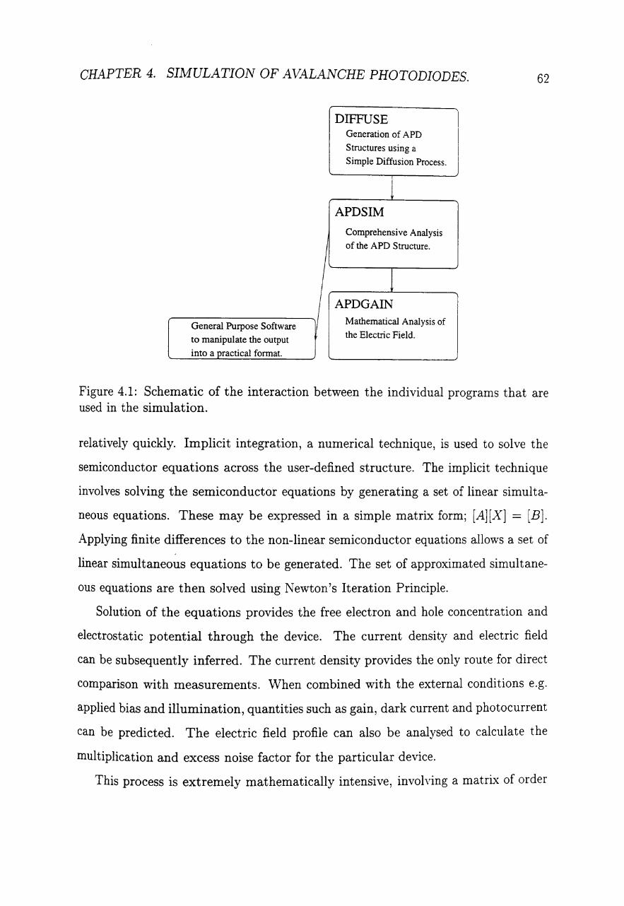
CHAPTER 4. SIMULATION OF AVALANCHE PHOTODIODES. 62
DIFFUSE Generation of APD
Structures using a
Simple Diffusion Process.
1 APDSIM
Comprehensive Analysis
of the APD Structure.
1 APDGAIN
General Purpose Software Mathematical Analysis of
to manipulate the output the Electric Field.
into a practical format.
Figure 4.1: Schematic of the interaction between the individual programs that are used in the simulation.
relatively quickly. Implicit integration, a numerical technique, is used to solve the
semiconductor equations across the user-defined structure. The implicit technique
involves solving the semiconductor equations by generating a set of linear simulta
neous equations. These may be expressed in a simple matrix form; [A][X] = [B].
Applying finite differences to the non-linear semiconductor equations allows a set of
linear simultaneous equations to be generated. The set of approximated simultane
ous equations are then solved using Newton's Iteration Principle.
Solution of the equations provides the free electron and hole concentration and
electrostatic potential through the device. The current density and electric field
can be subsequently inferred. The current density provides the only route for direct
comparison with measurements. When combined with the external conditions e.g.
applied bias and illumination, quantities such as gain, dark current and photocurrent
can be predicted. The electric field profile can also be analysed to calculate the
multiplication and excess noise factor for the particular device.
This process is extremely mathematically intensive, involving a matrix of order

CHAPTER 4. SIMULATION OF AVALANCHE PHOTODIODES. 63
2000 for a typical grid size. The use of a powerful workstation is essential to make
the simulation practical. A Digital ALPHASTATION 233 workstation was employed
to run the software. The length of a typical job was kept down to several days to
produce a full range of bias, illumination and irradiation data.
The following sections will explain each step of the calculation in detail. The
forms of the physical parameterisations will be described and the limitations of the
simulation discussed.
4.2.2 Semiconductor Equations
The semiconductor equations employed in the simulation were in the standard form
(see section 2.2.1):
~ dJ; _ (G - U) = 0 q dx
~ d~ + (G - U) = 0 q dx
(4.1 )
(4.2)
(4.3)
Here r = Nd - Na , and I: NAand I: ND are the ionised deep acceptor and hole
concentrations respectively.
The high grid density in the gain region allowed the assumption that the electric
field was constant over the range of one grid space. This allowed the integral form
of the current equation [80] to be used to increase the stability of the solution in
regions of high electric field [79] inherently present in an APD:
J = - qf.1pE fp(O)eBEX - p(x)] p 1 - eBEx -
( -1.4)

CHAPTER 4. SIMULATION OF AVALANCHE PHOTODIODES: 64
J - q/-lnE [() -BEx ]
n - -1- e-BEx nO e - n(x) . (-1.5)
4.2.3 The One-Dimensional Grid
h'(N) Half-point E ;>
/ x=o x=max 0-----8 • 0 • 0 • 0 0 1 N-l M-l N M N+l M+l N+2 L
/ E ;>
heM) Gridpoint
Figure 4.2: A schematic of the grid composition used in the discretisation of the semiconductor equations.
Finite differences are used to express the semiconductor equations in a linear
form. Application of finite differences involves representing the device structure
as a one-dimensional grid, figure 4.2, each grid-point containing information about
the potential and free carrier concentra~ion. Using half-points for the evaluation of
derivatives is recommended to increase the accuracy of the difference approximation
[79].
A non-uniform grid spacing allows the efficient distribution of grid-points along
the device structure. The high potential gradient in the gain region benefits from
an increased grid density, while the bulk of the device can be adequately discretised
at a lower level. A typical array consists of 2000 gridpoints, 1000 in the first 20% of
the device surrounding the active region and the remaining 1000 spread uniformly
across the final 80% of the device.
4.2.4 Grid Parameter Selection
The design of the grid forms an essential part of the simulation that can often be
overlooked. It usually involves accounting for device specific properties to help fine

CHAPTER 4. SIMULATION OF AVALANCHE PHOTODIODES.
tune the simulation into a working model.
The number of grid points in the simulation determines the overall accuracy
that is attainable. The truncated Taylor expansion is used to derive the spatial
derivatives in the simulation, equation (4.7), and is the dominant source of error.
For a first order approximation the error is of the order of the grid size itself, equation
(4.6) [81].
Error = ~ [~~ f"(x) + ... J (4.6)
Thus reducing the grid-spacing will increase the accuracy of the simulation but at
the expense of increased computation time. At a certain point truncation errors in
the computer will begin to dominate and decreasing the grid-spacing further will
not benefit the accuracy.
The detailed structure of the grid can also be manipulated to improve the accu
racy and convergence properties of a model. A non-uniform grid was investigated due
to convergence problems with the EG&G reverse reach through APD. The selected
grid structure was chosen due to stability of the convergence over a wide range of
incident wavelengths. Several structures were investigated and the 80%/20% split
was found to allow wavelengths in the range 400-800nm to be investigated fully.
Other constructs suffered from non-convergence at either long or short wavelengths.
To select a suitable number of grid points, simulations were run utilising grids
ranging from 500 to 3000 gridpoints. The simulations were performed using a reverse
reach through structure, which is discussed in detail in chapter 5. Figure 4.3 shows
how the calculated potential at one point in the structure varies according to the
number of grid points used in the difference approximation. Table 4.2 outlines the
number of steps and the convergence time .for each size of grid. It is clear from
Fig 4.3 that above 2000 gridpoints the value of the potential begins to stabilise.
The same effect is seen to occur for the carrier concentrations. A large increase
in convergence time, mainly due to extra processing, is seen from 1000 to 2000

CHAPTER 4. SIMULATION OF AVALANCHE PHOTODIODES. 66
gridpoints. A smaller but not insignificant increase in the convergence time is also
observed when increasing from 2000 to 3000 gridpoints. Thus a grid containing
2000 gridpoints was chosen as this appeared to give the best compromise bet\veen
convergence speed and accuracy.
Gridpoints N umber of Steps Convergence Time (s) 500 20 12 1000 12 17 2000 21 52 3000 22 77
Table 4.2: Table showing the convergence steps and time for various grid sizes
<: a;
o.445.....--------r----.....,...-----,-------r----
0.44
0.435 o
0.43
'E 0.425 ~ a..
0.42
0.415 o
0.41
0.405'i?.[)----...l.-----L.-----==~--__;:~----3~000 500 1000 1500 2000 2500
Gridpoints
Figure 4.3: Figure showing the potential variation at one grid point with increasing grid size.

CHAPTER 4. SIMULATION OF AVALANCHE PHOTODIODES. 67
4.2.5 Discretisation Error
As mentioned in the previous section the dominant source of error in the simulation
arises from the granularity of the grid spacing. The finer the grid, the closer the
finite-difference approximation is to the real set of equations being solved. The
accuracy of the solution, for a particular grid spacing, can be set at a very high level
(as is the case here, see section 4.2.9) so that the error in the solution to the finite
difference approximation can be considered negligible. Of course this is just the level
of accuracy to which the approximation has been solved. The level at which the
approximation equates to the real equations determines the overall accuracy, and
this is known as the discretisation error.
Figure 4.4 shows the mean relative shift in the solution across the reverse reach
through structure, for each of the fundamental parameters, as the number of grid
points is increased from 500 to 3000. The plot shows that a finite difference approx
imation using 500 or 1000 gridpoints is clearly too coarse to provide an accurate
solution in this case. The shift from 2000 to 3000 grid points is of the order of a
few percent for the free carrier concentrations, and about 6% for the potential. The
plot indicates that the discretisation error should become negligible between 3000
and 4000 gridpoints, thus we can prudently estimate for 2000 gridpoints, the level
of discretisation error to be of the order of 5% for the carrier concentrations and
10% for the potential.
4.2.6 Application of Finite Differences
To apply the time-independent semiconductor equations to the grid requires that
they are expressed in a discrete form, i.e. discretised. This is achieved by expressing
the spatial derivatives, at gridpoint M, via a truncated Taylor series, equation (4.7).
dp p(N + 1) - p(N) dx (M) = x(N + 1) - x(N)
(4.7)

CHAPTER 4. SIMULATION OF AVALANCHE PHOTODIODES. 68
1d
* Free Holes x Free Electrons 0 Potential
0 x
102
X
:;,g e::: 0 ~ .s:: en (J)
~ CD a:
10' *
* 0
x
10° '--___ -'--___ ~ ___ ___'_ ___ ____"I"'~ __ _____.J
o 500 1 000 1500 2000 2500 Gridpoints
Figure 4.4: Figure showing the mean relative shift in solution for each of the fundamental parameters as the grid size is increased from 500 to 3000 grid points.
Thus a first order difference approximation is used. The discretised equations can
be written explicitly:
q [ 1jJ(N) - 1jJ(N + 1) Jp(M) = h(M) /-lp(M) 1 _ exp-(3(M) p(N) +
(M) 1jJ(N) -1jJ(N + 1) p(N + 1)] (4.8) /-lp 1 _ exp/3(M)
In(M) = q [n(M) 1jJ(N) -1jJ(N + 1) n(N) + h(M) /-l 1 - exp(3(M)
(M) 1jJ(N) -1jJ(N + 1) n(N + 1)] (-J.9) J.ln 1 _ exp-/3(M)
~ J;(M) - J;(M - 1) _ G(N) + U(N) = 0 (-LIO) q h'(N)

CHAPTER 4. SIMULATION OF AVALANCHE PHOTODIODES. 69
1 fn(M) - in(M -1) q h'(N) + G(N) - U(N) = 0 (-tIl)
1 'ljJ (N 1) 1 [1 1 ] h(M - l)h'(N) - - h'(N) h(M - 1) + h(M) 'ljJ(N)
+ h(M)~/(N) 'IjJ(N + 1) = -~ [r(N) + p(N) - n(N)]. ( 4.12)
Here beta(M) is defined as E(M)h(M)8. It should be noted that although deriya
tives are evaluated at half-points, second derivatives, which occur in the Poisson and
continuity equations, are evaluated at the main grid-points.
4.2.7 Linearising the Discretised Equations
Newton's iteration principle is now used to express the equations in a linear simul
taneous form. This involves expressing the true value of each of the fundamental
variables in terms of the present value plus an associated error or increment; e.g.
for the hole concentration:
Ptrue = P~nitial + 5p. (4.13)
the individual terms in the equations are expanded via a truncated Taylor expansion
in terms of the known value and associated increment; e.g. for the hole current
density:

CHAPTER 4. SIMULATION OF AVALANCHE PHOTODIODES. 70
The resulting set of linear simultaneous equations can be expressed as a tri-diagonal
matrix equation:
where;
A(N)8y(N - 1) + B(N)8y(N) + C(N)8y(N + 1)
for 2 < N < MAX - 1
8p
8y(N) = 8n
8'ljJ
and 8y(1) = 8y(M AX) = o.
(-1. 15)
A(N): B(N) and C(N) are 3 x 3 matrices, F(N) is a 1 x 3 vector. N represents the
current position along the grid and MAX the final gridpoint. The matrix equation
is shown in full in appendix A.
4.2.8 Solving the Matrix Equation
Solution of the matrix equation is complicated by its large size. An efficient algo
rithm is required to ensure that processing time is minimised. A method suggested
in [79] is used. This technique involves expressing the matrix equation in terms of
only two grid-points:
B'(N)8y(N) + C'(N)8y(N + 1) = F'(N). ( 4.16)
Thus a reduced set of unknown primed matrices are introduced. A set of recursive
relations can be formed by equating (4.16) to (4.15), re-arranging to give:
8y(N) = B'(N)-lF'(N) - B'(N -1)-lC'(N)8y(N + 1). (.,1.17)
and comparing the resulting equation with (4.16):
CHAPTER 4. SIMULATION OF AVALANCHE PHOTODIODES. 71
B'(N) B(N) - A(N)B'(N - 1)-lC'(JV - 1) (-1.18)
C'(N) C(N) (-1.191
F'(N) F(N) - A(N)B'(N - 1)-lp'(N - 1) ( -1.20)
for 3<N<MAX-l - - .
Using the fact that the endpoints are known via the boundary conditions i.e.
6y(l) = 6y(MAX) = 0
and comparing equations (4.15) and (4.16), uncovers the value of the primed matrices
for N = 2:
B'(2) = B(2) C'(2) = C(2) , P'(2) = F(2)
The recursive relations can now be used to calculate the values of the primed matrices
at each consecutive grid-point. Once the primed matrices are known for each grid
point the value of the incremental matrix ,6y, can be calculated using equation
(4.17) by working back along the grid and again noting that 6y(MAX) = o. Once the values of the vector 6y are known for all gridpoints, the fundamental
variables at each gridpoint can be amended according to (4.13). Thus the solution
of the equations is improved. The non-linear nature of the semiconductor equations
requires that the process be iterated until the solution reaches an acceptable level.
The ultimate accuracy of the final solution is controlled by the order of the difference
approximation and the grid spacing. As shown in section 4.2.4, for a first order
approximation the accuracy that is attainable is typically of the order of the grid
spacing itself. To decide when the required level of accuracy has been reached a
convergence test is applied. This will be discussed in the next section.

CHAPTER 4. SIMULATION OF AVALANCHE PHOTODIODES. 72
4.2.9 Initialising and Terminating the process
The iterative technique described up to this point includes no facility for starting or
ending the process. In order to evaluate each cell in the matrix for the first time~
to initiate the solution process, it is first necessary to have a set of trial values for
n,p and 'l/J. In addition, to terminate the process it is necessary to know when the
solution has reached the required level of accuracy. This is achieved by applying a
convergence test.
Initialisation
To speed the solution process a trial solution that is close to the final solution is
required. Of course, if a trial solution was known for all of the simulated external
influences i.e. bias, illumination and irradiation, then the simulation would have
little value. Thus a simple analytical trial solution is provided for the case with
no external influence. Space charge neutrality is assumed and hence the carrier
densities are given by:
The potential is set to be:
'l/J=
p= l-r n? .:..:J... r
n= lr n? _.:..:J...
r
P region
N region
N region
P region.
~ln ( -11-) P region
Mn ( ~ ) N region.
(4.21)
( 4.22)
( 4.23)

CHAPTER 4. SIMULATION OF AVALANCHE PHOTODIODES. -" I ,)
It is assumed that the device has ideal ohmic contacts i.e. they are in ther
mal equilibrium hence any excess charge immediately vanishes and no space charge
exists. Once a final solution is found, external influences can be gradually intro
duced. The trial solution for the new case is then constructed from the preyious
final solution.
Modifying the Conditions
For a change in applied bias the new trial solution includes the carrier concentrations.
nand p, from the final solution at the previous bias. No alteration is made to the
carrier concentration. Thus it is necessary to step up in small increments of bias.
This ensures that the carrier concentration is not significantly altered by the change
in bias. Typically steps of IV are used.
The electrostatic potential, 'l/J(N) , from the solution at the prevIOUS bias is
slightly altered to provide a new trial electrostatic potential, 'ljJT(N) at each grid
point. This ensures that the boundary conditions are satisfied. A simple propor
tional relation is used to modify the value of 7jJ(N).
[ Vc-Vp] ) Vc-Vp () 'l/JT = 1 - 7jJ(1) _ 7jJ(L) 'l/J(N + 'ljJ(1) _ 'ljJ(L) 'ljJ L ( 4.24)
where Vp and Vc are the previous and current bias, 'ljJ is the electrostatic potential
from the previous solution at the boundaries;(l), (L) and at gridpoint (N).
When simulating neutron irradiation, the complete un-altered solution from the
previous fiuence is used as a trial solution. Thus for the first irradiation the unirra
diated solution is used as a starting point. This method works very efficiently and
steps of 1 x l013ncm-2 are possible.
The software is designed to produce data over a pre-set range of bias and neutron
irradiation fiuence, for a particular device, with the minimum of user interaction.
This is necessary as the simulation can run for several days. The efficient storage
and retrieval of 'old' solutions is clearly essential as these form part of later solutions.
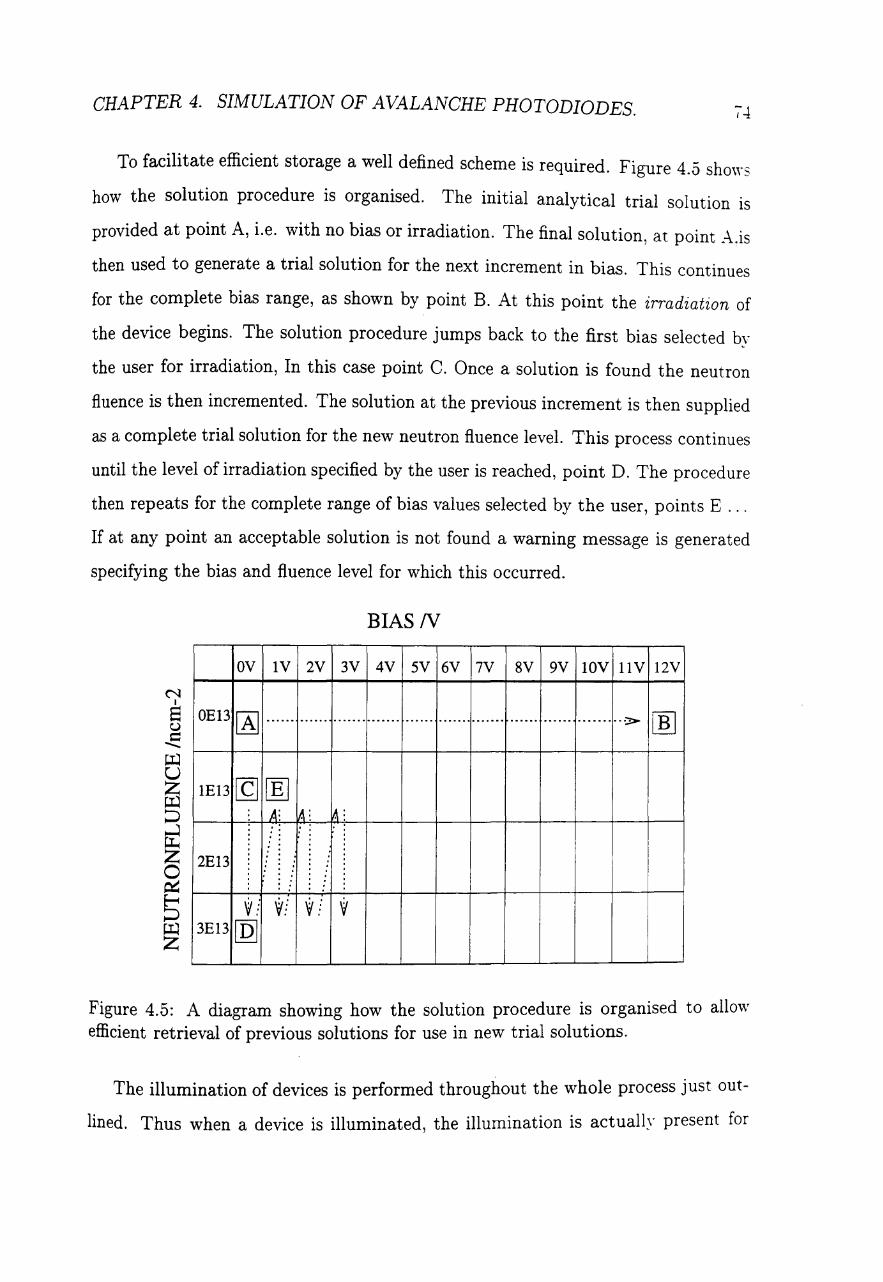
CHAPTER 4. SIMULATION OF AVALANCHE PHOTODIODES. 7-1
To facilitate efficient storage a well defined scheme is required. Figure 4.5 shmys
how the solution procedure is organised. The initial analytical trial solution is
provided at point A, i.e. with no bias or irradiation. The final solution, at point A.is
then used to generate a trial solution for the next increment in bias. This continues
for the complete bias range, as shown by point B. At this point the irradiation of
the device begins. The solution procedure jumps back to the first bias selected by
the user for irradiation, In this case point C. Once a solution is found the neutron
fiuence is then incremented. The solution at the previous increment is then supplied
as a complete trial solution for the new neutron fiuence level. This process continues
until the level of irradiation specified by the user is reached, point D. The procedure
then repeats for the complete range of bias values selected by the user, points E ...
If at any point an acceptable solution is not found a warning message is generated
specifying the bias and fiuence level for which this occurred.
BIASN
OV IV 2V 3V 4V 5V 6V 7V 8V 9V lOV llV 12V
DE 13 ~ ....... ...... ........ ......... ...... ........ ....... ...... ...... ......... ... > [ID
IE13 [Q [gJ : A .,i: ~: . . . . ..
: : : : : : :
2E13 : : : : : :
: :
Vi Vi vi 'VI 3E13 [2]
Figure 4.5: A diagram showing how the solution procedure is organised to allow efficient retrieval of previous solutions for use in new trial solutions.
The illumination of devices is performed throughout the whole process just out
lined. Thus when a device is illuminated, the illumination is actually present for

CHAPTER 4. SIMULATION OF AVALANCHE PHOTODIODES. Iv
the first scenario with no bias or neutron irradiation. The analvtical trial solution
given by equations (4.21), (4.22) and (4.23), is also used with illumination. Thus
to characterise a device for several wavelengths over a range of bias and irradia
tion conditions, a set of processes is required. One un-illuminated process provides
the dark current at each bias and neutron fiuence and the illuminated processses
are used to provide the photo currents at selectable wavelengths. In this way the
spectral response of the device can be evaluated for any combination of bias and/or
neutron fiuence.
Termination
A convergence test is used to determine when the solution has reached the required
level of accuracy. The absolute error in the solution cannot be determined explicitly
because the true solution is unknown. Thus a new parameter, the residual, is used
as a measure of the relative error at each gridpoint. The residual is defined as
the ratio between the calculated increment, i.e. fJp, used to modify the value of
the fundamental variable and the value of the fundamental variable itself i.e. p.
Defining the residual such that the relative error is used allows a single threshold to
be applied equally to each variable at each grid point. Once the required threshold is
reached at each gridpoint the iteration is terminated. Typically a value of 5x10⁻⁹ is
used as this is typically the minimum that can be achieved for the first few solutions.
4.2.10 Impact Ionisation
Impact ionisation is the fundamental process that underlies the operation of avalanche
photodiodes, thus inclusion of the process is essential. A generation term that de
scribes impact ionisation is incorporated into the continuity equations (4.1),(.1.2):
(.L2.S)
The electron and hole ionisation rates in silicon, lle and llh. are calculated using a
modified [82] form of the Baraff three parameter theory [83]. equation (.-1.26).
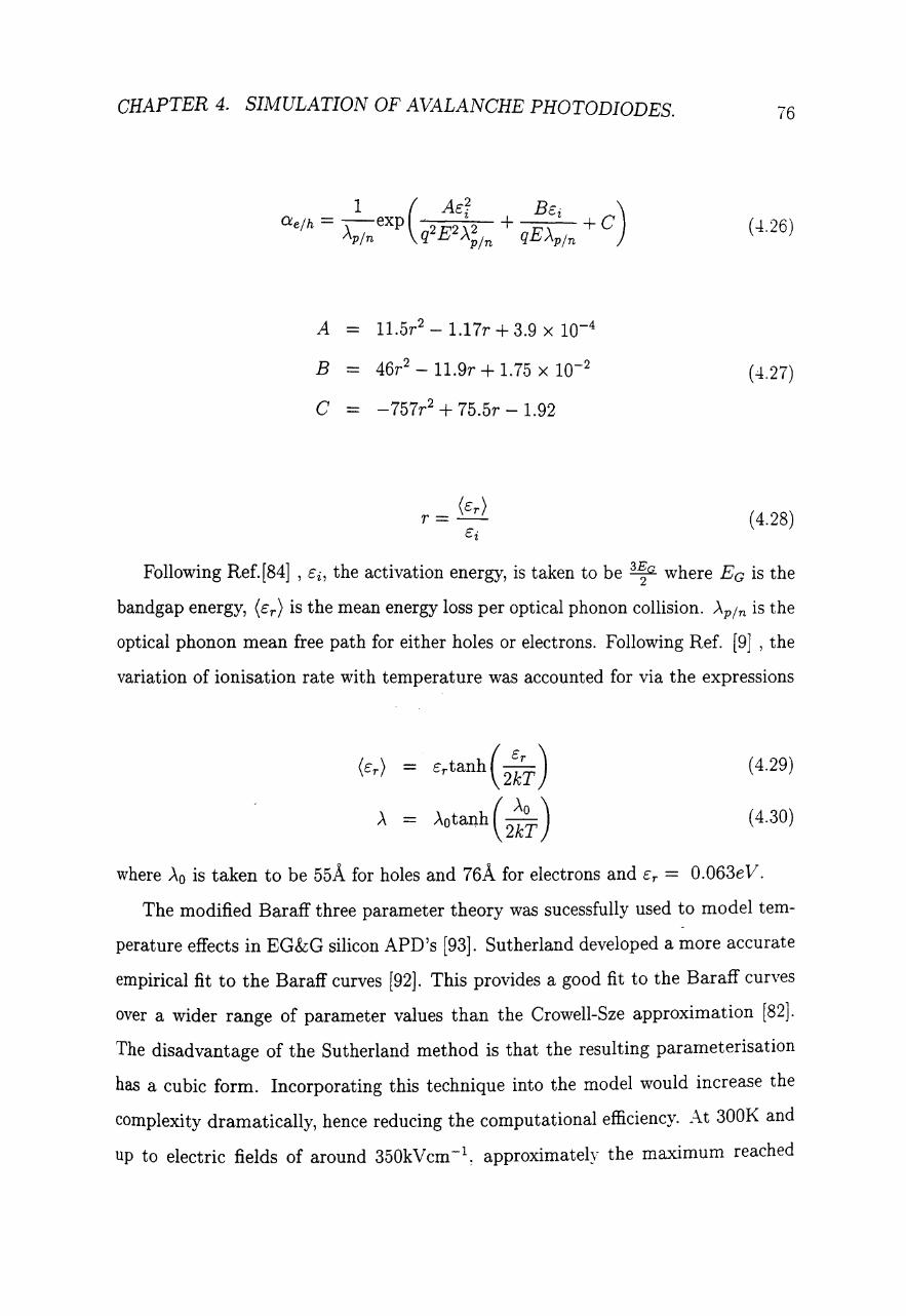
CHAPTER 4. SIMULATION OF AVALANCHE PHOTODIODES. 76
(-1.26)
A l1.5r2 - l.I7r + 3.9 x 10⁻⁴
B 46r2 - 11.9r + 1.75 x 10⁻²
( 4.27)
C -757r2 + 75.5r - 1.92
( 4.28)
Following Ref. [84] , Ci, the activation energy, is taken to be 3~G where Ec is the
bandgap energy, (cr) is the mean energy loss per optical phonon collision. Ap / n is the
optical phonon mean free path for either holes or electrons. Following Ref. [9J , the
variation of ionisation rate with temperature was accounted for via the expressions
(or) Or tanh C~T ) ( 4.29)
A = AO tanh C~~ ) ( 4.30)
where Ao is taken to be 55A for holes and 76A for electrons and Cr = 0.063eV.
The modified Baraff three parameter theory was sucessfully used to model tem
perature effects in EG&G silicon APD's [93]. Sutherland developed a more accurate
empirical fit to the Baraff curves [92]. This provides a good fit to the Baraff curves
over a wider range of parameter values than the Crowell-Sze approximation [82].
The disadvantage of the Sutherland method is that the resulting parameterisation
has a cubic form. Incorporating this technique into the model would increase the
complexity dramatically, hence reducing the computational efficiency. At 300K and
up to electric fields of around 350kVcm-l, approximately the maximum reached

CHAPTER 4. SIMULATION OF AVALANCHE PHOTODIODES. --j j
by the models, the less complex Crowell-Sze approximation performs well. The
improvement offered by the Sutherland model, over the Crowell-Sze method. oc
curs predominantly at higher electric fields than found in the models developed.
and would incur a large computational penalty. Hence the use of the Crowell-Sze
approximation is preferable due to its relative simplicity.
The generation term is evaluated at the main grid point and hence the current
density and electric field, which are evaluated at the half-points, have to be trans
formed to main grid points also. To increase the accuracy of the generation term,
this is achieved by assuming a linear change in their values between the half-points
and therefore the value at the main grid-point is taken to be the mean of the two half
point values weighted to the distance between the half-points and the main-points,
figure 4.6. The weighting is necessary for regions of non-uniform grid-spacing. The
electric field and hole current density at the main-points are written explicitly in
equations ( 4.31) and (4.32).
E(N) = hl(~) [h(~) h(MI_I) [1j!(N) -1j!(N - I)J +
h(M - 1) 1 [7jJ(N 1) - ?jJ(N)l] 2 h(M) +
h(M) q [ ?jJ(N - 1) - 7jJ(N) N _ 1 + Jp(N) = 2h'(N) h(M _ 1) J-lp(M - 1) 1 _ e-8[W(N-l)-W(N)]P( )
7jJ(N - 1) - 7jJ(N) ] J-lp(M - 1) 1 _ e8[7fJ(N-l)-W(N)]p(N) +
h (M - 1) q [ M?jJ (N) - ?jJ (N + 1) N + 2h'(N) h(M) J-lp( ) 1 - e-B[w(N)-w(N)] p( )
7jJ(N) - ?jJ(N + 1) N 1] J-lp( M) 1 _ eB[7fJ(N)-w(N +1)] p( +)
(4.31)
( 4.32)

CHAPTER 4. SIMULATION OF AVALANCHE PHOTODIODES: 78
Equation (4.33) shows the generation term in its explicit form.
G(N) = ~ [ :n exp {
C (wVvi- [~h(,J-1) ['IjJ(N) - 'IjJ(N - l~]e: h(~-l) ~['IjJ(N + 1) - 'IjJ(N)]]) \~) (
Bc· ) + e (h,r'N) [h(~) h(,J -1) ['IjJ(N) - 'IjJ(N - 1)1 : h(~ -1) h(~) ['IjJ(N + 1) - 'IjJ( N)]]) An
_ c} X { h(M) q [ _ 7jJ(N - 1) - 7jJ(N) 2h'(N) h(M - 1) J-Ln(M 1) 1 _ e8[7P(N-l)-7P(N)] n(N - 1) +
7jJ(N - 1) - 7jJ(N) ] /1n(M - 1) 1 _ e-8[7P(N-l)-7P(N)] n(N) +
h(M - 1) q [ 7jJ(N) - 7jJ(N + 1) 2h'(N) h(M) J-Ln(M) 1 _ e8[7P(N)-7P(N)] n(N) +
7jJ (N) - 7jJ (N + 1) ] } 1 { J-Ln(M) 1 _ e-8[7P(N)-7P(N+l)] n(N + 1) + Ap exp
( Ac~ )
e2 (hllN) [h(~) h(~-l) [~(N) - 7jJ(N - 1)] + h(~-l) h(~) [7jJ(N + 1) - 7jJ(N)]] ) 2 A~
( Bc· )
+ e (h'('N ) [h(~) h(,J -1) ['IjJ(N) - 'IjJ(N ~ 1)] : h(~-l) h(~) ['IjJ( N + 1) - 'IjJ(N)] 1 ) Ap
}. {h(M) q [ 7jJ(N - 1) - 7jJ(N)
- C X 2h'(N) h(M _ 1) J-Lp(M - 1) 1 _ e-8[7P(N-I)-7P(N)]p(N - 1) +
7jJ(N - 1) - 7jJ(N) ] /1p(M - 1) 1 _ e8[7P(N-I)-7P(N)]p(N) +
h(M - 1) q [ 7jJ(N) - 7jJ(N + 1) 2h'(N) h(M) J-Lp(M) 1 _ e-8[7P(N)-7P(N)] p(N) +
7jJ (N) - 7jJ (N + 1) } ] ] J-Lp(M) 1 _ e8[7P(N)-7P(N+l)] p(N + 1) (4.33)
4.2.11 Illumination
A change in incident wavelength can have several independent simultaneous effects
on a device's operation. The net effect can appear extremely complex over a range

CHAPTER 4. SIMULATION OF AVALANCHE PHOTODIODES.
h'(N)
x=o ~h(~-l) + _h(~_) 1 x=max
G- -- - -er---1 • .....---~O:r-------.,._--~O~--a.~-O 1 N-l M-l ......... ;:J"N M N+l M+l L
... ... ... ...
... ... ...
... ... E
E(N) = heM) E(M-l) + h(M-l)E(M)
2h'(N) 2h'(N)
heM)
Figure 4.6: A figure showing the method used to transform the electric field from the half-points to the main grid points.
of wavelength and bias. To simulate accurately the spectral response of a device~ in
particular an APD, it is necessary to include illumination directly into the model.
Thus the simulation automatically superimposes the different effects that can occur.
In this way the simulated diode can be illuminated and tested using a process that
relates directly to experimental method.
Monochromatic illumination is included via a generation term in the continuity
equations. Normal incidence is considered at all times.
G(N) = e-(3x(N) _ e-(3x(N+l) (4.34)
Equation (4.34) shows the form of the generation term used. Here f3 represents the
optical absorption co-efficient in silicon. The signal charge generated at each grid
point represents the integrated charge generated over the whole inter-grid point spac
ing. The variation in optical absorption co-efficient with wavelength in silicon,(4.35),
is described using data from [85].
(4.35)

CHAPTER 4. SIMULATION OF AVALANCHE PHOTODIODES. 80
During the simulation one job is left to run without illumination, producing
dark current data and several illuminated jobs are run to produce data at each
wavelength. The data produced in this way are identical in form to the data collected
experimentally. This simplifies the evaluation of the data as the same manipulation
is applied to both data sets.
4.2.12 Neutron Radiation Damage
The main motivation behind the development of the simulation was to investigate
the effects of neutron radiation damage in avalanche photo diodes. Neutron radiation
damage was incorporated into the model via the introduction of deep acceptor levels
and a suitable change in the minority carrier lifetime. This method was sucessfully
used to model the change in Neff with neutron fiuence in silicon microstrip detectors
[86].
The deep acceptor levels are included via a term in the Poisson equation (4.3).
The total number of filled acceptors at grid point N , L N A (N), is given by the
product of the total number of available levels, NA(N) and the occupancy function,
f(ET,N), equation (4.36).
( 4.36)
A Shockley-Read-Hall occupancy function is used to fill the deep levels. The fraction
of filled acceptors, at energy ET and gridpoint N, is given by equation (4.37).
f (ET
, N) = n( N) + ~p( N) + niexp ( E'k;:' E') + ~niexp ( E';i'T ) ( 4.37)
Initially quasi-Fermi statistics were used to describe the occupancy of the deep
levels; this equates to substituting (Jp = 0 in equation (4.37). The use of quasi-Fermi
statistics resulted in severe convergence problems. This was thought to be due to the

CHAPTER 4. SIMULATION OF AVALANCHE PHOTODIODES. 81
lack of consideration of electron emission, via (Jp, causing the occupancy function to
saturate when the deep donor implant in the reverse structure was partly depleted.
The most likely candidate for the deep acceptor level is the "20 complex [87],
[88] which is situated O.5eV below the conduction band (see chapter 3). The deep
acceptor level used in the simulation is based on the V20, although any species
of acceptor or donor level can be modelled. A maximum of one acceptor and one
donor level is possible. The V20 introduction rate, for 1 MeV neutrons, has been
calculated from a defect kinetics model to be O.96cm-1 at 20°C [88]. A summary of
the properties of the deep level used in the simulation are provided in table 4.3
Property Value Name V20 Type Acceptor Charge Un-occupied neutral Charge Ionised negative (-1) Position Ec - O.5eV Introduction Rate O.96cm- 1at20°C !!.P.. Un
1
Table 4.3: Table showing the properties of the deep acceptor level used in the simulation.
The variation in minority carrier lifetime, 7, with neutron fiuence, <I>n in sil
icon under equilibrium conditions, is described in terms of the lifetime damage
constant,Kr [89]:
1 1 <Pn -=-+-. 7 70 Kr
For high fiuences this can be written as:
1 <Pn -~-7 K r ·
( 4.38)
( -1.39)
The minority carrier lifetime in the simulation is varied according to (-1.39) and
it is assumed that the effective carrier lifetime in the depletion region is subject to

CHAPTER 4. SIMULATION OF AVALANCHE PHOTODIODES. 82
the same relation. The value of Kr is calculated for high resistivity-silicon [89] to
be approximately Kr = 107scm-2. With Kr set to this value the rate of change of
Neff with fluence is kept consistent with predictions [87], [89] by setting the ratio of
the hole and electron capture cross-sections to unity [87]. The introduction of the
deep acceptor levels is assumed to be linear with neutron fiuence.
The effects of annealing, although extremely important in the overall under
standing of device performance under irradiation, have not been included in the
model. This would be a very worthwhile extension to the model but there exist only
limited data on the annealing of the concentration of individual defect species, in
particular the V 20. This information would be needed to modify the defect concen
tration with time. It would also be necessary to calculate how the minority carrier
lifetime should be modified with annealing.
4.3 APDGAIN
4.3.1 Introduction
The multiplication factor is defined as the multiplying power of the gain region. For
example if an electron is injected into a gain region with a multiplication factor of
Me = 10, then 10 electrons will emerge. Similarly we can define a hole multiplication
factor M h . If an electron is generated inside the gain region it will experience less
multiplication, i.e. Me < 10.
The current gain calculated from APDSIM includes effects such as absorption
of signal charge in the gain region. Thus inferring the multiplication factor from
the data can be difficult. To evaluate the multiplication factor directly an analysis
is performed on the electric field profile provided by APDSIM. This allows the
multiplication factor of the gain region to be computed and compared with the
current gain evaluated directly from APDSIM. A simple extension of this process
also allows the excess noise factor of the device to be evaluated.
CHAPTER 4. SIMULATION OF AVALANCHE PHOTODIODES. 83
4.3.2 Multiplication Factor
To calculate the multiplication factor equation (4.41) is evaluated across the gain
region, this follows from the equation 2.41. Only the electron multiplication factor
is calculated as most silicon devices are primarily designed to multiply the electron
signal (see section 2.3.6). The multiplication factor is defined as
1 Me=--
I-I ( -1.40)
Where
(-1.41)
To determine the bounds of the gain region, the ionisation co-efficients are evaluated
across the whole device using a simple Chenowyth approximation (see section 2.3.5).
The boundaries of the gain region are then defined as the points at which the electron
ionisation rate, ae , becomes greater than unity.
Once the gain region has been specified, the number of grid points describing the
electric field in the gain region is dramatically increased. Typically 50 grid points
are introduced between the existing grid points. This is achieved by assuming a
linear change in the electric field between the grid points and simply assigning the
value of the new points accordingly.
Equation (4.41) is now computed across the magnified region. The integrals are
evaluated using the trapezoid rule. To remain consistent with APDSIM during the
calculation the ionisation co-efficients are expressed via the modified Baraff three
parameter theory [83] . When the calculation is complete the magnification process
is repeated, with another 5 grid points being inserted. Equation (4.41) is evaluated
again and this process repeated until the change in the result falls below a pre
determined level, typically 1 x 10⁻³ . This corresponds approximately to an error of
1 % on a gain of 10 and 10% on a gain of 100.

CHAPTER 4. SIMULATION OF AVALANCHE PHOTODIODES. 84
4.3.3 Excess Noise Factor
Discussion of APD properties is incomplete unless some mention of the excess noise
factor is included. The discussion in chapter 2 explains that the excess noise factor
is inherent in a device such as an APD, with a statistical gain mechanism. To this
end a simple analysis of the excess noise factor was incorporated into the model [33].
( 4.42)
The excess noise factor is calculated using equation (4.42). The equation is
similar to the form introduced in chapter 2 but the variation of the ratio of the
ionisation co-efficients, k, with the electric field is accounted for in the term Keff .
The definition of Keff is given in equation (4.43), where the terms kl and k2 are
defined in equations (4.44) and (4.45) respectively. The electron excess noise factor
is calculated for the same reasons outlined in section 4.3.2.
( 4.43)
( 4.44)
Jow ahM(x)2dx k2 = ~w.,....-----
Jo aeM(x)2dx (4.45)
The calculation of the excess noise factor is incorporated into the calculation of
the multiplication factor. This is possible because they are both calculated from
the same common components. The magnification discussed in section 4.3.2 is also
applied to the calculation of the excess noise factor. The process is terminated using
the same conditions outlined in section 4.3.2.

CHAPTER 4. SIMULATION OF AVALANCHE PHOTODIODES. S.3
4.4 DIFFUSE
4.4.1 Introduction
The final piece of software, DIFFUSE, is used to create the one-dimensional doping
profiles of the devices under investigation. The aim of the software is to allow a user
to specify the peak concentration and depth of the specific implants and to generate
a structure accordingly.
The implants were created using a simple drive in diffusion process. This process
consists of diffusing a fixed amount of dopant into the substrate and is a reasonable
approximation of the method used to create the EG&G devices under investigation.
The dopants used are phosphorus for the n-type implants and boron for the p-type
implants. Phosphorus and boron are typical dopants used in silicon due to their
high solubility, typically above 5 x 10²ocm-3 [90]. It is assumed for simplicity that
the diffusion co-efficient of phosphorus and boron are unchanged even when diffusing
through already heavily doped regions.
The diffusion process is described by Fick's diffusion equation (4.46).
8C _ D82C Tt - 8x2
( 4.46)
The solut'ion of the equation satisfying the boundary conditions for drive in diffusion
equations (4.47) and (4.48), is given by equation (4.49).
[" C{x, t)dx = 1
C(oo, t)dx = 0
S x 2
C(x, t) = J7i15texp [ - 4Dt J 7rDt
( -1.47)
( -1.48)
( -1A9)

CHAPTER 4. SIMULATION OF AVALANCHE PHOTODIODES. 86
Once the user's parameters are set, the program steps up in time calculating the
concentration profile of each of the implants, until each implant reaches the required
specifications. Once an individual implant is deemed satisfactory~ its diffusion is
stopped and the remaining implants allowed to continue. When the last implant
is successfully diffused the process is terminated and the doping profile is sa'"ed
to a file. The diffusion co-efficients used in DIFFUSE are 3.0 x 10⁻¹²cm28- 1 for
phosphorus and 4.5 x lO-12cm28 - 1 for boron after Ref [91].
4.5 Simulation Limitations
4.5.1 Introduction
A detailed summary of each of the three pieces of software used in the simulation
has been presented. Once supplied with an effective doping profile the suite of
software can be considered a model. To complete the summary a list of the key
assumptions/limitations are listed.
4.5.2 APDSIM
• A one dimensional form is useful for investigating the bulk properties of a
device i.e. dark current or effects due to variation of light absorption in the device.
The significant limitation of a one-dimensional model is that surface effects and
non-linearities along the lateral direction, which may result in impact ionisation
occurring outside the defined gain region, have to be ignored. In a real device these
play a significant part of the operation .
• The Crowell-Sze parameterisation of the universal Baraff curves that is used
to calculate the ionisation rates in silicon has been shown to be inaccurate in some
circumstances. Sutherland [92] discussed this problem and generated a cubic pa
rameterisation that gave better coverage of the Baraff curves over a wider range of
temperature and electric field strength. The data presented in this model are at
300K and the field strengths do not rise far above 350kl"cm-1. In this domain the

CHAPTER 4. SIMULATION OF AVALANCHE PHOTODIODES. 87
relatively simple Crowell-Sze approximation performs well. The implementation of
the Sutherland parameterisation would be extemely complex, and the computational
time would increase accordingly. Thus the use of the Crowell-Sze approximation is
justified here but inclusion of the Sutherland parameterisation would be useful to
expand the range of conditions accurately available to the model.
• The effects of self heating in the diode are not included in the model. In
avalanche photodiodes this can become a very important effect as the gain can Yary
significantly with temperature. The inclusion of self heating would be a significant.
step in the path to creating an extremely versatile model.
• The parameterisation of the mobility, which accounts for the variation of the
carrier mobility with, carrier concentration, is not dependent on the temperature.
This provides a major limitation to investigation of temperature dependent effects.
To extract the full potential of the model a more general parameterisation needs to
be developed.
• No account is taken of annealing of the radiation damage. The effects of
annealing are of equal importance to the initial effects of radiation damage: as
most devices are operated in conditions where annealing is present. A worthwhile
extension to the model would be to include these effects. In order to do so, more
specific information will be required about the change in concentration of individual
defect species, e.g. V20, during annealing. Also the effect of annealing on the
minority carrier lifetime will have to be investigated .
• The introduction of the neutron induced recombination centres is assumed to
be linear with neutron fiuence. This is a valid assumption as the measured increase
in dark current due to the introduction of recombination centres, is seen to increase ,
linearly with neutron fluence indicating a linear increase in the trap density.
4.5.3 APDGAIN
• The limitations of the Crowell-Sze Baraff parameterisation apply here also.
The use of a more sophisticated parameterisation would allow accurate simulation

CHAPTER 4. SIMULATION OF AVALANCHE PHOTODIODES. 88
over a wide range of temperature and with very large electric fields in the aain b
region.
• The multiplication factor and the excess noise factor are calculated in terms
of an injected electron current only. This is valid as most, if not all, silicon devices
are designed to multiply only the electron signal in an attempt to reduce the excess
noise factor.
4.5.4 DIFFUSE
• The main assumption is that the diffusion of the implants is taken to be
independent of the concentration of dopants already present in the substrate. This
is an acceptable assumption in silicon as the diffusion is generally not sensitive to
the dopant concentration [9].
4.6 Conclusions
A sophisticated simulation package has been introduced and the key components of
its operation explained in detail. A full summary of the limitations and assumptions
relating to each package has been given. A short description of the process of running
the simulation is given in appendix B.
To conclude, the simulation is a very complex attempt at providing a realistic
simulation of avalanche photodiode properties both before and after neutron irradi
ation. There exist several avenues for improvement which will allow the simulation
to provide a significantly improved performance.

Chapter 5
Results
5.1 Introduction
The complementary APD designs used for the simulation were introduced in chapter
2. The reach through APD is designed to operate in the range 400-1100nm. The
reverse reach through APD is a modified form of the standard reach through APD,
optimised for scintillation applications, and operates in the range 400-700nm. The
reach through APD has a wide depletion region in front of the gain region. This
gives rise to a high quantum efficiency over a wide range of incident wavelengths.
Conversely, the reverse reach through structure has a narrow depletion, in which
light is collected in front of the gain region. This trades the high quantum efficiency
at the longer wavelengths for a reduction in the nuclear counter effect.
Implant S Icm-2 t Is Peak Level Depth Icm-3 I f-Lm
p+ 1 X 101::1 5 3 X 101r 0.12 p 2.4 x 10¹³ 22386 6 x 10¹⁵ 17.5
n+ 3.4 x 10¹⁴ 511 7 x 10¹⁷ 5.0 7r - - 2.5 X 10¹² -
Table 5.1: Table showing the specifications of each of the diffused implants used to
create the reach through model.
The doping profiles used in the simulation are shown in figures 5.1 and 5.2 for the
reach through and reverse reach through structures respectiYely. Light entry is fu
89

CHAPTER 5. RESULTS 90
Implant S lem -2 t Is Peak Level Depth lem-3 I j.lm
p+ 1 x 10¹³ 5 3 X 10¹⁷ 0.12 p 9.4 x 10¹³ 4481 5 x 10¹⁶ 8.9 n 4.3 x 10¹³ 50206 8 x 10¹⁵ 22.0 n+ 1 x 10¹⁴ 30 6 X 10¹⁷ 1.0 7r - - 2.5 X 10¹² -
Table 5.2: Table showing the specifications of each of the diffused implants used to create the reverse reach through APD model.
the left for both figures. The generation of the doping profiles is discussed in chapter
4. The parameters used to generate the doping profiles for the reach through and
reverse reach through models are given in tables 5.1 and 5.2 respectively.
\
10'6~ \
14 \ I -- Phosphorus I " " 10 I . - - - Boron . /
\ I
10'2
l ______________________________ 1
i
100 L-_I...-_I...-_I...-_..1-.-_...I.--_...I.--_..1-.-_.L-_I...-L-.-J
o 10 20 30 40 50 60 70 80 90 100 Depth 111m
Figure 5.1: Doping profile used to simulate a silicon reach through APD.
The development of both models followed the same path. Initially literature
regarding the structure was investigated. Once a working model was created i.e. a
model which provided good convergence characteristics over the whole range of bias.
illumination and neutron irradiation being investigated, the implants were adjusted
until the general performance of the model matched the reported operation. The

CHAPTER 5. RESULTS
10'8 r ---.-----r----,r-__ ...,-__ -.-__ _
" \ \
\ \
I~ Phosphorus Boron
\_- - - - - - - - - - - - - - -----------
10° :-----:l:------J..-....l-----J'----__ ...l....-__ ....I.-__ .J. o 20 40 60 80 100 120
Depth 111m
91
Figure 5.2: Doping profile used to simulate a silicon reverse reach through APD.
latter part of the process proved particularly time consuming. This was not only
due to the extreme sensitivity of the device performance to the internal structure
but also because modifying a working model often generated one where the solution
diverged. Finding a structure that reasonably matched the experimental properties
and had good convergence properties proved extremely difficult.
The limited supply of information regarding the structures of the devices signif
icantly reduced the ability of the models to provide quantitative predictions. Thus
the aim of the experimental study was limited to providing qualitative comparison
with the predictions made by the model.
5.2 Pre-Irradiation
5.2.1 Introduction
The experimental study was performed on two EG&G devices, the C30916E reach
through APD and the C30719E reverse reach through APD. The results presented
here are divided into two key regions; pre-irradiation and post-irradiation. The aim

CHAPTER 5. RESULTS 92
of the results is to demonstrate the wide range of information that can be extracted
from the models, ranging from detailed microscopic information to the investigation
of macroscopic phenomena.
5.2.2 Microscopic Features
The advantage of implementing a full drift-diffusion formulation without making
broad assumptions, such as the depletion approximation, is that the device can
be investigated throughout the full bias range. The microscopic properties of the
devices, i.e. free carrier concentration, potential and electric field, are investigated
over a wide range of bias. Figures 5.3 and 5.4 show how the hole and electron
concentration vary with applied bias for the reach through structure.
10'8
10'6 Nh 50V
Nh 100V Nh 200V
10'4 Nh 300V
10'2 ~ ~
('I) :.
Ie ~ ~ 10'0 ~ .2 l a; i 11~ ~ I u . . 8 '( ......................................................................................... ; ...... .
106
- . __ . -. -- ._. __ .- • __ • _. __ ._.- _. - • __ . - • __ . _. --. _. -------, -,.
I (
"
100
OL--1.L...0 --2.L...0 --3.J....0--4.J...0---:l:50~--:60:----:7:-0 ---;:8:;;-0 ---;:90:;--;-;:100
Depth 111m
Figure 5.3: Variation in free hole concentration with bias for the reach through model.

CHAPTER 5. RESULTS
- N 50V • N 100V • N 200V • N 300V •
,----------------------------106 I
10' <",. .•. ~ ...... ~ ......... .,., ~ ......... .., ~ ••. .,. ... ,.., M.,-.··.,., •••. ~.'" ........ ," ........ ," ........ ," '" ~"" \.\
" \ / "
102 J
1
1 00 :----:":----:~---::1:--~~:______:"----L.-----J..---'--..J o 10 20 30 40 50 60 70 60 90 100
Depth 111m
93
Figure 5.4: Variation in free electron concentration with bias for the reach through model.
Up to lOOV the depletion is limited to the highly doped gain region. Once the
lightly doped 7r region is reached, depletion occurs much more rapidly, until the
device is fully depleted. Full depletion has occured by 200V. At 300V the gain of
the device is large and a large injection of holes from the gain region into the device
is visible.

CHAPTER 5. RESULTS
'" 'E
~ 1010
o 'e ~ 10· c: 8
106
.... , \
\
\
\
.. '" ~ ~.'.':'"'. ',:-: :-.".-:-. ':""': :a.'.-:-,',,!,,,,:,..
Nh 110V Nh 120V Nh 130V Nh 140V
.... , \
\
\
\
1if~--~--~--~--~--~----~--~---L--~ __ ~ o 10 20 30 40 50 60 70 80 90 100 Depth/J.lm
9-1
Figure 5.5: Variation in free hole concentration with bias for the reach through model as the device undergoes reach-through.
N 110V • N 120V • N 130V • N 140V •
L II I
100~ __ ~ __ ~ __ ~ __ ~ __ ~ ____ ~ __ ~ __ -L __ ~ __ ~
a 10 20 30 40 50 60 70 80 90 100 Depth/J.lm
Figure 5.6: Variation in free electron concentration with bias for the reach through model as the device undergoes reach-through.
The transition of the depletion from the highly doped p-region to the lightly

CHAPTER 5. RESULTS 95
doped 7r region is known as 'reach-through' and has a significant effect on the macro
scopic device properties [94]. Figures 5.5 and 5.6 show the change in the hole and
electron concentration as the reach through APD undergoes 'reach-through'. The
spread of the depletion region across the device is clearly visible.
350 r---;:::::::::=:::::!=:::::::;~=:;::::::;--'----'---'---r---r---:- 350
Electric Field (50V) I ' 300
250
,. 200
~ "0 C6 150 i! CJ
'1:
~ 100
50
-Electric Field (300V)
Potential (50V) I If 300 Potential (300V) ~~
1: 250 ; : f.! /: ~ 200
I : It / :!t ~
~., : ,- (ij " . ~ ~ .-
, ... ' :!1150~ ",..- =,' 0:
" :.! ~ ,~ . I'
, ~' : ; ! 100 .,,' :.1
_~~-~~-~~-~~ . .l!i) > ......... ".#r .......................................................... ........ _......... "
o .... ~ . i 0
-SO '--_..L-_....I..-_....l.-_---I-_--l..._----l._---L_----"_----l_---l -50 o 10 20 30 40 50 60 70 80 90 100
Depth/~m
Figure 5.7: Variation in potential and electric field across the reach through model at 50V and 300V.
Figure 5.7 shows the relationship between the potential and the electric field
across the device both before and after the device is fully depleted. The peak
electric field region, that constitutes the gain region, is clearly visible. Once the
device has 'reached through' and is fully depleted a large fraction of the potential
drop is across the 1f region. This reduces the sensitivity of the peak electric field~
and hence the gain, to fluctuations in the applied bias.
The free hole and electron concentrations through the reverse reach through APD
are shown in figures 5.8 and 5.9. 'Reach-through' occurs at a much higher bias than
for the reach through structure. The device is fully depleted at 300\'~ like the reach
through APD the depletion region extends through the majority of the device.

CHAPTER 5. RESULTS 96
1018
I
1016 - Nh 50V j
Nh 100V J Nh 200V
1014 i Nh 300V
1
1 10
12 i ~ j E ;
..!:! 1010 ! § 1 e i ~ 108 i u c: 0 U
106
............ . .....
10'
102
100
0 20 40 60 80 100 120 Depth fJ.lm
Figure 5.8: Variation III free hole concentration with bias for the reverse reach through model.
1018 ,------,.---------r-----T----,-----.,....------,
1 i··· t ··
1 1
20 40
N 50V • N 100V • N 200V • N 300V •
- --.- - .. - -- -. ~. - .. - -. - -.-
60 Depth fJ.lm
80 100 120
Figure 5.9: Variation in free electron concentration with bias for the reverse reach through model.

CHAPTER 5. RESULTS
10'81 -----.----.----.---_-,-___ ...--__ _
I I
/
/
,,'- , \
- .... -.- ..
" , \
\
\ \
\
\
\
. '" . -:-: :-:,":'".' :- - -
Nh 210V
Nh 220V
Nh 230V
Nh 240V
.. ---:--~
10° ::------:.:------:1:----..L------I.----'--__ .-.J o 20 40 60 80 100 120
Depth/J.lm
9~
Figure 5.10: Variation in free hole concentration with bias for the reverse reach through structure as the device undergoes reach-through.
10'8,------.----.----..-------..----...------,
, ,",
, I ' , \
" ' , ' , , ' I!
"
\
N 210V • N 220V • N 230V • N 240V •
---
40 80 100 120
Figure 5.11: Variation in free electron concentration with bias for the reverse reach through model as the device undergoes reach-through.
Figs. 5.10 and 5.11 show how the reverse reach through APD 'reaches though'.

CHAPTER 5. RESULTS 98
The depletion spreads into the 7r region from each of the ends. This is unlike the
reach through APD, where the depletion extends only from the pn junction at the
rear of the device. 'Reach through ' occurs in this device when the depletion region
at the rear of the device spreads into the 7r region.
~:----'------;----r-----'----r---~ 350
I ....•. • 0'
'I E
I .'
1/ F .1 ~ 150
'" I': I :2 . ~ 11\: I <> I: I ~ 100 I .E! I: \ UJ I,: \
I: I 50 I': \
..... ...... .......
I ,-,-,. ., ..... .
I~
..•.. - 300 ........
Potential (50V) 1 Potential (300V)
Electric Field (50V) 1 Electric Field (300V)
250
200
100
I ' I .: .'I--~--- .. -.- •• -.-•. -.--.-.-•. -.-•. -.- •. -.--.-.--.-.--._._- 50
I ./ \
I I '--- - - - - - - - - - - - - - - - - - - - - - - - - - - - - -0::1 o
-50'----....1-.-----'----1---....1-.-----'-------1_50 o 20 40 60 80 100 120
Depth I~m
Figure 5.12: Variation in potential and electric field across the reverse reach through model at 50V and 300V.
The potential and electric field through the reverse reach through APD are shown
in figure 5.12. The gain region in this device is broader and contains a lower peak
electric field than for the reach through APD. Thus this device utilises a longer
multiplication path, where the charge carriers undergo less multiplication per unit
length than in the reach through structure but the increased width of the gain
region means that appreciable gain values are still possible. The structure of the
gain region affects. the noise characteristics of the device. Typically, for a particular
type of structure, a narrow high field region will result in a higher k factor. hence
worse noise performance, than in a device employing a broader low field region [95].

CHAPTER 5. RESULTS
5.2.3 Dark Current
1~r;====~======~-----,-----,------,-____ ~
10'
00
10-' +
+
10-2
0
o Measurement + Simulation
+ +
+
0 00
+ 0 0 0 0 0 0 0 0 0 0 0 0 0 0 0 0 o 0 000 0 0 0
+ +
+ +
+ + + +
+
50 100 150 200 250 BiasN
300
99
Figure 5.13: Comparison of the simulated bulk dark current from the reach through model with the measured total dark current from an EG&G C30916E reach through APD.
Figure 5.13 shows a comparison ,of the bulk dark current from the reach through
APD model with the measured total dark current from a C30916E reach through
APD. The modelled bulk dark current is multiplied by the APD in the same way
as the measured signal. The distinctive knee in the curve shows where the device
'reaches through'. At this point the rapid increase in the gain with applied bias
is curbed as the depletion spreads into the 1T region. A significant fraction of the
potential drop then occurs outside the gain region, suppressing the increase in the
electric field. Generally the surface leakage current is greater than the bulk leakage
current [33]. This is confirmed by the measured data. The distinctive knee is not
present, indicating that the measured current has not undergone multiplicatioIl,
hence is surface leakage current.

CHAPTER 5. RESULTS
10' r---.-----r---.----.-----r-----r-__
o
o Measurement + Simulation
+
+ +
+
00000005000000000000 000000000
00 00 + +
+
10-1:------:!::-----:-:-:----L-. __ -'--_----''--_--I... __ -.J o 50 100 150 200 250 300 350
BiasN
100
Figure 5.14: Comparison of the simulated bulk dark current from the reverse reach through model with the measured total dark current from an EG&G C30719F reverse reach through APD
Figure 5.14 shows a similar comparison between the modelled reverse reach
through APD and measurements from a C30719F reverse reach through APD. The
modelled bulk dark current clearly shows the point at which the device reaches
through. The measured current is again dominated by the surface leakage current.
5.2.4 Photocurrent
Figure 5.15 shows a comparison of the predicted photo current from the reach through
APD model with the measured photocurrent from a C30916E APD. To allow for
the different illumination levels the curves are normalised at 50V. The modelled
data show excellent qualitative agreement with the measured data. In both data
sets the point at which the device 'reaches through' is clearly visible. The char
acteristic curve attributed to reach through devices is described well [94]. Section
3.3.2 describes the method used to evaluate the gain from the measurements of the
photocurrent. The photo current at 50V is used for both the reach through model

CHAPTER 5. RESULTS 101
and the C30916E.
103
0 Measurement + Simulation (Normalised to 50V)
0
o + o +
0 0 +
0 + 10
2 o 0 + o 0
o 0 + +
o 0 0 + +
~ 0 + + +
0 + + +
'E ~ It> + + :> (,) +
0
10' 0 + 0
+ <5 0
o 0 0 ljl ED 0
+ + +
10° 0 50 100 150 200 250 300
BiasN
Figure 5.15: Comparison of the simulated photo current due to 650nm illumination calculated for the reach through model with the measured photo current from a C30916E APD.
A similar comparison is shown in figure 5.16. The photo current measured from
the C30719F is compared with the reverse reach through model. The curves are
normalised at 100V. Good qualitative agreement is again demonstrated, with the
characteristic 'knee' due to 'reach through' visible in both plots. The gain for both
the reverse reach through model and the C30719F are calculated using the pho
to current at 100V.
5.2.5 Gain
Perhaps the most important parameter relating to APDs is their gain. The experi
mental evaluation of the gain relies on the assumption that there is a bias at which
unity gain occurs and efficient collection of the signal charge is possible. Figure 5.1 'i
shows the gain measured from a C30916E reach through APD compared with gain.
evaluated both directly and indirectly, from the modelled reach through .-\PD.

CHAPTER 5. RESULTS
10·r--~--r----'-----r----.-__ --,--__
o +
Measurement Simulation (Normalised to 100V) +
+
10°:------:=------:L-:-----I.----I....-----L... __ .....L.-__ o 50 100 150 200 250 300 350
BiasN
10]
Figure 5.16: Comparison of the simulated photo current due to 650nm illumination for the reverse reach through model with the measured photo current from a C30719F APD.
The direct evaluation of the gain involves applying exactly the same techniques
as used in the experimental evaluation (see chapter 3). The reference bias is taken
to be 50V for the reach through devices. The indirect measurement refers to the use
of APDGAIN (see chapter 4), which evaluates the gain of the device numerically.
Both sets of modelled data show satisfactory agreement with the experimental data.
However it is clear from the plot that there is a discrepancy between the two
methods in calculating the model gain. The gain evaluated directly, i.e. applying
the experimental method, is consistently higher than the numerical evaluation. The
experimental method assumes that the detection of the incident light peaks at a
low bias before the gain becomes significant. This is suggested by a plateau in
the measured photo current at low bias, (see section 3.3.2). In reality~ for a typical
reach through APD, full depletion does not occur until after the device has ~reached
through'. At this point any increase in the light detected is hidden by the rapid
increase in the gain. This leads to an over-calculation of the gain due to the under-

CHAPTER 5. RESULTS
103 f--..-------,,----,-----,.-------
o Measurement + Simulation (Direct)
Simulation (Indirect)
10-'!:----;;:------:-:::-----:-:-:---.--I. ___ ...J........ __ ..J o 50 100 150 200 250 300
BiasN
103
Figure 5.17: Comparison of the gain measured from an EG&G C30916E reach through APD and the predicted gain from the reach through model, evaluated directly and indirectly.
estimation of the un-multiplied photocurrent.
The gain calculated directly from the model can be considered to represent the
gain measured experimentally, whereas the gain measured indirectly, i.e. via numer
ical analysis of the electric field, represents the actual multiplication a charge carrier
undergoes when traversing the gain region. The complementary methods used to
calculate the gain from the APD model allow us to see the relationship between the
measured gain and the 'multiplication factor' i.e. the true multiplying power of the
gain region.
Figure 5.18 shows the corresponding plot which compares the gain, calculated
both directly and indirectly, from the reverse reach through APD model \yith the
gain measured for a C30719F reverse reach through APD. The qualitative agreement
between the measured and simulated gain is good, although the C30719F 'reaches
through' at a higher reverse bias than the model.
The direct and indirect methods used to calculate the model gain produce more

CHAPTER 5. RESULTS
103 V---r---,.----r------;----r-----,-_~
o +
Measurement Simulation (Direct) Simulation (Indirect) I
!.. I
1O-1~-----:~-----:-~--l.....------'------'-----'--~ o 50 100 150 200 250 300 350
BiasN
10-1
Figure 5.18: Comparison of the gain measured from an EG&G C30719F reverse reach through APD and the predicted gain from the reverse reach through model, evaluated directly and indirectly.
consistent results in this case. This is due to the design of the reverse reach through
APD, where the gain region is situated near to the front of the device. At low bias
the spread of depletion in this diode, figures 5.8 to 5.11, is sufficient in the narrow
region in front of the gain region to collect the incident light efficiently. \Vhen
the device 'reaches through', any light collected beyond the gain region does not
contribute significantly to the overall signal.
Thus the assumptions made in the experimental method appear to be fulfilled
more satisfactorily for the reverse reach through structure than for the reach through
structure. This is true at shorter wavelengths, where the light is absorbed completely
in front of the gain region. For longer wavelengths a large fraction of the light may be
absorbed past the gain region. The holes generated by the incident light drift to the
gain region, and these undergo less multiplication than the injected electrons. ~ ow
the condition exists whereby only the charge carriers generated in the small region
in front of the gain region are subject to the full gain or 'multiplication factor'
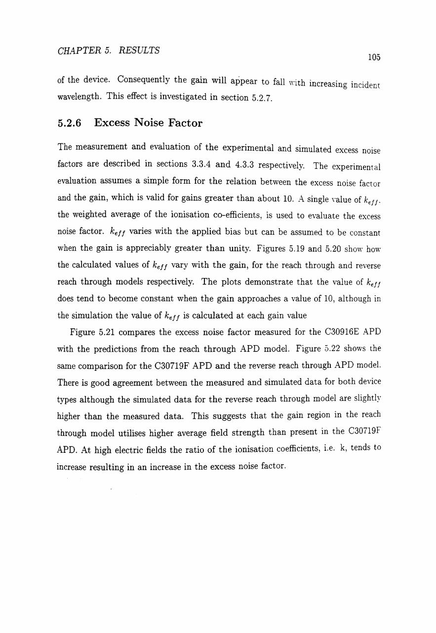
CHAPTER 5. RESULTS 105
of the device. Consequently the gain will appear to fall \,"ith increasing incident
wavelength. This effect is investigated in section 5.2.7.
5.2.6 Excess Noise Factor
The measurement and evaluation of the experimental and simulated excess noise
factors are described in sections 3.3.4 and 4.3.3 respectively. The experimental
evaluation assumes a simple form for the relation between the excess noise factor
and the gain, which is valid for gains greater than about 10. A single ,"alue of kef f.
the weighted average of the ionisation co-efficients, is used to evaluate the excess
noise factor. kef! varies with the applied bias but can be assumed to be constant
when the gain is appreciably greater than unity. Figures 5.19 and 5.20 show how
the calculated values of keff vary with the gain, for the reach through and reverse
reach through models respectively. The plots demonstrate that the value of kef f
does tend to become constant when the gain approaches a value of 10, although in
the simulation the value of kef f is calculated at each gain value
Figure 5.21 compares the excess noise factor measured for the C30916E APD
with the predictions from the reach through APD model. Figure 0.22 shows the
same comparison for the C30719F APD and the reverse reach through APD model.
There is good agreement between the measured and simulated data for both device
types although the simulated data for the reverse reach through model are slightly
higher than the measured data. This suggests that the gain region in the reach
through model utilises higher average field strength than present in the C30719F
APD. At high electric fields the ratio of the ionisation coefficients, i.e. k, tends to
increase resulting in an increase in the excess noise factor.

CHAPTER 5. RESULTS
+
+
+
+
+
+ +
+ + + 1111111111111++++ + ...
, ~
10~~~~~~~--~~~~L-~~~~~~~~~~ 10-' 100 10' 102
Gain
106
Figure 5.19: Plot showing the simulated variation in keff with gam for a reach through model.
10-'
+ + +++++++ + + + + + + + +
++ 10-2 +
+ + + +
10-3 +
+
10-4 +
+ ~i,o~
10'" +
10-7
+
10-8
10-9 10-' 100 10' 102 103
Gain
Figure 5.20: Plot showing the simulated variation in kef f with gain for a rewrse reach through model.

CHAPTER 5. RESULTS
o Measurement + Simulation
10'
/~
o 0+
o-l?
j
1
107
Figure 5.21: Comparison of the excess noise factor measured for a C30916E APD and the predicted excess noise factor from the reach through APD model.
Measurement l Simulation I
+
+
+
+
Figure 5.22: Comparison of the excess noise factor measured for a C30719F APD and the predicted excess noise factor from the reverse reach through model.
The value of keff' hence the excess noise factor, is not solely dependent on
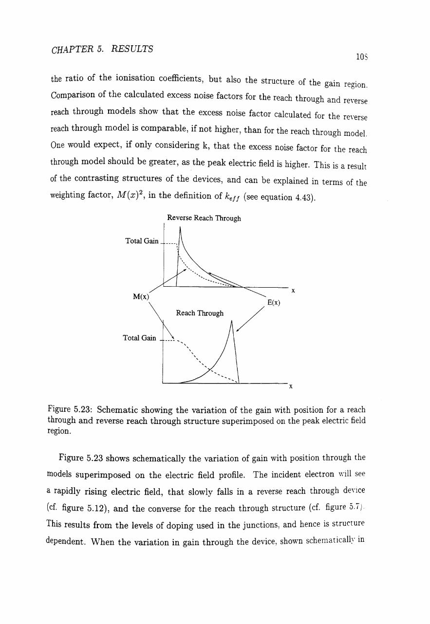
CHAPTER 5. RESULTS lOS
the ratio of the ionisation coefficients, but also the structure of the gain region.
Comparison of the calculated excess noise factors for the reach through and reyerse
reach through models show that the excess noise factor calculated for the reyerse
reach through model is comparable, if not higher, than for the reach through model.
One would expect, if only considering k, that the excess noise factor for the reach
through model should be greater, as the peak electric field is higher. This is a result
of the contrasting structures of the devices, and can be explained in terms of the
weighting factor, M(x)2, in the definition of keff (see equation 4.43).
Total Gain
M(x)
Total Gain
Reverse Reach Through
Reach Through / E(x)
, , , , , , ,
x
x
Figure 5.23: Schematic showing the variation of the gain with position for a reach through and reverse reach through structure superimposed on the peak electric field region.
Figure 5.23 shows schematically the variation of gain with position through the
models superimposed on the electric field profile. The incident electron ,yill see
a rapidly rising electric field, that slowly falls in a reverse reach through deyice
( cf. figure 5.12), and the converse for the reach through structure (cf. figure 5.7)
This results from the levels of doping used in the junctions, and hence is structure
dependent. When the variation in gain through the device, shown schematically in

CHAPTER 5. RESULTS 109
figure 5.23, and the value of keff' which approximates to k2 (see equation -±.-±Ei).
are consisdered then the noise performance of the devices can be explained. In
the reverse reach through device the value of M (x) is highest in the high electric
field region, thus increasing the weighting of the high k values in k Co 1 ef f· nyerse y
for the reach through device, the gradual increase in the electric field results in a
low value of M(x) at the peak field, thus reducing the weighting in that region.
The consequence is that the reverse reach through APD will exhibit a worse noise
performance, compared to the reach through device, for the same peak field, as
suggested by the simulated data.
5.2.7 Photosensitivity
The photosensitivity of a device is defined as the ratio of the photocurrent per watt
of optical power incident on the device. The measurement of the photosensitivity is
described in detail in section 3.3.3. The photosensitivity of the simulated devices is
easily determined from the ratio of the photocurrent and the incident power. The
wavelength and photon flux are parameters in the simulation, hence the incident
power was easily calculated.
Figure 5.24 compares the photosensitivity measured from a C30916E APD with
the calculated photosensitivity from the reach through APD model. The broad
spectral response of the reach through structure results in an almost linear response,
in the measured and simulated data, over the range of wavelengths investigated.
Figure 5.25 shows the same comparison using measurements from the C30179F
APD and data from the reverse reach through APD model. The difference between
the response of the reach through and reverse reach through APD structures is
clearly visible and is replicated by the simulated data. The C30917F APD has a
much narrower response than the C30916E APD. The peak photosensiti"ity is at
600nm, this falls by 25% at 450nm and 800nm.

CHAPTER 5. RESULTS 110
350
0 Measurement
300 + Simulation 0
0
250 0
-~ !!: 200 0
~ :~ .~ c: 0 ., B 150 0 .c c.. 0 +
+ +
100 0 + +
+ 0 +
50 +
0 400 450 500 550 600 650 700 750 800 850
Wavelength Inm
Figure 5.24: Comparison of the photosensitivity measured for a C30916E APD and the predicted photosensitivity from the reach through model at 300V.
25r---~----.----.-----r----r----r----r----r--~
20
I I
I
I I
I
o
/ /
/
/ /
/
o
/
o
o
, , , ,
1- ~-
o
, , , , , 0 , , , ,
Measunnent l Simulation
, , , , 0
1~OLO----~~0----~500-----55~0----~~0----65~0--~7~00--~7~50~~8=OO~~850 Wavelength Inm
Figure 5.25: Comparison of the photosensitivity measured for a C30719F APD and the predicted photosensitivity from the reverse reach through model at 300V.

CHAPTER 5. RESULTS 111
The photosensitivity is affected by variation in the gain. Figure 5.26 shows the
gain measured for the C30916E APD and predicted by the reach through APD
model. Both the measurements and the predictions remain un-affected by variation
in the incident wavelength. Figure 5.27 shows the same plot for the C30719F APD
and the reverse reach through model. Now the gain falls dramatically as the incident
wavelength increases, this effect has been measured in similar devices [96]. The fall is
due to incident light being absorbed in, or even beyond the gain region, as described
in section 5.2.5. The fall in the measured gain is essentially a mis-calculation of
the gain. The multiplying power of the gain region is not affected by the change in
incident wavelength, there is simply less of the initial photo-generated charge being
multiplied.
103 .------..,------,-----;----,------,------:
o 450nm x 650nm + 750nm
450nm 650nm 750nm
10-' L--~----L...---:-::-------:200;;;;--~2;;.50:;---~300 o 50 100 150 BiasN
Figure 5.26: Plot showing the variation in gain with incident wavelength meas~red for a C30916E APD and predicted by the reach through model. The data pomts show the measurements and the lines show the model's predictions.

CHAPTER 5. RESULTS 112
103 r--r----,-----r----r---;---""T""-__
0 450nm X 650nm + 750nm
450nm
102 660nm
790nm
10-1~-____::_-~~----I.----.L-----L.....--...l...------l o 50 100 150 200 250 300 350
BiasN
Figure 5.27: Plot showing the variation in gain with incident wavelength measured for a C30719F APD and predicted by the reverse reach through model. The data points show the measurements and the lines show the model's predictions.
5.3 Post-Irradiation
The devices were irradiated at the Rutherford Appleton Laboratory's ISIS facility
(see section 3.3.6). To allow useful comparison between the dose received at different
neutron irradiation facilities, it is common to express the flux in terms of l::-vle\"
neutrons. This is achieved by multiplying the integrated flux over a specific energy
range e.g. > lOKeY, by the hardness parameter. The hardness parameters are
available for most facilities, for the ISIS facility the hardness parameter is 1.02
[97],[98]. Thus the integrated flux provided by ISIS can immediately be converted
into the lMe V equivalent. The following results report all the neutron fiuences in
terms of the lMe V equivalent.
5.3.1 Reach Through APD
The effect of neutron irradiation on the internal structure of the reach through
APD can be investigated using the simulation. At 50V the increase in the thermal
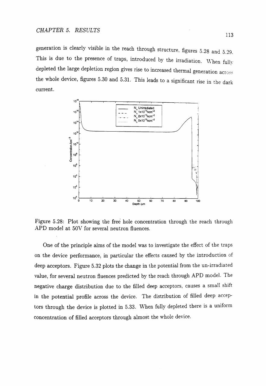
CHAPTER 5. RESULTS 113
generation is clearly visible in the reach through structure fig - 28 _ ~ ures Ll. and Ll.29.
This is due to the presence of traps, introduced by the irradiation. \\-hen fully
depleted the large depletion region gives rise to increased thermal . generatIOn across
the whole device, figures 5.30 and 5.31. This leads to a significant rise in the dark
current.
Nh Unirradiated Nh 1X10'3ncm-2
Nh 2x10'3ncm-2
Nh 5x10'3ncm-2
10° '---"--_'------J_---l._---L_--L._--L..._----1-._--I-_
o 10 20 30 40 50 60 70 80 90 100 Depth/11m
Figure 5.28: Plot showing the free hole concentration through the reach through APD model at 50V for several neutron fiuences.
One of the principle aims of the model was to investigate the effect of the traps
on the device performance, in particular the effects caused by the introduction of
deep acceptors. Figure 5.32 plots the change in the potential from the un-irradiated
value, for several neutron fiuences predicted by the reach through APD model. The
negative charge distribution due to the filled deep acceptors, causes a small shift
in the potential profile across the device. The distribution of filled deep accep
tors through the device is plotted in 5.33. When fully depleted there is a uniform
concentration of filled acceptors through almost the whole device.

CHAPTER 5. RESULTS
N e Uninadiated N 1x10'3ncm-2
N& 2x10'3ncm-2
Ne
5X10'3ncm-2 e
;;--. __ . __ . __ . __ ._. __ . __ . __ ._-...... " I \
106 ' \ \ .. \ /
~r I
102 .:-.---:-:----::---=----::--=---::----:L-----1..----l--o 10 20 30 40 50 60 70 80 90 100
Depth/llm
114
Figure 5.29: Plot showing the free electron concentration through the reach through APD model at 50V for several neutron fiuences.
"Ie ..................... ···································································0 ~ 10'0 - -- _. __ ._. __ ._. __ .- -_.- -- -.--.- --.- -- -.- -------
§ - - - - - - - - - - - - - - - - - - - - - - - - - - - - - ---------f '! ~ 108 (.)
8
100 L-..l----'----L-----..lI.--=----::---=-----:;:--~90;:;-~100 o 10 20 30 40 50 60 70 80 Depth/llm
Figure 5.30: Plot showing the free hole concentration through the reach through model at 300V for several neutron fiuences.
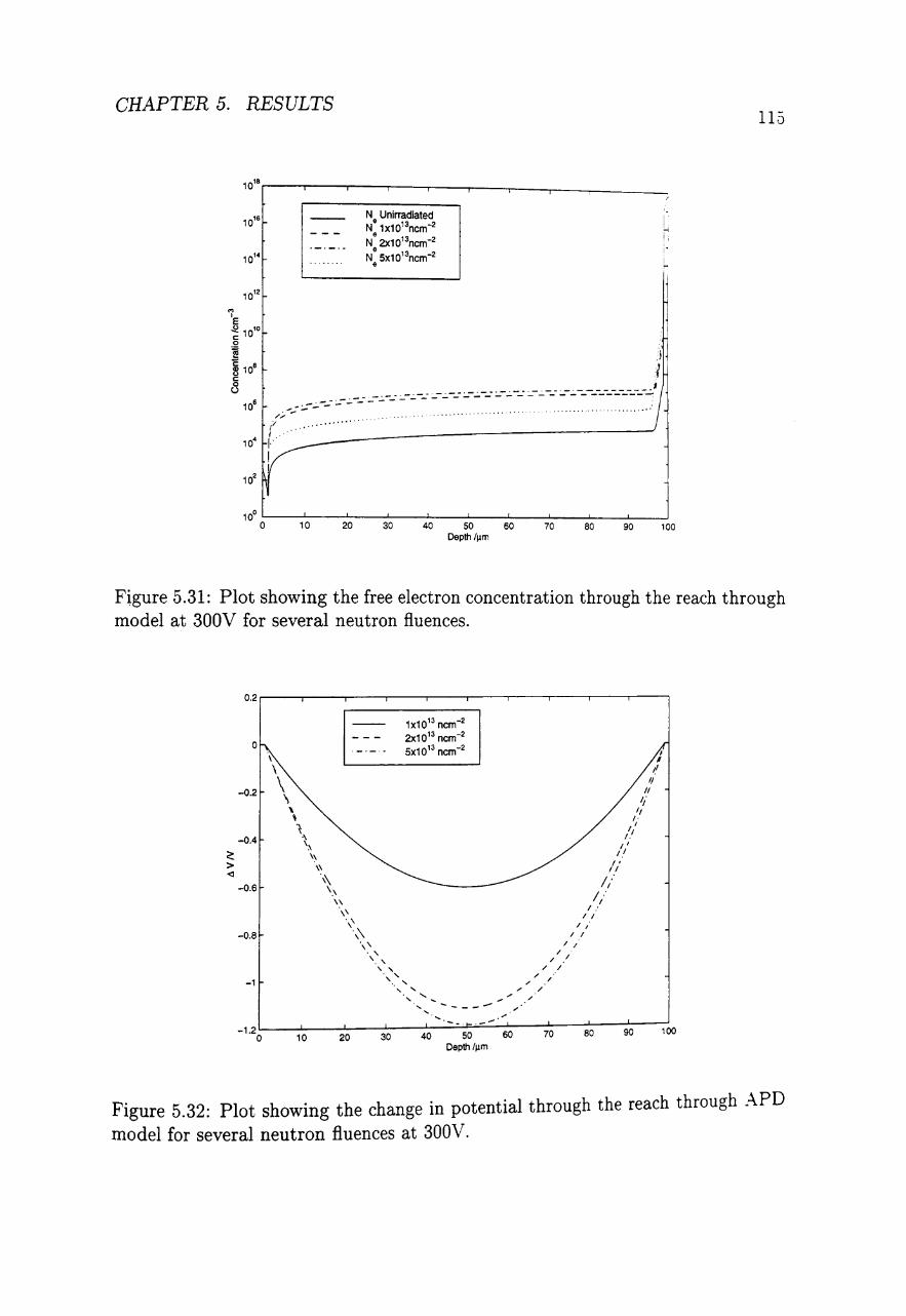
CHAPTER 5. RESULTS
10'8r -.----r------r--r---.---.-_--._--, ___ _
N Unirradiated N
e 1x10'3ncm-2
Ne
2x10'3ncm-2
Ne
5X10'3ncm-2 e
- . - -_. -_. ---:..:-~ --- ~-- --- ~-~ ------------.. :.::...-~.' - _. '--,.;.. --- - - -...-,..::.:.:----:.;.---- --
1~~-~-~-~~~~-~-~-~-~-~-~ o 10 20 30 40 50 60 70 80 90 100 Depth fJ.lm
11.5
Figure 5.31: Plot showing the free electron concentration through the reach through model at 300V for several neutron fluences.
0.2,---.-----.---,--.----.---.....,-----,----,,--.----,
o , \
-0.2 \ \ ,
l .~
1x10'3 ncm-2
2x10'3 ncm-2
5x10,3 ncm-2
" ,.
I I
~I 1/
/I ,,-
-0.4
~
., \ \~
" ,l
" ,l
> <I "
-0.6 \\ '.,
" -0.8
-1
, ' /I
1/ 1/ , :
I ,
I " I I
1/ I
/ ./ / I
/ .. / ./
" /
-1.20L-~10--2...L.0-~30--4.l-0~-:...:.-""!:~0~~6=-0--::70~---;;8;-0 -~90~~100 Depth fJ.lm
Figure 5.32: Plot showing the change in potential through the reach through APD model for several neutron fluences at 300V.

CHAPTER 5. RESULTS
10" r----,c-----,---,------,.----,--r----,r----,_-,_---.
1012 r-~ --- --~ ---:.-~ ---:.-~ ---:.-.:.. --- :.-~ ---:.-~ ---:.-~ ---:.-~ -_-:.-:. __ -_-_-___ -_-_-_-. ~~
10"
1x10¹³ ncm-2
2X10¹³ ncm-2
5x10¹³ ncm-2
1 ~ i
1
1 04 ~---:-:____::--____=:____7::_____::______::L..---L..-------1.---.J o 10 20 30 40 50 60 70 80 90 100
Depth/j.lm
116
Figure 5.33: Plot showing the distribution of filled acceptors through the reach through model for several neutron fluences.
To describe qualitatively the macroscopic effects due to the introduction of the
filled deep acceptor levels, the distribution of the filled traps should be considered.
Figure 5.33 shows that the majority of the deep acceptors occur on the p side of the
junction region. Thus the large build up of negative charge increases the potential
drop across the reverse biased junction. This will have the effect of increasing the
electric field in the gain region.
5.34 shows the simulated effect of the introduction of filled deep acceptors on
the multiplication factor of the reach through APD. The multiplication factor of the
device is predicted to increase after irradiation with neutrons. This effect has not
been experimentally verified. There are several reasons for the lack of experimental
verification.

CHAPTER 5. RESULTS
103r--:==::::==~= .......... -"""-----;-__ --' __ ---, __ _
l Unirradiated l 2X10'3ncm-2
10'
o x
® ®
o
x
o x o
1000~"""""""""'~"'~®:::"-----::::::-----:-::----::-:----.l....------L--~ 50 100 150 200 250 300 350
BiasN
117
Figure 5.34: Plot showing the multiplication factor III the reach through model before and after neutron irradiation.
103r----.----.----,------r----~--~
10'
I I
I I
I
x x x x x x x x ~ x X I
j '" -- '"
I
'" "
I I
I x
I
o
o x
x x
Measurement (Unirrad) Measurement (1.6+I-O.3x1 O'3ncm-2)
Simulation (Unirrad) Simulation (2x10 '3ncm-2
)
10~L-----~----~------L------.l....------~----~ o 50 100 150 200 250 300
BiasN
Figure 5.35: Plot showing the measured photo current in a C30916E APD and predicted by the reach through APD model before and after neutron irradiation.

CHAPTER 5. RESULTS 11S
Firstly, as figure 5.17 demonstrates, the exact evaluation of the multO l' . Ip lcatlOn
factor is not a trivial process. This is particularly relevant in the case of the C30916E
APD. Figure 5.35 shows the C30916E photo current measured before and after neu
tron irradiation. The photocurrent predicted by the reach through APD model is
also shown. Both the predictions and the measurements show a severe degradation
in the detection of light at low bias. This can be attributed to the increased recom
bination due to the traps introduced by the neutron radiation; a similar effect is
observed in irradiated solar cells [99].
The model predicts this behaviour well, but does not explain the overall fall in
the measured photocurrent or the flatter profile that occurs at higher bias. The
discrepancies can be explained as follows. The uniform fall in the measured pho
to current can be attributed to surface damage in the device from the gamma back
ground present during the irradiation. Surface effects are not included in the model,
and hence cannot be re-produced. The C30916E APD is housed in a hermetically
sealed TO package where the actual device is in limited contact with the case. Af
ter neutron irradiation and at high reverse bias, the total current can exceed lILA.
Controlling self-heating in the device becomes difficult under these conditions. An
increase in APD temperature will reduce the ionisation coefficients and hence the
gain, even though the electric field may have increased in the gain region. Accurate
evaluation of the gain, from the photo current measurements, is not possible because
of the reduced charge collection at low bias. The un-multiplied photocurrent cannot
be determined.
The measured change in the photosensitivity for the C30619E is dominated by
the surface damage from the "'( background present during the irradiation [100]. At
300V the fall is significant, figure 5.36. The model which excludes surface effects.
due to its one dimensional nature cannot predict these effects. Although the model
predicts the change in response at low bias, at high bias surface damage and self
heating become dominant in the C30916E performance.

CHAPTER 5. RESULTS 119
350
0 Measurement (Unirrad) x Measurement (1.6+I-O.3x1 013ncm- 2)
300 Simulation (Unirrad) 0
Simulation (2x1 013ncm-2) 0
250 0
-;: ~ 200 0 >-... ~ 'iii c:: 0 CIl
£ 150 0 .c
Q. 0
100 9,- -50
x x x x
x x 0 400 450 500 550 600 650 700 750 800 850
Wavelength Inm
Figure 5.36: Plot showing the measured photosensitivity in a C30916E APD and predicted by the reach through model before and after neutron irradiation.
5.3.2 Reverse Reach Through APD
Figures 5.37 and 5.38 show the affect of neutron irradiation on the free hole and
electron concentration in the reverse reach through APD model at 50\ ~. As with
the reach through APD a large increase in the thermal generation is visible in the
depleted region at the front of the device. At 300V, figures 5.39 and 5.40, there is a
uniform increase in the thermal generation across the majority of the device, which
is almost completely depleted.

CHAPTER 5. RESULTS
10'81-----.-----r----.-----_r--__ ---. ___ ~
Nh Unirradiated Nh 1x10'3ncm-2
Nh 2X10'3ncm-2
Nh 5X10'3ncm-2
1if~--~---~---~--~~--~---~ o ~ ~ ~ 80 100 120 Depth/11m
120
Figure 5.37: Plot showing the free hole concentration through the reverse reach through model at 50V for several neutron fluences.
10'8 ,.-__ ---,-___ --r-___ -r---__ ---, ___ ---,-___ -,
20 ~
N Unirradiated N
e 1x10'3ncm-2
Ne
2x10'3ncm-2
Ne
5x10'3ncm-2 e
60 Depth /Ilm
80
II . ---.. // .. ,
100 120
Figure 5.38: Plot showing the free electron concentration through the reyerse reach through model at 50V for several neutron fiuences.

CHAPTER 5. RESULTS
10'81---.,-----r----.-___ ~--~---
Nh Unirradiated Nh 1X10¹³ncm-2
Nh 2x10¹³ncm-2
Nh 5x10¹³ncm-2
~~" ," ................. . \~~:..:.:: .:---:..-- --- :..-.:.. --- ------- :..-.:.. --~',------ ,--~ -- -' ~----- -.- ..... - - - --~~ ........ "
,,', '\
1~:----~~----~------~----~--~-----~ o 20 40 60 80 100 120 Depth/!lm
L~l
Figure 5.39: Plot showing the free hole concentration through the reverse reach through model at 300V for several neutron fiuences.
10'8,------.,-----r-------r------,.-----.------,
N Unirradiated N° 1X10¹³ncm-2
Ne
2x10¹³ncm-2
Ne
5x10¹³ncm-2
°
... -........................................... ' ........ .
:;:-~::.-::..::..:..:.----~ --- ----~ --- ----~ --- ----~ --- ----~ --- ----~ --- ----.:. --- ~.:. --- ---~ --- ---.:.-.,:
i
6 1 __ -------------------------1 10 v/ 10· ,
!
1~L-----~----~------~----~----~100~---~120 o 20 40 60 80 Depth /!lm
Figure 5.40: Plot showing the free electron concentration through the reverse reach through model at 300V for several neutron fiuences.

CHAPTER 5. RESULTS 1:2:2
Figure 5.41 shows the predicted shift in the potential through the reverse reach
through APD. The plot is very similar to figure 5.32 but the magnitude of the shift
is much greater for the reverse reach though APD. When the potential through the
reverse reach through APD is plotted for several neutron fiuences, figure .:5 . .,12. the
shift is clearly visible. The similarity can be understood by comparing figures 5.-l3
and 5.33. The uniform distribution of filled acceptors through the reverse reach
through APD, figure 5.43, is similar to that in the reach through APD.
1x10'3ncm-2
2x10'3ncm-2
" 5x10'3ncm-2
\', , , , I -1 "-
"- .... /'" I
,.- I
I
-2 --- ------ I
I ~ I > I <l
I -3 ,
/ , / ,
/ , / ,
/ -4 , / ,
/ , "- /'
" -5 ;
-6 0 20 40 60 80 100 120
Depth/11m
Figure 5.41: Plot showing the change in potential across the reverse reach through model for several neutron fiuences at 300V.

CHAPTER 5. RESULTS
c:: 1i!
350~----~-------r--____ ,-____ ~ ______ ~ ____ __
300
250 . ~ ....... ' .
200
'E 150
~ 100
Unirradiated 1 xl 0 '3ncm-2
2xl0'3ncm-2
5x10'3ncm-2
-50~----~~----~~-----L------~ ______ ~ ____ ~ o 20 40 60 80 100 120
Depth/11m
Figure 5.42: Plot showing the potential across the reverse reach through model at 300V before and after neutron irradiation.
1 0'4 ~------'---------'--------'--------'------__ r------.....,
10'2 ~-_-___ -_-_-___ -__ ~~-~ -_- ~-~ -_- ~-~ -_- ~-~ -_- ~-~ -~ ~-~ -_- _-_ -_- _-_ -_- ~-~ -_- _-_ -~
lx10'3ncm-2 2X10'3ncm-2 5x10'3ncm-2
1oSoL-----~2~0------~40------~6~0------~80~----~loo~----~'20 Depth/Ilm
Figure 5.43: Plot showing the distribution of filled acceptors through the re\-erse reach through model for several neutron fiuences.

CHAPTER 5. RESULTS 12--1
The multiplication factor predicted by the reach through APD model. figure
5.34, showed an increase after neutron irradiation. The change in the multiplication
factor with neutron fiuence, predicted by the reverse reach through model~ is shown
in figure 5.44. In contrast to the reach through APD model the multiplication
factor reduces after neutron irradiation. This is also due to the presence of negatiye
space charge caused by the filled deep acceptors. The design of the reverse reach
through APD results in the majority of the space charge forming on the n side of the
junction. This has the opposite effect to that observed in the reach through model.
The potential difference across the gain region is reduced, resulting in a drop in the
electric field and the gain.
I ~ Unirradiated I 2x10¹³ncm-2 J
o x
oQQ o x x
o o x
o x o x
o x 9 x
o
x o
x
Figure 5.44: Plot showing the multiplication factor predicted by the reverse reach through model before and after neutron irradiation.
Figure 5.45 shows the measured photo current for a C30719F~ before and after
neutron irradiation. The photocurrent predicted by the reverse reach through APD
model is also shown. Unlike the C30619E, the C30719F does not show any significant
degradation in the low bias charge collection. This is due to the position of the gain
region, whereby the majority of the signal charge is still generated in the depleted

CHAPTER 5. RESULTS
reglon. There is a uniform fall in the measured photo current n t d' d , 0 pre lete by the
model, again this is attributed to surface damage introduced d' h' " urmg t e IrradIatIOn.
10' rr=========:::::J====::=r:=====::c==::::---,----.,.-----, o l(
10' 00000
50
Measurement (Unirrad) Measurement (1.6+/-O.3x10 '3ncm-2) Simulation (Unirrad) Simulation (2x10'3ncm-2)
/
x
l(
100 150 200 BiasN
x x
x x
250 300 350
Figure 5.45: Plot showing the measured photo current in a C30719F APD and predicted by the reverse reach through model before and after neutron irradiation.
Figure 5.46 compares the gain measured for the C30719F with the gain predicted
by the reverse reach through APD model, both before and after neutron irradiation.
The predicted gain has been shifted along the x-axis to aid the comparison. The
experimental results show a fall in the gain, that is replicated well by the model. It
can be considered that after neutron irradiation the gain curve is actually shifted
along the bias axis. This idea was suggested by Y. Musienko et aI, when presenting
results after the irradiation of C30626E reverse reach through APDs [15]. The effect
only becomes significant when the device is depleted and the re-arrangement of free
carriers cannot cancel the effect of the filled acceptors. The shift in the gain is
seen to occur, both experimentally and from the model's predictions, just before the
device 'reaches through'. At very high reverse bias the role of self-heating may play
a small part in the reduction of the gain, although the packaging of the C30i19F in
fiatpacks allowed much better temperature control.

CHAPTER 5. RESULTS 126
The photosensitivity of the C30719F measured before and after neutron irradi
ation is shown in figure 5.47. The predictions from the reverse reach through APD
model are also shown. The model predicts that the reduced photosensitivity is com
pletely described by the fall in gain. The measured fall in the photosensitivity is also
affected by surface damage, which is not included in the model. Thus the measured
fall in the photosensitivity is not completely predicted by the model.

CHAPTER 5. RESULTS
103r-----,------.------.-----~------r_------____ _
o
* Measurement (Unirrad) Measurement (1.6+/-0.3x1 0' 3ncm-2) Simulation (Unirrad) Simulation (2X10'3ncm-2)
/
10-' :------:':------I. ______ -'--____ --L. ____ ----''--____ -'--____ ---l o 50 100 150 200 250 300 350
BiasN
1,,-_I
Figure 5.46: Plot showing the change in the measured gain for the C30719F APD and predicted by the reverse reach through model before and after neutron irradiation.
25
0 0
0
20 0
0
-~ 15
~ ::;e 0 :~
/ c: / (I)
'" / 0 / ,g 10 x x 0- x
x x
x
x x
5 0 Measurement (Unirrad) x Measurement (1.6+/-0.3x1 O'3ncm-2)
Simulation (Unirrad) Simulation (2x10'3ncm-2)
0 550 600 650 700 750 800 850
400 450 500 Wavelength Inm
Figure 5.47: Plot showing the change in the photosensitivity measured for a C30719F APD and predicted by the reverse reach through model.

Chapter 6
Conclusions
A one-dimensional drift-diffusion simulation has been developed incorporating im
pact ionisation, illumination and neutron radiation damage effects. Impact ionisa
tion is included via a term in the continuity equations. The ionisation coefficients
in silicon are described using a modified form of the three parameter theory. This
method has been successfully used to simulate temperature dependent effects in
silicon avalanche photodiodes [93]. Illumination is accounted for using a param
eterisation of the absorption coefficients in silicon, measured by Dash et al [85].
The effects of neutron irradiation damage are included via the introduction of deep
acceptor levels. The occupancy of the defects is described by Shockley-Read-Hall
statistics; quasi-Fermi statistics were found to cause severe convergence problems.
The simulation software was used to generate two complementary silicon avalanche
photo diode models; a reach through structure and a reverse reach through structure.
The predictions from the models were compared with measurements performed on
two commercial silicon avalanche photodiodes; the EG&G C30916E reach through
APD and the EG&G C30719F reverse reach through APD. The structures of the
commercial devices were not known in detail, this proved a major hurdle~ allowing
only qualitative comparison with the predicted data.
The simulation allows investigation of the microscopic structure of the devices
during operation, as well as providing macroscopic information. Good agreement
was found between the predicted and measured behaviour under re\'erse bias for both
128

CHAPTER 6. CONCLUSIONS 129
models. The 'reach through' process was described by the models' both . ~ mIcroscop-
ically, by the distribution of free carriers, and macroscopically from the predicted
photo current .
Complementary methods were used to calculate the gain from the models. di
rectly from the predicted photo current and indirectly from analysis of the electric
field profile. This allowed the models to predict the gain that would be measured
experimentally and to compare this with the multiplication factor of the deyices. i.e.
the actual gain experienced by a charge traversing the gain region. The use of the.
DC gain measurement was shown to overestimate the gain for reach through struc
tures, as light is absorbed in an un-depleted region prior to 'reach-through'. The fall
in gain at longer wavelengths, for the reverse reach through structure, was predicted
by the model. This effect is caused by the absorption of light in, or beyond, the gain
region. Only the electrons generated in front of the gain region are fully multiplied.
This results in a fall in the measured gain, although the multiplication factor of the
device is un-affected.
The excess noise factor was calculated from the models using the Mcintyre theory:
measurements of the excess noise factor were achieved using the Webb method. The
predicted excess noise factor compared well with the measured data, although no
post-irradiation comparison was available.
The photosensitivity was calculated from the models and compared with the
measured data. The reach through structure exhibits a broad spectral response.
due to the wide depletion region available for the absorption of the incident light.
The smaller region available in the reverse reach through structure results in a much
narrower response. The simulation predicted the measured response well, for both
structures.
The effects of neutron irradiation were investigated. To facilitate comparison
with experimental data the C30916E and C30719F devices were irradiated at the
RAL ISIS facility. The reach through APD model predicted an increase in the mul
tiplication factor after neutron irradiation. This was not confirmed experimentally

CHAPTER 6. CONCLUSIONS 130
because the method used to measure the gain could not be successfully applied to
the C30916E device after irradiation. The measured photo current data implied a
reduction in the gain after irradiation for the C30916E device. This was attributed
to self-heating in the C30916E device due to the increased bulk dark current and
limitations in the temperature control imposed by the C30916E packaging.
The gain of the reverse reach through model was seen to fall after neutron irra
diation. The gain measured from the C30917E device showed a similar reduction.
This effect has also been observed in measurements of EG&G C30626E reverse reach
through avalanche photodiodes during evaluation for the CMS ECAL .
The observed shift in the gain is attributed to the presence of ionised deep
acceptor levels, which alter the potential through the device; this in turn modifies
the electric field profile. The gain is extremely sensitive to changes in the electric
field and a small shift in the high field region, where the gain originates, will result
in a significant change in the gain.
The measured photosensitivity of the C30916E and C30719F devices fell signifi
cantly after neutron irradiation. This trend was reproduced by the models, but the
fall was not described completely. The gamma background during the irradiations
introduced surface damage to the devices, resulting in a fall in the quantum effi
ciency and hence photosensitivity. Surface damage was not included in the model
and hence the effects could not be completely described.
A general-purpose simulation tool has been introduced, which allows complex
photodiodes to be built and tested, both before and after neutron irradiation [101],[102:.
Two complementary silicon avalanche photo diode models have been compared '''lith
measured data from commercial devices with similar structures. The models shmved
good qualitative agreement with the measured data for a wide range of conditions.
and indicated areas where further development would be beneficial. The results
show that the simulation software is a useful tool in the analysis of silicon photode
tectors, and could be applied to the development of future devices: especially in
HEP where radiation tolerant devices are essential.

CHAPTER 6. CONCLUSIONS 131
The simulation package provides an excellent platform for further deyelopment.
The two primary areas of interest for expansion are, simulation of multiple spatial
dimensions and the solution of the time-dependent equations. Simulation of t\\·o
or three-dimensional structures would allow much more complete modelling of de
vice behaviour including surface effects and lateral non-uniformities, which lead to
micro-plasma formation. The solution of the time-dependent equations would allow
the investigation of transient effects, e.g. the formation of avalanches as a result
of particle interaction. These developments are not mutually exclusive, a multi
dimensional time-dependent simulation would be an extremely versatile tool in the
analysis of avalanche photo diode behaviour.

Bibliography
[1] J Gower," Optical Communication Systems" ~ Prentice Hall, 1993, CK
[2] S L Miller," Avalanche Breakdown in Germanium", Phys. Rev, Vol. 99, 1955,
pp 1234-1241.
[3] T shima and Y Nagai," Development of a Photomultiplier Tube with high
Quantum Efficiency. ", Nucl. Instr. and Meth., A 431,no.I-2, 11 July (1999).
pp. 224-227.
[4] J A Correia et al ,"Development of a Small Animal PET Imaging Device with
Resolution Approaching 1 mm." , IEEE Transactions on Nuclear Science, Vol.
46, no. 3, pt. 2, Jun 1999, pp. 631-635.
[5] Suzuki A et al," Improvement of 20 in. Diameter Photomultiplier Tubes. ",
Nucl. Instr: and Meth., A 329,no.1-2, 15 May (1993), pp. 299-313.
[6] K D Kramer et aI," An Optical MEMS-Based Fluorescence Detection Scheme
with Applications to Capillary Electrophoresis." ,Proceedings of SPIE, vol.
3515, 1998, pp.76-85. USA.
[7] R Farrell et aI," Advances in Semiconductor Photo detectors for Scintillators.
", Nucl. Instr. and Meth., A 387, (1997), pp. 194-198.
[8] K M James et al," Performance Evaluation of Ne"w Large-Area Asalanche
Photo diodes for Scintillation Spectroscopy. ", Nucl. Instr. And AIeth." A 313.
(1992), pp. 196-202.
132

BIBLIOGRAPHY 133
[9] S M Sze," Physics of Semiconductor Devices", John \Viley & Sons. eSA.
1981.
[10] J Zhang et al ," Military Avionics Optical Fiber Data Buses 'with Actiye
Coupler Configurations.", IEEE Aerospace and Electronic Systems lUagazine
,Vol. 14, no. 7, July 1999, pp. 27-33.
[11] Proceedings of SPIE, vol. 3000, 1997, pp.55-59. USA.
[12] R Lecomte et al ,"Performance Characteristics of BGO-Silicon Avalanche Pho
todiode Detectors for PET.", IEEE Transactions on Nuclear Science,Vol. NS-
32, no. 1, Feb 1985, pp. 482-6.
[13] P Cushman et al," Multi-Pixel Hybrid Photodiode Tubes for the CMS Hadron
Calorimeter. ", Nucl. Instr. and Meth., A 387,no.I-2, 1 Mar, (1997), pp. 107-
112.
[14] G Organtini ," Avalanche Photodiodes for the CMS Electromagnetic Calorime
ter. ", IEEE Transactions on Nuclear Science,Vol. 46, no. 3, pt. 1, Jun 1999,
pp. 243-9.
[15] The CMS Collaboration, " The Electromagnetic Calorimeter Project Technical
Design Report", CERN/LHCC 97-33(1997).
[16] The CMS collaboration, " The Compact Muon Solenoid letter of Inten(',
CERN/LHC 92-3 LHCC/I1(1992)
[17] The CMS collaboration, " The Compact Muon Solenoid Technical Proposal".
CERN/LHC LHCC/9438(1994). -
[18] J P Ernenwein, " Overview of the CMS Electromagnetic Calorimeter ". C:\IS
CR/99/006.
[19] K Dieters et al," Comparison of Photomultiplier and Avalanche Photodiode
Readout of PbW04• ", Nucl. Instr. and Meth. , A 387. (1997), pp. 211-213.

BIBLIOGRAPHY 13-1
[20] R J McIntyre, P P Webb and H Dautet," A Short \\"avelength Selectiye
Reach Through Avalanche Photodiode", IEEE Transactions on Xuclear Sci
ence, Vol. 43, June 1996, No 3, pp. 1341-1346.
[21] E Longo," Avalanche Photodiodes for the eMS Electromagnetic Calorimeter~' .
CMS CR1998/002, 1998.
[22] J P Pansart," Avalanche Photodiodes for Particle Detection" , Nucl. Instr. and
Meth., A 387 (1997), pp. 186-193.
[23] J Matheson, M Robbins and S J Watts," A Microscopic Explanation for Type
Inversion and the Annealing Behaviour of Radiation Damaged Silicon Detec
tors", BRU /PH/202, 19 May 1995.
[24] J Matheson et aI," The Effect of Radiation Induced Defects on the Performance
of High Resistivity Silicon Diodes", RD20/TN/36, Jan 1995.
[25] D Pusseri et aI," Comprehensive modelling of Silicon Microstrip Detectors",
CMS CR/97/004, 1997.
[26] For example see M J Morant," Introduction to Semiconductor Devices", Har
rap, 1970
[27] W Shockley," The Theory of p-n Junctions in Semiconductors and p-n Junc
tion Transistors", Bell Systems Tech. Jour. 28, 1949, p-435
[28] R N Hall, Phys. Rev, Vol. 87, 1952, p-387.
[29] W Shockley and W TRead, Phys. Rev, Vol. 87, 1952, p-835.
[30] A G Chenowyth, Phys. Rev, Vol. 109, 1958, p-1537.
[31] S M Sze and G Gibbons," Avalanche Breakdown Voltages of Abrupt and
Linearly Graded p-n'Junctions", Applied Physics Letters, Vol. 8. \'0. 5. 1966.
p-l11.

BIBLIOGRAPHY 13·)
[32] J Conradi," The Distribution of Gains in uniformly :\Iultiplying Avalanche
Photodiodes ", IEEE Transactions on Electron Devices, Vol. 19,Jul 1972,
No, 6, pp. 713-718.
[33] P P Webb, R J McIntyre and J Conradi, " Properties of Avalanche Photodi
odes", RCA Review, Vol. 35, June 1974, p-234.
[34] R J McIntyre" Multiplication Noise in uniform Avalanche Photo diodes ".
IEEE Transactions on Electron Devices, Vol. 13,Jan 1966, :'\0. 1, p-16-!.
[35] K Roze et aI," Temperature Dependence of Impact Ionisation Co-efficients in
P-Si ", Journal of Applied Physics, Vol. 83, no. 9, May 1998, p-4988.
[36] A Pacelli et aI," Impact Ionisation in Silicon: A Microscopic View ~', Journal
of Applied Physics, Vol. 83, no. 9, May 1998, p-4760.
[37] J Y Tang and K Hess" Impact Ionisation of Electrons in Silicon(Steady State)
", Journal of Applied Physics, Vol. 54, no. 9, Sep 1983, p-5139.
[38] a good list is provided by W Meas, K DE Meyer and R Vanoverstraeten, ,.
Impact Ionisation in Silicon: A Review and Update", Solid State Electron
ics,Vol. 33, No.6, 1990, pp 705-718.
[39] P Bhattacharya," Semiconductor Optoelectronic Devices", Prentice Hall In
ternational Editions, USA, 1994
[40] J E Bateman and R Stephenson," Charge Storage Effects in Some Avalanche
Photodiodes Proposed for use in the CMS ECAL", RAL-TR-95-061, 1995
[41] N Bacchetta et aI," MRS Detectors with High Gain for Registration of \\-eak
Visible and UV Fluxes", Nucl. Instr. and Meth.: A 387, 1997, pp. 22.:)-230.
[42] A V Akindinov ," New Results on MRS APDs", Nucl. Instr. and jUeth .. A
387, 1997, pp. 231-234.

BIBLIOGRAPHY 136
[43] EG&G Inc. 43 William Street, Wellesley, Maassachusetts. (SA.
www.eg+g.com .
[44] Y Benhammou ," Investigation of Avalanche Photodiodes" ~ C~IS T\/96/0.J2~
1996.
[45] F Cavallari ," Progress on avalanche Photodiodes as Photon Detectors for
PBW04 Crystals in the CMS Experiment", CMS CR/97/10, 1997
[46] E Bartolome et aI, "Development of a Compact high Density Luminosity ~Ion
itor for ALEPH at LEP-II based on a Tungsten-Scintillator Calorimeter read
out by Avalanche Photodiodes" ,Nucl. Instr. and Meth., A 387, 1997, pp. 216-
219.
[47] J Troska, "Neutron, Proton and I' Radiation Effects in Candidate InGaAs
Photo diodes for the CMS Tracker Optical Link", CMS TN /97/102, 1997
[48] Th. Kirn et al , " Properties of the Most Recent Hamamatsu Avalanche Pho
todiodes", Nucl. Instr. and Meth., A 387, 1997, pp. 199-201.
[49] B MacEvoy et aI," Defect Evolution in Silicon Detector Material" ,Nucl. Instr.
and Meth., A 388, 1997, pp. 365-369.
[50] R Wunstorf et aI, "Radiation Damage of Silicon Detectors by Mono-Energetic
Neutrons and Electrons" , Large Hadron Collider Workshop, v.3, Aachen, Ger
many, 4-9 October, 1990. (CERN 90/10 p.706)
[51] S J Watts, " Overview of Radiation Damage in Silicon Detectors - \Iodels and
Defect Engineering" ,Nucl. Instr. and Meth., A 386, 1997, pp. 149-155.
[52] F M Lemeilleur et aI," Electrical Properties and Charge Collection Effi
ciency for Neutron-Irradiated p-type and n-type Si Detectors". Nucl. Instr.
and Meth., B 387, (1993), pp. 415-424.

BIBLIOGRAPHY 137
[53] R Wunstorf et aI, " Results on Radiation Hardness of Silicon Detectors up
to Neutron Fluences of 1015n/cm2" ,Nucl. Instr. and Meth., A 315~ 1992, pp.
149-155.
[54] K Gill, G Hall and B MacEvoy," Divacancy Clustering and the Origin of
Leakage Current in Bulk Damaged Silicon Detectors", CMS/TN/96/17~ 1996.
[55] K Gill, G Hall and B MacEvoy," Bulk Damage Effects in Irradiated Silicon
Detectors Due to Clustered Divacancies", CERN-PPE/97/11, Feb 1997.
[56] M Moll et aI," Comparison of Defects Produced by Fast Neutrons and 60Co_
gammas in High Resistivity Silicon Detectors using Deep Level Transient Spec
troscopy" , HH/96/01, 1996
[57] S J Watts et aI," A New Model for Generation-Recombination in Silicon De
pletion Regions after Neutron Irradiation", IEEE Transactions on Nuclear
Science, Vol. 43,No. 6, Dec 1996.
[58] D C Imrie, "Results of Initial Tests on EG&G APDs" , Internal memo, BruneI
University, 10 May 1995.
[59] P R Hobson and C W Selby, " A Stabilised Blue-Violet LED for VPT Photo
cathode Evaluation", CMS TN/00/023, 2000.
[60] CAL Controls LTD, Bury Mead Road, Hitchin, Herts SG5 lRT,UK.
[61] see for example A Karar et aI," Investigation of Avalanche Photo diodes for
EM Calorimeter at LHC", CMS TN/95/095, 1995.
[62] Canberra Industries, 800 Research Parkway, Meriden, CT 06450. eSA.
[63] J P Bardet aI," APD Calibrations at Saclay", CMS T":\/95/077, 1995.
[64] J E Bateman et aI," Gain and Noise Measurements on Two Avalanche Pho
todiodes Proposed for the CMS ECAL", CCL-TR-95-001, 1995.

BIBLIOGRAPHY 138
[65] A Karar et aI, "Investigation of Avalanche Properties for EM Calorimeter at
LHC", CMS TN/95-135, 1995.
[66] D C Imrie, "Further Tests on APDs", Internal Memo, BruneI University. -!
June 1995.
[67] J E Bateman and R Stephenson, " The Response of Some avalanche Photo
diodes To Fast Neutron Irradiation" , RAL-TR-96-009, 1996.
[68] F Cavallari," Progress on Avalanche Photodiodes as photon detectors for
PbW04 Crystals in the CMS Experiment", CMS CR 1997/10, 1997.
[69] P P Webb," An Intrinsic Method for the Gain and k Factor Characterisation
of Silicon Photodiodes", VEO-TR...;94-012 , EG&G Optoelectronics, Canada.
[70] M Edwards and D R Perry," The Radiation Hardness Test Facility at RAL",
RAL-90-065, 1990.
[71] J E Bateman et aI," A Note on the Commissioning of the Long-Term Irradi
ation Facility on ISIS", CMS IN /97/031, 1997.
[72] J E Bateman et aI," Fast Neutron Irradiation of Some APDs Proposed for
Application in the CMS ECAL", CMS IN/98/016, 1998.
[73] D Renker et aI," Neutron Irradiation Damage of APDs Using 252Cf' ,Nucl.
Instr. and Meth., A 394, (1997), pp. 199-210.
[74] D Renker et aI," Neutron Irradiation Studies of Avalanche Photo diodes using
Californium 252", Nucl. Instr. and Meth., A 387, (1993), pp. 214.
[75] A Spinelli and A Lacaita," Physics and Numerical Simulation of Single Photon
Avalanche Photo diodes" , IEEE Transactions on Electron Devices, Vol. 44.
No. 11, Nov 1997.

BIBLIOGRAPHY 139
[76] M Valdinoci et aI," Analysis of Conductivity Degradation in Gold/Platinum
Doped Silicon", IEEE Transactions on Electron Devices, Vol. 43.~o. 12,Dec
1996.
[77] D Passeri, M Baroncini and P Ciampolini," TCAD-Based Analysis of Radia
tion Hardness in Silicon Detectors", CMS CR/98/011, 1998.
[78] W H Kent ," Charge Distribution in Buried-Channel Charge-Coupled De
vices" ,Bell Systems Tech. Jour. 52,No. 6, July 1973.
[79] M Kurata," Numerical Analysis for Semiconductor Devices" ,Lexington Books,
USA, 1985.
[80] D L Scharfetter and H K Gummel," Large Signal Analysis of a Silicon Read
Diode Oscillator", IEEE Transactions on Electron Devices,Vol. 16, Jan 1969,
pp.64-77.
[81] P L Devries, "A First Course in Computational Physics", John Wiley and
Sons Inc., USA, 1994.
[82] C R Crowell and S M Sze," Temperature Dependence of Avalanche Multipli
cation in Semiconductors", Applied Physics Letters, Vol. 9, 1966, pp. 242-244.
[83] G A Baraff," Distribution Functions and Ionisation Rates for Hot Electrons
in Semiconductors" , Phys. Rev, Vol. 128, 1962, pp. 2507-2517.
[84] C A Lee, R A Logan et aI," Ionisation Rates of Electrons and Holes in Silicon" ,
Phys. Rev, Vol. 134, 1964, A 761-A 773.
[85] W C Dash and R Newman," Intrinsic Optical Absorption in Single Crystal
Germanium and Silicon at 77K and 300K", Phys. Rev, Vol. 99, 1955. pp.
1151-1157.

BIBLIOGRAPHY 140
[86] J Matheson, M S Robbins, S J Watts," The Effect of Radiation Induced De
fects on the Performance of High Resistivity Silicon Diodes", Nucl. Instr. and
Meth., A 377 (1996), pp. 224-227.
[87] J Matheson et aI," A Microscopic Explanation for Type inversion and the
Annealing behaviour of Radiation Damaged Silicon Detectors" ~ Nucl. Instr.
and Meth., A 371 (1996), pp. 575-577
[88] B C MacEvoy, G Hall and K Gill," Defect Evolution in Irradiated Silicon
Detector Material" ,Nucl. Instr. and Meth., A 374 (1996), pp. 12-26.
[89] G Messenger," A Two Level Model for Lifetime Reduction Processes in Neu
tron Irradiated Silicon and Germanium" , IEEE Transactions on Nuclear Sci-
ence, Vol. 14,Dec 1967, No.6, pp. 88-102.
[90] S M Sze," Semiconductor Devices and Physics", John Wiley & Sons, USA,
1985.
[91] B Tuck," Introduction to Diffusion in Semiconductors", Peter Pereguinus Ltd,
UK, 1974
[92] A D Sutherland," An improved Fit to Baraff's Universal Curves for the Ion
isation Coefficients of Electron and Hole Multiplication in Semiconductors",
IEEE Transactions on Electron Devices, Vol. 27,Jul 1980, No.7, pp. 1299-
1301.
[93] J Conradi,"Temperature Effects in Silicon Avalanche Photodiodes", Solid
State Electronics,Voi. 17, 1974,pp 705-718.
[94] H W Reugg," An Optimised Avalanche Photodiode", IEEE Transactions on
Electron Devices, Vol. 14, No.5, May 1967.
[95] T Kanada et aI," Excess Noise in Silicon Avalanche Photodiodes'·. Journal of
Applied Physics, Vol. 47, 1996, pp. 1605-1607.

BIBLIOGRAPHY lOon
[96] T Kirn et aI," Wavelength dependence of avalanche photodiode (APD) Pa
rameters" ,Nucl. Instr. and Meth., A 387 (1997), pp. 202-204.
[97] T Angelescu," Radiation Hardness Studies on Silicon Detectors in Fast ::\eu
tron Fields" ,Nucl. Instr. and Meth., A 357 (1995), pp. 55-63.
[98] T Angelescu and A Vasilesu," Comparative Radiation Hardness Results Ob
tained from Various Neutron Sources and the KIEL Problem:', Nucl. Instr.
and Meth., A 374 (1996), pp. 85-90.
[99] W C Cooley and R J Janda," Handbook of Space-Radiation Effects in Solar
Cell Power Systems", NASA SP-3003, 1963.
[100] S Baccaro," Radiation Damage Effect on Avalanche Photo diodes" , C?\IS
CR/98/10, 1998.
[101] M Osborne et aI, " A Device Model Simulation of Neutron Radiation Effects
in Avalanche Photodiodes", CMS TN/99/005, 1999
[102] M Osborne et aI, " Numerical Simulation of Neutron Radiation Effects in
Avalanche Photodiodes", IEEE Transactions on Electron Devices, Vol. 4 7,
2000, pp. 529-536

Appendix A
The method employed to solve the Poisson and continuity equations ensures that the
equations are fully coupled, the solution to the equations is provided simultaneously
using equation (4.15), where A,B and C represent 3 x 3 matrices. The individual
cells are listed here.
1 8J2(M - 1) all = - qh'(N) 8p(N - 1)
8GO(N) a12 =-8n(N_1)
1 8J2(M - 1) a13 = - qh'(N) 8'IjJ(N - 1)
8GO(N) a21 = 8p(N - 1)
1 8J~(M - 1) a22 = - qh'(N) 8n(N - 1)
8GO(N) 8p(N - 1)
8GO(N) 8'IjJ(N - 1)
8GO(N) 8n(N - 1)
1· 8J~(M - 1) 8GO(N) a23 = - qh'(N) 8'IjJ(N - 1) + 8'IjJ(lV - 1)
142
(A.l)
(A.2)
(A.3)
( A'-!)
(A . .5 )
(A.6)

APPENDIX A.
1 a33 = h(M)h'(N)
bl1
= 1 [8J~(M) _ 8J~(M - 1)]- 8GO(N) 8UO(N) qh'(N) 8p(N) 8p(N) 8p(N) + 8p(N)
b __ 8GO(N) 8UO(N) 12 - 8n(N) + 8n(N)
b _ 1 [8J~(M) 8J~(M - 1)] 8GO(N) 13 - qh'(N) 8'ljJ(N) - 8'IjJ(N) - 8'IjJ(N)
b __ 8GO(N) _ 8UO(N) 21 - 8p( N) 8p( N)
b _ 1 [8J~(M) _ 8J~(M - 1)] 8GO(N) _ 8UO(N) 22 - qh'(N) 8n(N) 8n(N) + 8n(N) 8n(N)
1 [8J~(M) 8J~(M - 1)] 8GO(N) b23 = qh'(N) 8'ljJ(N) - 81jJ(N) + 8'IjJ(N)
q b31 =
f
143
(A.-:-i
(A.8)
(A.9) .
(A.I0)
(A.ll)
(A.12)
(A.13)
(.-\.1-± )
(.-\.15)
(A.16)

APPENDIX A.
b - q 32 ---
E
b33 = - 1 [Ill h'(N) h(M - 1) + h(M)
Cll = _ 1 8J~(M) 8GO(N) qh'(N) 8p(N + 1) - 8p(N + 1)
C12 = _ 8GO(N) 8n(N + 1)
C13 = _ 1 8J~(M) _ 8GO(N) qh'(N) 8'lj;(N + 1) 8'l!;(N + 1)
C _ 8GO(N) 21 - 8p(N + 1)
_ 1 8J~(M) 8GO(N) C22 - - - ---=-~
qh'(N) 8n(N + 1) 8n(N + 1)
C _ 1 8J~(M) 8GO(N) 23 - - qh'(N) 8'l!;(N + 1) + 8'l!;(N + 1)
1-JA
(.\.1 -;-)
(.\.19)
(A.20)
(A.21 )
(A.22)
(A.23)
(A.24)
(A.25)
(.\.26 I

APPENDIX A.
1 C33 = h(M)h'(N)
Where JO represents the currenty density term (e.g. equation 4.8), GO the
generation term for impact ionisation (equation 4.33) and UO the
Shockley-Read-Hall thermal generation-recombination term (equation 2.35).
lOotS
(A.27)

Appendix B
The simulation was written using Fortran 77; a DIGITAL Fortran 77 compiler was
used which _ generated object files in DIGITAL UNIX Alpha extended coff format.
No external libraries were required, all matrix manipulation was included in the
code. A series of optimisations were available from the compiler including; software
pipelining, loop transformation optimisation and byte-vectorisation. These were
implemented, via the switch '-05', to maximise the efficiency of the code, although
no tests were performed to verify any improvement.
Generation and investigation of a particular model is simple, involving only the
creation of two ASCII files of parameters. To build a device using the DIFFUSE
code a file with the following parameters is required:
• total device depth in cm, e.g. 100 x 10-4
• depth junction required in cm, e.g. 3 x 10⁻⁴
• area of device in cm2, e.g. 0.25
• depth of first acceptor dopant in cm, e.g. 17.5 x 10⁻⁴
• first acceptor dopant concentration (peak) in cm-3, e.g. 1.4 x 10
16
• depth of donor dopant in cm, e.g. 5 x 10⁻⁴
• donor dopant concentration (peak) in cm-3, e.g. 7.4 x 10
17
• flag for second acceptor dopant (0/1)
146

APPENDIX B. 1-1 -;-
• second acceptor dopant concentration (peak) in cm -3 if required
• depth of second acceptor dopant in cm if required
• level of substrate doping in cm-3 , e.g 2.5 x 10¹²
• filename of output file.
Once the doping profile is created then this is copied into the same directory as
the APDSIM executable. Another ASCII file is required to set the run parameters
for APDSIM, these are shown below:
• temperature in Kelvin, e.g. 300
• initial bias in V, e.g. 1
• final bias in V, e.g. 400
• calculation bias step size typically IV
• output file bias step size i.e. number of calculation steps between storage e.g.
10
• initial neutron fluence in ncm-2, e.g. 1 x 10
13
• final neutron fluence in ncm-2, e.g. 5 x 10
13
. fl ., -2 1 X 10¹³ • calculatIOn uence step SIze m ncm ,e.g.
• energy level of deep donor (below conduction band) in eV, e.g. 0.5
• energy level of deep acceptor (below conduction band) in eV: e.g. 0.5
• ratio of capture co-efficients for deep donor, e.g. 1
• ratio of capture co-efficients for deep acceptor, e.g. 1
• donor introduction rate in cm-I, e.g. 0.96

APPENDIX B. 1-18
• acceptor introduction rate in cm-1 , e.g. 0.96
• number of steps before non-convergence, e.g. 250
• residual, e.g. 5 x 10⁻⁹
• unirradiated minority carrier lifetime in s, e.g. 100 x 10-6
• wavelength of incident light in s, e.g. 100 x 10-6
• photon flux in cm-2s-1, e.g. 5 x lOll
• side device illuminated from (L)eft/(R)ight
• flag to switch impact ionisation on/off
• flag to switch Auger recombination on/off
The multiplication factor and the excess noise factor, evaluated using APDGAIN,
did not require a run-file as the code was interactive.

Appendix C
lY.e/h - electron/hole ionisation co-efficient.
(3 - optical absorption co-efficient.
c - speed of light in a vacuum.
Cn / p - electron/hole capture rate.
8 - secondary electron co-efficient.
Dn / p - electron/hole diffusivity constant.
en / p - electron/hole emission rate.
Ci - activation energy.
Co - permittivity of free space.
Cr - mean energy loss per phonon collision.
Ec - conduction band energy.
Ei - intrinsic Fermi energy level.
Eg - bandgap energy.
Ev - valence band energy.
f{E) - Fermi function at energy E.
F - excess noise factor.
<Pn - neutron fluence.
G - Generation rate.
r - Nd - Na
h - Planck constant.
r] - external quantum efficiency.
149

APPENDIX C.
'IjJ - potentiaL
I n / p - electron/hole current density.
kr - lifetime damage constant.
A - wavelength.
An /p - electron/hole optical phonon mean free path
Me/h - electron/hole multiplication factor.
n - free electron concentration.
ni - intrinsic carrier concentration
J-tn/p - electron/hole mobility.
Nd/ a - ionised donor/acceptor concentration.
~ ND/A - ionised deep donor/acceptor concentration.
NT - trap density
p - free hole concentration.
q - electronic charge.
p - charge density.
U - recombination rate.
(In/p - electron/hole capture cross section.
Tn /p - electron/hole minority carrier lifetime.
T - absolute temperature.
Vth - thermal velocity.
1/ - frequency of EM wave.
150