simulation of ion beam etching of patterned nanometer-scale magnetic structures for high
TRANSCRIPT

April, May, June 2013 Page 1 The Simulation Standard
Engineered Excellence A Journal for Process and Device Engineers
INSIDEThe Extended Gaussian Disorder Model in Atlas .......6TCAD Simulation of Multiple Quantum Well Infrared Photodetector (QWIP) ...................10Hints, Tips and Solutions ..........................................16
Continued on page 2 ...
Volume 23, Number 2, April, May, June 2013
that the selectivity ratio decreases with ion beam ener-gy, and therefore a typical energy used for this process is in the interval of 200 – 500 eV. The only real challenge in controlling the ion etching of the Nanostructures is the effect of redeposition [2]. The atoms removed (sput-tered) from the surface of material being etched will either escape back to the process chamber or collide with sidewalls of the structure. Since the majority of these sputtered atoms collide with the walls at very low energies there is high probability for them to stick to the wall and form a new layer. The redeposited layer is an amorphous mixture of the particles sputtered from different materials in the structure. For simplicity, we will call this newly formed material “alloy”. In the case where the substrate is a single material layer the alloy will consist mostly of the substrate material atoms but should have lower density.
Redeposition EffectRedeposition considerably changes the geometrical dy-namics of the ion etching process. Without redeposition the etch rates would be nearly constant across the bottom of the trench being etched because the ion beam is usu-ally tilted by just few degrees and is constantly rotated. The only variable geometrical characteristics would be a faceted top corner of the mask which could result in a very slight change in ion beam visibility on the trench bottom. However, the picture is considerably different
Simulation of Ion Beam Etching of Patterned Nanometer-scale Magnetic Structures for High-Density Storage Applications
IntroductionFabrication of various nano-structures often requires mask controlled or patterned etching of materials. The chemical or wet etch methods cannot be used for nanoscale geometries due to the substantial isotropic component of etch rate. Therefore, various plasma or reactive ion etching method are typically used. Unfortunately, some materi-als do not easily form volatile reaction products and all types of chemically assist etching becomes problematic. Among those materials are elements such as Co, Ni, Fe, Pt, and Cr which are usually used in magnetic nano-structure technologies. Therefore, ion beam etching or ion milling is the most suitable method to pattern these materials [1].
The most promising magnetic nano-technology applica-tion is the Bit Pattern Media (BPM). The BPM technology has a potential to manufacture Hard Drive Discs (HDD) with density of up to few terabytes per square inch. To achieve such high density, huge arrays of single domain magnetic islands of ~10 nm diameter must be formed. Other essential requirements for manufacturing of high-density BPM are as small as possible distance between these magnetic islands and as vertical as possible side-walls of the islands.
Ion MillingIon milling is the leading candidate among etching techniques capable of meeting the requirements above [2]. No chemical process is involved and therefore the geometry of etched structure is determined mainly by mask geometry (thickness and slope), by parameters of the ion beam (energy, direction, rotation, density) and by the sputtering characteristics of the magnetic and mask material. The successful use of ion milling requires considerable etch rate selectivity between mask and magnetic materials. Fortunately, carbon hard masks typically have 3-5 times smaller ion etch rate then most magnetic materials. It is important to note

The Simulation Standard Page 2 April, May, June 2013
when redeposition takes place. This is illustrated in Figure 1, which shows the etch dynamics in a 2D sec-tion of a line pattern. The dynamically formed alloy lay-er decreases the ion beam visibility at the bottom of the trench. Consequently, the effective etch area decreases when the trench becomes deeper. Simultaneously, par-ticles sputtered from the bottom of the deeper trench have a lower probability to escape back to the process chamber and therefore the alloy layer keeps growing on the sidewalls. As this process continues the redeposited layer is also getting etched by the incoming ion beam flux and, depending on the stage of the process, the bal-ance between etching and redeposition rate is changing.
Ion Milling SimulationThe complex dynamics and strong geometrical depen-dency of the redeposition effect make it almost impos-sible to develop a reliable and optimized ion milling based process without extensive simulation. Experi-mental test structures may help to determine some pa-rameters of the process, particularly the etching rates as a function of beam characteristics and incident an-gle. However, without detailed simulation it is impos-sible to predict how redeposition dynamics will express itself in real 3D structures.
To our knowledge, the Ion Milling module of Victory Process is the only tool capable of predictive 3D simulation of ion beam etching on a nanometer scale level. The following
are key capabilities of Victory Process and auxiliary Sil-vaco tools which allow accurate simulation of ion milling as well as process calibration and optimization:
• Accounting for ion beam tilt, rotation and divergence
• Full 3D visibility calculation for ion beam and sput-tered fluxes
• Experimental tables or semi-empirical models for angle dependency of etch rate
• Alloy redeposition model which takes into account the secondary fluxes of sputtered particles
• The secondary particle fluxes are proportional to lo-cal etch rate and can have specific spatial distribution (emission characteristic function). We use isotropic emission function in simulations presented in this paper
• Capability to take into account redeposition contribu-tion from secondary fluxes generated within adjacent domains
• Material-dependent redeposition efficiency allows us to account for the fact that some secondary flux par-ticles may not contribute to redeposited layer forma-tion even if they reach its surface
• Automatic extraction of 2D cut planes for direct com-parison with SEM pictures
• Extraction of key geometrical parameters from simu-lated structures: layer thickness, angles etc.
• Capability to setup designs of experiment with varia-tion of process conditions, material parameters as well as geometrical parameters of initial structure and masks
Typical Example – Densely Packed Magnetic BitsStructures with densely packed features are most challeng-ing for Ion Milling simulation. At the same time the large matrix of small magnetic islands as shown in Figure 2 is the ultimate goal of this technology. To demonstrate that Victory Process can handle such dense structures we per-formed an ion milling simulation within a simulation do-main indicated by the yellow box in the mask layout shown in Figure 3. The area outside the yellow box demonstrates 8 reflective/symmetric domains which are taken into ac-count only for redeposition. This means that the local etch rates in these domains are the same as in the main simula-tion domain but some portion of sputtered particles may reach the main domain and participate in redeposition.
The following settings were used for all simulations in this paper. The ion milling was performed with 250 eV Ar and a current density of 1.5 pA/μm2. The constantly ro-tated ion beam was tilted by 5° from surface normal and
Figure 1. Structure evolution during Ion Milling process. Green is etched material, violet is mask material, red is alloy. (the HTML version of this article includes more detailed animation).

April, May, June 2013 Page 3 The Simulation Standard
had flux divergence of 5°. The etched structure consisted of two layers: Chromium substrate material and the 20 nm hard Carbon mask. The etch rate versus angle func-tion for this simulation was obtain by the semi-empirical Yamanura model [3] using above ion beam settings and default values for these materials. Also, all parameters of “alloy” were the same as for Chromium except the density which was set to 80% of Chromium density. The milling rates as a function of incidence angle for all three materials are shown in Figure 4.
The result of ion milling simulation for the densely packed magnetic islands is shown in Figure 5. This picture con-firms that the simulator can capture main characteristics
of the ion milling process in 3D: faceting of hard mask, alloy thickness variation due to different proximity of neighboring island, and shallower etch depth in direc-tions toward closest neighbors (0, 60, 120,.. degrees).
Calibration of Ion Milling Simulation and Process OptimizationThe example in the previous section clearly shows that the Ion Milling model of Victory Process can be success-fully used for simulation of complex ion etching pro-cesses in Nanostructures. However, by no means is it a “push-button” solution, because some important mate-rial parameters are not known apriori and would require
Figure 2. Top-down image of dense pack of ion milled magnetic islands arranged in hexagonal formation. The pitch or distance between centers of the islands was ~20 nm. This is a fragment of the SEM picture from [2] reprinted with permission from the author Dan Kercher (HGST).
Figure 3. Mask layout with 10 nm islands and 15nm pitch.
Figure 4. Ion etch rate dependence on incident ion angle for three materials used in structures simulated in this paper.
Figure 5. The final structure after 5 minutes ion milling. Yellow is chromium, blue regions are hard masks and red layers are redeposited “alloy”.

The Simulation Standard Page 4 April, May, June 2013
some calibration. First of all, the built-in etch rate model may not match with experimental data for very low ion beam energies used in this application. Therefore, accu-rate measurements of etch rates at several angles for each material are usually required. However, it is impossible
to measure the etch rates and secondary effi ciency for re-deposited “alloy”. These parameters can be estimated by varying them in simulation and comparing results with experiments on simple test structures.
The natural choices for tests structures are lines with varying spaces between them. The depth and angle of the resulting groove could serve as fi gures of merit. The SEM picture measurements can be done at several etch-ing times (see Figure 6).
Simulations with the goal of calibration and optimiza-tion could be effi ciently performed within a narrow slice of the structure consisting of two mask lines. The width of the window between masks could be varied. Despite this the simulation effectively uses a quasi-3D structure, and the redepostion effect is considered in full 3D be-cause four refl ection domains are taken into account as shown in Figure 3.
Figure 6. Example of experimental extraction which can be use for calibration and process optimization. This is a SEM picture from [2] reprinted with permission from the author Dan Kercher (HGST).
Figure 7. Extract process parameters used in analysis of the redeposition effect. The etch depth and average sidewall angle were obtained using Extract capability of DeckBuild. The 2D cut plane structures were automatically exported from 3D struc-tures (see [4]).
Figure 8. The etch depth after 5 minutes ion milling versus rede-position effi ciency for different window widths.

April, May, June 2013 Page 5 The Simulation Standard
The simulation conditions, materials, etch rates and mask thickness were exactly the same as in the 3D test case described in the previous section. A simple Design of Experiment (DOE) was setup using the DBInternal tool of DeckBuild in which the window width was varied from 8 to 16 nm and redeposition efficiency was varied from 25% to 100%. The 3D structures were saved after 2, 3,4, and 5 minutes of ion milling. The etch depth and the average slope angle were extracted automatically from a 2D cut plane as shown in Figure 7.
The simulation results shown in Figure 8 could be used for calibration of the important secondary efficiency pa-rameter for redeposited alloy material. By measuring the etch depth in the test structure with mask windows of varying widths, one can easily find an optimum value for this parameter.
The results shown in Figure 9 highlight that the etch depth is not simply proportional to etch time. Moreover, if redeposition efficiency is high the ion milling effec-tively stops after approximately 4 minutes.
The sidewall slope angle could serve as another figure of merit for ion milling test structure simulation. These an-gle also depends on process conditions and structure ge-ometry. The sidewall slopes can be extracted from DOE simulations and compared with experimental angles obtained from the SEM pictures (see Figure 6). In our simulations these angles vary from 68° to 78° depending on conditions. The sidewall angles considerably depend on redeposition efficiency and less on the mask window width (see Figure 10). We believe that sidewall slopes can be more effectively controlled by other process param-eters, e.g. ion beam angle, the mask widow thickness and slope or even etch rate of redeposited alloy.
ConclusionsIt appears that Ion Beam Etching/Milling is emerging as a viable tool for several nanoscale technologies includ-ing high-density magnetic storage applications. This ar-ticle demonstrates that the Silvaco Victory Process simu-lator together with interactive and design of experiment tools could be very useful in design and optimization of this very advanced technology. The simulations in this article show that the Ion Milling models can successfully predict the key effects of the process including 3D rede-position of sputtered material.
Acknowledgment We would like to express our gratitude to researchers at San Jose Research Center HGST, a Western Digital com-pany, for their valuable suggestions which help us to im-prove the code and to expand our understanding of Ion Milling Process application to magnetic nanostructures.
References1. D. Kercher, Pattering Magnetic Nanostructures with Ions,
in Nanofabrication Handbook, editors S. Cabrini and S. Ka-wata, CRC Press, p. 421 (2012).
2. D.Kercher, Geometrical Limitations of Ar Ion Beam Etch-ing, EIPBN-2010.
3. A Semi-Empirical Model for the Simulation of Ion Mill-ing in VICTORY Process, Simulation Standard, October, November, December 2012. http://www.silvaco.com/tech_lib_TCAD/simulationstandard/2012/oct_nov_dec/a2/a-semi-empirical-model-for-the-simulation-of-Ion-milling-in-victory-process_a2.html.
4. Syntax Driven 2D Structure Export from 3D Structures and Extraction of 2D Volume Data Maps, Simulation Standard,, April, May, June 2012. http://www.silvaco.com/tech_lib_TCAD/simulationstandard/2012/apr_may_jun/a3/Syntax_Driven_2D_Structure_Export_from_3D_Structures_and_Extraction_of_2D_Volume_Data_Maps_a3.html.
Figure 9. The etch depth after ion milling for 2, 3, 4 and 5 min-utes versus mask window width. The green lines are obtained with 100% redeposition efficiency, while the red lines corre-spond to 80% redeposition efficiency.
Figure 10. Sidewall slope angles versus mask window width for deposition efficiencies from 40% to 100%.
The Simulation Standard Page 6 April, May, June 2013
PreambleIn this article the various enhancements to the organic device modeling that have been implemented recently in Atlas are presented. Following the description of the carrier statistics and the new mobility and diffusion models, published data are also reproduced in the fi nal results section.
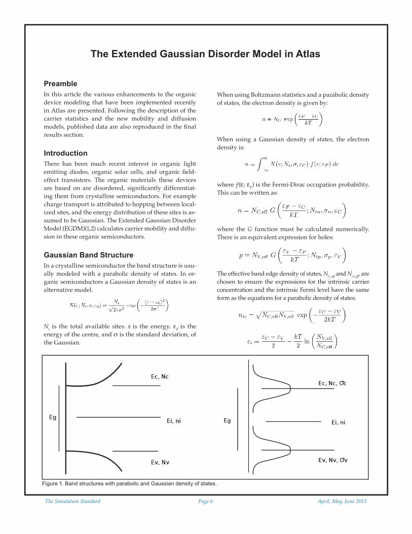
Introduction There has been much recent interest in organic light emitting diodes, organic solar cells, and organic fi eld-effect transistors. The organic materials these devices are based on are disordered, signifi cantly differentiat-ing them from crystalline semiconductors. For example charge transport is attributed to hopping between local-ized sites, and the energy distribution of these sites is as-sumed to be Gaussian. The Extended Gaussian Disorder Model (EGDM)(1,2) calculates carrier mobility and diffu-sion in these organic semiconductors.
Gaussian Band StructureIn a crystalline semiconductor the band structure is usu-ally modeled with a parabolic density of states. In or-ganic semiconductors a Gaussian density of states is an alternative model.
Nt is the total available sites. ε is the energy. ε0 is the energy of the centre, and σ is the standard deviation, of the Gaussian.
When using Boltzmann statistics and a parabolic density of states, the electron density is given by:
When using a Gaussian density of states, the electron density is:
where ƒ(ε; εF) is the Fermi-Dirac occupation probability. This can be written as:
where the G function must be calculated numerically. There is an equivalent expression for holes:
The effective band edge density of states, NC,eff and NV,eff, are chosen to ensure the expressions for the intrinsic carrier concentration and the intrinsic Fermi level have the same form as the equations for a parabolic density of states:
The Extended Gaussian Disorder Model in Atlas
Figure 1. Band structures with parabolic and Gaussian density of states.

April, May, June 2013 Page 7 The Simulation Standard
For energies several σ below the center of the Gaussian the function G has an exponential behavior, but as ε ap-proaches ε
0 the G curve saturates.
Various “universal” parameters associated with the Gaussian density of states are
• : the average distance between sites
• : the normalized carrier density
• : the normalized standard deviation of the Gaussian
• : a characteristic electric field
• : the normalized electric field
A Gaussian band structure can be defined in Atlas in the MATERIAL command
MATERIAL NTC.GAUSS=Nt,n SIGC.GAUSS=σn \
NTV.GAUSS=Nt,p SIGV.GAUSS=σp
The centre of the Lowest Unoccupied Molecular Orbital (LUMO) density of states is the electron affinity below the vacuum level (so that the centre of the LUMO level is the equivalent of the conduction band edge in a parabolic band structure), and the centre of the Highest Occupied Molecular Orbital (HOMO) density of states is the band gap below the centre of the LUMO density of states (so that the centre of the HOMO level is the equivalent of the valence band edge in a parabolic band structure).
The Pasveer MobilityThe Pasveer et al (1) mobility model has been implemented for the carrier hopping mobility in a disordered system with a Gaussian density of states. This has the following form:
In this paper the first two terms are written as:
However Atlas uses 300 K as the reference temperature so this is implemented as:
The expressions for the other factors are
with
and
In Atlas the Pasveer mobility model can be activated for electrons with the following parameters.
There are similar parameters for activating the model for holes.
MOBILITY PASVEER.N MUN=μ0,300 TC2.PASV.N=c2 \
CCUTOFF.N= n FCUTOFF.N= E
The CCUTOFF.N parameter defines the maximum value of n used in the calculation of g1, and the FCUTOFF.N parameter defines the maximum value of E used in the calculation of g2.
This makes it relatively easy to determine the effect of the individual terms in the Pasveer mobility. By setting CCUTOFF.N=0 and FCUTOFF.N=0 the g1 and g2 terms are both equal to unity (their limit at n = 0 and E = 0), and g0 is unity at 300 K. The following figure shows:
• g0 as a function of T (at a fixed n and E) for three different values of c2
• g1 as a function of n (at a fixed T and E) for four different values of σ
• g2 as a function of E (at a fixed T and n) for four different values of σ
Figure 2. Parabolic and Gaussian carrier concentration as a function of Fermi energy.
a = N 1/3t
n =ˆ nNt
σ=ˆ σkT
E0 =σqa
ˆ EE0
E =
ˆ ˆ
ˆ
ˆ ˆ
ˆ ˆ
ˆˆ
ˆ ˆ
ˆ
ˆ
Figure 3. The g0, g1, and g2 mobility factors as functions of, re-spectively, temperature, carrier density and electric field.

The Simulation Standard Page 8 April, May, June 2013
DiffusionThe diffusion coefficient is:
With a parabolic density of states and Boltzmann prob-ability statistics this gives:
This gives the standard Einstein diffusion coefficient:
For a Gaussian density of states and Fermi-Dirac probability statistics the differential is not as simple and the diffusion coefficient is written as a correction to the Einstein value
A simulation can be set up to extract the g3 parameter. The drift-diffusion current is:
If J=0 then:
If =0 then J=0 occurs as E=0 and this cannot be used to calculate the enhancement to the diffusion.
But if a built-in carrier gradient is introduced into the simulation, which can be performed with a graded dop-ing, then the field required to counteract the diffusion at zero current can be used to calculate g3.
ResultsVan Mensfoort and Coehoorn (2) give the results of some simulations on simple organic devices. The symmetrical device they model is 100 nm long with Schottky contacts on either end (the Schottky boundary conditions pin the Fermi level, and therefore the carrier density, at the con-tact). The LUMO density of states has Nt = 8.5 × 1020 cm-3, σ = 6, and μ0 = 1 × 10⁻⁶ cm2/Vs. The electron concentration at the contacts is n = 4.25 × 1020 cm-3, this is Nt/2 so the work functions of the contacts are at the middle of the LUMO level. This device can be created with the commands:
go atlas
mesh width=1e12
x.mesh loc=0 spac=0.25
x.mesh loc=1 spac=0.25
y.mesh loc=0 spac=0.001
y.mesh loc=0.1 spac=0.005
region number=1 material=organic
electrode name=anode top
electrode name=cathode bottom
material number=1 ntc.gauss=8.5e20 \
sigc.gauss=0.155 \
eg300=3 permittivity=3 affinity=1
contact name=anode workf=1
contact name=cathode workf=1
mobility mup=1e-6 mun=1e-6 pasveer.n
δnδx
Figure 4.The device has graded doping from the anode to the cathode, this gives a constant gradient in the electron concentration. This diffusion requires a built-in electric field to have zero current at zero bias. The middle graph is the diffusion enhancement factor, g3, as a function of carrier density for various widths of the Gaussian density of states.
ˆ

April, May, June 2013 Page 9 The Simulation Standard
The length in the x-direction is 1μm, the width of the de-vice is chosen to be 1012 μm (so that the xz-area is 1 m2 and the calculated current is equal to the current density). The affinity and the work-function of the contacts are the same value (so that the electron quasi-Fermi level at the contacts is in the middle of the LUMO level, and the resultant car-rier concentration is Nt/2). The band gap is large enough that the concentration of holes is insignificant.
ConclusionThe EGDM describes the mobility with:
and the diffusion coefficient with:
Gaussian density of states can be activated for the LUMO/HOMO levels with the command:
MATERIAL NTC.GAUSS=Nt,n SIGC.GAUSS=σn \
NTV.GAUSS=Nt,p SIGV.GAUSS=σp
and the Pasveer mobility model for electrons can be acti-vated with the command (similar parameters to activate the Pasveer model for holes):
MOBILITY PASVEER.N MUN=µ0,300 TC2.PASV.N=c2 \
CCUTOFF.N= n FCUTOFF.N= E
The g3 enhancement to the diffusion coefficient is cal-culated automatically due to the Gaussian density of states.
AcknowledgementsThis work was carried out under the ENLIGHTEN proj-ect (100838 – TP:16-127) and we thank the Technology Strategy Board (innovateuk.org) for their funding.
The assistance of Cambridge Display Technology (cdtltd.co.uk) and the Optoelectronics group at the University of Cambridge (oe.phy.cam.ac.uk) was gratefully received in the implementation of this model.
References1) Pasveer, W.F., et al, “Unified Description of Charge-Carrier Mobilities
in Disordered Semiconducting Polymers”, Physical Review Letters, (2005), PRL 94, 206601
2) van Mensfoort, S.L.M, & R.Coehoorn, “Effect of Gaussian disorder on the voltage dependence of the current density in sandwich-type devices based on organic semiconductors”, Physical Review B, (2008), 78, 085207-1
Figure 5. Atlas simulation of the 100 nm device reproducing figures 4a and 6b from reference 2.
ˆ ˆ

The Simulation Standard Page 10 April, May, June 2013
TCAD Simulation of Multiple Quantum Well Infrared Photodetector (QWIP)
AbstractWe demonstrate the capabilities of SILVACO TCAD tools for the design and simulation of intersubband GaAs/Al-GaAs multiple quantum well infrared photodetectors. We compute the photoconductive gain spectrum of the de-vice self consistently with the charge flow, non-radiative capture-escape, and intersubband transitions in the ac-tive region. The solid state calculations provide input to a light propagation modeling tool that allows for multiple reflections in the layered geometry of the active region. From this full calculation, we extract light absorption and quantum efficiency as a function of the angle of incidence and the wavelength of a mono-spectral beam of light. This TCAD simulation can be used as a starting point by de-sign engineers for obtaining guide lines to analyze and optimize quantum well infrared photodetectors.Keywords: Intersubband transitions, QWIP, Capture-Escape, k.p,
TCAD, Zincblende (z.b), Superlattice
IntroductionThe development of infrared photodetectors (IR) was started after the Second World War, and it has since been progressing at a rapid pace. Research in this field has al-ready made important technological impact in thermal imaging, night vision, and other IR applications. The first and second generation IR detectors exploited the intraband transitions, and were dominated by InSb and HgCdTe (also referred to as MCT). Both these materials could be used for detectors operating in the mid-wave-length regime (MWIR), with wavelength in the range of at 2-5 μm. The long-wavelength regime (LWIR) region is accessible only to MCT via its tailorable energy band gap over the range of 1–30 μm, large optical absorption for high quantum efficiency, and favorable intrinsic re-combination mechanisms. The MCT based IR technol-ogy is often considered matured. However uniformity and yield continue to be major limitations for MCT due to a weak Hg-Te bond that results in bulk, surface and interface instabilities. These limitations provide strong motivation to search for alternatives to MCT.
Multiple quantum well infrared detectors (QWIP) based on GaAs are an attractive alternative due to the well-de-veloped growth and processing technology. They have shown promising results, comparable with HgCdTe photodiodes at low temperatures in LWIR and very long wavelength regions (VLWIR). GaAs based QWIP tech-nology also provides the flexibility of monolithic inte-gration with GaAs electronics and into large focal plane arrays.
The principle underlying the operation of a QWIP is that of a quantum particle in a box. A set of quantum wells, with geometry and composition chosen to support only one bound state, collectively form a superlattice that supports a quasi-continuum of extended states carrying finite momentum. As a result, a bound state electron ex-cited into an extended state by a photon generates a finite photocurrent. Thus the bound to extended transitions form the fundamental absorption mechanism that deter-mines both the wavelength and the quantum efficiency of the detector. Perhaps the most attractive feature of a QWIP in this respect is the fact that absorption spectrum can be tuned by quantum well thickness and the barrier composition. On the other hand, the requirement of at least 30-50 wells in a single device is still a limiting fac-tor, which arises from the limited ability to control the growth over such thicknesses.
Technology Computer Aided Design by SILVACO pro-vides a flexible, cost-effective, and a rapid alternative for research and design optimization of QWIP. It allows re-searchers to gain insight into the complex physics inside a QWIP, and provides the ability to predict the material and geometrical parameters to create a device with the desired operating characteristics. This results in a signif-icantly more effective and efficient use of resources for device fabrication.
Simulation ConditionsThe structure of multiple quantum well we simulate consists of three GaAs quantum wells (n-type doped with concentration of 1.2×1018 cm-3), sandwiched between the wide band gap AlxGa1-xAs (x=0.25) layers, which act as barrier for the bound state carriers. The barriers should ideally be intrinsic, but we model them more realistically with n-type doping of 1011 cm-3. The thickness of quantum well is 4 nm, which we determined by lowering the thickness until only one bound state was supported. We chose the thickness of the barriers to be 50 nm to mini-mize the coupling of bound states in adjacent quantum wells, thereby making the wells virtually independent of each other. Inter-well coupling leads to inefficiencies due to increased radiative and non-radiative tunneling, and affects the spectrum in ways that are difficult to control as a function of electrical conditions. The structure of the active region and its electrostatic conditions may be directly compared with the middle of the 50 well region in the structure studied by Bethea et al [2].

April, May, June 2013 Page 11 The Simulation Standard
To bias the active region, we include 100 nm thick GaAs n-type contacts at the top and bottom of the active re-gion, and doped to the same concentration as the wells. The conduction band diagram with electron quasi-Fermi are shown in the Figure 1. In Figure 2, we show the pro-files of bound states acting as the initial states, and in Figure 3 we show the profile of a typical traveling state acting as the final state in optical absorption. The bound states decay sufficiently rapidly in the barriers that the well states can indeed be considered decoupled. In Figure 3 we note that the extended states are character-ized by highly oscillatory structure. Since the Schroding-er equation solves (see below) for the entire profile, these oscillations require a mesh with large spatial resolution.
We simulated 3 quantum wells instead of the full 50 well device in [2] because the large oscillations of quantum states require spatial resolution of less than 1 Angstrom, such that the simulation domain becomes limited by the
CPU, memory, and simulation time. However, this does not affect the conclusions reached in the simulation due to the fact that the quantum wells are independent to a very good approximation. Thus their optical response is additive. An additional difference arises from the fact that the quasi-continuum of extended states of the full device is replaced by a discrete spectrum in the smaller device modeled here. This is easily accounted for with a physically reasonable yet sufficiently large broadening of absorption line shape. Nonetheless, the users also have the ability to model absorption into a 1D continuum with its edge at the first extended state above each well.
We found from the simulation that the highly oscillatory nature of the extended states results in a very slow conver-gence of the magnitude of the optical transition matrix el-ements with respect to spatial resolution. This only affects the magnitude of the spectral response, while its shape converges rapidly at much coarser mesh spacing. Thus the meshes or nodes play a significant role for the accurate estimation of the range of detectable wavelengths, as well as the peak detection wavelength. The present simulation also provides an accurate estimate of quantum efficiency as a function of the incidence angle, taking into account both the fact that intersubband transitions are driven purely by TM modes (see below), as well as the effects of multiple reflections at material interfaces. Depending on the desired accuracy of magnitude of efficiency per well, users may need to further refine the mesh, resulting in longer simulation times.
The Schrodinger and Poisson equations may introduce non-linear corrections as the active region is lengthened. However, the electrostatic potential obtained from the self consistent solution provides us with a measure to gauge the importance of these corrections. This is so be-cause the potential essentially determines the location
Figure 2. Bound state wavefunctions in each of the three GaAs quantum wells. The wells support only one bound state.
Figure 3. The lowest travelling state wavefunction above the top of the leftmost quantum well. Note the abrupt phase shifts at well boundaries and the increasing oscillation frequency ap-proaching towards the collector. Both these require a high spa-tial resolution of the mesh.
Figure 1. Spatial profiles of conduction band edge and electron quasi Fermi level for a QWIP biased at 0.15 V. The structure consists of 3 GaAs quantum wells of thickness 4 nm separated by Al0.25GaAs0.75.

The Simulation Standard Page 12 April, May, June 2013
of energy levels and the wavefunction profiles, which in turn completely determine the intersubband transitions and absorption spectrum. From Figure 1 we note that the quasi Fermi-level shows a linear drop of 0.15 V across the active region, which translates to about 3 V across the 50 well counterpart of this active region. Thus the electro-static potentials relative to the well depth, and thus the Hamiltonians governing quantum states in each well, are expected to be similar in both cases.
Calculation MethodologyThe quantum well modeling, including its optical re-sponse, is activated by specifying the QWELL model for the quantum well regions. The model discretizes the Schrödinger equation along the direction specified by SP.GEOM, which in this case is along the length of the active region. The discretized equation is solved via the method of finite differences. The spatial dependence of effective mass is taken into account via the current con-servation boundary conditions.
The SLATT model activates the calculation of extended states over the union of regions for which this model is specified. This model also solves a discretized Schro-dinger equation, but the solutions at each energy satisfy boundary conditions of a plane wave of the same energy escaping into the contact regions. The effective mass and band edge parameters are derived from the multiband k.p model. The bound wavefunction is assumed to van-ish outside this range. Users have the option to set the wave function penetration length in microns via the WELL.MARGIN parameter. In the present case, the pen-etration length into barriers is 0.01 μm.
The carriers in the states above the barrier band edge comprise a current flow that is essentially 3D and semi-classical in nature. The carriers from these states are captured by bound states via phonon emission, and they escape from these bound states via phonon absorption. This in- and out-flow of carriers is included in the self consistent drift-diffusion model for the entire device by selecting the WELL.CAPT model, and is specified by a phenomenological time constant (WELL.TAUN) for carrier capture lifetime. This introduces an addi-tional balance equation between the 3D semi-classical and 2D quantum mechanical bound state densities. The WELL.CAPT model modifies the conduction and va-lance bands in the barrier region to avoid bound states at edges. The resulting coupled drift-diffusion, Poisson, and Schrödinger equations are all solved until self con-sistency is reached amongst them at each bias point.
The QWELL model automatically searches for all bound states, and includes in the optical response only up to a maximum of WELL.CNBS many states of the conduction subbands. If the number of bound states, say B, support-ed (as dictated by the Hamiltonian) is less than WELL.
CNBS, then all B bound states are reported. In the pres-ent case, we use this feature to verify that only one bound state is supported by physical conditions of well thickness and material affinities. We set WELL.CNBS=2, and then verify below (see Results and Discussion) that only one state is indeed reported. The users can adjust the barrier height via the AFFINITY parameter on the MATERIAL statement and also verify that more bound states appear in the results as barrier heights increase.
The multiple quantum well structure is illuminated by a black body source at room temperature. Planck’s for-mula completely specifies the spectral distribution of a black body in terms of the wavelength λ (in μm) and the temperature T (in Kelvin). The absorption of this light occurs via intersubband transitions from the bound to extended states in each quantum well, and the presence of WELL.CAPT parameter specifies this connection be-tween the QWELL and SLATT models.
To calculate the spectrally resolved absorption of long wavelength infrared radiation, the models consider the electromagnetic field to be a plane wave of frequency ω = 2πc/ λ. The coupling between the electronic states and the electric field, E, is described by the interaction Hamiltonian,
(1)
where dnm are the vectorial matrix elements of the dipole operator between the electronic states n,m. In the present simulation both n and m represent the different sub-bands of the same conduction band, in other words, the matrix elements dnm represent intersubband transitions.
When differences between the effective masses of the con-duction bands in the wells and the barriers do not change the wavefunctions significantly, the intersubband transi-tions yield dnm = dnm s, where s is the direction normal to the surface and dnm is the magnitude of the matrix element. Since s.E yields the TM component of E, we obtain the fa-miliar experimental fact that only the TM component of the incident light contributes to intersubband transitions. The steady state TM gain coefficient is extracted using the Fermi Golden rule, and takes the form,
(2)
Note that the gain formula as reported in literature is dif-ferent from the one in Eq. (2) in that the gain is expressed in terms of the photon energy associated with incident wave, instead of its frequency. Here, nr is the real part of refractive index, and is the dipole matrix element be-tween initial and final states, and in the direction perpen-dicular to the plane of the quantum wells. is the density of transverse states in two dimensions (a constant), and

April, May, June 2013 Page 13 The Simulation Standard
Γ is the line width due to Lorentzian broadening arising from the scattering of the electrons with lattice vibra-tions, as well as collisions with interface roughness. Em,n is the difference between energies En and Em of the initial and final subbands of the same carrier type respectively. fn and fm are the Fermi-Dirac distribution functions for the initial and final intersubband states, and integrated over the entire transverse energy range Et.
Equation (2) gives the number of photons with TM polar-ization generated by inter-subband electronic transitions per unit length. For a beam of light incident at an angle with respect to the normal to the well, the dependence of s.E on the incidence angle with the TM component of the field yields the final gain coefficient, which is also input to the optical propagation module, as
(3)
The factor of ½ in this formula arises from taking the beam to be unpolarized [2]. The incidence angle specifies only the plane of the electric field, and for a polarized beam for which the angle of the field within this plane is φ, the inner product |s.E|2=sin2(θ)cos2(φ). An unpolarized beam contains a uni-form distribution of all φ, so that integrating the gain over all cos2(φ) over 0 to 360 degrees produces the factor ½.
Results and DiscussionWe begin with a discussion of the electronic transitions. Figure 4 shows the TM gain for the device. Note that absorption is simply the negative of the gain, and it is clear from the figure that the device is absorptive over the entire range of wavelengths shown. The spectral bandwidth for absorption is approximately 2 μm, while the peak absorption occurs at approximately 10 μm. The spectral broadening in this calculation is 10 meV, and ab-sorption above each well is limited to 5 traveling states above the local barrier height.
Due to thermal excitation, a very small fraction of car-riers is expected to populate the extended states at 300 K, and contribute to dark current. The downward tran-sitions from these states to the bound states are domi-nated by phonons with a time constant WELL.TAUN = 1 ps. However, there is also very small contribution from emission of photons representing the reverse process of photocurrent generation. This radiative capture rate is spectrally resolved in Figure 5 and its integral with re-spect to energy yields a total radiative time constant of 100 ps. Thus we also confirm that, as is normal in QWIP systems, the radiative capture is of negligible importance compared to non-radiative capture emission included in the self consistent model.
The absorption results can be clearly interpreted in terms of the energies of the bound states, which in turn can be directly related to quantum well widths and material composition of barriers (in particular the barrier height). We can thus tune the peak detection wavelength by sim-ply adjusting the well width.
Figure 4. TM gain versus wavelength. Note that negative gain simply means positive abosroption of the same magnitude.
Figure 5. Spectrally resolved radiative capture rate, which when integrated over the shown energy range yields an effective time constant of about 100 ps.
Figure 6. Total absorption as a function angle of incidence for an unpolarized mono spectral beam of wavelength 10 µm. Note that the ratio of photocurrents represents quantum efficiency. The vertical axis is dimensionless.

The Simulation Standard Page 14 April, May, June 2013
We now show the results of total absorption of a mono spectral beam of light incident on this device at various angles and wavelengths. Figure 6 shows absorption and the ratio of available to source photocurrent as a func-tion of the angle of angle of incidence. The source pho-tocurrent is the incident beam power converted to units of electrical current, while the available photocurrent is the photocurrent generated by absorption. Thus in the absence of other loss mechanisms for IR photons, and the generated electrons, the ratio simply reproduces the absorption curve.
In Figure 6, the dependence of absorption on the angle of incidence θ shows the characteristic sin2(θ) form at small angles. We note that the maximum lies around 70 de-grees, and not at 90 degrees as would be expected from sin2(θ) alone. As the angle of incidence increases the beam propagates a greater distance along the surface, and thus a lower fraction interacts with the wells before being reflected back out of the device. The Luminous module in Atlas properly accounts for all the reflections to compute the actual angular dependence of the total absorption, and it clearly shows the expected drop in ab-sorption as compared sin2(θ) as incidence angles reach 60 degrees and beyond.
Figure 7 shows results of the calculation in which we vary the wavelength of the mono spectral beam while keeping its incidence angle at 30 degrees with respect to the normal. Here, as expected, we see that the total ab-sorption follows the gain curves since the intersubband transitions are the only source optical loss in the spectral range shown. The peak of the curve is again near 10 μm, and the curve follows the gain curve of the well nearest the optical source. Thus most of the total photocurrent is generated from this well.
We have assumed that all the photons absorbed in the quantum well excite the bound carriers and generate a photo current. The internal quantum efficiency of quantum well infrared detector can thus be computed by dividing the Source Photo Current to the Available Photo Current.
In the present simulation, only 3 wells are considered, and clearly, the maximum internal quantum efficiency η for these wells is very low. However, as pointed out above, addition of more wells would result in a linear increase in absorption with respect to the number of wells. This also explains why 50 or even more quantum wells are required to obtain a practical detector, as also reported in literature.
The spectral current responsivity of the quantum well infrared detector is the figure of merit and may be cal-culated from the gain and quantum efficiency data. The spectral current responsivity of QWIP is
(4)
Here, λ is the wavelength, η is the quantum efficiency, h is the Planck’s constant, c is the velocity of light, q is the electron charge, and G is the photoelectric current gain.
The dark current characteristics of a QWIP is shown in Figure 8 This can be performed by performing a series of simulations with the same bias voltage scan but different temperature specified on the models statement. The cur-rent plotted on a logarithmic scale is computed for a large bias range than in order to display its typical profile. Com-parison f the dark current curves for the present device at 77 K and 300 K shows the temperature dependency. The dark current is almost zero under zero bias condition, as biasing increases the current varies linearly. The curves clearly show the striking increase in dark current at high-er temperature. This results from the much higher ther-mal excitation at higher temperature. On the other hand, the differential dependence on the voltage remains very similar in both temperature regimes.
Figure 7. Total absorption as a function wavelength at the inci-dence angle of 30 degrees with respect to the normal. Note that the ratio of photocurrents represents quantum efficiency. The vertical axis is dimensionless.
Figure 8. Dark current as a function of bias voltage at low and high temperatures.

April, May, June 2013 Page 15 The Simulation Standard
The sensitivity of dark current to temperature also re-veals the further need for optimization with respect to the bound states. One the one hand, single bound state is necessary to ensure that all optical transitions generate a current, which increases efficiency. On the other hand, this also prevents us from having a deep bound state from which the thermal excitation can be suppressed even at high temperature. TCAD tools can be highly useful in finding an optimal balance between efficiency, detection wavelength, and dark current. Another prom-ising application of these tools is to search for alternative designs where these issues can be uncoupled and opti-mized independently.
Finally, we comment on various simplifications made in this simulation. We have neglected the effects tunneling assisted excitation, which further modify the response of the detector. The interface between the barriers and wells is taken to be ideal, i.e. without any interfacial de-fects or traps. The defect assisted tunneling is the major noise source in QWIP at low temperatures. We have not taken any noise into consideration in the above discus-sion. Users can incorporate the different types of noise associated with quantum wells using various noise models in the SILVACO model library. Finally, the resis-tance area product can be obtained by the differentiation of the dark current density with respect to voltage.
ConclusionWe demonstrated the use of SILVACO TCAD tools for design and optimization of quantum well infrared pho-todetectors based on GaAs in the long wavelength re-gion. We performed room temperature infrared absorp-tion, and dark current-voltage analysis. Although GaAs based QWIP technology has undergone aggressive de-velopment, improving the quantum efficiency remains a continuing challenge for researchers in this field. TCAD tools provide insight into the physical mechanisms plac-ing fundamental limitations on efficiency, and the ability to develop strategies to minimize their impact.
References1. B.F. Levine, G. Hasnain, G.B.Bethea & Naresh Chandra,
Appl. Phys. lett. 54 (26), pp. 2704 1989.
2. C.G.bethea, B.F.Levine, V.O. Shen, R.R.Abbott, S.J.Hseith, IEEE Trans Electron Dev., 38, pp. 1118, 1991.
3. P.K.Saxena, Infrared Physics & Technology, vol. 54, pp. 25–33, 2011.
4. Hyun-wook Shin, Kangsoo Kim & Jeong-woo Choe, Journal of the Korean Physical Society, 59 (1), pp. 150-155, July 2011.
5. ATLAS User’s Manual, Device Simulation Software, Silvaco International, Santa Clara, CA 95054.
.

The Simulation Standard Page 16 April, May, June 2013
Hints, Tips and Solutions
Q. How can I properly setup Athena Monte Carlo simulation of ion implantation in Silicon Carbide?
A. Monte Carlo module of Athena allows accurate simu-lation of ion implantation in 4H-SiC and 6H-SiC [1]. It is known that channeling effects are very pronounced in SiC since its lattice has several wide open channels ( e.g. 〈0001〉, 〈1120〉, and 〈1123〉 for 4H-SiC) and therefore im-plant profiles strongly depend on wafer orientation and ion beam direction. Another important aspect of ion im-plantation simulation in SiC is the fact that most of com-mercially available standard 〈0001〉 wafers are offered with miscut of 3.5° - 8.5° usually toward 〈1120〉 direction. The miscut is introduced primarily to facilitate epitaxial growth. In the same time the miscut alters ion implanta-tion, because implanting normal to the wafer surface is equivalent to a tilt of the beam in the (1120) plane.
In order to perform Monte Carlo implant simulation in Athena you should first specify simulation plane. The Monte Carlo module of Athena simulates ion trajectories in 3D and then registers the stopping points and con-sequently doping concentration by projecting 3D result onto simulation plane. The module also assumes that configuration of material interfaces don’t change in di-rection normal to this simulation plane. The simulation plane is always perpendicular to the wafer surface and its orientation is specified by parameter ROT.SUB in the the INITIALIZE statement relative to the wafer major flat (see Figure 1). To our knowledge most commercial 4H-SiC and 6H-SiC wafers have major flat parallel to (1100) plane as in Figure 1.
So, if you want your Athena simulation plane to be parallel to the major flat, 〈1100〉, you have to specify ROT.SUB=0. If you want your simulation plane to be parallel to 〈1120〉 crys-tallographic direction you should specify ROT.SUB=90.
The ion beam direction is specified by parameters TILT and ROTATION in the IMPLANT statement. The TILT is the angle (in degrees) between the ion beam vector and the normal to the wafer surface. The ROTATION is the angle between the ion beam vector plane perpen-dicular to the wafer surface and the simulation plane. For example, if the ion beam vector plane is parallel to 〈2110〉 crystallographic direction in Figure 1 you have to specify ROTATION=30 (see Figure 2). Alternatively, if the ion beam vector plane is perpendicular to simulation plane you have to specify ROTATION=90.
The wafer miscut is specified by parameters MISCUT.TH and MISCUT.PH. Parameter MISCUT.TH specifies the angle between actual wafer surface and the XZ plane (see Figure 1). Parameter MISCUT.PH specified the angle (measured counter-clockwise from the major flat direction) toward which the wafer was cut. So, if the wa-fer is cut toward <1100> (i.e. X direction in Figure 1) you need to specify MISCUT.PH=0. This type of miscut is not used very often. Majority of commercial wafers (see, for example, [2] and [3}) have miscut toward <1120>. So, practically in all cases you need to set MISCUT.PH=90 and MISCUT.TH=4 or MISCUT.TH=8 depending of “off axis” angle in commercial wafer specifications (see, [2] and [3]).
Figure 1. SiC wafer orientation relative to simulation plane in Athena BCA Module. Also shown are major plane projections on the wafer surface.
Figure 2. 3D SiC wafer and simulation plane orientation. ROT.SUB=0 for simulation plane parallel to (1100).

April, May, June 2013 Page 17 The Simulation Standard
Call for QuestionsIf you have hints, tips, solutions or questions to contribute,
please contact our Applications and Support Department Phone: (408) 567-1000 Fax: (408) 496-6080
e-mail: [email protected]
Hints, Tips and Solutions ArchiveCheck our our Web Page to see more details of this example
plus an archive of previous Hints, Tips, and Solutionswww.silvaco.com
So, a typical initialize of Monte Carlo implant statements will be as follows:
init sic_4h rot.sub=0implant aluminum energy=50 dose=1e13 bca n.ion=10000 tilt=4 rotation=90 miscut.th=4 miscut.ph=90
This will correspond to implant to a wafer with standard miscut usually specified as “Off axis 4° toward 〈1120〉 ± 0.5°” in commercial wafer specifications. The simulation plane will be parallel to the major flat, and ion beam will be tilted by 4 degrees in the plane perpendicular to the simulation plane.
The following examples closely demonstrate equivalent implant directions based on miscut MISCUT.TH/PH or TILT/ROTATION specifications.
EXAMPLE 1:This example demonstrates equivalent implant direc-tions with wafer’s major flat, 〈1100〉.
init sic_4h rot.sub=0
implant aluminum n.ion=40000 dose=0.63e13 tilt=0 rot=0 energy=60 bca
The equivalent implant direction with miscut wafer 4° 〈1120〉 toward will be
init sic_4h rot.sub=0
implant aluminum n.ion=40000 dose=0.63e13 tilt=4 rot=90 miscut.th=4 miscut.ph=90 energy=60 bca
The two profiles will be statistically equivalent with slight shift due to cos(4°) projection of the second profile.
EXAMPLE 2:This example demonstrates equivalent implant directions with wafer’s major flat, 〈1120〉. NOTE, MISCUT.TH/PH are measured from the internal crystallographic coordi-nate system, not the laboratory one defined by ROT.SUB.
init sic_4h rot.sub=90
implant aluminum n.ion=40000 dose=0.63e13 tilt=0 rot=0 energy=60 bca
The equivalent implant direction with miscut wafer 4° toward 〈1120〉 will be
init sic_4h rot.sub=90
implant aluminum n.ion=40000 dose=0.63e13 tilt=4 rot=0 miscut.th=4 miscut.ph=90 energy=60 bca
The two profiles will be statistically equivalent with slight shift due to cos(4°) projection of the second profile.
EXAMPLE 3:The following example demonstrates equivalent implant conditions for 3° tilted off [0001] direction toward 〈1120〉 implant for ideal, and for miscut 4° toward 〈1120〉 4H-SiC wafer.
init sic_4h rot.sub=0implant aluminum n.ion=40000 dose=0.63e13 tilt=3 rot=0 energy=60 bca
The equivalent implant direction with miscut wafer 4° toward 〈1120〉 will be
init sic_4h rot.sub=90
implant aluminum n.ion=40000 dose=0.63e13 tilt=1 rot=0 miscut.th=4 miscut.ph=90 energy=60 bca
The two profiles will be statistically equivalent with slight shift due to both profiles projection on the vertical, Y, coordinate.
References[1] I. Chakarov and M. Temkin, “Modeling of Ion Implantation in SiC
Crystals”, Nucl. Instr. And Meth. In Phys. Res. v. B-242, p.690, 2005.
[2] http://www.qualitymaterial.net/products.html
[3] http://www.semiconductorwafers.net/4H-Semi-insulating-SiC.html

The Simulation Standard Page 18 April, May, June 2013
Worldwide Offices: Silvaco Japan [email protected]
Silvaco [email protected]
Silvaco [email protected]
Silvaco [email protected]
Silvaco [email protected]
USA Headquarters:
Silvaco, Inc.4701 Patrick Henry Drive, Bldg. 2Santa Clara, CA 95054 USA
Phone: 408-567-1000Fax: 408-496-6080