silicon carbide technology for extreme environments db
TRANSCRIPT

Silicon Carbide Technology for Extreme
Environments
A THESIS SUBMITTED TO THE FACULTY OF SCIENCE,
AGRICULTURE AND ENGINEERING FOR THE DEGREE
OF DOCTOR OF PHILOSOPHY
by
Daniel Richard Brennan
BEng (Hons.), MSc
School of Electrical and Electronic Engineering
Newcastle University
United Kingdom
March 2015

i
Abstract With mankind’s ever increasing curiosity to explore the unknown, including a variety of
hostile environments where we cannot tread, there exists a need for machines to do
work on our behalf. For applications in the most extreme environments and applications
silicon based electronics cannot function, and there is a requirement for circuits and
sensors to be built from wide band gap materials capable of operation in these domains.
This work addresses the initial development of silicon carbide circuits to monitor
conditions and transmit information from such hostile environments. The
characterisation, simulation and implementation of silicon carbide based circuits
utilising proprietary high temperature passives is explored.
Silicon carbide is a wide band gap semiconductor material with highly suitable
properties for high-power, high frequency and high temperature applications. The
bandgap varies depending on polytype, but the most commonly used polytype 4H, has a
value of 3.265 eV at room temperature, which reduces as the thermal ionization of
electrons from the valence band to the conduction band increases, allowing operation in
ambient up to 600°C.
Whilst silicon carbide allows for the growth of a native oxide, the quality has limitations
and therefore junction field effect transistors (JFETs) have been utilised as the switch in
this work. The characteristics of JFET devices are similar to those of early thermionic
valve technology and their use in circuits is well known. In conjunction with JFETs,
Schottky barrier diodes (SBDs) have been used as both varactors and rectifiers.
Simulation models for high temperature components have been created through their
characterisation of their electrical parameters at elevated temperatures.
The JFETs were characterised at temperatures up to 573K, and values for TOV , β , λ ,
IS , RS and junction capacitances were extracted and then used to mathematically
describe the operation of circuits using SPICE. The transconductance of SiC JFETs at
high temperatures has been shown to decrease quadratically indicating a strong
dependence upon carrier mobility in the channel. The channel resistance also decreased
quadratically as a direct result of both electric field and temperature enhanced trap
emission. The JFETs were tested to be operational up to 775K, where they failed due to
delamination of an external passivation layer.

ii
Schottky diodes were characterised up to 573K, across the temperature range and values
for ideality factor, capacitance, series resistance and forward voltage drop were
extracted to mathematically model the devices. The series resistance of a SiC SBD
exhibited a quadratic relationship with temperature indicating that it is dominated by
optical phonon scattering of charge carriers. The observed deviation from a temperature
independent ideality factor is due to the recombination of carriers in the depletion
region affected by both traps and the formation of an interfacial layer at the SiC/metal
interface.
To compliment the silicon carbide active devices utilised in this work, high temperature
passive devices and packaging/circuit boards were developed. Both HfO2 and AlN
materials were investigated for use as potential high temperature capacitor dielectrics in
metal-insulator-metal (MIM) capacitor structures. The different thicknesses of HfO2
(60nm and 90nm) and 300nm for AlN and the relevance to fabrication techniques are
examined and their effective capacitor behaviour at high temperature explored. The
HfO2 based capacitor structures exhibited high levels of leakage current at temperatures
above 100°C. Along with elevated leakage when subjected to higher electric fields. This
current leakage is due to the thin dielectric and high defect density and essentially turns
the capacitors into high value resistors in the order of MΩ. This renders the devices
unsuitable as capacitors in hostile environments at the scales tested. To address this
issue AlN capacitors with a greater dielectric film thickness were fabricated with
reduced leakage currents in comparison even at an electric field of 50MV/cm at 600K.
The work demonstrated the world’s first high temperature wireless sensor node powered
using energy harvesting technology, capable of operation at 573K. The module
demonstrated the world’s first amplitude modulation (AM) and frequency modulation
(FM) communication techniques at high temperature. It also demonstrated a novel high
temperature self oscillating boost converter cable of boosting voltages from a
thermoelectric generator also operating at this temperature.
The AM oscillator operated at a maximum temperature of 553K and at a frequency of
19.4MHz with a signal amplitude 65dB above background noise. Realised from JFETs
and HfO2 capacitors, modulation of the output signal was achieved by varying the load
resistance by use of a second SiC JFET. By applying a negative signal voltage of
between -2.5 and -3V, a 50% reduction in the signal amplitude and therefore Amplitude
Modulation was achieved by modulating the power within the oscillator through the use
of this secondary JFET. Temperature drift in the characteristics were also observed,

iii
with a decrease in oscillation frequency of almost 200 kHz when the temperature
changed from 300K to 573K. This decrease is due to the increase in capacitance density
of the HfO2 MIM capacitors and increasing junction capacitances of the JFET used as
the amplifier within the oscillator circuit.
Direct frequency modulation of a SiC Voltage Controlled Oscillator was demonstrated
at a temperature of 573K with a oscillation frequency of 17MHz. Realised from an SiC
JFET, AlN capacitors and a SiC SBD used as a varactor. It was possible to vary the
frequency of oscillations by 100 kHz with an input signal no greater than 1.5V being
applied to the SiC SBD. The effects of temperature drift were more dramatic in
comparison to the AM circuit at 400 kHz over the entire temperature range, a result of
the properties of the AlN film which causes the capacitors to increase in capacitance
density by 10%.
A novel self oscillating boost converter was commissioned using a counter wound
transformer on high temperature ferrite, a SiC JFET and a SiC SBD. Based upon the
operation of a free running blocking oscillator, oscillatory behaviour is a result of the
electric and magnetic variations in the winding of the transformer and the amplification
characteristics of a JFET. It demonstrated the ability to boost an input voltage of 1.3
volts to 3.9 volts at 573K and exhibited an efficiency of 30% at room temperature. The
frequency of operation was highly dependent upon the input voltage due to the
increased current flow through the primary coil portion of the transformer and the
ambient temperature causing an increase in permeability of the ferrite, thus altering the
inductance of both primary and secondary windings. However due its simplicity and its
ability to boost the input voltage by 250% meant it was capable of powering the
transmitters and in conjunction with a Themoelectric Generator so formed the basis for
a self powered high temperature silicon carbide sensor node.
The demonstration of these high temperature circuits provide the initial stages of being
able to produce a high temperature wireless sensor node capable of operation in hostile
environments. Utilising the self oscillating boost converter and a high temperature
Thermoelectric Generator these prototype circuits were showed the ability to harvest
energy from the high temperature ambient and power the silicon carbide circuitry.
Along with appropriate sensor technology it demonstrated the feasibility of being able
to monitor and transmit information from hazardous locations which is currently
unachievable.

iv
Symbol Table
Barrier Height biφ
Charge of Electron q
Permittivity ε
Boltzmann constant k
P-N Grading Coefficient M
Forward bias depletion capacitance FC
Band Gap GE
Built in potential VJ
Zero bias junction capacitance CJO
Series resistance SR
Resistivity ρ
Drain current DI
Transconductance mg
Turn-off Voltage TOV
Channel length modulation parameter λ
Transconductance (SPICE) β
Gate-Drain Capacitance GDC
Gate-Source Capacitance GSC
Doping Concentration DN
Seebeck Co-efficient S
Electrical conductivity σ

v
Contents
Chapter 1: Introduction ................................................................................................................. 1
1.1 Background ......................................................................................................................... 1
1.2 Silicon Carbide Technology ............................................................................................... 2
1.3 Thesis Outline ..................................................................................................................... 3
Chapter 2: Literature Review ........................................................................................................ 5
2.1 Introduction ........................................................................................................................ 5
2.2 Silicon Carbide Properties .................................................................................................. 5
2.3 Silicon Carbide Devices ..................................................................................................... 7
2.3.1 Schottky Diodes .......................................................................................................... 7
2.3.2 SiC MESFET............................................................................................................... 8
2.3.3 SiC pin diode ............................................................................................................... 9
2.3.4 SiC JFET ..................................................................................................................... 9
2.3.5 SiC BJT ..................................................................................................................... 10
2.3.6 MOSFETs ................................................................................................................. 11
2.4 High Temperature Passives .............................................................................................. 12
2.4.1 High Temperature Resistors ...................................................................................... 12
2.4.2 High Temperature Capacitors ................................................................................... 13
2.4.3 High Temperature Inductors ..................................................................................... 14
2.4.4 Packaging and Circuit Boards ................................................................................... 14
2.5 Silicon Carbide Circuits .................................................................................................... 14
2.5.1 Power Circuits ........................................................................................................... 14
2.5.2 Signal level circuits ................................................................................................... 17
2.6 Silicon Carbide Integrated Circuits .................................................................................. 18
2.7 Silicon Carbide Based Oscillators .................................................................................... 20
2.8 Hostile Environment Energy Harvesting .......................................................................... 22
2.8.1 Harvesting Energy from Light .................................................................................. 23
2.8.2 Harvesting Energy from Heat.................................................................................... 23
2.8.3 Harvesting Energy from Vibration ............................................................................ 24
2.8.4 Energy Storage .......................................................................................................... 24
2.8.5 Energy Management Circuits .................................................................................... 25
2.9 Integration Challenges ...................................................................................................... 25
2.9.1 MEMs Sensors .......................................................................................................... 26
2.9.2 Diode Sensor ............................................................................................................. 26

vi
2.9.3 Capacitive Sensors .................................................................................................... 27
2.10 Conclusions .................................................................................................................... 28
2.11 References ...................................................................................................................... 29
Chapter 3: Silicon Carbide Electronic Devices ........................................................................... 33
3.1 Introduction ...................................................................................................................... 33
3.2 Experimental ..................................................................................................................... 33
3.2.1 The ideal diode .......................................................................................................... 33
3.2.2 The depletion region .................................................................................................. 35
3.2.3 Extraction of Schottky diode parameters for SPICE simulation ............................... 37
3.2.4 Experimental extraction of Schottky diode parameters for high temperature SPICE
simulation ........................................................................................................................... 39
3.3 Silicon Carbide Junction Field Effect Transistors ............................................................ 43
3.3.1 JFET DC Characteristics ........................................................................................... 44
3.3.2 Extraction of JFET SPICE Parameters ...................................................................... 50
3.3.3 High Temperature JFET Characteristics ................................................................... 56
3.4 High Temperature Passive Components ........................................................................... 58
3.4.1 High Temperature Capacitors ................................................................................... 58
3.4.2 High Temperature Resistors ...................................................................................... 64
3.5 Properties of metals at High Temperature ........................................................................ 65
3.6 High temperature magnetic components .......................................................................... 66
3.6.1 High Temperature Spiral Inductors ........................................................................... 67
3.7 Conclusions ...................................................................................................................... 69
3.8 References ........................................................................................................................ 70
Chapter 4: Silicon Carbide Electronic Oscillators ...................................................................... 72
4.1 Introduction ...................................................................................................................... 72
4.2 Experimental ..................................................................................................................... 72
4.2.1 The Electronic Oscillator .......................................................................................... 72
4.2.2 The nonlinear oscillator ............................................................................................. 72
4.3 Linear oscillators .............................................................................................................. 73
4.3.1 Negative resistance oscillators .................................................................................. 73
4.3.2 The feedback oscillator ............................................................................................. 75
4.3.3 Crystal oscillators ...................................................................................................... 76
4.3.4 RC Oscillators ........................................................................................................... 77
4.3.5 LC Oscillators ........................................................................................................... 77
4.3.6 The Colpitts Oscillator .............................................................................................. 79
4.4 High Temperature Colpitts Oscillator .............................................................................. 84
4.4.1 High Temperature Voltage Controlled Oscillator ..................................................... 85
vii
4.5 Modulation........................................................................................................................ 88
4.5.1 High temperature Amplitude Modulation ................................................................. 90
4.5.2 High Temperature Frequency Modulation ................................................................ 97
4.6 Conclusions .................................................................................................................... 100
4.7 References ...................................................................................................................... 102
Chapter 5: Energy Harvesting in Extreme Environments ......................................................... 104
5.1 Introduction .................................................................................................................... 104
5.2 Experimental ................................................................................................................... 105
5.2.1 Energy harvesting technologies............................................................................... 105
5.2.2 Vibrational Energy Harvesting ................................................................................ 105
5.2.3 Photovoltaics ........................................................................................................... 106
5.2.4 Thermoelectric harvesters ....................................................................................... 107
5.3 Step Up Converter .......................................................................................................... 110
5.3.1 Continuous mode operation .................................................................................... 112
5.3.2 Discontinuous mode operation ................................................................................ 114
5.4 A Novel high temperature boost converter ..................................................................... 116
5.5 Blocking Oscillator ......................................................................................................... 117
5.5.1 Theory of JFET blocking oscillator without RC network ....................................... 120
5.6 Self oscillating boost converter ...................................................................................... 123
5.6.1 High temperature SOBC prototype ......................................................................... 126
5.7 Conclusions .................................................................................................................... 130
5.8 References ...................................................................................................................... 131
Chapter 6: Conclusion ............................................................................................................... 134
6.1 Future Work .................................................................................................................... 136

1
Chapter 1: Introduction
1.1 Background
Hostile environments surround us, they include those which are man made in the case of
combustion engines, or natural such as the interior of volcanoes or even the surface of other
planets. As electronic circuits have rapidly developed, science has been able to monitor and
shed light on ever more extreme locations. With the emergence of wide bandgap
semiconductors it is now possible to once again shift the boundaries of the monitored world.
These wide bandgap materials are revolutionising electronics. As an example, we can build ultra
bright GaN LED’s providing multi-million dollar savings through reduced energy consumption.
In the power and aerospace industries, SiC can be utilised to provide smaller power modules,
thus saving space and through life costs. In mobile communication systems, GaN transistors can
achieve higher power densities and frequencies than conventional silicon devices, allowing for
our ever hungry data requirements to be met. Ultimately they allow us to build devices which
outperform silicon in a wide range of applications.
One such application, which is becoming more relevant in a number of fields, is that of high
temperature electronics. Due to the bandgap of silicon being 1.12eV at room temperature, the
thermal generation of electron – hole pairs in the bulk of the silicon devices renders them
inoperable at temperatures above 150°C. In an attempt to combat this, Silicon on Insulator
(SOI) technology has been developed, but even this only operates to 275°C. Wide bandgap
materials such as silicon carbide (SiC) have a significantly larger badgap 3.26eV at room
temperature for the 4H polytype, enabling operation at temperatures over 600°C.
There are multiple locations and processes that can be enhanced through better monitoring and
control, which require the utilisation of high temperature electronics. These include combustion
engines, power generation, jet engines and a variety of industrial processes. High temperature
electronics and sensors also have a potential application in volcano plumes to monitor the
composition of gas species emitted from the volcano and potentially give an early warning of a
potential eruption. Silicon carbide also has the potential to increase our scientific knowledge of
the surface of other planets, such as Venus and Mercury and the magnetosphere of Jupiter. All
of these places share the same problem they are hot, hostile environments where people cannot
survive. As a result any electronics placed there must be self sufficient in terms of power and
include the means of communication for the data to a safer location.
In addition to active silicon carbide devices, all circuits require passive devices to operate.
These passives include resistors, capacitors and inductors. Whilst some commercial devices are

2
available, these are aimed primarily at the oil and gas/defence industries, where applications are
looking for temperature ratings approaching 300°C. Hence, there is a requirement for research
into both passive components for high temperature operation and suitable packing/printed
circuit boards for high temperature electronics.
This work addresses the initial development of silicon carbide circuits to monitor conditions and
transmit information from such hostile environments. The characterisation, simulation and
implementation of silicon carbide based electronic circuits and their passive component
counterparts are explored with a view to creating high temperature energy harvesting wireless
sensor nodes.
1.2 Silicon Carbide Technology
Silicon carbide (SiC) is wide bandgap semiconducting material with a high breakdown electric
field strength, high saturated electron drift velocity and a thermal conductivity better than
copper at room temperature. These properties make it desirable and suitable for use in high-
power, high-frequency and high temperature applications. An extremely hard substance with a
Young’s modulus of 424 GPa, SiC is chemically inert, reacting very little with any known
material at room temperature. It can be etched using molten KOH at 400-600°C or with reactive
ion etching. Dopants must be implanted or grown into the material as diffusion, the technique
preferred in silicon processing, is impossible within a production environment due to the
extremely high temperatures required and the speed at which diffusion takes place.
The bandgap of silicon carbide depends upon polytype with a value of 3.265 eV in the case of
4H-SiC, which is the most commonly used polytype and is utilised in this work. Due to its wide
bandgap the thermal ionization energy required to move electrons from the valence band to the
conduction band if much greater and as a result silicon carbide is electrically operable at
temperatures above that possible with silicon. Like other semiconductors it is possible to make a
range of devices including diodes, Junction Field Effect Transistors (JFET), Metal
Semiconductor Field Effect Transistor (MESFET), Metal Oxide Semiconductor Field Effect
Transistor (MOSFET), Bipolar Junction Transistor (BJT) for the realisation of electronic
circuits. Whilst the majority of research into SiC has focussed on the requirements of the power
industry, due to the ability to control high levels of energy in small volumes and at higher
frequency, resulting in a cost saving at system level, smaller amounts of research have been
conducted into building signal level devices.
These signal level devices are often lateral in contrast to the vertical structures utilised in power
devices. This allows the integration of a large number of devices on a single SiC die, thus
paving the way for integrated circuits. The potential of integrated circuits shows great promise

3
for the future of silicon carbide as a material for high temperature electronics. As these
integrated circuits develop in complexity, digital electronics will increase from the example of
gate and flip-flop structures currently demonstrated into far more complex systems and
ultimately microprocessors capable of operation in extreme environments. Ultimately the
techniques learnt from silicon processing can be transferred to silicon carbide allowing it to be
scaled relatively quickly. There are however issues with native SiO2 have to be solved for high
temperature MOSFET’s and the variability of wafer defects and doping profiles are examples of
limiting factors which have impeded it progress.
1.3 Thesis Outline
Chapter 2 presents a review of the current literature in the relevant fields. It described the
unique material properties of silicon carbide with relation to the operation of devices which
have high temperature, high power and high frequency capabilities. The chapter explores the
current technological maturity of silicon carbide, in terms of both the discrete devices which can
be fabricated and are already commercially available and research grade integrated circuits
which have been demonstrated. Insight is provided into the various high temperature passive
devices required for high temperature circuits along with both packaging and circuit board
technologies. The chapter provides an overview of the different power circuits, which can be
easily constructed from silicon carbide components and highlights the importance of oscillator
circuits in electronic systems for wireless communications. Energy harvesting technologies
which are compatible with silicon carbide technology are explored to provide power to silicon
carbide electronics in hostile environments. Finally, integration of these high temperature
components into a working system is considered.
Chapter 3 provides an in depth analysis of silicon carbide active components and high
temperature passives. It explores in detail both the physical and electrical operation of the SiC
components utilised in the construction of the high temperature circuits commissioned in this
work. The chapter demonstrates the characterisation of active silicon carbide components and
how these values are incorporated into mathematical models for utilisation in SPICE to aid in
the simulation and development of high temperature electronics. Also explored are high
temperature passive components, including resistors, capacitors and inductors, and how these
were characterised for use at elevate temperature in hostile environments
Chapter 4 presents an overview of oscillator circuit topologies and describes their functionality.
It focuses on LC oscillator circuits, specifically the Colpitts oscillator and its usage in the
creation of high frequency sine waves specifically for radio frequency purposes. It provides an
in depth description of the Colpitts oscillator operation and how it can be modelled using

4
negative resistance theory. The results presented in this chapter demonstrate the world’s first
Amplitude Modulation (AM), Frequency Modulation (FM) and Voltage Controlled Oscillator
(VCO) circuitry built from silicon carbide and high temperature passive components operating
at high temperatures. These circuits provide the basis for communications from a silicon carbide
wireless sensor node within a hostile environment and provide the functionality to transmit data
to a safer location for dissemination.
Chapter 5 presents an overview of the challenges faced in powering a high temperature wireless
sensor node in a hostile environment. It explores the usage of high temperature energy
harvesting solutions as an alternative to the equally immature high temperature battery
technologies. The chapter concentrates on thermoelectric generators as the choice of energy
harvest as there is often an excess ambient thermal energy in high temperature environments
provided there is a temperature gradient. The theories of the main power circuit topologies are
explored and their operation explained. A novel self oscillating SiC boost converter topology is
presented which is able to boost the voltage levels of low voltage - high current sources such as
thermoelectric generators and photovoltaic cells. The boost converter is demonstrated to be
operational at high temperatures and capable of boost low voltages to those required to power a
SiC wireless sensor node.
Chapter 6 presents the conclusions drawn from this research; it explores possible avenues for
future work and the great potential that silicon carbide technology presents in the area of high
temperature electronics.

5
Chapter 2: Literature Review
2.1 Introduction
Hostile environment is a generic term used to describe locations that could be dangerous or even
lethal to humans. In some cases, scientific observations and measurements of these
environments are lacking due to their hazardous nature. Despite these facts, hostile
environments are common place and pervade our everyday lives. Examples of such can be
commonplace such as automotive combustion engines or can be much more exotic such as
space applications or exploration of foreign planets. Generally the term hostile environment is
applied to locations of extreme temperature range and/or elevated radiation flux.
Following the invention of the transistor and subsequent rapid advancement in electronics that
has followed, humans have been able to shed light on ever more dangerous territory. However
silicon (Si) technology has its limitations, and in recent years we have seen the emergence of
new wide band gap semiconductors, capable of deployment in areas and conditions which
would cause silicon electronics to fail. In addition to research and development of these new
wide band gap materials capable of such tasks, there has been a drive in the development of self
powered electronics eliminating the requirements of wires or batteries. These two distinct areas
of research converge to allow the creation of self powered sensor nodes for use in hostile
environments.
2.2 Silicon Carbide Properties
Silicon carbide (SiC) is wide bandgap semiconducting material with a high breakdown electric
field strength, high saturated drift velocity of electrons and a high thermal conductivity. These
properties make it suitable for use in high-power, high-frequency and high temperature
applications.
An extremely hard substance with a Young’s modulus of 424 GPa, SiC is chemically inert
reacting very little with any known material at room temperature[1]. It can be etched using
molten KOH at 400-600°C or with reactive ion etching. Dopants must be implanted or grown
into the material as diffusion is practically impossible.
The bandgap depends upon polytype with a value of 3.265 eV at room temperature in the case
of 4H-SiC, which is the most commonly used variant and is utilised in this work [2]. Due to its
wide bandgap, thermal ionization of electrons from the valence band to the conduction band,
which limits the overall highest electronically operable temperature of a semiconductor, doesn’t
6
occur until far greater temperatures than silicon and is therefore suitable for these hostile
applications.
In the case of power applications, SiC boasts high breakdown electric field strength maxE . This
property determines the largest electric field the material can be subjected to before catastrophic
breakdown occurs. maxE is typically quoted as roughly 2MV/cm close to ten times that of
silicon.[3] SiC also exhibits a saturation drift velocity twice that of silicon, with a value of 2 x
107cm/sec. [4, 5]. This is extremely advantageous in order to obtain high channel currents for
microwave devices and therefore SiC is an ideal material for high-gain solid-state devices.
Important to both power and high frequency devices, SiC also has a thermal conductivity of
5W/(cm-K) which is higher than copper at room temperature [6,7]. As an increase in device
temperature results in a decrease in carrier mobility which degrades device performance and so
the heat generated through resistive losses must be conducted into packaging away from the
device.
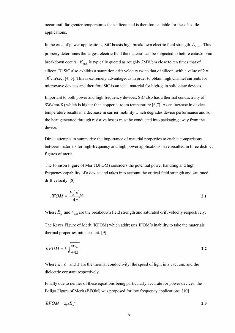
Direct attempts to summarize the importance of material properties to enable comparisons
between materials for high-frequency and high power applications have resulted in three distinct
figures of merit.
The Johnson Figure of Merit (JFOM) considers the potential power handling and high
frequency capability of a device and takes into account the critical field strength and saturated
drift velocity. [8]
2 2
24B SatE v
JFOMπ
= 2.1
Where BE and Satv are the breakdown field strength and saturated drift velocity respectively.
The Keyes Figure of Merit (KFOM) which addresses JFOM’s inability to take the materials
thermal properties into account. [9]
4Satcv
KFOM kπε
= 2.2
Where k , c and ε are the thermal conductivity, the speed of light in a vacuum, and the
dielectric constant respectively.
Finally due to neither of these equations being particularly accurate for power devices, the
Baliga Figure of Merit (BFOM) was proposed for low frequency applications. [10]
3BBFOM Eεµ= 2.3

7
Where µ is the carrier low-field mobility. To indicate SiC’s potential the two most common SiC
polytypes are compared with Si and GaAs in the table below with all values normalised to Si.
[3]
Material JFOM KFOM BFOM
Si 1 1 1
GaAS 9 0.41 22
6H-SiC 900 5 920
4H-SiC 1640 5.9 1840
2.3 Silicon Carbide Devices
SiC can be doped by both ion implanted and/or grown with both n and p type dopants, and due
to the possibility of native oxide growth, like silicon a range of electronic devices can be
fabricated from this semiconducting material. As described in section 2.1 the superior properties
of SiC in comparison to Si has resulted in the majority of the literature to concentrate on power
devices. In this work small scale test power devices were utilised as small signal devices which
are operational at elevated temperatures.
Firstly we will consider metal-semiconductor devices namely the Schottky barrier diode (SBD)
and Metal-Semiconductor Field Effect Transistor (MESFET), before moving through p-n
barrier devices such as the pn diode, JFET and Bipolar Junction Transistor (BJT) and
concluding with the less mature oxide technologies of the Metal Oxide Semiconductor Field
Effect Transistor (MOSFET).
2.3.1 Schottky Diodes
The SiC Schottky barrier diode (SBD) was the first commercially available SiC power
semiconductor device. Arguably they are also one of the first semiconductor devices fabricated
known as point rectifiers or cat whiskers [11].
The main advantage of Schottky diodes is the elimination of reverse recovery charge ( rrQ ) that
is the dominant cause of the switching losses in bipolar Silicon PiN power diodes. Schottky
diodes are majority carrier devices hence they do not require a reverse recovery current to

8
discharge the minority carriers in the depletion region. SiC SBDs outperform their Si
counterparts by providing lower on-resistance and significant reduction in switching time. Due
to the high maxE of SiC it is possible to fabricate power devices with high maximum blocking
voltages suitable for use in the power applications [3].
Minimised switching and conduction power losses are required in high performance power
converter applications. To reduce the conduction loss of the power Schottky diode without
compromising the device blocking voltage, the Schottky barrier height can be reduced by
utilising different metal semiconductor junctions. This, however, causes higher leakage currents
during the reverse bias of the power diode. Currently commercial SiC Schottky diodes are
available from a number of manufacturers including Cree, Infineon, Microsemi, IXYS, Rohm
and STMicroelectronics.
Figure 2.1 Schematic of a Schottky Barrier Diode
2.3.2 SiC MESFET
Another common device using the metal-semiconductor junction is the MESFET. MESFETs
are usually constructed in compound semiconductor technologies lacking high quality surface
passivation, although SiC has the ability to grow a native SiO2 its quality although improving,
has its limitations particularly at high temperature.
MESFETs offer processing and performance advantages over the JFET. The process of
fabricating metal gates can be achieved at lower temperatures in comparison to a p-n junction
implantation anneal sequence and offers the potential to define short channel lengths for high
speed applications. The low gate resistance and low IR drop along the channel width is a big
factor in microwave performance such as noise and maximum frequency of oscillation (fmax). As
a result they are commonly employed in high frequency, high power applications such as
RADAR and satellite communications. [3]

9
Figure 2.2 Schematic structure of a MESFET
2.3.3 SiC pin diode
As silicon carbide allows for both the ion implantation and introduction of dopants during
crystal growth, it is possible to fabricate devices incorporating p-n junctions. The simplest of
these devices is the p-n junction diode. In contrast to SBDs which exhibit ultra high speed
characteristics p-n junction diodes are minority carrier devices and therefore have a greater
reverse recovery time. Diodes based on pn junctions can also be used as light emitting diode’s
(LEDs), which allows for optical based communications, and can also be used as UV
photovoltaic cells, thus allowing energy harvesting from UV light. [Ref]
Figure 2.3 Schematic of PiN diode
2.3.4 SiC JFET
By utilising the properties of p-n junctions it is possible to fabricate a variety of different
electrical devices the two of main importance are the JFET and BJT. JFETs have similar

10
characteristics to MESFETs and are discussed more thoroughly in chapter 3. Their advantage
over metal-semiconductor technology is a more robust junction resulting in higher breakdown
and power handling capabilities. Due to issues with traps and poor quality metal oxide interface
the junction of a JFET is simpler to fabricate than an equivalent MOSFET in SiC technology. In
SiC it is possible to fabricate both normally on (depletion mode) and normally off (enhancement
mode) JFETs. p-type depletion mode JFET have also been demonstrated but suffer due to the
poor hole mobility in p-type SiC. [12]
Both vertical power and lateral signal level devices have been demonstrated in the literature and
remain operational to high temperatures with high reliability [13]. JFETs were the first
commercially available switching device fabricated from SiC and are now offered by multiple
companies. Whilst Normally-off JFET’s are desirable for simplicity of design in switching
circuits for power electronics; normally-on JFETs have their advantages in a range of
applications, including energy harvesting applications, as discussed in chapter 5.
Figure 2.4. Schematic structure of a JFET
2.3.5 SiC BJT
The Bipolar Junction Transistor (BJT) is named because their operation involves both electrons
the majority charge carriers in n-type semiconductor and holes the majority carriers in p-type
semiconductor. Alternative structures either p-n-p or n-p-n are available and charge flow in
these devices is due to diffusion of charge carriers across this junction.
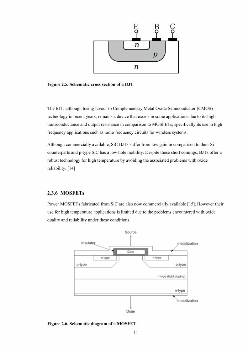
11
Figure 2.5. Schematic cross section of a BJT
The BJT, although losing favour to Complementary Metal Oxide Semiconductor (CMOS)
technology in recent years, remains a device that excels in some applications due to its high
transconductance and output resistance in comparison to MOSFETs, specifically its use in high
frequency applications such as radio frequency circuits for wireless systems.
Although commercially available, SiC BJTs suffer from low gain in comparison to their Si
counterparts and p-type SiC has a low hole mobility. Despite these short comings, BJTs offer a
robust technology for high temperature by avoiding the associated problems with oxide
reliability. [14]
2.3.6 MOSFETs
Power MOSFETs fabricated from SiC are also now commercially available [15]. However their
use for high temperature applications is limited due to the problems encountered with oxide
quality and reliability under these conditions.
Figure 2.6. Schematic diagram of a MOSFET

12
When a voltage is applied to the gate of a MOSFET with reference to the Source, of sufficient
magnitude to switch the device an inversion layer is created beneath the gate connecting the
drain and source through which current is able to flow.
The MOSFET is the most important device for the realisation of high-density integrated circuits
such as microprocessors and semiconductor memories. Both JFET and MOSFETs have
significantly higher input impedance than BJT’s this allows them to be utilised in the standard
microwave systems. Because there is no forward biased p-n junctions, MOSFETs do not suffer
from minority-carrier storage and as a result have higher switching speeds then devices which
require minority carriers. In addition the devices are square law or linear devices (discussed in
chapter 3) and as a result intermodulation and cross-modulation products are smaller than those
of BJTs.
2.4 High Temperature Passives
In addition to active SiC devices high temperature circuits also require passive components and
high temperature packaging/circuit boards. This section gives a brief overview as
characterisation of such devices is covered in chapter 3.
2.4.1 High Temperature Resistors
High temperature resistors can either be fabricated directly out of a semiconducting material
thus allowing them to be on-chip creating highly integrated circuits or they can be stand alone
discrete components.
In the case of integrated components the most commonly used method for creating SiC resistors
on chip is through the process of ion implantation. By doping a semiconductor with an impurity
opposite to that of the native substrate it is possible to control the resistance. Examples of this
are available in the literature in both in Si technology and SiC. [16, 17]
The advantages of on chip resistors allows for both a smaller circuit footprint, approaching that
possible in Si technology, but also allows for the temperature coefficient of resistors to match
the active devices on the same die. [17] There are disadvantages to intergrated resistors which
include using space on the die, and also heating. Resistors can also be fabricated from pure
metallic wires with a known temperature coefficient. Metal film resistors possess good noise
characteristics and low non-linearity due to a low voltage coefficient and also demonstrate a
small tolerance, temperature coefficient and good stability. [18]

13
In addition to metal films, resistors can also be fabricated from metal oxides. Metal oxide
resistors such as those fabricated from tin oxide are capable of high temperature operation and
provide a higher level of reliability and stability in such applications. [19]
2.4.2 High Temperature Capacitors
Arguably the most complex and difficult component to fabricate for high temperature
applications is the capacitor. Simple small radio frequency (RF) capacitors can be fabricated
directly on chip/circuit board by utilising an interleaved comb structure. [20]
To create larger capacitors a dielectric is required to be sandwiched between two capacitor
plates thus creating a parallel plate capacitor. Much literature can be found surrounding metal
insulator metal (MIM) capacitors for their usage in numerous applications and multiple methods
of fabrication have been investigated. [21]
Figure 2.7 Schematic of a Metal-Insulator-Metal capacitor
The main complexities that plague high temperature capacitors are both the leakage current and
defects along with the relative dielectric constant of the insulator. To reduce a capacitor’s
physical dimensions whilst maintaining its electrical value the thickness of the insulating layer
must be reduced. However this reduction in insulator thickness results in increased leakage
currents which can arise from multiple mechanisms. These include transmission of leakage
current along grain boundaries, carbon contamination, and pin hole defects.
Another method of increasing capacitance is by altering the insulator material. Hafnium Oxide
HfO2 for example is a high-k dielectric which allows the use of thicker layers whilst
maintaining capacitance density. This material exhibits excellent thermal stability and shows
great promise for high temperature capacitor applications. [22]

14
2.4.3 High Temperature Inductors
Perhaps the most simple of the passive devices is the high temperature inductor. Small RF
inductors can be fabricated in multiple shapes out off metallic tracks on a circuit board as
described in chapter 3 and the literature. [23]
Higher inductances become more problematic at higher temperatures due to them generally
requiring a ferrite core. There are multiple examples of ferrite materials to be found in the
literature and commercially available ferrites with high curie temperatures are also available.
[24]
It is difficult to control the inductance of such high temperature inductors due to the changes in
ferrite material permeability with temperature. In this work a high Curie temperature ferrite
from Ferrox Cube was employed as its curie temperature was stated as approximately 350°C. At
higher temperatures still there is also nano-grain materials which demonstrate higher curie
points. [25]
2.4.4 Packaging and Circuit Boards
At high temperatures parasitic resistance becomes of greater concern as does a specific metals
tendency to oxidise or diffuse. As a result precious metals such as gold have to be utilised as
they do not oxidise with high temperature [26]. In this work the passive devices had gold
contacts, the wire bonds were also gold along with circuit board traces and IC packaging.
Fabrication of circuit boards for high temperature can be expensive if utilising gold for such
temperature extremes and therefore electroplating of gold was employed to thicken tracks and
thus lower their parasitic resistance. Electroplated gold can also be utilised to plate cheaper
metals to provide a passive high temperature barrier.
2.5 Silicon Carbide Circuits
2.5.1 Power Circuits
Due to the superior properties of silicon carbide in comparison to silicon as described in section
2.1, the majority of research surrounding SiC is aimed at the power electronics industry where
savings can be made by utilising SiC technology to increase efficiency and reduce losses along
with reducing overall space requirements.
The main area of research surrounding the use of silicon carbide components within the
literature is the application of SiC devices within power converter circuits, specifically DC-DC

15
converters. The definition of a DC-DC converter is a circuit which converters a DC current to
either a higher or lower voltage. Typical DC-DC converters consist of a diode, a switching
element and a magnetic storage component (inductor). Multiple topologies exist however they
are all based on the basic three traditional technologies. The three fundamental DC-DC
converter topologies are the Buck, Boost and Buck-Boost converters.
The buck (step-down) converter is a DC-DC converter that regulates the output voltage to a
lower level than its input voltage. As shown in figure 2.8, the current through the inductor
increases when the switch is in the on-state. When the switch is closed, the diode conducts and
the inductor current decreases as the stored energy in the output inductor drops. As the output
inductor reduces the output current ripple, the output capacitor directly limits the ripple in the
output voltage. The output voltage of the buck converter is calculated using equation 2.4.
on
O in in
tV V DV
T= = 2.4
Where 1Tf
= the switching period, ont is the switch on-state time, and ont
DT
= is the duty
cycle.
Figure 2.8. Buck Converter topology
The boost (step-up) converter is a DC-DC converter that regulates the output voltage at a level
greater than the input voltage. The energy stored in the input inductor increases when the switch
is in the on-state. When the switch is off, the diode conducts and the current flows from the
input-source through the inductor to the load. The input voltage source in series with the input
inductor behaves like a current source. As both the discharge-current in the inductor and the
input voltage source are supplying the load during the switch off-state, the voltage across the
load is larger than the input voltage alone. As there is no inductor in the output, the output
capacitor needs to be sufficiently large to reduce the output voltage ripple and maintain a

16
constant output voltage [27]. The boost converter topology is shown in figure 2.9 and its output
voltage can be calculated using equation 2.5.
Figure 2.9. Boost converter topology
1
1O in in
on
TV V V
T t D=
− − 2.5
The buck-boost converter is a DC-DC converter that can regulate the output voltage at a level
lower or greater than the input voltage. Here, depending on the duty cycle, the converter can act
as a boost or buck converter. When the switch is off, the diode conducts and the inductor limits
the output current ripple. The output capacitor can directly limit the output voltage ripple similar
to the buck converter. The output voltage polarity in the buck-boost converter is the opposite of
that of the input voltage. This topology is shown in figure 2.10 and its output voltage can be
calculated using equation 2.6.
Figure 2.10 Buck-Boost Converter topology
1on
O in in
on
t DV V V
T t D= − =
− − 2.6
As can be seen from the data in figures 2.8 – 2.10, power circuits can be commissioned from
commercially available components, hence the abundance of literature surrounding the

17
properties of these topologies. However the majority of the literature focuses upon efficiency at
room temperature and the potential of silicon carbide circuits to operate at higher temperatures
have been under investigated [28]. One feature of all of the topologies described in this thesis is
they require some form of switch waveform to operate as converters. This important aspect is
often overlooked in high temperature applications and it is obvious that circuitry to produce this
waveform must also be able to operate at elevated temperatures.
2.5.2 Signal level circuits
In contrast to the interest in SiC power devices, there has been significantly less focus on signal
level SiC devices for use in high temperature environments. These should not be overlooked as
they play an important role alongside their high current counterparts in the construction of
completely stand alone operational SiC circuits. The majority of research conducted in this area
has been by the NASA Glenn research centre and has utilised the also common polytype 6H as
opposed to 4H utilised in this work. Most signal level devices are lateral channel devices as
opposed the vertical channel devices commonly employed for power applications. This allows
multiple devices to be placed and connected on a single SiC die a step towards more complex
integrated circuit applications. [29] Further work in this area has also seen the emergence of the
first integrated operational amplifier. [17]
Figure 2.11 Silicon carbide lateral signal JFET [30]

18
The devices shown in the above figure 2.11 were shown to operate reliably at 500°C, and they
were utilised to demonstrate simple logic gate configurations and also amplifier structures
which pave the way for both more complex analogue and digital integrated circuits. The devices
durability is down to the numerous protective oxides protecting the surface of the JFET.
2.6 Silicon Carbide Integrated Circuits
Recent reports in the literature have reported the initial development towards Integrated circuits
(IC) on SiC substrates utilising JFET, MOSFET and MESFET devices. Multiple structures have
been demonstrated including both digital logic and analogue amplifiers. Whilst p-type SiC
remains problematic due to its low hole mobility, the literature shows that it is possible to
fabricate CMOS from silicon carbide and due to the advances and lessons learnt through silicon
processing IC technology fabricated solely from SiC may be in the not too distant future. [31]
Figure 2.12 Circuit schematics of (a) JFET inverter, (b) JFET NAND gate, (c) JFET NOR
gate. [31]
Shown in figure 2.12 are examples of basic JFET logic circuits utilising an active load topology
popular in early silicon NMOS technology dating back to the early 1980’s. The absence of p-
type material allows for higher device performance. [32]

19
Similar structures have been demonstrated in MESFET technology [33] and also CMOS
MOSFET technology [34]. In the case of CMOS technology more complex structures were
designed and fabricated utilising the simple gate structures to create both flip-flops and ring
oscillators.
Figure 2.13 Schematic of a SiC CMOS ring oscillator [34].
The early illustrations of digital electronics fabricated from SiC indicates that more complex
circuitry such as microprocessors and other advanced systems could eventually be fabricated
from SiC allowing for complex electronics capable of operation in hostile environments.
Along with digital electronics there have also been examples of integrated analogue electronics
such as amplifier structures which would allow for more robust signal conditioning and
collection from sensors. [17]
20
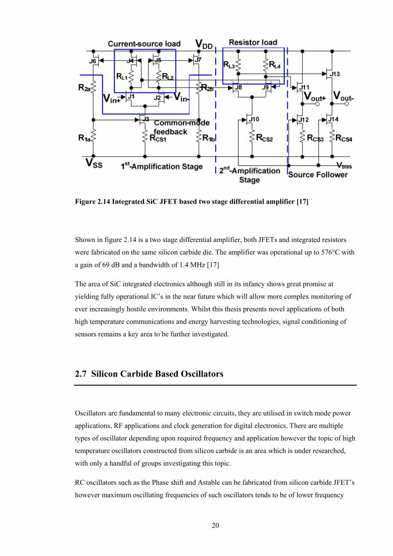
Figure 2.14 Integrated SiC JFET based two stage differential amplifier [17]
Shown in figure 2.14 is a two stage differential amplifier, both JFETs and integrated resistors
were fabricated on the same silicon carbide die. The amplifier was operational up to 576°C with
a gain of 69 dB and a bandwidth of 1.4 MHz [17]
The area of SiC integrated electronics although still in its infancy shows great promise at
yielding fully operational IC’s in the near future which will allow more complex monitoring of
ever increasingly hostile environments. Whilst this thesis presents novel applications of both
high temperature communications and energy harvesting technologies, signal conditioning of
sensors remains a key area to be further investigated.
2.7 Silicon Carbide Based Oscillators
Oscillators are fundamental to many electronic circuits, they are utilised in switch mode power
applications, RF applications and clock generation for digital electronics. There are multiple
types of oscillator depending upon required frequency and application however the topic of high
temperature oscillators constructed from silicon carbide is an area which is under researched,
with only a handful of groups investigating this topic.
RC oscillators such as the Phase shift and Astable can be fabricated from silicon carbide JFET’s
however maximum oscillating frequencies of such oscillators tends to be of lower frequency

21
and for higher frequency oscillations used in RF transmission LC and Crystal oscillators are
used instead.
Oscillators generally consist of a parallel inductive and capacitive (LC) network called a tank
circuit, an active amplifying device and a power source. The combination of an ideal LC circuit
with no losses would see electrical power continuously exchanged between the inductive and
capacitive elements at their combined resonant frequency given by
1
2f
LCπ= 2.7
In real circuits there are always loses and the need for an amplifing device is required to sustain
the oscillations. In the case of high temperature circuits this can be any form of SiC amplifying
transistor or a negative resistance device such as an IMPATT diode.
There are multiple types of oscillator but the main ones to consider are the Hartley, Colpitts, and
negative resistance oscillator these along with others are discussed in further depth in chapter 4
but are shown in figure 2.15.
Figure 2.15. (a) Hartley Oscillator. (b) Colpitts Oscillator (c) Negative resistance oscillator
Numerous variations of oscillators can be constructed from these three main types. The
literature is abundant with numerous examples of oscillators dating back to thermionic valve
theory [35].
Impact-ionization-avalanche-transit-time (IMPATT) diodes are an example of negative
resistance oscillators. IMPATT diodes are able to transmit power at millimetre-wave
frequencies, and are widely used in ultra high frequency transmitters such as those employed in
radar and communication systems. [36]

22
The peak output power of an IMPATT diode at a given frequency is limited by its underlying
material properties. Due to SiC’s high breakdown field and high electron saturation velocity the
peak power capability of the SiC IMPATT diode is expected to be at least two orders of
magnitude higher than the existing silicon and gallium arsenide IMPATT diodes [37].
Also discussed previously was the potential RF capability of MESFET technology the most
prominent examples in the literature include a 1GHz SiC Clapp oscillator which is a variant of
the Colpitts family, a cross coupled MESFET oscillator which operated up to 450°C, and
30MHz and 90MHz MESFET Clapp oscillators which operated at 450°C and 470°C
respectively. All of the above operated with commercially available Cree MESFET transistors
[38, 39, 40].
There is little information in the literature regarding crystal based oscillators despite SiO2 being
operable at elevated temperature. Crystal oscillators such as the Pierce oscillator have great
frequency stability with temperature variation. Temperature variation specifically the variation
in component values and hence the operating frequency of oscillation is also under reported.
In this work we demonstrate three types of high temperature oscillator. Two are based on a
common Colpitts oscillator topology designed specifically with high temperature RF
communications in mind whilst the other is based on a blocking oscillator for power
applications. Furthermore we effectively demonstrate Amplitude modulation (AM) and
Frequency modulation (FM) techniques for the first time at high temperature. [41, 42]
In the case of the FM oscillator, it was direct frequency modulation and can also be considered
an example of a high frequency voltage controlled oscillator which could be used not only to
transmit data through FM modulation but also as a technique to stabilize frequency over varying
temperatures.
2.8 Hostile Environment Energy Harvesting
Energy harvesting is an area of research gaining much attention for standard silicon electronics
as the advantages of not having to replace batteries in devices is appealing in many applications.
In the case of hostile environments energy harvesting is a prerequisite as it is simply not
possible to replace batteries. There are multiple types and methods of harvesting electrical
energy depending upon the ambient source this energy must then be stored in some form of
medium whether it be a battery or capacitor technology.

23
2.8.1 Harvesting Energy from Light
Perhaps the most mature energy harvesting technique is the use of photovoltaic cells. Whilst
usually produced from silicon and other low temperature semiconductor materials for
converting light in the visible spectrum. It is possible to fabricate photovoltaic cells from SiC
which would enable high temperature operation.
Figure 2.16. Cross sectional schematic of a photovoltaic cell
As shown in figure 2.16, ultra violet light striking the cell raises the energy level of electrons
and frees them from their atomic shells. The electric field at the pn junction drives the electrons
into the n region while the positively charged holes are driven to the p region. A metal grid or
Transparent conducting oxide on the surface of the cell collects the electrons while a metal
back-plate collects the positive charges.
Reported in the literature is SiC’s ability to harvest ultra violet light, whilst significantly less
efficient than its silicon counterparts due to defects and limitations in current wafer quality it
has been shown that it is capable of effectively harvesting energy at elevated temperatures. [43]
2.8.2 Harvesting Energy from Heat
Converting waste heat into electrical energy is also a well known method of power generation.
As SiC devices are capable of high temperature operation, this may be the most prudent
technology and is therefore further discussed in Chapter 5.
Thermoelectric generators (TEG’s)like photovoltaic cells are manufactured from n and p type
semiconductors as shown in figure 2.17.
24
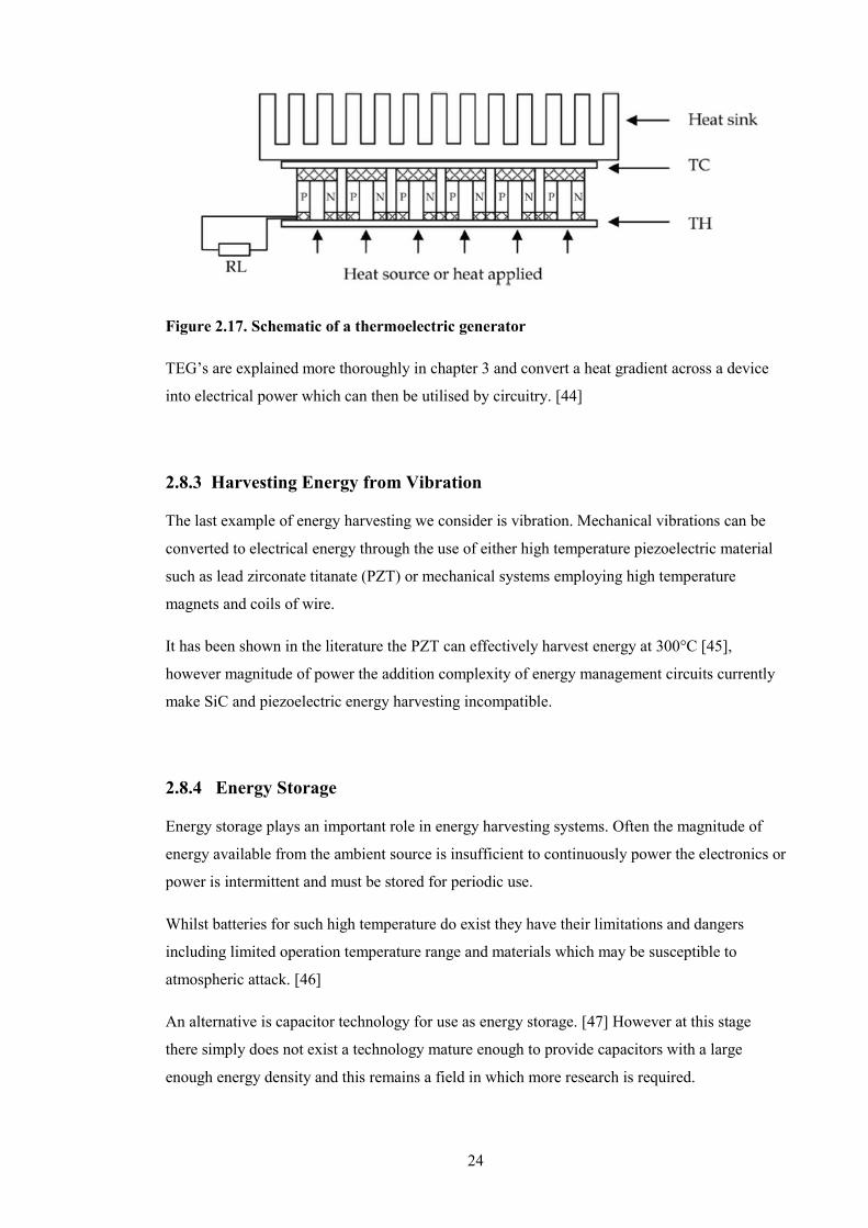
Figure 2.17. Schematic of a thermoelectric generator
TEG’s are explained more thoroughly in chapter 3 and convert a heat gradient across a device
into electrical power which can then be utilised by circuitry. [44]
2.8.3 Harvesting Energy from Vibration
The last example of energy harvesting we consider is vibration. Mechanical vibrations can be
converted to electrical energy through the use of either high temperature piezoelectric material
such as lead zirconate titanate (PZT) or mechanical systems employing high temperature
magnets and coils of wire.
It has been shown in the literature the PZT can effectively harvest energy at 300°C [45],
however magnitude of power the addition complexity of energy management circuits currently
make SiC and piezoelectric energy harvesting incompatible.
2.8.4 Energy Storage
Energy storage plays an important role in energy harvesting systems. Often the magnitude of
energy available from the ambient source is insufficient to continuously power the electronics or
power is intermittent and must be stored for periodic use.
Whilst batteries for such high temperature do exist they have their limitations and dangers
including limited operation temperature range and materials which may be susceptible to
atmospheric attack. [46]
An alternative is capacitor technology for use as energy storage. [47] However at this stage
there simply does not exist a technology mature enough to provide capacitors with a large
enough energy density and this remains a field in which more research is required.

25
2.8.5 Energy Management Circuits
Each of the discussed forms of energy harvesting technologies discussed in this section require
their own specific energy management circuits. Discussed in chapter 4 is a novel boost
converter for use with low voltage high current sources such as photovoltaic’s and TEG’s. But
Piezoelectric and electromagnetic source provide magnitudes of power which are too low to be
efficiently managed by current SiC Technology. Currently there exists no literature in the realm
of self powered energy harvesting silicon carbide sensor nodes.
2.9 Integration Challenges
As discussed SiC wireless sensor nodes face substantial challenges ranging from energy
harvesting to fabricating devices and circuits capable of operation in such extreme
environments. Another important aspect to be considered is the integration of the various
electronic components whether discrete or ICs are used circuit boards and packaging must be
commissioned which is able to with stand these hostile environments.
Figure 2.20. Illustration of integrated components wireless sensor node.
As shown in figure 2.20, there are multiple parts which are currently researched individually
that are required in the commissioning of a high temperature wireless sensor node. These
include energy harvesting, power regulation and conversion, sensors, analogue/digital signal
conditioning, communication circuitry and a means of transmitting this information to a safe
location.
With regards to packaging and PCBs a high temperature insulating material must be used the
most popular being AlN and Al2O3 which are both stable at high temperatures. For PCB
interconnects gold seems the most appropriate metal to be used as it is none reactive in most
environments, has good conduction characteristics, and a high melting point and a well known
change in resistance with temperature. Gold however is an expensive and traditional methods
26
employed to etch excess copper from PCBs is not a viable option electrochemical deposition or
printing of gold followed by an appropriate anneal stage are far less wasteful and therefore
appear to be promising alternatives.
Commissioning a high temperature wireless sensor node requires high temperature compatible
sensors, multiple examples of SiC sensors can be found in the literature [48], but can be
separated into three main types Micro Electrical Mechanical (MEM) sensors, diode sensors and
capacitor sensors.
2.9.1 MEMs Sensors
Micro Electrical Mechanical sensors include accelerometers and pressure sensors, they are
miniature mechanical devices which must be fabricated by etching and or machining processes.
In the case of silicon carbide this can be extremely costly due to its material properties and lack
of suitable etches, therefore sensors made from silicon carbide must provide advantages over
other substrates, one such advantage is their ability to operate at much higher temperatures.
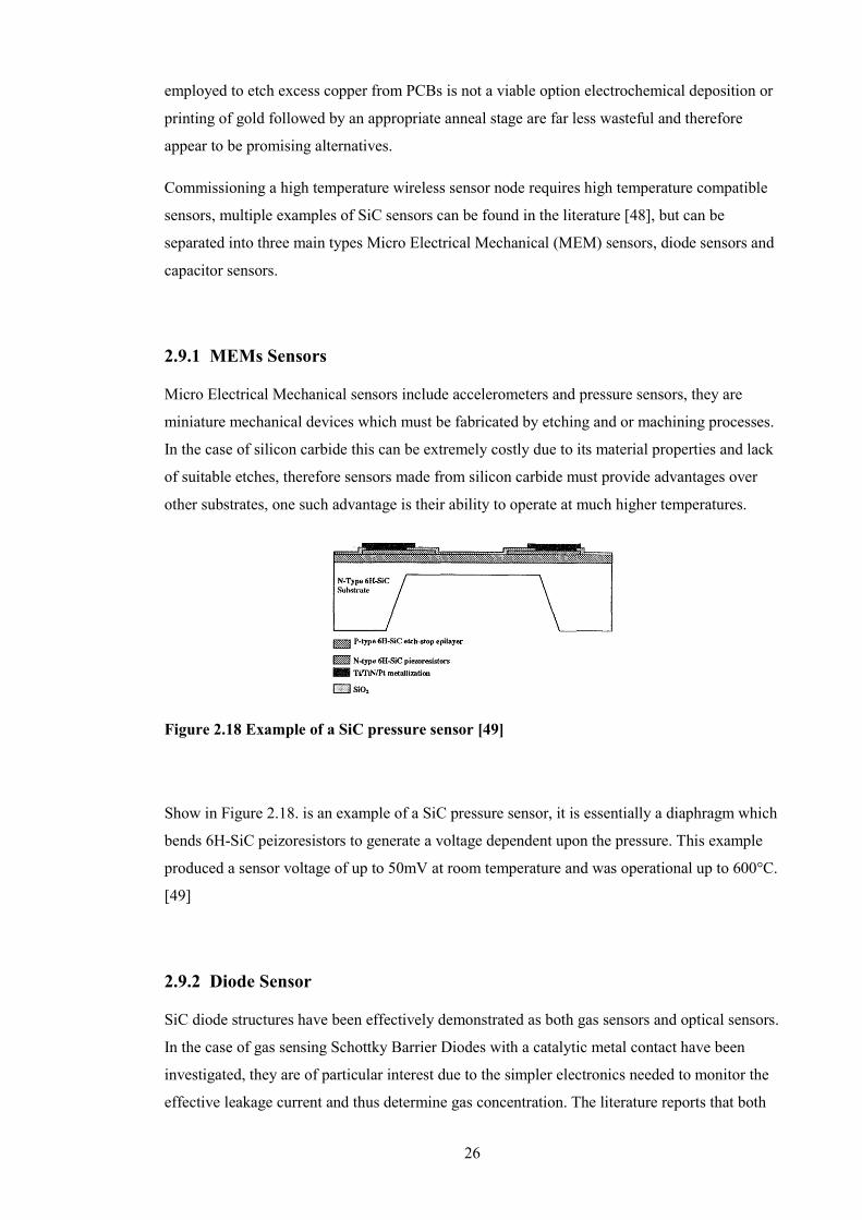
Figure 2.18 Example of a SiC pressure sensor [49]
Show in Figure 2.18. is an example of a SiC pressure sensor, it is essentially a diaphragm which
bends 6H-SiC peizoresistors to generate a voltage dependent upon the pressure. This example
produced a sensor voltage of up to 50mV at room temperature and was operational up to 600°C.
[49]
2.9.2 Diode Sensor
SiC diode structures have been effectively demonstrated as both gas sensors and optical sensors.
In the case of gas sensing Schottky Barrier Diodes with a catalytic metal contact have been
investigated, they are of particular interest due to the simpler electronics needed to monitor the
effective leakage current and thus determine gas concentration. The literature reports that both

27
Pd and Pt Schottky diodes can effectively be used to detect both methane and hydrogen with an
increased efficiency at higher temperatures. [50]
Silicon carbide diodes have also been demonstrated as both Ultra Violet (UV) and X-ray
detectors. In the case of UV detectors silicon carbide p-n junctions can be fabricated which are
only sensitive to radiation with a wavelength below 365 nm and are often referred to as visibly
blind as are unaffected by visible light wavelengths. UV diodes can be used to detect fire and
spark events along with various other scientific uses.
Traditional solid-state x-ray detectors, such as silicon and germanium, are cooled, often to 77 K
in order to reduce their noise for use in energy spectroscopy [51]. In contrast wide bandgap
semiconductor materials, such as silicon carbide, do not require cooling for their operation.
Silicon carbide offers a number of advantages, namely, in the provision of semiconductor
fabrication technologies, such as epitaxial growth and commercial wafer supplies, which will be
critical for the fabrication of multi-pixel arrays. [52]
2.9.3 Capacitive Sensors
Metal–Insulator–SiC (MISiC) devices offer a versatile fabrication structure in which both the
catalytic metal and the insulating material can be specifically chosen to be responsive to various
gaseous species.
Figure 2.19 (a) Schematic picture of an MISiC device with a dense catalytic metal gate. (b)
A porous catalytic metal gate structure. [3]

28
There has been a great deal of research into gas sensors utilising silicon carbide as they can be
operated in extreme environments such as exhaust flumes’, combustion engines, and other high
temperature environments. They have been shown to effectively detect hydrogen and hydrogen
containing species, along with ammonia and oxygen. Arrays of capacitor structures with
varying catalytic metals and alternative insulating layers can be fabricated for detecting a range
of various gases on a single die. Along with the appropriate analogue and digital electronics also
discussed previously the electronic noses allow for a better understanding of the nature of
certain hostile environments.
The circuitry needed to condition the signals from these sensors is an area under investigation as
indicated by sections 2.4 and 2.5 appropriate signal level devices and IC’s are beginning to
emerge. Powering a silicon carbide sensor node is also a challenge and the basic circuit
topologies and energy harvesting technologies are explored in sections 2.5 and 2.8. The
transmission of information to a safe location requires oscillators for either wireless or optical
communications and these are explored in section 2.7. Ultimately whilst there has been
individual research in each of these areas the challenges faced in combining the different
circuitry into a final module have not been addressed and require future research and
development.
2.10 Conclusions
This chapter has given an overview of silicon carbide properties and current silicon carbide
technology, along with the complimentary high temperature passive devices and packaging
required to commission high temperature circuitry for hostile environments. It has outlined the
current research ongoing in the field of both power devices and circuitry with a bias
concentrating on lower power signal level devices and IC’s.
The literature has shown that it is possible to fabricate both high temperature analogue and
digital circuitry whether from discrete devices and associated high temperature passives but also
indicated that there is a drive towards the integration of such devices into SiC IC’s. It has also
reported upon the various sensor technologies which can also be fabricated from SiC and able to
operate alongside their electronic counterparts.
Also investigated was the use of energy harvesting technologies for use in extreme
environments allowing for perpetual measurements to be taken with no need for high
temperature battery technology this allows for wireless sensor nodes to be placed permanently
in hostile environments.
29
The literature reviewed in this work forms the background for the research conducted in the rest
of this thesis. The advancements in silicon carbide along with passive and packaging
technologies have been considered with a view to commissioning a prototype high temperature
wireless sensor node.
2.11 References
[1] Matus, L. G., et al., Inst. Phys. Conf. Ser., No 137, 1993, p. 185–188.
[2] Choyke, W. J., and G. Pensl, “Physical Properties of SiC,” MRS Bulletin, March 1997,
pp.25–29.
[3] Advances in Silicon Carbide Processing and Applications, Stephen E. Saddow, Anant
Agarwal.
[4] Allen, S. T., et al., “Recent Progress in SiC Microwave MESFETs,” Mat. Res. Symp. Proc.,
Vol. 572, 1999, pp. 15–22.
[5] Järrendahl, K., and R. Davis, “Material Properties and Characterization of SiC,
Semiconductors and Semimetals,” SiC Materials and Devices, Vol. 52, Y. S. Park, (ed.), 1998
[6] http://www.cree.com/Products/sic_silicarb.html
[7] Slack, G. A., J. Appl. Phys., Vol. 35, 1964, p. 3460.
[8] Johnson, E. O., RCA Rv., Vol. 26, 1965, p. 163.
[9] Keyes, R. W., Proc. IEEE, Vol. 60, 1972, p. 225.
[10] Baliga, B. J., J. Appl. Phys., Vol. 53, 1982, p. 1759
[11] Flowers, A. E., Crystal and Solid Contact Rectifiers, No. 5, 1908, p. 445.
[12] Silicon Carbide: Volume 2: Power Devices and Sensors, Volume 2, Peter Friedrichs,
Tsunenobu Kimoto, Lothar Ley, Gerhard Pensl
[13] Philip G. Neudeck et al, IEEE Electron Device Letters, Vol. 29, No.5, May 2008 p. 456
[14] Yi Tang; Fedison, J.B.; Chow, T.P., "High temperature characterization of implanted-
emitter 4H-SiC BJT," in High Performance Devices, 2000. Proceedings. 2000 IEEE/Cornell
Conference on , vol., no., pp.178-181, 2000
[15] http://www.cree.com/Power/Products/MOSFETs

30
[16] Siedel T. E., IEEE Transactions on Electronic Devices, Vol. Ed-20, No. 8, August 1973 p.
744
[17] Patil A. C., IEEE Custom Intergated Circuit Conference, 2009
[18] J.J. Van Den Broek, J.J.T.M. Donkers, R.A.F. Van Der Rijt, J.T.M. Janssen, Metal film
precision resistors: Resistive metal films and a new resistor concept, Philips Journal of
Research, Volume 51, Issue 3, 1998, Pages 429-447.
[19] Q.X. Jia, Z.Q. Shi, K.L. Jiao, W.A. Anderson, F.M. Collins, Reactively sputtered RuO2
thin film resistor with near zero temperature coefficient of resistance, Thin Solid Films, Volume
196, Issue 1, 1 February 1991, Pages 29-34,
[20] Chang-Sheng Chen; Yo-Shen Lin; Wei-Ting Chen; Chin-Sun Shyu; Shinn-Juh Lay; Min-
Lin Lee, "PCB embedded capacitor with central via connection structure for RF application,"
Advanced Packaging and Systems Symposium, 2008. EDAPS 2008. Electrical Design of , vol.,
no., pp.77,80, 10-12 Dec. 2008
[21] Ching-Sung Ho; San-Jung Chang; Shih-Chang Chen; Liou, J.J.; Hongge Li, "A Reliable
Si3N4/Al2O3-HfO2 Stack MIM Capacitor for High-Voltage Analog Applications," Electron
Devices, IEEE Transactions on , vol.61, no.8, pp.2944,2949, Aug. 2014
[22] Bing Miao, Radiation Induced Change in Defect Density in HfO2 Based MIM Capacitors,
IEEE Transactions on Nuclear Science, 2009
[23] Burghartz, J.N.; Rejaei, Behzad, "On the design of RF spiral inductors on silicon," Electron
Devices, IEEE Transactions on, vol.50, no.3, pp.718,729, March 2003
[24]http://www.maginc.com/File%20Library/Product%20Literature/General%20Information/C
G-06.pdf
[25] www.ferroxcube.com/FerroxcubeCorporateReception/datasheet/4c65.pdf
[26] High Temperature Electronics, Randall Kirschman, IEEE Press
[27] M. H.Rashid, Power Electronic Handbook: Academic Press, 2001.
[28] Bhatnagar P, Wright NG, Horsfall AB, Johnson CM, Uren MJ, Hilton KP, Munday AG,
Hydes AJ, High temperature applications of 4H-SiC vertical junction field-effect transistors and
Schottky Diodes, 6th European Conference on Silicon Carbide and Related Materials, vol 556-
557, p. 987-990

31
[29] Philip G. Neudeck, Steven L. Garverick, David J. Spry, Liang-Yu Che, Glenn M. Beheim,
Michael J. Krasowski, and Mehran Mehregany, Extreme temperature 6H-SiC JFET integrated
circuit technology, Phys. Status Solidi A 206, No. 10, 2329–2345 (2009)
[30] Philip G. Neudeck, David J. Spry, Liang-Yu Chen, Glenn M. Beheim, Robert S. Okojie,
Carl W. Chang, Roger D. Meredith, Terry L. Ferrier, Laura J. Evans, Michael J. Krasowski, and
Norman F. Prokop, Stable Electrical Operation of 6H–SiC JFETs and ICs for Thousands of
Hours at 500C, IEEE electron device letters, Vol. 29, No. 5, May 2008
[31] David T. Clark, Robin F. Thompson, Aled E. Murphy, David A. Smith, Ewan P. Ramsay,
Robert A. R. Young, Craig T. Ryan, Sean Wright and Alton B. Horsfall, CMOS Circuits on
Silicon Carbide for High Temperature Operation, Proceeding of the MRS 2014.
[32] Chia-Wei Soong, Amita C. Patil, Steven L. Garverick, Xiaoan Fu, and Mehran Mehregany,
550 C Integrated Logic Circuits using 6H-SiC JFETs, IEEE Electron device letters, VOL. 33,
No. 10, October 2012
[33] M. Alexandru, V. Banu, M. Vellvehi, P. Godignon, J. Millan, Design of logic gates for
high temperature and harsh radiation environment made of 4H-SiC MESFET, 2010 IEEE
[34] Sei-Hyung Ryu, Kevin T. Kornegay, James A. Cooper, Jr., and Michael R. Melloch,
Digital CMOS IC’s in 6H-SiC Operating on a 5-V Power Supply, IEEE TRANSACTIONS ON
ELECTRON DEVICES, VOL. 45, NO. 1, JANUARY 1998
[35] P. A. Neeteson, Vaccum Valves in Pulse Technique
[36] P. Bhartia and I. J. Bahl, Millimeter Wave Engineering and Application. New York: Wiley,
1984.
[37] Luo Yuan, James A. Cooper, Jr., Michael R. Melloch, and Kevin J. Webb, Experimental
Demonstration of a Silicon Carbide IMPATT Oscillator, IEEE Electron Device Letters, Vol. 22,
No. 6, June 2001
[38] Zachary D. Schwartz and George E. Ponchak, 1 GHz, 200 ºC, SiC MESFET Clapp
Oscillator, IEEE Microwave and Wireless Component Lett.., Vol. 15, No. 11, pp. 730-732,
Nov. 2005
[39] Zachary D. Schwartz and George E. Ponchak, High Temperature Performance of a SiC
MESFET Based Oscillator, 2005 IEEE
[40] George E. Ponchak, Maximilian C. Scardelletti, and Jennifer L. Jordan, 30 and 90 MHz
Oscillators Operating Through 450 and 470 °C for High Temperature Wireless Sensors,
Proceedings of Asia-Pacifi Microwave Conference 2010.

32
[41] D. Brennan, Amplitude Shift Keyed Radio Communications for Hostile Environments,
Material Science Forum, Vol 645-648, May 2010
[42] D. Brennan, Direct Frequency Modulation of a High Temperature Silicon Carbide
Oscillator, Material Science Forum, Vol 717-720, May 2012
[43] S Barker, R C Stevens, K V Vassilevski, I P Nikitina, NG Wright, and A B Horsfall.
Silicon carbide uv based photovoltaic for hostile environments. Materials Science Forum, 615-
617:885–888, 2009
[44] Chris Gould and Noel Shammas (2012). Three Dimensional TCAD Simulation of a
Thermoelectric Module Suitable for Use in a Thermoelectric Energy Harvesting System, Small-
Scale Energy Harvesting, Dr. Mickaël Lallart (Ed.), ISBN: 978-953-51-0826-9, InTech, DOI:
10.5772/51404. Available from: http://www.intechopen.com/books/small-scale-energy-
harvesting/three-dimensional-tcad-simulation-of-a-thermoelectric-module-suitable-for-use-in-a-
thermoelectric-en
[45] High temperature vibration energy harvester system, Barker, S. Vassilevski, K.V. Wright,
N.G., Horsfall, A.B. IEEE SENSORS 2010
[46] A.D. Robertson, A.R. West, A.G. Ritchie, Review of crystalline lithium-ion conductors
suitable for high temperature battery applications, Solid State Ionics 104 (1997) 1–11
[47] Simon Barker et al, Silicon Carbide Based Energy Harvesting Module for Hostile
Environments, 2010, Materials Science Forum, 645-648, 1093
[48] N G Wright and A B Horsfall. SiC Sensors: a review. J. Phys. D: Appl. Phys, 40:6345–
6354, 2007
[49] Robert S. Okojie, Alexander A. Ned, Anthony D. Kurtz, Operation of alpha (6H) -Sic
pressure sensor at 500°C, Sensors and Actuators A 66 (1998) 200-204
[50] C.K. Kim et al, Pd- and Pt-SiC Schottky diodes for detection of H2 and CH4 at high
temperature, Sensors and Actuators B77 (2001) 455-465
[51] Darken L S and Cox C E 1993 Mater. Res. Soc. Proc. 302 31
[52] Furnival BJD, Wright NG, Horsfall AB, Discriminating Gas Concentrations in Extreme
Temperature Environments, IEEE Sensors, 2011, pp. 1044-1047

33
Chapter 3: Silicon Carbide Electronic Devices
3.1 Introduction
Chapter 2 discussed the advantages of silicon carbide components over silicon in extreme
applications, particularly those which involve elevated temperatures. In this chapter the discrete
component technologies required to commission circuits capable of operating in hostile
environments will be discussed. This chapter considers both the silicon carbide components
and high temperature passives required to realise analogue circuits.
3.2 Experimental
The Schottky diode is named after German physicist Walter H. Schottky. Far from being a new
technology, primitive SiC Schottky diodes were extensively used by commercial and military
entities in the early days of wireless transmission in the form of cat’s whisker detectors; which
are also known as point contact rectifiers [1]. When a metal is placed in contact with any
semiconductor, a potential barrier is formed at the interface between the metal and the
semiconductor. This barrier is responsible for controlling both the current conduction, as well as
the capacitance behaviour. In this section the basic energy-band diagrams leading to the
formation of this barrier will be considered, as will the effects which can modify its value.
The current conduction and capacitance behaviour of Schottky diodes at higher temperatures
must be considered when creating high temperature circuits. The ability of a diode to conduct
current in a single direction plays an important role in numerous types of circuit, but particularly
switch mode power supplies, whereas the capacitance behaviour is of importance in variable
voltage tuning circuits, such as oscillators. Examples of such circuits will be demonstrated and
analysed in the latter parts of the thesis.
3.2.1 The ideal diode
Figure 3.1(A) shows the electronic energy levels of a high work-function metal and n-type
semiconductor separated by a vacuum. If the two are connected together, by an external wire for
example, then charge will flow from the semiconductor to the metal and thermal equilibrium
will be established as shown in figure 3.1(B). The Fermi levels on both sides will align and as a
result the Fermi level in the semiconductor is lowered by an equal amount to the difference
between the two work functions.

34
Figure 3.1 Energy-band diagrams of metal semiconductor contacts [12]
The work function in a material is the energy difference between the vacuum level and the
Fermi level. It is denoted by mqφ for the metal, and is equal to ( )nq x φ− in the semiconductor,
where qx is the electron affinity and measured from the bottom of the conduction band, cE to
the vacuum level, and nqφ is the energy difference between cE and the Fermi level. The
contact potential is defined as the potential difference between the two work functions
( )m nxφ φ− + . As the gap distance, δ , decreases as shown in figure 3.1(C), the electric field in
the gap increases and an increasing negative charge accumulates at the metal surface. An equal
positive charge must exist at the surface of the semiconductor, forming a depletion region. Once
δ is small enough, the gap becomes transparent to electrons, resulting in the case shown in
figure 3.1(D). It is clear that the limiting value of the barrier height 0Bnqφ is given by
( )0Bn mq q xφ φ= − 3.1
In this simplistic model, the barrier height is the difference between the metal work function and
the electron affinity of the semiconductor. Alternatively for a metal in contact with a p-type
semiconductor the barrier height is given by
( )0Bp g mq E q xφ φ= − − 3.2
Therefore for any combination, the sum of the theoretical barrier heights on n-type and p-type
substrates is expected to be equal to the bandgap i.e.
( )0 0Bn Bp gq Eφ φ+ = 3.3

35
3.2.2 The depletion region
From the discussion in section 3.2.1, it is clear that when a metal and semiconductor are placed
in intimate contact, the conduction and valence bands of the semiconductor at the surface are
brought into an energy relationship with the Fermi level in the metal. Once this relationship is
established, it serves as a boundary condition to the solution of the Poisson equation in the
semiconductor.
Figure 3.2. Energy-band diagrams of metal on n and p-type semiconductors under
different biasing conditions. (a) Thermal equilibrium. (b) Forward Bias. (c) Reverse Bias
[12]
For a n-type semiconductor with metal contact, under the abrupt approximation that ρ ≈ qND
for Dx W≪ , ρ ≈ 0 and 0ξ = for Dx W≫ , where DW , the depletion width can be expressed as

36
2 s
D bi
D
kTW V
qN q
εψ
= − −
3.4
( ) ( )D D
D m
s s
qN qN xx W xζ ζ
ε ε= − = − 3.5
( )2 2
2D
c Bn D
s
q N xE x q W xφ
ε
= − −
3.6
Where the term kT
q in equation 3.4 arises from the contribution of the majority-carrier
distribution tail and mξ is the maximum field strength which occurs at 0x = i.e. the surface of
the semiconductor:
( )( )2
20
bis
m bi
D D
kTVQkT
x VqN q W
ψε
ζ ζ ψ
− − = = = − − =
3.7
The space charge SCQ per unit area of the semiconductor and the depletion-layer capacitance
DC per unit area are given by
2SC D D s D bi
kTQ qN W q N V
qε ψ
= = − −
3.8
2
s D
D
Dbi
q NC
W kTVq
ε ε
ψ= =
− −
3.9
Alternatively the above equation can be approximated by the following form, where the
temperature dependence can be considered to be negligible.
0.50.5
2D
bi
NqC A
V
εφ
= − 3.10
Where A is the area of the diode, DN is the doping level of the depleted region and biφ is the
built in barrier of the junction. This well known equation describes the variation of diode
capacitance with applied voltage for a uniformly doped region.

37
3.2.3 Extraction of Schottky diode parameters for SPICE simulation
SPICE simulation is a powerful tool used in the design of electronic circuits. It allows circuit
designers to characterise devices at different temperatures and describe them using models, thus
allowing the designer to test circuits before they are physically built. The SPICE parameter
extraction for a SiC diode begins by analysing a typical set of forward bias characteristics over
the temperature range of interest. The structure and fabrication process of the diodes studied
here can be found in the literature [2].
SPICE parameters are named according to basic p-n junction theory, but can be used to
accurately model the Schottky diode. In this case the P-N grading coefficient, M, and the
forward-bias depletion capacitance coefficient, FC, are set to their default values of 0.5 [3]. The
bandgap, EG, is set to the Schottky barrier voltage, which depends upon the type of metal
contact and can be calculated as described previously [4], and VJ is set to the built in potential.
The zero-bias junction capacitance CJ0 can either be measured as it has been in this work, or
calculated provided all the parameters of Eq. 3.10 are known.
Figure 3.3. Forward bias on-state characteristics of a typical SiC Schottky diode
The forward on-state characteristics are used to extract RS, ISR and NR. The on-state
characteristics are modelled with a series resistance RS and the low level depletion region
recombination current IR, which has the model parameters ISR and NR. Typically, for a
Schottky diode, NR is generally close to 1, as will be detailed in section 3.2.4. and can be set to
1, leaving only ISR and RS to be extracted. Previous reports state that if the models low current
region does not fit the measured data then NR can be adjusted accordingly [5]. The value of the
forward series resistance RS is obtained directly from the inverse of the slope of the on-state
0
0.01
0.02
0.03
0.04
0.05
0.06
0.07
0.08
0.09
0.1
0 0.2 0.4 0.6 0.8 1 1.2
Cu
rre
nt
(A)
Forward Bias Voltage (V)
1/RS

38
current versus voltage characteristic at high to medium currents as shown in figure 3.3. Once a
value for RS has been extracted, the slope of the low current portion of the on-state curve is
used to extract NR, while the y-intercept is used to extract ISR using a semi-log plot as shown
in figure 3.4.
Figure 3.4. Extraction of ISR and NR SPICE parameters from diode on-state
characteristics
Finally it is possible to measure the zero-bias junction capacitance of the diode at room
temperature as shown by the data in figure 3.5.
Previous reports in the literature have described the techniques used for extracting SPICE
parameters to accurately model the electrical behaviour of SiC diodes [6, 7, 8]. However when
designing circuits which include active silicon carbide devices, it is important to consider the
limitations of current fabrication techniques. Variation between both research and commercially
available devices is still significant in SiC technology, whilst recent work at a commercial scale
has shown a reduction in this variability [9] the accuracy of SPICE models for components
should be balanced against the variation in parameters expected due to physical variation in the
fabrication processes and the tolerance in doping and thickness of commercial epitaxial layers.
1E-18
1E-16
1E-14
1E-12
1E-10
1E-08
1E-06
0.0001
0.01
1
0 0.2 0.4 0.6 0.8 1 1.2
Log
Cu
rre
nt
(A)
Forward Bias Voltage (V)
NR
ISR

39
Figure 3.5. 1MHz Capacitance variation of a Schottky diode with increasing reverse bias
voltage
At the end of 2014, this tolerance is quoted as being ±50% for both thickness and doping and
data suggests that this is observed across a single wafer, as well as being a measure of the
variability between wafers from different growth runs. The steps outlined above are repeated for
a series of discrete temperatures, thus allowing a model of a SiC diode for simulation of circuits
containing SiC devices at elevated temperatures.
3.2.4 Experimental extraction of Schottky diode parameters for high
temperature SPICE simulation
The data in figure 3.6 shows the electrical characteristics of a SiC Schottky diode measured at
elevated temperatures. From these results and the previous demonstration of parameter
extraction, it becomes apparent that that the both the series resistance and barrier height change
with temperature. The data in Figure 3.7 shows the variation in the extracted values of barrier
height with temperature. The change in barrier height directly influences the forward drop of the
SiC diode and the observed reduction with increasing temperature, as can be seen from the data
figure 3.6. The data in figure 3.8 shows the effects of temperature on the series resistance and it
is apparent that the series resistance displays a quadratic relationship with temperature, as has
been observed previously [10] indicating that the resistance is dominated by optical phonon
scattering of the charge carriers.
7E-11
8E-11
9E-11
1E-10
1.1E-10
1.2E-10
0 0.2 0.4 0.6 0.8 1
Ca
pa
cita
nce
(F
)
Reverse Bias Voltage (V)
Zero bias junction capacitance

40
Figure 3.6. Diode I-V characteristics as a function of temperature
It can also be noted that the series resistance of this diode is high for a device of this area, the
reason for this is most likely due to impurities on the hotplate chuck which was used as the
bottom contact for these vertical devices, resulting in an additional contribution to the measured
resistance.
Another critical parameter which varies with temperature is the ideality factor of the diode,
which is described in SPICE as the emission coefficient. The ideality factor of a diode is a
measure of how closely the diode follows the ideal diode equation. This value depends upon
defects within the semiconductor as explained in section 3.2.1 and 3.2.2 respectively.
The data in Figure 3.9 shows that the ideality factor of a SiC diode is close to 1 (as outlined in
section 4.2.3) and increases with temperature.
0
0.02
0.04
0.06
0.08
0.1
0.12
0 0.2 0.4 0.6 0.8 1
Cu
rre
nt
(A)
Voltage (V)
325k
375k
425k
475k
525k
575k

41
Figure 3.8. Change in series resistance with increasing temperature
Figure 3.9. Ideality Factor as a function of temperature
This deviation in behaviour from theoretical expectations that ideality factor is temperature
independent is due to recombination of carriers within the depletion region and is affected by
traps and the formation of an interfacial layer at the SiC/metal interface [11].
It is also important to consider the reverse characteristics of a diode at elevated temperatures.
The data in figure 3.10 shows an increase in leakage current at elevated temperatures. These
effects must be considered when designing circuits which take advantage of a diodes ability to
rectify current, this is of particular importance in switch mode power supplies.
y = 0.0023x2 - 0.8491x + 239.39
R² = 0.9996
0
100
200
300
400
500
600
300 350 400 450 500 550 600
Se
rie
s R
esi
sta
nce
Temperature (k)
1.04
1.05
1.06
1.07
1.08
1.09
1.1
1.11
1.12
1.13
1.14
1.15
300 350 400 450 500 550 600
Ide
ali
ty F
act
or
Temperature (k)

42
Figure 3.10. Leakage as a function of temperature
Figure 3.11. Change in capacitance with increasing reverse bias voltage
Finally the effects of temperature on the depletion region capacitance needs to be considered
when designing high temperature circuits. The reasons behind the increased capacitance at
higher temperatures can be described by the use of equation 3.9. The data in figure 3.11 clearly
indicates that the depletion capacitance of the diode behaves in the manner predicted by theory.
The changes in capacitance with temperature and externally applied voltage shown by the data
0.00E+00
2.00E-06
4.00E-06
6.00E-06
8.00E-06
1.00E-05
1.20E-05
1.40E-05
0 2 4 6 8 10
Lea
ka
ge
Cu
rre
nt
(A)
Reverse Bias Voltage (V)
300K
348K
398K
448K
498K
548K
0
2E+19
4E+19
6E+19
8E+19
1E+20
1.2E+20
1.4E+20
1.6E+20
1.8E+20
0 0.2 0.4 0.6 0.8 1
1/C
^2
Reverse Bias Voltage (V)
300K
323K
348K
373K
398K
423K
448K
473K
498K
523K
548K
573K

43
will be utilised in the design of electronic circuits, the details of which will be discussed in
future chapters.
3.3 Silicon Carbide Junction Field Effect Transistors
Transistors are the fundamental workhorse behind all electronic circuits. For deployment in high
temperature environments, the silicon carbide Junction Field Effect Transistor (JFET) has been
shown to be the device of choice. In order to understand the operation of a JFET in the circuits
described in chapters 5 and 6, it is helpful to have an overall picture of how a JFET operates.
The JFET is a semiconductor device that controls the flow of current between the drain and
source, by the application of an electric field to the gate. A schematic of the physical structure is
shown in fig 3.12. The device consists of a conductive channel with two ohmic contacts, one
acting as the source and the other acting as the drain, with an appropriate voltage applied
between the drain and the source. The third electrode (gate) forms a rectifying junction with the
channel. Thus the JFET can be viewed as a voltage controlled resistor where a voltage supplied
to the gate of a JFET will modulate the source-drain resistance.
Figure 3.12. Three dimensional schematic representation of a depletion mode JFET [12]

44
3.3.1 JFET DC Characteristics
In order to analyze the characteristics of a JFET, a very small positive bias voltage, VDS, is
applied to the drain electrode, whilst the source is grounded. Under this condition the voltage
drop along the channel is uniform, as is the width of the gate depletion region as can be seen in
figure 3.13. The gate is modelled by the p+ section and has a gate length L between the source
and drain regions and its width Z is perpendicular to the page. It is assumed that the
concentration, AN , in the p+ gate region is much greater than the donor concentration, DN , in
the channel. As a result the depletion region extends primarily into the channel region. The
distance between the metallurgical junction formed by the p type gate and the substrate is
denoted as d .
Figure 3.13. Expanded representation of JFET channel
The thickness of the gate depletion region in the channel is given by W , and the thickness of
the neutral portion of the channel (i.e. the conduction channel) is given by WX .
The resistance of the channel can be written as
w
LR
X Z
ρ= 3.11
Where ρ is the resistivity of the channel. Hence, the drain current can be written as
( )DS
D n D W DS
V ZI q N X V
R Lµ= = 3.12
The dependence on the gate voltage is then incorporated into equation 3.12, by expressing
W DX d W= − , where the depletion width, DW , is expressed using equation 3.13, which has a

45
form similar to that in equation 3.4, which can be used to describe the depletion width in a
Schottky diode.
( )0
2 s
D GS
d
W VqN
εφ= − 3.13
Here 0φ is the built-in potential of the p-n junction formed by the gate – channel region. This
enables the drain current to be expressed as a function of the gate and drain voltages.
( )02
21 s
D n D GS DS
D
ZI q N d V V
L qN d
εµ φ
= − −
3.14
The factors in front of the bracketed term represent the conductance of the channel if it were
completely undepleted (i.e. W=0) and for simplicity is generally described as 0G . Hence,
equation 3.14 reduces to
( )0 02
21 s
D GS DS
D
I G V VqN d
εφ
= − −
3.15
This equation demonstrates a linear relationship between DI and DSV for small applied drain
voltages. Equation 3.15 also shows that the current flowing through the device is at a maximum
for zero applied gate voltage and decreases as GSV becomes more negative, until the magnitude
of the gate voltage is sufficient to deplete the entire channel region (i.e. DW d= ) resulting in a
zero drain current.
For larger values of DSV , the voltage between the channel and the gate becomes a function of
position along the channel, denoted by y . Consequently, the depletion-region width and
therefore channel cross section will also vary with position. The voltage across the depletion
region is higher near the drain than near the source, therefore the depletion region is wider near
the drain, this is best visualised in figure 3.14.

46
Figure 3.14. Representation of JFET channel at higher drain voltages
The gradual channel approximation assumes that the channel and depletion-region widths vary
slowly and continuously from source to drain, so that the depletion region is influenced only by
the electric field in the vertical direction and not by field extending from drain to source. This
results in the conventional transistor characteristic, which has an appearance similar to that
observed in a triode thermionic valve. For JFET devices where the electric field generated by
the drain source bias is comparable to the gate channel electric field, the resulting characteristics
take on the appearance of a pentode valve and are considered to be showing short channel
effects [17]. These characteristics can be exploited in certain circuit configurations, such as the
self oscillating boost converter, described in chapter 5. Within this approximation, an expression
for the increment of voltage across a small section of the channel of length dy at position y
may be written as
( ) ( )( )
D
D
n D
I dydV y I dR y
Zq N d W yµ= =
− 3.16
The width of the depletion region is now controlled by the voltage ( )GSV V y− , where
( )V y is the potential in the channel at point y . Hence, the depletion width at y can be
expressed as
( ) ( )0
2 s
GS
D
W y V V yqN
εφ= − + 3.17
Substituting this expression back into 3.16, then integrating along the channel from the source
to drain, the current-voltage relationship for the JFET can be obtained

47
( ) ( )3 3
0 0 02
22
3s
D DS GS DS GS
D
I G V V V VqN d
εφ φ
= − − + − −
3.18
This indicates that the current reaches a maximum as the drain – source bias increases before
decreasing at high values. However, the assumptions used in the analysis are only valid in the
region where the current increases. Figure 3.15 demonstrates this fact visually. It can be seen
that as the drain voltage increases, the width of the conducting channel near the drain decreases,
until finally the channel is completely depleted in this region, as shown in figure 3.15.b. When
this full depletion occurs the equations are indeterminate, and are therefore only valid for DSV
below the drain voltage that pinches off the channel. Current continues to flow when the
channel has been pinched off because there is no barrier to the transfer of electrons travelling
down the channel toward the drain. As they arrive at the edge of the pinched-off region, they are
pulled across it by the field directed from the drain toward the source. If the drain bias is
increased further, any additional voltage is dropped across this depleted, high field region near
the drain electrode, and the point at which the channel is entirely depleted moves towards the
source, as depicted in fig 3.15c.
Figure 3.15. Representation of JFET operation with increasing gate bias

48
If the movement in the pinch-off point with increasing drain – source bias is ignored, the drain
current remains constant (saturates) as the drain voltage is further increased further, this is
referred to as saturation. The drain voltage at which the channel is entirely depleted near the
drain electrode can be extracted from equation 3.18 and is shown to be
( )2
, 0 02
D
D SAT GS p GS TO GS
s
qN dV V V V V Vφ φ
ε= − − = − + = + 3.19
Where 2
2D
p
s
qN dV
ε= normally referred to as the pinch-off voltage and 0TO pV V φ= − is the
threshold voltage. Hence, the drain saturation current can be expressed as
3
0 0 0, 1 3 2
3
p GS GS
D SAT
p p
G V V VI
V V
φ φ − − = − +
3.20
The maximum value of ,D SATI , which in SPICE is referred to as DSSI occurs for 0GSV = . If
,D SATI is normalised to DSSI and plotted as a function of GS
p
V
V , we obtain the curves shown in
fig 3.16.
Figure 3.16. Comparison of abrupt junction FET characteristics with square law
characteristics [12]
Also plotted is a square-law transfer characteristic given by

49
2
, 1 GS
D sat DSS
p
VI I
V
= −
3.21
It is clear that the two curves agree quite closely and so the functional form of equation 3.21 is
commonly used as a mathematically simple approximation of the JFET characteristic in the
saturation region.
Thus the ID - VDS characteristics can be divided into three regions, (1) the linear region at low
drain voltages, (2) a region with a sublinear increase in current with drain voltage, and (3) a
saturation region where the current remains relatively constant as the drain voltage is increased
further, as shown in Figure 3.17.
Figure 3.17. Typical JFET characteristics showing Linear and Saturation regions [12]
Equation 3.20 predicts the current is maximum for zero gate bias and decreases as a more
negative voltage is applied to the gate. At a sufficiently negative gate voltage, the saturation
drain current becomes zero and the device is effectively off. This turn-off voltage TOV is found
to be
2
02
D
TO
s
qN dV φ
ε= − 3.22
It is common to operate JFETs in the saturation region, where the output current is not
appreciably affected by the drain voltage, but only by the gate voltage. Under these operating
conditions, the JFET acts as an almost ideal current source controlled by the gate voltage. The
transconductance, mg , of the transistor expresses the effectiveness of the control of the drain
current by the gate voltage and is defined by

50
D
m
GS
Ig
V
∂=∂
3.23
The previous analysis has included several simplifying assumptions. In practical devices these
assumptions may not be sufficiently valid to enable the model to accurately predict the
experimental data.
A channel-length modulation parameter is often included, particularly in short channel devices,
to model the gradient of the slope in the saturation region [17]. It has been previously described
that in the saturation region the potential at the end of the channel, at the point denoted by L in
figure 3.15, is fixed at the value of DSATV corresponding to the applied gate voltage. However,
in figure 3.15, this point is where the two depletion regions just touch and hence is determined
by the reverse bias applied to the gate junctions because of requirement that the depletion width
equals the depth of the channel in the transistor. As the drain voltage is increased further, the
reverse bias between the gate and the drain region increases. Thus, the width of the depletion
region near the drain will also increase. As a result, the point at which the two depletion regions
touch will move towards the source as indicated in Fig 3.15(c). The voltage at point 'L remains
at the same value, but the distance along the channel between the source and the point 'L
decreases. It is evident that the drain current will increase at a given gate voltage as the drain
voltage is increased and so the end point for the integration performed earlier now becomes 'L
rather than the true length of the channel, as 'L is the point at which the channel becomes
completely depleted defined by ( ) ,' D satV L V = . Therefore when ,DS D satV V> the expression
for DSATI in equation 3.21 should be multiplied by the factor 'L
L and this phenomenon, is
particularly important in devices with short channel lengths. The observed increase in current
takes place because the current path is shortened by a widening of the reverse-biased depletion
region. Thus Lambda, which can be considered as the channel length modulation parameter
may be defined as,
'
DS
L
LVλ = 3.24
Hence, lambda is a measure of the JFET output conductance in saturation. By specifying this
parameter, the JFET will have a finite but constant output conductance in saturation.
3.3.2 Extraction of JFET SPICE Parameters
As mentioned previously, JFETs exhibit a square-law relationship between the terminal voltage
and drain current, and so the average charge accumulated in the channel due to the field effect is

51
proportional to the square of the voltage applied to the gate. The SPICE model of a JFET
follows the quadratic FET model of Shichman and Hodges [12]. The DC characteristics are
dominated by the parameters TOV and β , which determine the variation of drain current with
gate voltage, λ which determines the output conductance in the saturation region, and IS the
saturation current of the p-n junction formed by the gate.
Thus we can create a static model of the JFET as shown in fig 3.18
Figure 3.18. Static model of a JFET
The ohmic resistances of the drain and source regions of the JFET are modelled by the inclusion
of two linear resistors Dr and Sr The DC characteristics are represented by the nonlinear
current source DI . The value of DI is determined by a set of equations obtained by expanding
the square-root terms in the drain current formula as a binomial series. Hence in normal mode
operation a JFET can be mathematically described by
( )( )( )22 1D GS TO DS DS DSI V V V V Vβ λ= − − + 3.25
and
( ) ( )21D GS TO DSI V V Vβ λ= − − 3.26

52
Where β is the transconductance, λ is the channel length modulation and TOV is the threshold
voltage. Equation 3.25 is used to describe the JFET characteristics in the linear region of
operation and equation 3.26 is used to describe the saturation characteristics, as shown by the
data in figure 3.17.
Since the dependence of the drain current DSI on DSV and GSV are separated as multiplying
factors in equation 3.26, it lends itself to parameter extraction more easily than equation 3.25. If
the data is analysed as a function of GSV with DSV as a constant, the transfer characteristics of
the device can be extracted and hence it is possible to obtain both β and TOV , as can be seen
by the fitting shown by the data in figure 3.20.
Figure 3.20. Extraction of Beta and VTO from characteristics
Once β and TOV have been identified, λ can be extracted from the output characteristics as
shown in the figure 3.21. Following this technique, it is possible to build a model to allow for
circuit simulation over an entire temperature range of interest.
0
0.05
0.1
0.15
0.2
0.25
0.3
-8 -6 -4 -2 0
Sq
rt(I
DS
)
VGS (V)
VTO
Slope = β0.5
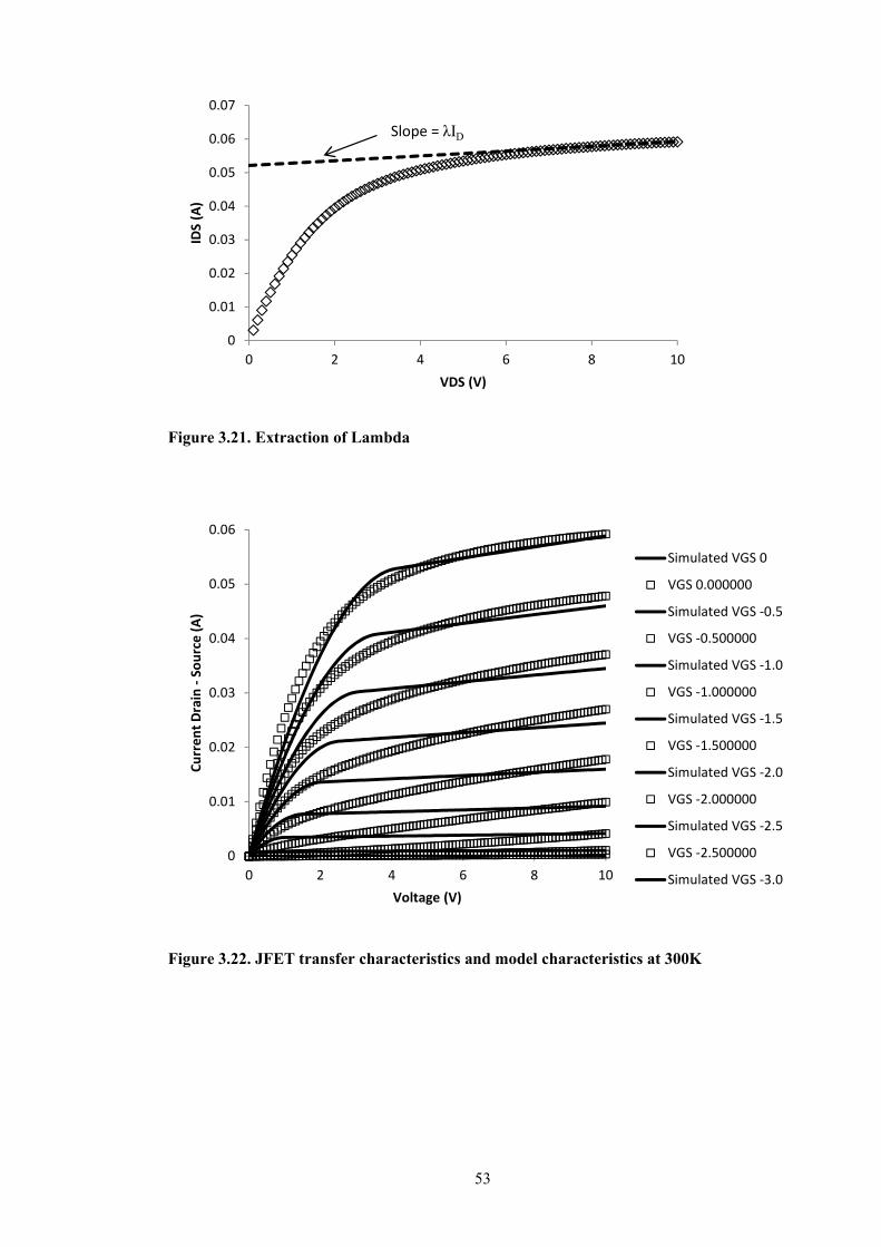
53
Figure 3.21. Extraction of Lambda
Figure 3.22. JFET transfer characteristics and model characteristics at 300K
0
0.01
0.02
0.03
0.04
0.05
0.06
0.07
0 2 4 6 8 10
IDS
(A
)
VDS (V)
Slope = λID
0
0.01
0.02
0.03
0.04
0.05
0.06
0 2 4 6 8 10
Cu
rre
nt
Dra
in -
So
urc
e (
A)
Voltage (V)
Simulated VGS 0
VGS 0.000000
Simulated VGS -0.5
VGS -0.500000
Simulated VGS -1.0
VGS -1.000000
Simulated VGS -1.5
VGS -1.500000
Simulated VGS -2.0
VGS -2.000000
Simulated VGS -2.5
VGS -2.500000
Simulated VGS -3.0
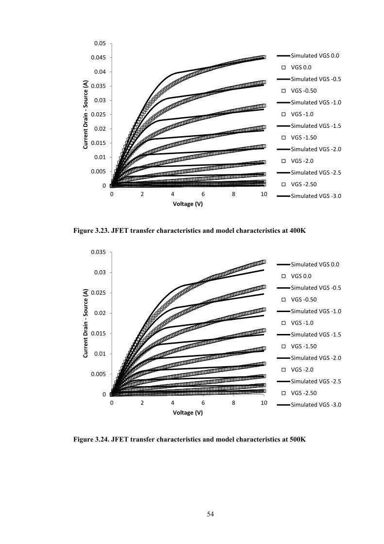
54
Figure 3.23. JFET transfer characteristics and model characteristics at 400K
Figure 3.24. JFET transfer characteristics and model characteristics at 500K
0
0.005
0.01
0.015
0.02
0.025
0.03
0.035
0.04
0.045
0.05
0 2 4 6 8 10
Cu
rre
nt
Dra
in -
So
urc
e (
A)
Voltage (V)
Simulated VGS 0.0
VGS 0.0
Simulated VGS -0.5
VGS -0.50
Simulated VGS -1.0
VGS -1.0
Simulated VGS -1.5
VGS -1.50
Simulated VGS -2.0
VGS -2.0
Simulated VGS -2.5
VGS -2.50
Simulated VGS -3.0
0
0.005
0.01
0.015
0.02
0.025
0.03
0.035
0 2 4 6 8 10
Cu
rre
nt
Dra
in -
So
urc
e (
A)
Voltage (V)
Simulated VGS 0.0
VGS 0.0
Simulated VGS -0.5
VGS -0.50
Simulated VGS -1.0
VGS -1.0
Simulated VGS -1.5
VGS -1.50
Simulated VGS -2.0
VGS -2.0
Simulated VGS -2.5
VGS -2.50
Simulated VGS -3.0

55
Figure 3.25. JFET transfer characteristics and model characteristics at 600K
The models used for the extraction of SPICE parameters as outlined above enable predicted
characteristics to be created using SPICE, which are shown with the experimental data in
figures 3.22 to 3.25. As can be seen from the data in the figures the parameters extracted from
the JFET characteristics used in this work provide models which closely reflect experimental
data.
Whilst there are some discrepancies the variation in electrical characteristics between fabricated
devices primarily due to non-uniformity in doping levels across the wafer and fabrication
repeatability. These models prove sufficient accuracy to model the JFET’s behaviour at various
temperatures.
The parameter values extracted using the models described are summarised in table 3.1.
Temperature (K) Lambda Beta VTO (V) RS Ω CGD CGS
300 0.025 0.0035 -3.99 5.56 24.4 23.2
400 0.029 0.0022 -4.22 4.68 26.0 25.5
500 0.033 0.0011 -4.79 4.39 28.2 27.4
600 0.037 0.0007 -4.93 4.11 30.1 29.8
Table 3.1 Extracted SPICE parameters for silicon carbide JFET structures
0
0.005
0.01
0.015
0.02
0.025
0.03
0.035
0 2 4 6 8 10
Cu
rre
nt
Dra
in -
So
urc
e (
A)
Voltage (V)
Simulated VGS 0.0
VGS 0.0
Simulated VGS -0.5
VGS -0.50
Simulated VGS -1.0
VGS -1.0
Simulated VGS -1.5
VGS -1.50
Simulated VGS -2.0
VGS -2.0
Simulated VGS -2.5
VGS -2.50
Simulated VGS -3.0

56
3.3.3 High Temperature JFET Characteristics
As discussed in chapter 2, the intrinsic properties of silicon carbide allow devices to operate at a
significantly higher temperature than silicon equivalents. The effects of temperature on a typical
device used in this work are discussed in this section. The experimentally extracted data shown
in figure 3.26 is the I-V characteristics of a SiC JFET under zero gate bias conditions. From the
data, it is apparent that increasing temperature significantly reduces the ability of the channel to
conduct current, as is expected from the reduction in carrier mobility with increasing
temperature [14].
Figure 3.26. Zero gate bias characteristics of a SiC JFET with increasing temperature
Figure 3.27. Extracted values of Lambda and Beta as a function of temperature
0
0.01
0.02
0.03
0.04
0.05
0.06
0.07
0 2 4 6 8 10
Cu
rre
nt
(A)
Voltage VDS (V)
300k
400k
500k
600k
0
0.0005
0.001
0.0015
0.002
0.0025
0.003
0.0035
0.004
0
0.005
0.01
0.015
0.02
0.025
0.03
0.035
0.04
300 400 500 600
Be
ta
Lam
bd
a
Temperature (k)
Lambda
Beta
Linear (Lambda)
Poly. (Beta)

57
The data in figure 3.27 shows that the transconductance parameter, β , decreases quadratically
as the temperature increases, indicating a strong dependence on the electron mobility within the
channel. Such closely coupled behaviour reflects the fact that these parameters are dominated by
the carrier mobility behaviour in the channel and suggests that the parameter will also decrease
with increasing ionized carrier concentration as the temperature is increased [15–17]. It can be
seen from the data in figure 3.28, that VTO drops in a linear fashion with increasing temperature
which is related to the decrease in the built in potential of the p-n junction formed by the gate-
channel within the JFET.
The series resistance of the JFET shows an unusual characteristic in that it decreases in a
quadratic manner as the temperature is increased, which is unusual as the bulk resistance of
semiconductors is related to carrier mobility and increases with temperature over the range
studied here [17]. This behaviour is a direct result of both the electrical field and temperature
enhanced trap emission, which cause a decrease in the ionized impurity scattering in the
channel, resulting in a higher carrier mobility and hence lower resistance. This process increases
with temperature until the optical phonon scattering begins to dominate, at which point the
carrier mobility begins to decrease, resulting in an increase in the on-state resistance, similar to
the behaviour observed in a conventional FET [17].
Figure 3.28. Extracted values of VTO and RS as a function of temperature
This anomalous behaviour is only observed in some devices indicating that geometry of the
device might also play a significant role in contributing to this [17], although at this time it is
not possible to uniquely identify the contribution from this source.
y = 2E-05x2 - 0.02x + 10.024
R² = 0.995
-6
-5
-4
-3
-2
-1
0
0
1
2
3
4
5
6
300 400 500 600
VT
O (
v)
Se
rie
s R
esi
sta
nce
(O
hm
s)
Temperature (k)
RS
VTO
Poly. (RS)
Linear (VTO)

58
The data in figure 3.29 shows an increase in gate - source and gate - drain capacitance with
temperature. The origin of these effects is similar to the increase in capacitance observed for
the Schottky diodes discussed in section 3.2. [18].
Figure 3.29. Gate to source capacitance variation with temperature
3.4 High Temperature Passive Components
In order to complement the active devices discussed in the previous section, it is also important
to analyse the effects of elevated temperature on the passive devices required to commission
high temperature electronics. In the circuits described in the following chapters high
temperature capacitors, resistors, and inductors are required and so here their material and
electronic properties will be discussed.
3.4.1 High Temperature Capacitors
High temperature capacitors are arguably the most complex passive component. In this work
Metal Insulator Metal (MIM) capacitors with two different dielectrics Hafnium Dioxide and
Aluminium Nitride have been investigated.
Figure 3.30 depicts the physical structure of the devices with the Hafnium Dioxide capacitors
structure shown on the left and the Aluminium Nitride structure shown on the right.
1E+21
1.2E+21
1.4E+21
1.6E+21
1.8E+21
2E+21
2.2E+21
2.4E+21
2.6E+21
2.8E+21
0 0.5 1 1.5 2
1/C
2
Reverse bias Voltage (V)
300k
325k
350k
375k
400k
425k
450k
475k
500k
525k
550k
575k
600k
625k

59
Figure 3.30. Physical Structure of High Temperature MIM capacitors
Hafnium dioxide is a high-κ dielectric which allows the realisation of physically thicker
dielectric layers in comparison to conventional SiO2 based capacitor structures, such as those
found in MOSFETs, whilst maintaining a high capacitance. Reports in the literature have
demonstrated the compatibility of HfO2 capacitors for use in high dose radioactive and high
temperature environments [18, 19]. The capacitors used in this work had a physical thickness of
60nm and were built with the intention of integrating the capacitors on the surface of the active
semiconductor devices, to enable a system on chip (SOC) solution to circuit development.
The data in figure 3.31 shows a comparison of the I-V characteristics of a typical “Good” and
“Bad” HfO2 MIM capacitor. The observed increase in leakage current of the “Bad” capacitor is
around five orders of magnitude and is due partly to the increased area in comparison to the
“Good” device, but also shows evidence of additional leakage mechanisms. Testing on a large
number of devices indicated that this additional leakage was observed in all large area devices,
as well as a significant fraction of the small area devices, suggesting that the mechanism is
linked to a high concentration of defects in the dielectric, which limits the yield. Additionally, it
can be seen that even the good devices exhibit a leakage current in the nA range at a bias of 5V,
which will result in problems when deployed in the electrical circuits presented later in this
thesis.
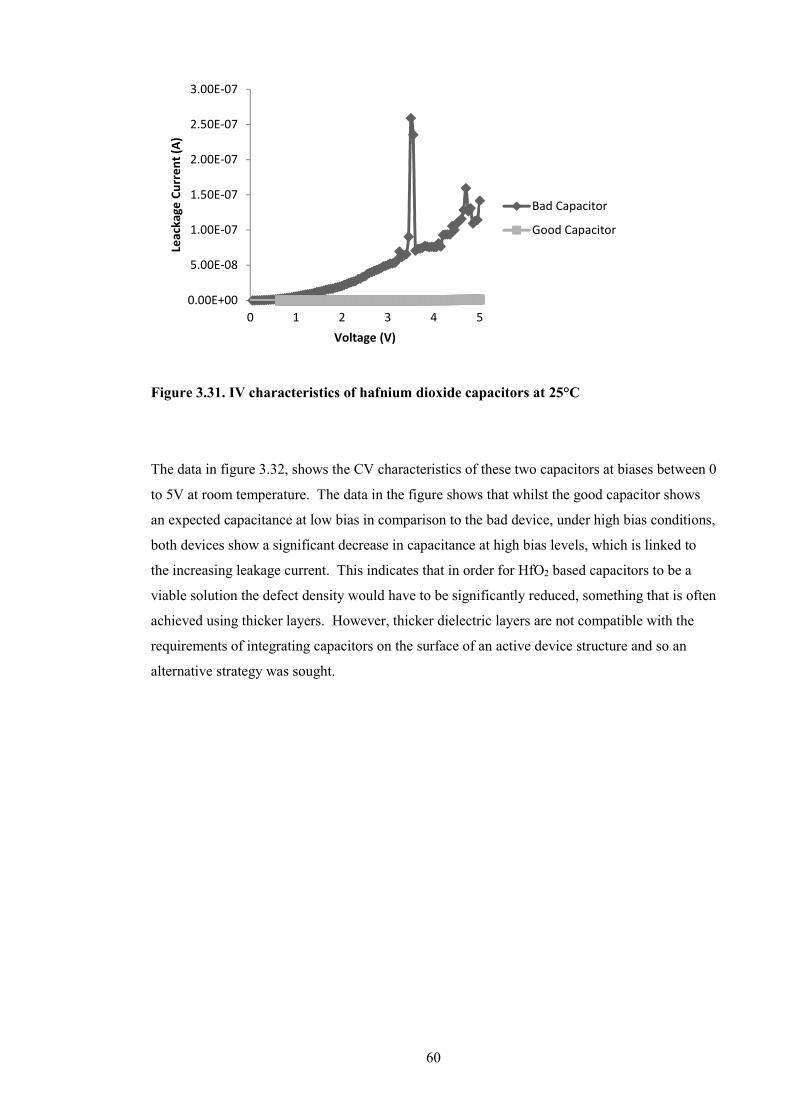
60
Figure 3.31. IV characteristics of hafnium dioxide capacitors at 25°C
The data in figure 3.32, shows the CV characteristics of these two capacitors at biases between 0
to 5V at room temperature. The data in the figure shows that whilst the good capacitor shows
an expected capacitance at low bias in comparison to the bad device, under high bias conditions,
both devices show a significant decrease in capacitance at high bias levels, which is linked to
the increasing leakage current. This indicates that in order for HfO2 based capacitors to be a
viable solution the defect density would have to be significantly reduced, something that is often
achieved using thicker layers. However, thicker dielectric layers are not compatible with the
requirements of integrating capacitors on the surface of an active device structure and so an
alternative strategy was sought.
0.00E+00
5.00E-08
1.00E-07
1.50E-07
2.00E-07
2.50E-07
3.00E-07
0 1 2 3 4 5
Lea
cka
ge
Cu
rre
nt
(A)
Voltage (V)
Bad Capacitor
Good Capacitor

61
Figure 3.32. CV measurements of Hafnium Dioxide Capacitors
The realisation of hybrid circuits in high temperature electronics utilises discrete devices, both
active and passive, being integrated onto a high temperature ceramic circuit board, which is
often fabricated from aluminium nitride (AlN). For this reason, an investigation into the
suitability of AlN dielectrics for high temperature capacitors has been undertaken. The structure
of a typical Aluminium Nitride capacitor is shown in figure 3.30.b and shows a marked
difference in comparison to the HfO2 device studied previously, in so much that the physical
thickness of the AlN dielectric film has been increased to 390nm. The data in figure 3.33 shows
the current voltage characteristics of a typical AlN capacitor. It can be seen from the data that
in order to induce leakage currents of a magnitude similar to those observed in the HfO2 devices
the AlN MIM capacitors requires the application of a bias voltage of 15V at a temperature of
600K, and measurements have had to be made at increased temperature. These characteristics
have been chosen to highlight the superior leakage current exhibited by AlN capacitors at over
the temperature range studied, indicating their suitability for deployment in electronic circuits
operating at elevated temperatures.
1.93E-11
1.93E-11
1.94E-11
1.94E-11
1.95E-11
1.95E-11
1.96E-11
1.96E-11
1.97E-11
1.97E-11
1.98E-11
1.74E-10
1.74E-10
1.75E-10
1.75E-10
1.75E-10
1.75E-10
1.75E-10
1.76E-10
1.76E-10
0 1 2 3 4 5
"Go
od
" C
ap
aci
tor
cap
aci
tan
ce (
F)
"Ba
d"
cap
aci
tor
cap
aci
tan
ce (
F)
Voltage (V)
"Bad" Capacitor
"Good" capacitor

62
Figure 3.33. I-V Characteristics of Aluminium Nitride Capacitors
The CV characteristics of a typical AlN capacitor are shown by the data in figure 3.34. The data
shows a low voltage dependence of the measured capacitance in comparison to that observed in
the HfO2 data in figure 3.32, which is consistent with the low leakage currents observed in the
AlN structures. This constant capacitance behaviour is a key factor in the design of high
performance analogue circuits, because it removes the need to maintain the bias level on the
capacitor at a standard value, simplifying the circuit design. The data in the figure also shows
that the zero bias capacitance increases by over 10% as the temperature rises from 300 to 650K.
The data in figure 3.35 shows the variation in zero bias capacitance as a function of temperature
and it can be observed that the increase is linear with temperature and this is an important
feature which must be considered when designing high temperature circuits. This challenge in
circuit design will be discussed further in the upcoming chapters.
-7.0E-08
-5.0E-08
-3.0E-08
-1.0E-08
1.0E-08
3.0E-08
5.0E-08
7.0E-08
-15 -10 -5 0 5 10 15
Lea
ka
ge
Cu
rre
nt
(A)
Voltage Bias (V)
525k
550k
575k
600k

63
Figure 3.34. CV characteristics of AlN capacitor with increasing temperature
Figure 3.35. Linear temperature coefficient of a typical AlN capacitor
106
108
110
112
114
116
118
120
122
-5 -3 -1 1 3 5
Ca
pa
cita
nce
(p
F)
Bias Voltage (V)
Increasing
Temperature
y = 0.0434x + 93.593R² = 0.9911
104
106
108
110
112
114
116
118
120
122
300 350 400 450 500 550 600
Avera
ge C
apacitance (
pF
)
Temperature K

64
3.4.2 High Temperature Resistors
Resistors, inductors and track resistance are important passive components to consider for high
temperature circuits. They share a common theme for high temperature usage as they are often
based on thin film technologies, which employ a thin metallic layer. In contrast to high
temperature capacitors, which are an area of active research, the simpler structure and materials
challenges, reliable high temperature resistors are already commercially available [20].
In this work commercially available resistors from Rhopoint components which were rated for
up to 300°C were characterised and used in high temperature hybrid circuits. [20]. Sample
devices were heated to 400°C and their electrical resistance characterised to extract the
temperature co-efficient for use in circuit simulation.
Figure 3.36 – Resistance as a function of temperature for samples of high temperature
resistors used.
The data in figure 3.36 depicts the variation in resistance of these commercially available high
temperature resistors at temperatures up to 375°C From the data, it is apparent that that the
resistor rated at 1KΩ exhibits a positive temperature co-efficient whereas the 100KΩ resistor
exhibits a negative temperature co-efficient over the temperature range studied. This difference
is most likely due to different materials being utilised to achieve the different resistance values
whilst being of a standard physical dimension.
996
998
1000
1002
1004
1006
1008
1010
1012
1014
95500
96000
96500
97000
97500
98000
98500
99000
99500
100000
25 75 125 175 225 275 325 375
Re
sist
an
ce (
10
0K
) (O
hm
s)
Temperature (Degrees)
100K Resistor
1K Resistor

65
Figure 3.37. Extracted temperature co-efficient for 1KΩ commercial resistor
Figure 3.38. Extracted temperature co-efficient for 100KΩ commercial resistor
The change in resistance with temperature is described using polynomial equations, as shown
by the lines of best fit in figures 3.37 and 3.38. This enabled the resistance variation to be
described in SPICE based circuit simulations.
3.5 Properties of metals at High Temperature
At elevated temperatures it is important to utilise metals which are chemically stable and do not
react with chemicals present in the environment in which they are to be employed. These
metals must also not undergo solid state chemical reactions or suffer significant diffusion with
y = 4E-07x3 - 0.0007x2 + 0.4259x + 923.66
R² = 0.9933
996
998
1000
1002
1004
1006
1008
1010
1012
1014
300 350 400 450 500 550 600 650
Re
sist
an
ce (
Oh
ms)
Temperature (K)
y = -8E-05x3 + 0.0999x2 - 44.947x + 106451
R² = 0.9981
95500
96000
96500
97000
97500
98000
98500
99000
99500
100000
300 350 400 450 500 550 600 650
Re
sist
an
ce (
Oh
ms)
Temperature (K)

66
other material present in the electronic circuit, such as ceramic circuit boards and wire bonds.
Standard electrochemically deposited copper, which is used in standard silicon electronic circuit
boards oxidises and is unsuitable for use in high temperature environments [21]. Hence, it is
preferable to use a non reactive metal with a high electrical conductivity and so in this work
gold was selected. This selection was also based on the availability of process techniques and
knowledge within the research group, including the suitability of titanium as an adhesion
promoting diffusion layer underneath the gold film. It is possible to plate a layer of gold on to
existing copper to prevent oxidation or alternatively for higher temperatures it is common to use
electroplated gold traces, as has been used in this work.
The resistance of a gold track can be calculated using the standard formula for a bulk conductor
(i.e. where the cross sectional area is such that the surface roughness scattering is insignificant)
LR
A
ρ= 3.37
The bulk resistivity of metals changes with temperature and when designing high temperature
circuits more attention must be paid to the temperature coefficient. For simulation purposes, the
resistivity of the metal can be calculated at different temperatures
( )1ref refT Tρ ρ α = + − 3.38
Where ρ is the resistance at the temperature of interest, refρ the resistivity at the reference
temperature, α the Temperature coefficient for the metal, T the temperature of the metal, and
refT the reference temperature for which α is specified [21]. From these equations it is
possible to calculate the resistances of traces and the additional contribution to the resistance
resulting from the elevated temperature.
3.6 High temperature magnetic components
Planar spiral inductors have been used to fabricate low inductance devices such as those
required for RF circuits, with ferrite cores used for the transformers required for power
converters. For both inductor types considered here, the challenge of keeping the resistance of
the conducting track as low as possible is important for minimising power loss and Q factor
degradation, this ensuring their optimum operation.

67
3.6.1 High Temperature Spiral Inductors
For low values of inductance it is possible to create inductors by fabricating a planar spiral
structure on a ceramic substrate. Gold spiral inductors were fabricated using conventional
photolithography techniques, followed by gold electroplating to reduce their resistance. The
literature contains details of models describing the characteristics of planar inductors, however
for the devices considered in this work a simple calculation sufficed, due to both the physical
size of the inductors and the limitations in the processing technology used.
The inductance of a planar spiral conductor on an insulating substrate can be described using
( )
( )
2
2
30 112
i
i
i
D N W SN
LD N W S
D
+ + =+ +
−
3.39
Where L is the predicted inductance, iD is the inner diameter of the inductor, N is the
number of turns, W the wire diameter, and S the spacing between the turns.
After deposition by ebeam evaporation, the titanium and gold seed layers were patterned using
conventional photolithography and were then electroplated to increase their physical thickness
and reduce their resistance to improve their performance as inductors. After electroplating, the
characteristics were extracted as a function of temperature to enable the simulation of circuits.
As shown by the data in figure 3.39 the DC resistance of the inductor increases linearly with
temperature, as is expected from the behaviour of the bulk resistivity. It is important to note that
the resistance of this inductor increases by nearly a factor of three over the temperature range
studied and this observation highlights the importance of selecting appropriate conductors for
high temperature circuits. The data in figure 3.40 shows the inductance of a typical gold spiral
inductor over a range of temperatures as a function of measurement frequency. It is apparent
from the data that the increasing temperature causes a small increase in inductance, which is
most likely due to the properties of the ceramic substrate on which the inductor was fabricated.
As the material properties of the substrate alter as does the capacitance between tracks of the
inductor along with the inductor shape changing due to thermal expansion.

68
Figure 3.39. – DC resistance of gold inductor at elevated temperatures
It is also apparent that inductance is higher at lower frequencies which is to be expected and
even at DC the range of experimentally measured inductance values corresponds well to the
theoretical value calculated by equation 3.39 of 1.25µH.
Figure 3.40. Measured inductance values for a gold spiral inductor
0
1
2
3
4
5
6
300 350 400 450 500 550 600 650
DC
re
sist
an
ce (
Ω)
Temperature (k)
1.244E-06
1.246E-06
1.248E-06
1.25E-06
1.252E-06
1.254E-06
1.256E-06
1.258E-06
1.26E-06
1.262E-06
1.264E-06
0 500000 1000000 1500000 2000000
Ind
uct
an
ce (
H)
Frequency (Hz)
300k
325k
350k
375k
400k
425k
450k
475k
500k
525k
550k
575k
600k
625k
650k

69
3.7 Conclusions
This chapter has discussed the characterisation and extraction of SPICE parameters for use in
models when designing high temperature circuits made from SiC components and proprietary
high temperature passive components. The extracted SPICE parameters were using in circuit
simulation software to aid in the development of SiC circuits in later chapters.
JFETs were characterised at temperatures up to 573K, and values for TOV ,β , λ , IS , RS and
junction capacitances were extracted and then used to mathematically describe the operation of
circuits using SPICE. The transconductance of SiC JFETs has been shown to decrease
quadratically with temperature indicating a strong dependence upon carrier mobility in the
channel. The channel resistance also decreased quadratically as a direct result of both electric
field and temperature enhanced trap emission. The JFETs were tested to be operational up to
775K, where they failed due to delamination of an external passivation layer.
Schottky diodes were characterised up to 573K, across the temperature range and values for
ideality factor, capacitance, series resistance and forward voltage drop were extracted to
mathematically model the devices. The series resistance of a SiC SBD exhibited a quadratic
relationship with temperature similar to that observed in the JFET indicating that it is dominated
by optical phonon scattering. The observed deviation from a temperature independent ideality
factor is due to the recombination of carriers in the depletion region affected by both traps and
the formation of an interfacial layer at the SiC/metal interface.
To compliment the silicon carbide active devices utilised in this work, high temperature passive
devices and packaging/circuit boards were developed. Both HfO2 and AlN materials were
investigated for use as potential high temperature capacitor dielectrics in metal-insulator-metal
(MIM) capacitor structures. The different thicknesses of HfO2 (60nm and 90nm) and 300nm for
AlN and the relevance to fabrication techniques are examined and their effective capacitor
behaviour at high temperature explored. The HfO2 based capacitor structures exhibited high
levels of leakage current at temperatures above 100°C and moderate electric fields due to the
thin dielectric and high defect density rendering the unsuitable as capacitors in hostile
environments. To address this issue AlN capacitors with a greater dielectric film thickness were
fabricated with reduced leakage currents in comparison even at an electric field of 50MV/cm at
600K.
Commercial thick film metal oxide resistors were characterised up to 648K. Resistors with a
lower resistance value exhibited a positive temperature co-efficient whereas higher valued

70
resistors exhibited a negative temperature co-efficient. This difference is most likely due to
different materials being utilised to achieve the different resistance values whilst being of a
standard physical dimension. The drift of resistance with temperature must be considered when
applied to high temperature circuits as it results in change of current levels.
Finally the properties of metals at elevated temperature were considered with regards to both
PCB traces and spiral inductors. Gold was selected as the most appropriate metal to be used for
interconnects and RF spiral inductors as it is chemically stable and would not react with
chemicals present in hostile environments. RF spiral inductors were fabricated by
electrochemical deposition before being characterised at high temperature, the inductance and
resistance values agree closely with theoretical formula over the entire temperature range.
3.8 References
[1] Milton Bergstein, Studies in contact rectification I. Classification of contact rectifiers. Paper
presented at the Fifty-seventh General Meeting of the American Electrochemical Society, held
at St. Louis, Mo. May 30, 1930
[2] Konstantin Vassilevski et al, Silicon Carbide Vertical JFET Operating at High Temperature,
Materials Science Forum Vols. 600-603 (2009) pp 1063-1066
[3] Mustafa G. Guvench, SPICE Parameter Extraction From Automated Measurement Of JFET
and MOSFET Characteristics In The Computer-Integrated Electronics Laboratory, Proceedings
of A.S.E.E, Session 1659, 1994.
[4] Ming Hung Weng et al, Comparison of Parameter Extraction Techniques for SiC Schottky
Diodes. MRS Proceedings, 911, 0911-B10-12 doi:10.1557/PROC-0911-B10-12.
[5] Yi Wang et al, SPICE Model of SiC JFETs for Circuit Simulations, IEEE COMPEL
Workshop July 2006.
[6] T. R. McNutt et al, Parameter Extraction Sequence for Silicon Carbide Schottky, Merged
PiN Schottky, and PiN Power Diode Models, National Science Foundation Grant #ECS-011553
[7] C. Raynaud et al, Barrier height determination of SiC Schottky diodes by capacitance and
current–voltage measurements, J. Appl. Phys. 91 , 9841 (2002)
[8] B. J. Skromme et al, Electrical Characteristics of Schottky Barriers on 4H-SiC: The Effects
of Barrier Height Non-uniformity J. Electronic Materials, Vol. 29, No. 3, 2000.

71
[9] Adrian Powell, Three inch silicon carbide wafer with low warp, bow, and TTV, Patent US
7422634 B"
[10] K. Vassilevski et al, High Voltage Silicon Carbide Schottky Diodes with Single Zone
Junction Termination Extension, Materials Science Forum Vols. 556-557 (2007) pp. 873-876
[11] Rhoderick, Emlyn Huw, and R. H. Williams. "Metal-semiconductor contacts." (1988).
[12] Physics of Semiconductor Devices, Simon M. Sze, Kwok K. Ng
[13] Harold Shichman, David A. Hodges, Modeling and Simulation of Insulated-Gate Field-
Effect Transistor Switching Circuits, IEEE JOURNAL OF SOLID-STATE CIRCUITS,
September 1968
[14] J E Lees et al, SiC X-ray detectors for harsh environments, Journal of Instrumentation, Vol.
6, Jan 2011.
[15] Elisa Platania, A Physics-Based Model for a SiC JFET Accounting for Electric-Field-
Dependent Mobility, IEEE Transactions on Industry applications, Vol. 47, No. 1 Jan/Feb 2011.
[16] C. J. Scozzie et al, Modelling the temperature response of 4H silicon carbide junction field,
J. Appl. Phys. 81 (11), 1 June 1997
[17] P. Bhatnagar et al, High Temperature Characterisation of 4H-SiC VJFET, Materials
Science Forum Vols. 556-557 (2007), pp. 799-802.
[18] Simon Barker et al, Silicon Carbide Based Energy Harvesting Module for Hostile
Environments, 2010, Materials Science Forum, 645-648, 1093
[19] Bing Miao, Radiation Induced Change in Defect Density in HfO2 Based MIM Capacitors,
IEEE Transactions on Nuclear Science, 2009
[20] Rhopoint, High Temperature Chip Resistors, Datasheet
[21] High Temperature Electronics, Randall Kirschman, IEEE Press
[22] J. G. Macgregor, On the Variation with Temperature of the Electrical Resistance of Wires
of certain Alloys, Transactions of the Royal Society of Edinburgh, Vol. 29, Jan 1880.

72
Chapter 4: Silicon Carbide Electronic Oscillators
4.1 Introduction
A significant number of electronic circuits have the requirement to produce repetitive
waveforms to perform multiple functions. In order to meet this requirement oscillator circuits
have been realised, which depending on complexity can produce any waveform including high
frequency radio waves. These carrier signals are often utilised as the basis of wireless
communication systems.
This chapter provides an overview of different oscillator types, before focusing on Colpitts
Oscillators for use within a high temperature prototype communication circuit. The origin of the
observed frequency drift with temperature of these oscillators fabricated using Silicon Carbide
components is explored. A development of this circuit has been used to demonstrate a silicon
carbide Colpitts based Voltage Controlled Oscillator (VCO) and the data shows that this is
suitable as a method of controlling the frequency of an oscillator across a range of temperatures.
The data in this chapter shows, for the first time, both Amplitude modulation (AM) and
Frequency modulation (FM) of high temperature circuits producing carrier waves and the
realisation of a high temperature wireless communication system.
4.2 Experimental
4.2.1 The Electronic Oscillator
An electronic oscillator is a circuit which produces a repetitive, oscillating signal by converting
a direct current (DC) power supply to an alternating current (AC) signal. The shape of the signal
waveform depends on the application for which the oscillator is designed, for example clock
generation for digital electronics, switching waveforms for switch mode power supplies, and
radio frequency signals for wireless electronic communications.
Electronic oscillators can be described as two main types: the nonlinear oscillator and the linear
or harmonic oscillator.
4.2.2 The nonlinear oscillator
The nonlinear or relaxation oscillator produces a non sinusoidal waveform, such as a square
wave, sawtooth or triangle waveform. The circuit comprises an energy storage component,

73
along with a nonlinear switching circuit. In the majority of implementations this is in the form
of a capacitor, however inductors can also be used. Alternative implementations include a
negative resistance device that periodically charges and discharges the energy in the storage
element, thus causing abrupt changes in the output waveform. Square wave relaxation
oscillators are used extensively in digital electronics to provide the clock signal for sequential
logic circuits such as timers and counters, whereas sawtooth oscillators are used specifically in
time base circuits. [1-3]
4.3 Linear oscillators
The linear or harmonic oscillator produces a sinusoidal waveform. Two types of linear oscillator
are possible the negative resistance oscillator and the feedback oscillator.
4.3.1 Negative resistance oscillators
The negative resistance oscillator is based around a component which exhibits negative
resistance, such as a magnetron tube, or certain types of diode. In silicon carbide technology
impact ionization avalanche transit-time (IMPATT) diodes have been experimentally
demonstrated which will enable the practical realisation of this type of oscillator [5, 6].
To explain the operation of these oscillators it is important to understand the concept of negative
resistance. The simple tank circuit, shown in figure 4.5 (a), is stimulated by a current impulse
applied at inI . The tank responds with a decaying oscillatory behaviour because, in every cycle,
some of the energy that reciprocates between the capacitor and inductor is lost as heat in the
resistor, pR . If a device or circuit which exhibits negative resistance is placed in parallel with
pR it can be modelled as pR− . If the magnitude of this negative differential resistance
pR− , is
equal to the tank losses the oscillations observed in Vout continue indefinitely, as shown in figure
4.5.(b) and the circuit can be described as an oscillator.

74
Figure 4.5 (a) Decaying impulse response of a tank circuit, (b) addition of negative
resistance to cancel the power loss in Rp. [7]
Such oscillators are commonly used in the production of high frequencies, such as those found
in the microwave region and above. The advantage of silicon carbide in these circuits is the high
saturation velocity of electrons ( )7 12 10SATv cms−= × in comparison to commonly used
semiconductors such as silicon ( )7 11 10SATv cms−= × , enabling higher frequency operation
and the capability to operate at higher temperatures thus allowing designers to dissipate much
higher power levels in the devices. [8]
Figure 4.6 (a) Circuit of an IMPATT diode based negative resistance oscillator (b)
Schematic representation of an IMPATT diode
The circuit diagram in Figure 4.6(a) schematically depicts a negative resistance oscillator circuit
based on an IMPATT diode. This example is based on the use of an LC circuit, (alternative
schematics based on the use of a crystal or cavity resonator are possible) which is connected

75
across an IMPATT diode which exhibits a negative differential resistance and a DC bias voltage
supplies the energy required to sustain the oscillations. As shown by the waveform in figure
4.5(a) a resonant circuit acts in a manner similar to that of an oscillator in that it has the ability
to store energy in the form of electrical oscillations if excited. However the existence of internal
resistance acts to damp the oscillations and the amplitude decreases to zero. The negative
resistance of the active device cancels the internal resistance in the resonator, thus creating a
resonator with no damping, which creates continuous oscillations at the resonant frequency
predicted using equation 4.5.
4.3.2 The feedback oscillator
The feedback oscillator is the most common form of linear oscillator as shown in figure 4.7. It
requires the use of an active component, an electronic amplifier such as a transistor, connected
in a feedback loop, with its output fed back into its input through a frequency selective
electronic filter in order to provide positive feedback.
Figure 4.7 Schematic representation of feedback oscillator
When power is first supplied to the amplifier, the electronic noise in the circuit provides the
initial signal to initiate the oscillations. The magnitude of the noise is increased by means of the
amplification in the feedback loop, before the desired frequency is selected by the filter, until
the signal becomes a sine wave.
Feedback oscillator circuits can be classified according to the type of frequency selective filter
employed in the feedback loop. There are three specific types; crystal oscillators, RC oscillators,
and LC oscillators each with their own merits and limitations.
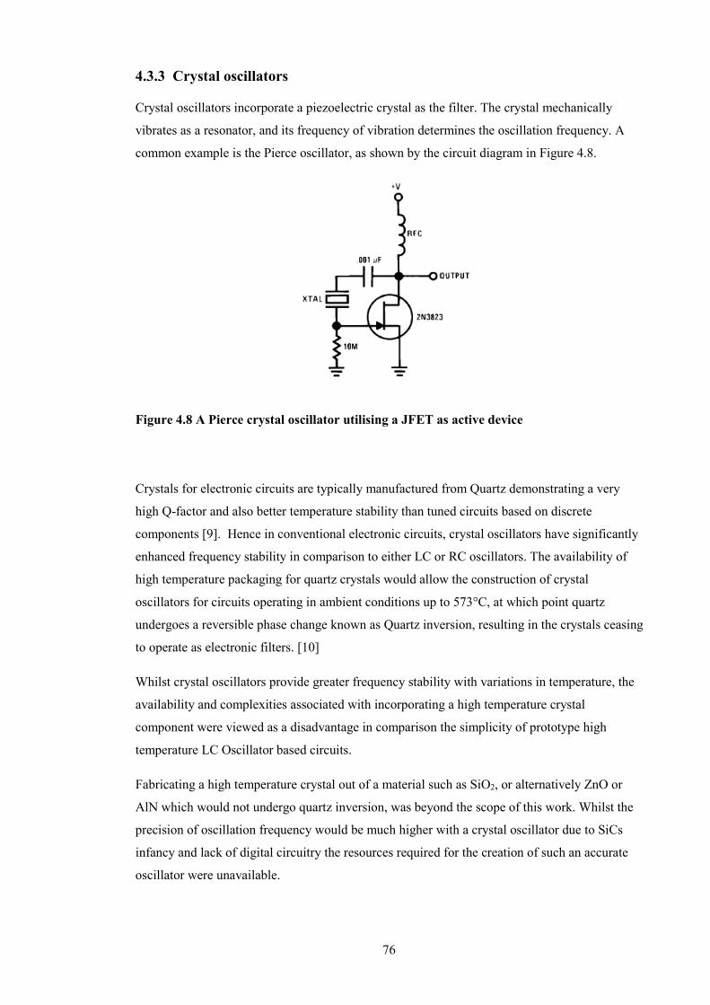
76
4.3.3 Crystal oscillators
Crystal oscillators incorporate a piezoelectric crystal as the filter. The crystal mechanically
vibrates as a resonator, and its frequency of vibration determines the oscillation frequency. A
common example is the Pierce oscillator, as shown by the circuit diagram in Figure 4.8.
Figure 4.8 A Pierce crystal oscillator utilising a JFET as active device
Crystals for electronic circuits are typically manufactured from Quartz demonstrating a very
high Q-factor and also better temperature stability than tuned circuits based on discrete
components [9]. Hence in conventional electronic circuits, crystal oscillators have significantly
enhanced frequency stability in comparison to either LC or RC oscillators. The availability of
high temperature packaging for quartz crystals would allow the construction of crystal
oscillators for circuits operating in ambient conditions up to 573°C, at which point quartz
undergoes a reversible phase change known as Quartz inversion, resulting in the crystals ceasing
to operate as electronic filters. [10]
Whilst crystal oscillators provide greater frequency stability with variations in temperature, the
availability and complexities associated with incorporating a high temperature crystal
component were viewed as a disadvantage in comparison the simplicity of prototype high
temperature LC Oscillator based circuits.
Fabricating a high temperature crystal out of a material such as SiO2, or alternatively ZnO or
AlN which would not undergo quartz inversion, was beyond the scope of this work. Whilst the
precision of oscillation frequency would be much higher with a crystal oscillator due to SiCs
infancy and lack of digital circuitry the resources required for the creation of such an accurate
oscillator were unavailable.

77
4.3.4 RC Oscillators
RC oscillators utilise a filter network comprising combinations of resistors and capacitors and
are commonly used to produce lower frequencies, such as those in the kHz frequency range. A
common example of an RC oscillator is the phase shift oscillator shown in figure 4.9.
Figure 4.9 Phase shift oscillator utilising a JFET [7]
In this circuit topology, it can be seen that the JFET is operating as an inverting amplifier
producing a signal which is 180° phase shifted from the signal at the input. The RC phase shift
network acts as a filter and provides an identical 180° phase shift by using three RC sections in
cascade, each producing a 60° phase shift. In the majority of examples the capacitors and
resistors share common values and excluding parasitics from the circuit layout, the frequency of
oscillation can be determined using
1
2 6f
RCπ= 4.4
4.3.5 LC Oscillators
In an LC oscillator, the filter is a tuned circuit commonly referred to as a tank circuit, which
consists of an inductor and a capacitor connected together. During operation, charge flows back
and forth between the capacitors plates through the inductor, allowing the tuned circuit to store
energy at the resonant frequency.
This oscillating transfer of energy takes place at a frequency determined by the capacitance and
inductance values, known as the resonant frequency and can be calculated using:

78
0
1
2f
LCπ= 4.5
where L is the inductance and C the capacitance.
This resonant frequency is generally expressed in the resonant angular frequency form.
1
LCω = 4.6
As discussed in the previous sections, internal losses exist within the tank circuit, however the
amplifier compensates for these losses and supplies power for the output signal, maintaining the
amplitude of the oscillations. LC oscillators are commonly used at radio frequencies and when
a tuneable frequency source is required, typical circuit configurations are the Hartley, Colpitts
and Clapp oscillators, as shown by the circuit topologies in Figures 4.10 (a), (b) and (c)
respectively.
Figure 4.10 (a) Hartley, (b) Colpitts and (c) Clapp oscillators
As can be seen from the schematic circuit layout in figure 4.10 the Colpitts and Clapp
Oscillators lend themselves to a greater level of miniaturisation than the Hartley oscillator, as
they only utilise a single inductor in the design. In this work a Colpitts oscillator design was
selected due to their ability to self start utilising components with a lower quality factor (Q
value) than the slightly more complicated Clapp design.

79
4.3.6 The Colpitts Oscillator
The Colpitts oscillator, shown in figure 4.10(b) is a common form of LC oscillator utilising a
LC tank circuit and an active device to counter act the damping effect caused by the parasitic
resistances which exist within all components. A Colpitts oscillator can be realised using a
single silicon carbide JFET as an amplifier and by adding a tank circuit. By feeding the signal
back from the output of the amplifier to the input through this LC tank it is possible to create a
practical Colpitts oscillator circuit, as shown schematically in fig 4.11
Figure 4.11 Circuit schematic of a Colpitts Oscillator
As described in the literature, a linear systems feedback approach is commonly used for the
analysis of a Colpitts Oscillator [11]. This approach enables the determination of the oscillator
frequency ( 0f ) and the minimum transconductance ( mg ) required by the JFET to enable steady
state oscillations, as shown by equations 4.7 and 4.8 respectively.
0
1 2
1 2
1
2
fC C
LC C
π
=
+
4.7
2
1
m o
Cg r
C= 4.8
Where the terms in the equation are denoted by the labels in figure 4.11.
The frequency of oscillation calculated using this closed loop analytical approach results in
higher frequencies than those predicted using either SPICE based simulations (using the
parameters discussed in chapter 3) and experimental results, because these formulae do not
consider the impact of the parasitic capacitances within the JFET and/or the capacitances caused
by the wirebonds which are difficult to calculate and depend upon circuit design and chip
placement. The parasitic capacitances however are of magnitudes smaller than the size of the
capacitors used in the circuits which in some calculations allows them to be omitted. It is also

80
possible to use an alternative approach based on the concept of negative resistance [13] in one-
port oscillators such as the silicon carbide IMPATT diode, replacing the silicon carbide JFET
with an external oscillator active circuit.
Fig 4.12 RLC tank with negative resistance created by the Oscillator active network
A schematic of a circuit layout for this concept is shown in fig 4.12. It can be see that in order
to overcome the energy loss from the parasitic resistance in the circuit components including the
inductor, the active circuit must form a small-signal negative resistance negR , which replenishes
the energy loss during every oscillation cycle. Thus the negative resistance can be interpreted as
a source of energy. In this example pR denotes the equivalent parallel resistance of the tank and
for oscillations to be self-starting it is necessary that neg pR R> . As the amplitude of the
oscillations increases, the amplifier will start to saturate, decreasing the loop gain until it reaches
unity, thereby satisfying the Barkhausen criterion [14]. The Barkhausen stability criterion is a
mathematical condition put forth in 1921 by German physicist Heinrich Georg Barkhausen to
determine when a linear electronic circuit will oscillate. In the steady state the two resistances
must be of equal amplitude and so the power drawn from the source balances that lost in the
parasitic resistance.
This more considered analytical approach allows for the inclusion of the parasitic capacitance of
the JFET, thus yielding a predicted oscillation frequency which is a closer match to the
experimentally observed value. A simplification of the circuit shown in figure 4.11, by ignoring
the contribution from the inductor (L), an ac equivalent circuit can be derived, as shown in fig.
4.11 and this can be used to calculate the input impedance of the circuit.

81
Figure 4.13. An ac equivalent circuit of a Colpitts oscillator structure highlighting the
parasitic capacitances in the JFET but ignoring the inductor
In figure 4.13 the parasitic capacitances of the JFET (denoted as Q) have been included to
represent the depletion capacitance of the gate channel junction; gate-source (gsC ) and gate-
drain (gdC ) capacitances; as well as the drain-source ( dsC ) capacitance resulting from the
physical dimensions of the charge storage in the channel.
( )2
1s
ds
Zj C Cω +
≫ 4.10
( )2
1ds
ds
rj C Cω +
≫ 4.11
( )1
1gs
gs
rj C Cω +
≫ 4.12
Where dsr and gsr are the small-signal drain-source and gate-source resistances of the JFET
respectively.
Providing the conditions stipulated in equations 4.10 to 4.12 are met, it is possible to replace the
SiC JFET, with a simplified small signal model, to obtain the equivalent circuit shown in fig.
4.14, where mg is the small-signal transconductance of the SiC JFET.

82
Figure 4.14 Small-signal equivalent of the Colpitts Oscillator
Utilising standard circuit theory and the methods in the literature, [13] it is possible to determine
the negative differential resistance required to sustain oscillations in the circuit, based on the
topology shown in figure 4.14;
( )( )21 2
1 2
1
mneg
gd gd
gs ds
gs ds
gr
C CC C C C
C C C Cω
= −
+ + + + + +
4.13
A total capacitance of the circuit can be defined using
( ) ( )1 2
1 2 1 2
1gs ds gd gd
t
gs ds gs ds
C C C C C CC
C C C C C C C C
+ + = + + + + + + +
4.14
and so, combining this with equation (2.7), the commonly expressed equation for the
differential resistance can be obtained [4, 11]:
21 2
mneg
gr
C Cω= − 4.15
Based on this analysis and reinstating the inductor to the circuit, along with a series total loss
resistance, tR , to the input impedance inZ , it is possible to obtain a simplified series equivalent
circuit of the Colpitts oscillator, as shown in fig. 4.15.

83
Figure 4.15 Series equivalent circuit of the Colpitts Oscillator
Where tr is the total series loss resistance and can be calculated from the series resistance of the
capacitors and inductors using:
1 2t L C Cr r r r= + + 4.16
Hence, the equivalent parallel resistance of the Colpitts oscillator, tank circuit pR can be
expressed as:
( )( )1 2
1 2 1 2
1
p
gs ds gd gd
t
gs ds gs ds
LR
C C C C C Cr
C C C C C C C C
=+ +
+ + + + + + +
4.17
By substituting in equation 4.14 into equation 2.7, the oscillation frequency is found to be
( )( )1
1 22
1 2 1 2
1gs ds gd gd
gs ds gs ds
C C C C C CL
C C C C C C C Cω
− + + = + + + + + + +
4.18
Frequency in Hertz can therefore be given by:
( )( )1
1 2
1 2 1 2
0
1
2
gs gs gd gd
gs ds gs ds
C C C C C CL
C C C C C C C Cf
π
− + + + + + + + + + = 4.19
Substituting equation 4.18 into 4.13 yields:
1 2
mL
neg
gs ds
gr
C C C C= −
+ + + 4.20
Finally referring back to figure 4.14, it is possible to determine the start-up conditions for this
Colpitts oscillator in terms of negative resistance as:

84
( )
( )( )
2
1 2
1 2
1 2
1
gs ds
neg
gd gd
m gs ds
gs ds
C C C CR
C Cg C C C C
C C C C
+ + += −
+ + + + + +
4.21
4.4 High Temperature Colpitts Oscillator
To demonstrate the accuracy of the model detailed in section 4.2 for determining the frequency
of an oscillator, a comparison between the predicted value and one obtained from SPICE
simulations was performed. The values of the characterised components at high temperature
were used in both the SPICE based simulation and the closed loop analytical equations
developed in the previous section. The components were then packaged into a hybrid module
circuit, which was fabricated on a commercially available aluminium oxide ceramic substrate
with gold interconnects and connected using gold wire bonding.
Figure 4.16. Schematic circuit topology for high temperature Colpitts oscillator
Fig 4.16 shows the circuit diagram of the fabricated high temperature Colpitts oscillator, with
the component values shown in the figure referring to those extracted at room temperature. For
testing the hybrid module was placed inside of a commercial oven, manufactured by Carbolite,
which operates with electronic temperature control. The frequency spectrum of the oscillator
was measured using an Agilent spectrum analyser, model number E4403B, which was directly
coupled to the RF output of the circuit under test.

85
Figure 4.17 Comparison of calculated, simulated and experimental frequencies as a
function of ambient temperature
As can be seen from the data presented in Figure 4.17 the SPICE model (the data points labelled
as Frequency Simulated in figure 4.17) based on parameters extracted from the measured
characteristics of the high temperature components yields values that are significantly closer to
the experimental values than those obtained using the closed loop analytical equations (data
points labelled as Theoretical in the figure). However these analytical models do not accurately
model the parasitic capacitances and inductances in the hybrid Colpitts oscillator module, which
arise from the circuit layout and the packaging used for the components.
4.4.1 High Temperature Voltage Controlled Oscillator
The data in figure 4.17 compares the calculated, simulated and experimental frequencies of a
Colpitts oscillator as a function of ambient temperature. It is clear from the data in the figure
that the oscillation frequency decreases with increasing temperature. This shift is due to both the
increased capacitance density of the AlN dielectric capacitors used in the tank circuit and the
increasing parasitic capacitance of the active components, primarily the P-N junction of the
JFET which was discussed in the previous chapter.
To construct a working communication system, the receiver circuit is tuned to the specific
frequency of the oscillator generating the carrier waveform. Whilst it is possible to create
complicated receiver electronics capable of tracking a drifting signal, the challenge of then
demodulating information stored in the carrier signal becomes significantly more difficult. As a
15
15.5
16
16.5
17
17.5
18
18.5
19
19.5
20
323 373 423 473 523 573
Fre
qu
en
cy (
MH
z)
Temperature (K)
Frequency
Simulated
Frequency
Experimental
Theoretical
Frequency
Excluding Parasitics
Theoretical
Frequency
Including Parasitics

86
result it is far more desirable to directly control the frequency of the oscillator in the
transmitting system so that a constant frequency can result. For oscillator circuits based on LC
tanks this is commonly achieved with the use of a varactor.
A varactor is a two terminal electronic device, which is based on the p-n diode structure. In a
normal p-n diode, the reverse bias capacitance is minimised during fabrication to optimise the
high frequency operation. However in a varactor, it is this reverse bias capacitance which is
useful, since diodes in reverse bias exhibit a depletion region which varies with voltage.
Varactors are designed to have a capacitance which is inversely proportional to the square root
of the applied voltage. Although examples of silicon carbide varactors can be found in the
literature [16, 17], it is worth noting that as discussed in chapter 3 all diodes, including SiC
Schottky diodes exhibit this capacitance change characteristic.
Therefore it is possible to modify a high temperature Colpitts oscillator as shown in figure 4.16,
into a high temperature voltage controlled oscillator (VCO) by the incorporation of a SiC
Schottky diode into the circuit design, as shown schematically in Figure 4.18.
Figure 4.18 Circuit diagram of a high temperature VCO module
Neglecting the effects of junction and stray capacitance on the frequency of the oscillation, the
addition of a reverse biased silicon carbide Schottky diode, D1, acting as a varactor effectively
places two capacitors, C2 and D1, in series and the oscillator frequency excluding parasitics can
now be approximated by
0
1
1
1
2 tot
tot
fC C
LC C
π
= +
4.22
where totC is the combined capacitance of the diode and C2 in series.

87
As described in section 3.2.4. the capacitance of a Schottky diode can be decreased by the
application of an external bias to the sigV port shown in Figure 4.17. The capacitance can be
described using equation 3.9, which is reproduced here for convenience
0.50.5
2D
bi
NqC A
V
εφ
= − 4.23
Where A is the area of the diode, DN is the doping level of the depleted region and biφ is the
built in barrier of the junction. Equation 4.23 describes the variation of the depletion capacitance
with applied voltage for a uniformly doped drift region.
Figure 4.19 Capacitance of a SiC Schottky diode with different applied voltage bias as a
function of temperature
The measured data in figure 4.19 shows the capacitance of a silicon carbide Schottky diode with
reverse bias as a function of temperature. The observed decrease in capacitance is caused by
increasing the depletion width of the device and hence decreasing the capacitance of the diode
this can be shown mathematically using parallel plate capacitor theory [14] but was also
discussed in more depth in section 3.2.4.
Hence, by controlling the bias applied to the sigV port of the circuit shown in figure 4.18 it is
possible to control the frequency of oscillation of the Colpitts circuit. Because the capacitance
60
70
80
90
100
110
120
130
140
150
0 0.5 1 1.5 2
Ca
pa
cita
nce
(p
F)
Vmod (volts)
27°C
50°C
75°C
100°C
125°C
150°C
175°C
200°C
225°C
250°C
275°C
300°C
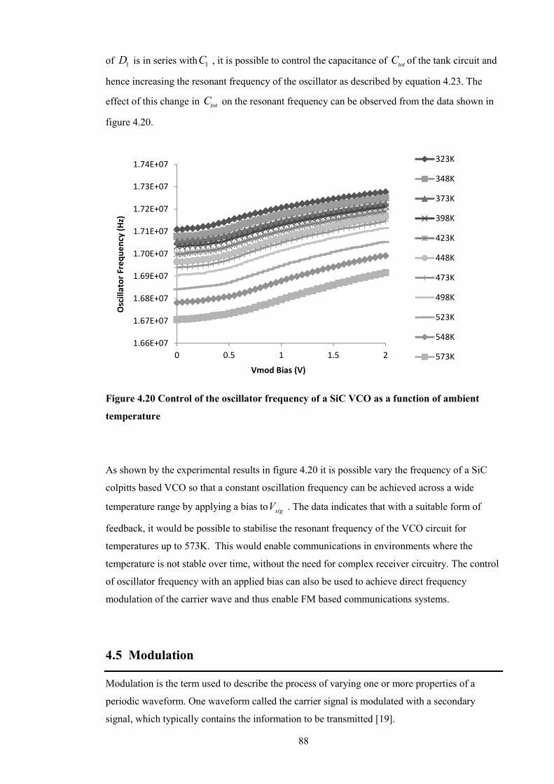
88
of 1D is in series with 1C , it is possible to control the capacitance of totC of the tank circuit and
hence increasing the resonant frequency of the oscillator as described by equation 4.23. The
effect of this change in totC on the resonant frequency can be observed from the data shown in
figure 4.20.
Figure 4.20 Control of the oscillator frequency of a SiC VCO as a function of ambient
temperature
As shown by the experimental results in figure 4.20 it is possible vary the frequency of a SiC
colpitts based VCO so that a constant oscillation frequency can be achieved across a wide
temperature range by applying a bias tosigV . The data indicates that with a suitable form of
feedback, it would be possible to stabilise the resonant frequency of the VCO circuit for
temperatures up to 573K. This would enable communications in environments where the
temperature is not stable over time, without the need for complex receiver circuitry. The control
of oscillator frequency with an applied bias can also be used to achieve direct frequency
modulation of the carrier wave and thus enable FM based communications systems.
4.5 Modulation
Modulation is the term used to describe the process of varying one or more properties of a
periodic waveform. One waveform called the carrier signal is modulated with a secondary
signal, which typically contains the information to be transmitted [19].
1.66E+07
1.67E+07
1.68E+07
1.69E+07
1.70E+07
1.71E+07
1.72E+07
1.73E+07
1.74E+07
0 0.5 1 1.5 2
Osc
illa
tor
Fre
qu
en
cy (
Hz)
Vmod Bias (V)
323K
348K
373K
398K
423K
448K
473K
498K
523K
548K
573K
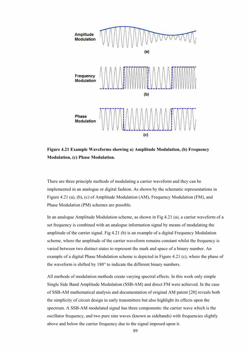
89
Figure 4.21 Example Waveforms showing a) Amplitude Modulation, (b) Frequency
Modulation, (c) Phase Modulation.
There are three principle methods of modulating a carrier waveform and they can be
implemented in an analogue or digital fashion. As shown by the schematic representations in
Figure 4.21 (a), (b), (c) of Amplitude Modulation (AM), Frequency Modulation (FM), and
Phase Modulation (PM) schemes are possible.
In an analogue Amplitude Modulation scheme, as shown in Fig 4.21 (a), a carrier waveform of a
set frequency is combined with an analogue information signal by means of modulating the
amplitude of the carrier signal. Fig 4.21 (b) is an example of a digital Frequency Modulation
scheme, where the amplitude of the carrier waveform remains constant whilst the frequency is
varied between two distinct states to represent the mark and space of a binary number. An
example of a digital Phase Modulation scheme is depicted in Figure 4.21 (c), where the phase of
the waveform is shifted by 180° to indicate the different binary numbers.
All methods of modulation methods create varying spectral effects. In this work only simple
Single Side Band Amplitude Modulation (SSB-AM) and direct FM were achieved. In the case
of SSB-AM mathematical analysis and documentation of original AM patent [20] reveals both
the simplicity of circuit design in early transmitters but also highlight its effects upon the
spectrum. A SSB-AM modulated signal has three components: the carrier wave which is the
oscillator frequency, and two pure sine waves (known as sidebands) with frequencies slightly
above and below the carrier frequency due to the signal imposed upon it.

90
In the case of FM modulation the spectrum deviates away from a centre frequency provided by
the oscillator, creating a band of frequencies which contain transmitted power dependant upon
the frequency of the modulated data source. The true frequency spectrum of a FM signal has
components extending infinitely, although their amplitude decreases and higher-order
components are often neglected in practical design problems. [21, 22]
4.5.1 High temperature Amplitude Modulation
Figure 4.22 Schematic block diagram of an analogue AM communications system
Figure 4.22 shows a schematic representation of an analogue Amplitude Modulation (AM)
communications system. Here the analogue signal relates to the measurand of the sensor and
could be produced using a sensor either directly or through amplification electronics. AM
modulation can be achieved by varying the amplitude of the oscillator output depending on the
magnitude of the sensor signal utilising a mixer circuit. This creates a simple communications
system, where the signal can then be amplified into the antenna for transmission.
Utilising SPICE models for the silicon carbide components in the circuit (i.e. the JFET and
Schottky diode) in combination with the temperature dependence of the passive component
characteristics, it is possible to design, simulate and construct a high temperature colpitts
oscillator. In this work the world’s first demonstration of amplitude modulation at 280°C was
realised [23].
Referring back to the schematic representation of the Colpitts oscillator shown in Figure 4.15,
the capacitance of 1C and 2C were 68pF and 82pF respectively and were selected from the large
number of devices fabricated on a single die for their low leakage current under applied bias, as

91
discussed in the previous chapter. A high temperature printed circuit board fabricated using a
commercial ceramic substrate with electrochemically deposited gold tracks was fabricated. The
electrical tracks included a spiral inductor designed for an inductance of 1.4µH, designed to
give an oscillation frequency of approximately 22MHz using equation 3.39. The output of the
oscillator was connected to a 1KΩ load resistor and the circuit was powered from a 12V DC
supply, connected to the drain of the JFET (denoted by Q in figure 4.18).
Figure 4.23 Spice simulation of the self starting of a Colpitts oscillator
Simulation of the circuit performance using a SPICE tool (Multisim 9.0 by National
Instruments) and the JFET models developed in the previous chapter show that the oscillator is
capable of self starting, as can be seen from the data shown in figure 4.23. A further
modification to the Colpitts oscillator by the addition of a second transistor in the output stage
of the circuit, as shown schematically in figure 4.24, enables amplitude modulation of the
oscillation.
It is possible the change the amplitude of the feedback signal observed at the gate of JFET 1Q ,
by utilizing the second JFET, denoted as 2Q , as a variable resistor. Using a negative bias on the
gate of 2Q , which behaves in a manner similar to the input bias sigV in figure 4.18, it is possible
to control the channel resistance of the JFET channel and therefore the magnitude of the
feedback signal to the gate of 1Q . This allows direct control of the amount of power that the
oscillator passes through the JFET thus controlling the amplitude of the wireless signal.
-6.00E+00
-4.00E+00
-2.00E+00
0.00E+00
2.00E+00
4.00E+00
6.00E+00
8.00E+00
1.00E+01
0.0
E+
00
2.0
E-0
7
4.0
E-0
7
6.0
E-0
7
8.0
E-0
7
1.0
E-0
6
1.2
E-0
6
1.4
E-0
6
Vo
lta
ge
(V
)
Time (S)
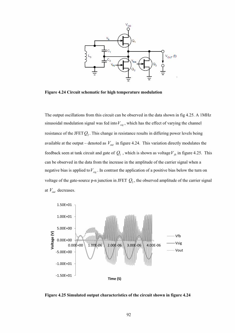
92
Figure 4.24 Circuit schematic for high temperature modulation
The output oscillations from this circuit can be observed in the data shown in fig 4.25. A 1MHz
sinusoidal modulation signal was fed intosigV , which has the effect of varying the channel
resistance of the JFET 2Q . This change in resistance results in differing power levels being
available at the output – denoted as outV in figure 4.24. This variation directly modulates the
feedback seen at tank circuit and gate of 1Q , which is shown as voltagefbV in figure 4.25. This
can be observed in the data from the increase in the amplitude of the carrier signal when a
negative bias is applied tosigV . In contrast the application of a positive bias below the turn on
voltage of the gate-source p-n junction in JFET 2Q , the observed amplitude of the carrier signal
at outV decreases.
Figure 4.25 Simulated output characteristics of the circuit shown in figure 4.24
-1.50E+01
-1.00E+01
-5.00E+00
0.00E+00
5.00E+00
1.00E+01
1.50E+01
0.00E+00 1.00E-06 2.00E-06 3.00E-06 4.00E-06
Vo
lta
ge
(V
)
Time (S)
Vfb
Vsig
Vout

93
This can ultimately be used to create an amplitude modulated signal at the JFET gate which is
also the signal transmitted through the inductor. In order to experimentally verify these
simulations, a hybrid module was then assembled using a 1mm thick aluminium nitride
substrate, onto which a seed layer of 10nm chrome was deposited followed by 250nm of ebeam
deposited gold. The gold layer on the substrate was then electroplated to a thickness of
approximately 8 µm, to reduce track resistance of both the interconnects and spiral inductor.
The capacitors used in this circuit were HfO2 dielectric MIM capacitors with a thickness of
60µm and had electrical values of 68pF and 82pF for C1 and C2 respectively. The devices were
selected after characterisation based on the low leakage current demonstrated, with both devices
showing a leakage current in the low µA range at a bias of 5V. The spiral inductor, 3L , was a
gold spiral patterned directly onto the substrate, which was measured using an Agilent 4284A
LCR bridge at 1MHz, showing an inductance of 1.4µH and a resistance of 4.8Ω. These values
match those predicted theoretically, using the equations and method described in section 3.6.
The high temperature hybrid circuit was realised by bonding the capacitors and JFETs to pads
on the gold interconnects using SilverPrint epoxy and baked in ambient conditions at 150°C for
1 hour before the electrical connections were made using wedge bonding with 20µm gold wire.
The circuit was heated using a pyrolytic boron nitride ceramic heater controlled by a Lakeshore
model 325 temperature controller. The power to the circuit was supplied from an Agilent
E3640A DC Power Supply, with the modulation signal to the gate of 3Q controlled with a
Keithly 2410 Source Meter, using probes directly on to the gold interconnects. The frequency
spectrum of the oscillator was measured using an Anritsu MS2721B Spectrum Master analyser
connected directly to outV and the amplitude of the RF signal was measured through an external
aerial attached to a Tektronix TDS3045C oscilloscope.
With the gate to 3Q held at -8V, the application of a modulation signal to the gate of the control
JFET 2Q varied the amplitude of the output signal as shown by the data in Fig. 4.25. For biases
between -2.5V and approximately -3.5V, a more negative modulation voltage increases the
channel resistance for JFET Q2. As previously described this results in a higher power level at
the point denoted by Vout and so an increased magnitude of the output signal is observed.

94
Figure 4.26 Relative amplitude of the output signal with varying voltage bias
After this point the resistance of the JFET ( 2Q ) channel begins to reduce the amount of current
flowing through the circuit, thus causing the amplitude of the signal to decrease. The results
show that it is possible to vary the voltage to achieve amplitude modulation in two bias regions
which are indicated as A and B in figure 4.26.
Figure 4.27 Signal amplitude as a function of voltage bias in region A
0
0.2
0.4
0.6
0.8
1
1.2
-6 -5.5 -5 -4.5 -4 -3.5 -3 -2.5
Re
lati
ve
Sig
na
l A
mp
litu
de
Signal Voltage (V)
Relative Signal Amplitude
y = -0.7275x2 - 4.6821x - 6.6305
R² = 0.9993
0
0.1
0.2
0.3
0.4
0.5
0.6
0.7
0.8
0.9
1
-3 -2.9 -2.8 -2.7 -2.6 -2.5
Sig
na
l A
mp
litu
de
(N
orm
ali
sed
)
Voltage Bias (V)
Relative Signal
Amplitude
Poly. (Relative Signal
Amplitude)
Region B Region A

95
However using the higher bias region (denoted as B) the oscillations showed an increase in
frequency with increasing bias. This is a non-desirable result from a circuit perspective as it
would require a high level of sophistication in the receiver electronics and therefore region A
was utilised in the modulation of the oscillators amplitude. As shown by the data in figure 4.27,
the observed output modulation in this region is not linear due to the transconductance of the
JFET. The applied gate voltage does not increase the channel resistance linearly, but instead
follows a square law relationship as is expected from theoretical consideration of the JFET
operation, as discussed in section 3.2.
The frequency spectrum of the oscillator operating at 280°C is shown by the data in fig. 4.28.
Here the gate of 2Q was held at a bias of -3.5 Volts to coincide with the maximum signal
amplitude, as shown by the data in figure 4.26. The observed peak frequency of the module
was 65dBm above the background noise, with a full half width maximum of approximately 7.2
kHz.
Due to the lack of an RF output amplifier coupled to the Colpitts oscillator the circuit would
have been unable to drive the 50 Ohm impedance of the input to an Anritsu spectrum analyser
antenna port. The construction of the test rig to heat the circuit to 280°C and the expense of RF
probe was prohibitive. The Anritsu spectrum analyser was placed within 1m of the oscillator
which a low frequency antenna attached.
Figure 4.28 Frequency spectrum of AM colpitts oscillator at 280°C
The frequency of the oscillations was measured as a function of temperature to determine the
shift. As shown by the data in Figure 4.29, the frequency drops with increasing temperature and
this decrease is dominated by the increase in capacitance density observed in the HfO2 MIM
-120
-110
-100
-90
-80
-70
-60
-50
-40
19.2 19.3 19.4 19.5 19.6
Sig
na
l a
mp
litu
de
(d
Bm
)
Frequency (MHz)

96
capacitors [24, 25], but also the parasitic capacitances within the SiC JFET increase with
temperature. These effects can be seen in figure 4.29 where the peak frequency can be seen to
shift down in value as a direct result of capacitance density increase.
Figure 4.29 Oscillation frequency of a colpitts oscillator as a function of temperature
The data shown in figure 4.30 shows a decrease in signal amplitude with an increase in
temperature whilst 2Q is held at -3.5V to obtain maximum amplitude and transmitted power.
The data shown in figure 4.30 demonstrates that the amplitude of the oscillator signal decreases
with temperature. For a high temperature communications system based on Amplitude
Modulation to be effective, a method for stabilising the signals amplitude with temperature
increased would need to be constructed. This outlines the disadvantage of AM as a modulation
scheme, as it becomes more difficult to separate an intentional amplitude modulated sensor
signal from the background effects on the components caused by elevated temperature.
-120
-110
-100
-90
-80
-70
-60
-50
-40
19.35 19.4 19.45 19.5 19.55
Sig
na
l A
mp
litu
de
(d
Bm
)
Frequency (MHz)
Increasing Temperature

97
Figure 4.30 Maximum signal amplitude as a function of temperature
4.5.2 High Temperature Frequency Modulation
It is highly likely that hostile environments will include sources of radio frequency interference
or noise which will significantly reduce the fidelity of any data transmitted using an amplitude
modulation based system. Frequency Modulation communication schemes are inherently more
resilient to these sources of noise than Amplitude Modulation schemes [19] and so they are
more likely to be suitable for deployment in these environments. Furthermore FM requires a
wider signal bandwidth than amplitude modulation by an equivalent modulating signal; this also
makes the signal more robust against noise and interference. Frequency modulation is also more
robust against signal-amplitude-fading phenomena.
Shown in figure 4.31 is a schematic block diagram of a conceptual Frequency Modulated
communication system.
Figure 4.31 Block diagram of simple FM Transmitter
As demonstrated by the data from the high temperature voltage controlled oscillator discussed
in section 4.3.1, it is possible to create high temperature circuits capable of direct frequency
-60
-58
-56
-54
-52
-50
-48
-46
303 353 403 453 503 553
Sig
na
l A
mp
litu
de
(d
Bm
)
Temperature (K)

98
modulation. By replacing the Oscillator and Mixer sections of the circuit depicted schematically
in Figure 4.22 with a high temperature colpitts VCO, direct frequency modulation of the carrier
waveform can be achieved [26].
One possible utilisation of this concept is in a sensing application, where the sensor signal
would pass through filtering and amplification (signal conditioning) circuits, before being
applied directly to the Varactor diode controlling the frequency of a voltage controlled
oscillator. This Frequency Modulated signal would then be amplified and fed into an antenna to
create an analogue Frequency Modulated signal which is controlled by the sensor and hence act
as a simple communications system.
However the communications scheme could also be digital, as shown in figure 4.21 (b). This
form of digital communication scheme is called Frequency Shift Keying (FSK), in contrast to
the Amplitude modulated counterpart, which is called Amplitude Shift Keying (ASK). In a
realistic circuit which is not based on the use of high performance digital circuitry, Frequency
Shift Keying is achieved by the choice of two frequencies (or more in the case of Multiple
Frequency Shift Keying (MFSK)) to represent digital information. Similarly Amplitude Shift
Keying can be achieved by choosing and transmitting two or more amplitudes (MASK) of the
same frequency to represent digital information.
Utilising the circuit shown in figure 4.18, a demonstration into the feasibility of Frequency Shift
Keying at high temperature was conducted. A separate hybrid circuit was measured at
temperatures up to 300°C through the use of a hotplate in the same fashion as discussed in the
previous section. The oscillation frequency of the circuit for different levels of reverse bias
applied to the Schottky diode ( 1D ) was measured and the resulting data are shown in figure
4.32. The data shows that there are regions where the frequency of the oscillator can be
controlled linearly by the application of an external voltage to 1D in the range of 0.75 and 1.5V
across the entire temperature range studied.

99
Figure 4.32 Linear regions of oscillator frequency change
The data in figure 4.33 shows binary Frequency Shift Keyed modulation from the silicon
carbide oscillator circuit operating at 300°C. The measurements were captured by an Anritsu
spectrum analyser connected to the circuit output. The data shows two distinct peaks,
corresponding to the frequencies produced by the oscillator when digital signals are applied
directly to a Voltage controlled oscillator circuit which is identical to controlling the capacitance
on a Schottky diode as discussed in section 3.2.4.
16700000
16800000
16900000
17000000
17100000
17200000
17300000
0.75 0.95 1.15 1.35
Fre
qu
en
cy (
Hz)
Voltage (V)
323K
348K
373K
398K
423K
448K
473K
498K
523K
548K
573K

100
Figure 4.33 Spectrum showing Frequency shift keyed Modulation (where 0 is the
frequency of the carrier waveform)
Among the different modulation schemes available, Frequency shift keying systems are the
most power efficient. This is highly beneficial for sensing systems which are often designed to
be self powered from energy harvested from the ambient environment. The most significant
disadvantage is the highly inefficient use of bandwidth whereby all frequencies between the
carrier frequency and the shift key frequency cannot be utilised [27]. However there is a special
case of Frequency Shift Keyed Modulation, Minimum Shift Keying, which can be viewed as an
attractive alternative to the more commonly used Phase Shift Keyed Modulation.
4.6 Conclusions
This chapter demonstrated the importance of accurate modelling of components to determine
high temperature oscillator frequencies. Numerical, simulation and experimental results of a
high temperature oscillator have demonstrated that all parasitic elements must be considered in
calculating an accurate oscillation frequency.
-90
-85
-80
-75
-70
-65
-60
-55
-50
-45
-40 -20 0 20 40 60
Am
pli
tud
e (
dB
)
Frequency (KHz)

101
This work demonstrated the world’s first high temperature wireless transmitters, with both
Amplitude Modulation (AM) and Frequency Modulation (FM) communication circuits capable
of operation at 573K achieved for the first time.
The AM oscillator operated at a maximum temperature of 553K and at a frequency of 19.4MHz
with a signal amplitude 65dBm above background noise. Realised from JFETs and HfO2
capacitors, modulation of the output signal was achieved by varying the load resistance by use
of a second SiC JFET. By applying a negative signal voltage of between -2.5 and -3V, a 50%
reduction in the signal amplitude was achieved. Temperature drift in the characteristics was also
observed, with a decrease in resonant frequency of almost 200 kHz when the temperature
changed from 300K to 573K. This decrease is due to the increase in capacitance density of the
HfO2 MIM capacitors and increasing junction capacitances of the JFET used as the amplifier
within the oscillator circuit. [21]
Direct frequency modulation of a SiC voltage controlled oscillator was demonstrated at a
temperature of 573K with a resonant frequency of 17MHz. The circuit was realised from an SiC
JFET and AlN capacitors with a SiC Schottky diode (SBD) used as a varactor. It was possible to
vary the frequency of oscillations by 100kHz with an input signal no greater than 1.5V being
applied to the SiC SBD. The effects of temperature drift were more dramatic in comparison to
the AM circuit at 400 KHz over the entire temperature range, a result of the properties of the
AlN film which causes the capacitors to increase in capacitance density by 10%. [26]
The physical design of the Colpitts oscillator specifically lends itself to miniaturisation,
featuring a capacitive feed-back path, over the inductive feed-back path in the Hartley oscillator.
This not only provides greater frequency stability, but the design naturally lends itself to
miniaturisation by incorporating on chip capacitors due to the compact design and use of
physically smaller components, whether they are discrete or incorporated on chip.
The Colpitts oscillator also demonstrates an inherently more powerful self starting ability than
the Clapp oscillator, which results in the allowed utilisation of lower value components, which
are typical of those used in the development of prototypes. [13] This work demonstrates that LC
oscillators provide a simple solution for producing high frequency sine waves. These circuits
contain a tuned LC tank and an active device arranged in an amplifier layout, they are
particularity useful in situations where the energy supply can be intermittent due to their self
starting ability [28].

102
4.7 References
[1] A. A. Andronov, Theory of Oscillators
[2] Jensen, J., "An Improved Square-Wave Oscillator Circuit," Circuit Theory, IRE
Transactions on , vol.4, no.3, pp.276,279, Sep 1957
[3] Irving Gottlieb, Practical Oscillator Handbook
[4] L. S. Senhouse, An Epitaxial planar structure for the Unijunction Transistor, IEEE
Tansactions on Electron Devices, Vol ED-16, No. 2, Feb 1969
[5] K. Vassilevski, Silicon Carbide Diodes for microwave applications, IJHSES, Vol. 15, No. 4
899-930 (2005)
[6] K. V. Vassilevski, Experimental observation of microwave oscillations produced by pulsed
silicon carbide IMPATT diode, Electronic Letter,s 29th March 2001 Vol. 37 No. 7
[7] Razavi B., Design of Analog CMOS Integrated Circuits. – Boston: McGraw–Hill, 2001.
[8] Robert J. Trew, The Potential of Diamond and SIC Electronic Devices for Microwave and
Millimeter-Wave Power Applications, Proceeding of the IEEE, Vol. 79, No. 5 , May 1991
[9] Warner, A.W., "Ultra-Precise Quartz Crystal Frequency Standards," Instrumentation, IRE
Transactions on , vol.I-7, no.3, pp.185,188, Dec. 1958
[10] Yoder, Hatten S., High-low quartz inversion up to 10,000 bars, Transactions, American
Geophysical Union, Volume 31, Issue 6, p. 827-835
[11] Sanitram Kal, Basic Electronics: Devices, Circuits and IT Fundamentals
[12] Oscar De Feo et al, The Colpitts Oscillator: Families of periodic solutions and their
Bifurcations, Int. J. Bifurcation Chaos 10, 935 (2000).
[13] V. V. Ulansky, Mathematical modelling of voltage-controlled oscillators with the Colpitts
and Clapp topology, ISSN 1990-5548 2009.
[14] Leenarts D., Van der Tang J., Vaucher C. Circuit design for RF transceivers. – Boston:
Kluwer. Academic Publishers, – 2001. – 311 p.
[15] O`Connor C. Develop a trimless voltage-controlled oscillators // Microwaves and RF. –
January 2000. – P. 94 – 105.
[16] Christer M. Andersson, A SiC Varactor With Large Effective Tuning Range for
Microwave Power Applications, IEEE Electron Device Letters, Vol. 32, No. 6, June 2011

103
[17] Wright, N.G.; Knights, A.P.; O'Neill, A.G.; Johnson, C.M., "Evaluation of 4H-SiC varactor
diodes for microwave applications," High Performance Electron Devices for Microwave and
Optoelectronic Applications, 1999. EDMO. 1999 Symposium on , vol., no., pp.301,306, 1999
[18] Arrl Handbook 2015
[19] Jyrki T. J. Penttinen The Telecommunications Handbook: Engineering Guidelines for
fixed, mobile and Satellite systems.
[23] D. Brennan, Amplitude Shift Keyed Radio Communications for Hostile Environments,
Material Science Forum, Vol 645-648, May 2010
[24] B. Miao et al, J. Appl. Phys., Vol. 104 (2008), p. 054510
[25] Bing Miao et al, Radiation Induced Change in Defect Density in HfO2 Based MIM
Capacitors, IEEE Transactions on Nuclear Science, 2009
[26] D. Brennan, Direct Frequency Modulation of a High Temperature Silicon Carbide
Oscillator, Material Science Forum, Vol 717-720, May 2012
[27] R. de Buda, Coherent Demodulation of Frequency-Shift Keying with Low Deviation Ratio,
IEEE Transactions on Communications, Vol. 7 No. 3, June 1972
[28] Nhat M. Nguyen, Start-up and Frequency Stability in High-Frequency Oscillators, IEEE
Journal of solid state circuits, Vol. 27, No. 5, May 1992
104
Chapter 5: Energy Harvesting in Extreme
Environments
5.1 Introduction
In chapter 3 the characteristics of both active and passive high temperature components were
discussed and their suitability for use in creating elevated temperature circuits considered.
Chapter 4 described the construction of oscillator circuits operable at high temperature and how
these form the basis for numerous electronic systems, including communication systems.
Circuits containing devices fabricated from silicon carbide have the ability to operate in extreme
environments, including those with high temperature and high radiation flux. These
environments are dangerous and in the case of high radiation dose, potentially lethal to humans
and therefore maintenance of any electronic system placed within such an environment is
required to be minimal [1, 2]. This places significant constraints on the system in regard to the
power available during operation: either the power consumption must be in the nW range or the
circuit must become self sufficient by harvesting its energy requirements from the ambient. For
a wireless sensor node, the power required for the communication of data requires a power level
that is closer to the mW level, especially in an electrically noisy environment and so this
precludes the design of a circuit with nW consumption. Hence, the desire to place wireless
sensor nodes in extreme environments will require the realisation of energy harvesting and
power control circuits that can operate in these hostile conditions. This requirement is not a
factor when developing traditional silicon wireless sensor modules, which allow a system
designer more flexibility when choosing a power source. Usually a silicon based wireless sensor
node is designed with a battery for the power source, as it offers simple replacement, but the
hostility of the environment in which silicon carbide components can operate severely restricts
the choice of battery. For example the majority of commercial batteries are not rated for
temperatures above 85°C and zebra batteries contain chemicals such as lithium that are not
suitable for use in high radiation dose environments.
These factors combined with the explosion of research literature in the field of energy
harvesting devices for powering traditional silicon based wireless sensor nodes, supports the
vision of silicon carbide based wireless sensor nodes that are powered from energy harvested
from the extreme conditions in the environment. This chapter describes the development of the
world’s first energy harvesting system in silicon carbide technology designed to power a radio
frequency communications system similar to those described in chapter 4.

105
5.2 Experimental
5.2.1 Energy harvesting technologies
There are multiple sources of ambient energy which are accessible in a typical hostile
environment, including vibration, thermal gradients and light. In this study, the intended
application is a monitoring system on the primary coolant loop of a nuclear reactor, so that the
temperature on the loop is approximately 300°C [3] with an ambient of around 50°C in an
environment lit by fluorescent tubes. Each of these energy sources requires a different
technique to convert the energy into a useable DC power supply, whilst in conventional silicon
electronics power levels and efficiency are optimised, experimental techniques discussed in the
previous chapter demonstrate SiC RF circuits need to be in the region of 10mA at 12V.
5.2.2 Vibrational Energy Harvesting
Harvesting energy from vibrational sources requires either an electromagnetic energy harvester
[4] or alternatively a piezoelectric material [5]. The physical method for generating energy from
these sources is similar and features a structure such as a cantilever or spring with the ability to
move.
Figure 5.1 Examples of (a) an electromagnetic energy harvester and (b) a Piezoelectric
energy harvester [5]
Figures 5.1(a) and (b) show schematic diagrams of an electromagnetic harvester and a
piezoelectric harvester. In general techniques to harvest vibrations are less well developed than
both light and heat energy harvesting technologies. For example more research is required into
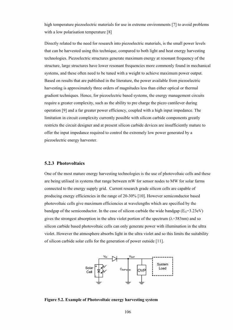
106
high temperature piezoelectric materials for use in extreme environments [7] to avoid problems
with a low polarisation temperature [8]
Directly related to the need for research into piezoelectric materials, is the small power levels
that can be harvested using this technique, compared to both light and heat energy harvesting
technologies. Piezoelectric structures generate maximum energy at resonant frequency of the
structure, large structures have lower resonant frequencies more commonly found in mechanical
systems, and these often need to be tuned with a weight to achieve maximum power output.
Based on results that are published in the literature, the power available from piezoelectric
harvesting is approximately three orders of magnitudes less than either optical or thermal
gradient techniques. Hence, for piezoelectric based systems, the energy management circuits
require a greater complexity, such as the ability to pre charge the piezo cantilever during
operation [9] and a far greater power efficiency, coupled with a high input impedance. The
limitation in circuit complexity currently possible with silicon carbide components greatly
restricts the circuit designer and at present silicon carbide devices are insufficiently mature to
offer the input impedance required to control the extremely low power generated by a
piezoelectric energy harvester.
5.2.3 Photovoltaics
One of the most mature energy harvesting technologies is the use of photovoltaic cells and these
are being utilised in systems that range between mW for sensor nodes to MW for solar farms
connected to the energy supply grid. Current research grade silicon cells are capable of
producing energy efficiencies in the range of 20-30% [10]. However semiconductor based
photovoltaic cells give maximum efficiencies at wavelengths which are specified by the
bandgap of the semiconductor. In the case of silicon carbide the wide bandgap (EG=3.23eV)
gives the strongest absorption in the ultra violet portion of the spectrum (λ=383nm) and so
silicon carbide based photovoltaic cells can only generate power with illumination in the ultra
violet. However the atmosphere absorbs light in the ultra violet and so this limits the suitability
of silicon carbide solar cells for the generation of power outside [11].
Figure 5.2. Example of Photovoltaic energy harvesting system

107
Shown in figure 5.2 is an example of a simple energy harvesting system utilising a photovoltaic
cell, here it is assumed that the solar cell can produce a voltage sufficiently high enough to
power the system load. Work in the literature has shown that it is possible to use SiC PiN diodes
to charge up hafnium dioxide capacitors using a Schottky diode to prevent reverse leakage back
into the cell. It should be noted however that both the current generated and the storage
capacitors in this work were too small to actually power a system load. It does however
demonstrate the possibility of utilising larger PiN diodes or an array to provide enough power
for a system load. [12]
5.2.4 Thermoelectric harvesters
Thermoelectric generators (TEGs) are energy harvesting devices capable of producing relatively
large current levels, at lower voltages which are typically in the order of one volt. They act as
heat engines by harvesting energy from the heat flow generated by a thermal gradient across the
device through a phenomenon known as the Seebeck effect [13]. The figure of merit for a
thermoelectric material for a given application is determined by ZT, where T is the absolute
temperature, and Z is the figure of merit defined as:
2Z Sk
σ= 5.1
Where S is the Seebeck coefficient, σ is the electrical conductivity, and k is the thermal
conductivity. [13]
Equation 5.1 indicates that a good Thermoelectric (TE) material must have a high Seebeck
coefficient, high electrical conductivity, and low thermal conductivity. Currently available TE
materials used in commercial devices for power generation are alloys of PbTe with ZT = 1 at
500°C and SiGe with ZT = 0.6 at 700C, values for ZT are varied across the literature and these
values are to give example of possible ZT. [14] Figure 5.2 shows typical variation of ZT as a
function of temperature for different commercially relevant TE materials

108
Figure 5.2. ZT values of numerous different TE materials [15]
Thermoelectric generators are constructed out of pairs of ‘legs’ manufactured from p and n
semiconductor materials. These are connected electrically in series, but thermally in parallel
between a hot contact (heat source) and a heat sink (cool side), as shown in the structural
schematic in figure 5.3
Figure 5.3 Schematic cross section of a thermoelectric generator

109
In this work the performance of a standard off-the-shelf TEG manufactured by Marlow (product
number TG 12-801L with a face area of 1600mm2) was characterized in terms of the electrical
output as a function of temperature difference between the hot and cold surfaces. A ceramic
hotplate controlled by a Lakeshore temperature controller was used to provide a controlled
temperature heat source whilst a thermocouple embedded into the base of a heat sink cooled by
means of forced air cooling provided the cooler side, creating a measurable temperature gradient
across the device. The measurement system was closed loop controlled by a LabView program
and the electrical output from the commercial TEG used in this study is shown by the data in
Fig. 5.3.
Figure 5.3. Electrical Output of commercial TEG
As shown by the data in Figure 5.3, thermogenerators are capable of producing a power level of
around half a watt for a temperature difference of 59°C. This temperature difference is the
equivalent of placing a hot coffee on the upper surface of the generator. The data in the figure
also shows that the maximum power is delivered from the thermogenerator at half the maximum
voltage for any given temperature gradient. This point is referred to as the maximum power
point. It is worth noting that the voltage levels for the maximum power point are significantly
lower than the voltages used to run the oscillator circuits shown in chapter 4 and further are
smaller in magnitude than the gate voltage required to completely turn off a SiC JFET, as shown
by the data in section 3.3.3
0
0.05
0.1
0.15
0.2
0.25
0.3
0.35
0.4
0.45
0.5
0 0.5 1 1.5 2 2.5
Iou
t (A
mp
s)
Vout (Volts)
Minor Gradient
9 Degree Gradient
16 Degree Gradient
25 Degree Gradient
33 Degree Gradient
41 Degree Gradient
50 Degree Gradient
59 Degree Gradient

110
In order to run SiC electronic circuits effectively a higher power supply voltage will be required
from the generator. Whilst it is possible to use multiple generators connected electrically in
series to increase outV , whilst maintaining the current level, it requires a significant amount of
space. An alternative approach is to design a boost or step up converter to increase the voltage
from a single generator. This method has the potential to significantly reduce the space
requirement as electronic components are smaller than additional generators, however the
current level available to the silicon carbide circuit is reduced.
5.3 Step Up Converter
Fundamental to the operation of any magnetic boost converter is the tendency of an inductor or
transformer to resist changes in current. A physical inductor is created by controlling the shape
of a conductor and through the choice of the material with which it makes contact. In general
they consist of coils of wire wrapped around an insulating material to increase the inductance.
When current flows through an inductor, energy is stored temporarily in a magnetic field in the
coil, as this current changes, the time-varying magnetic field induces a voltage in the inductor
winding according to Faraday’s law of electromagnetic induction in the opposite direction to the
change in current. The inductance is related to the magnetic flux generated within the inductor
for a specified current flow, as expressed by equation 5.2.
Li
ϕ= 5.2
The current flowing through a conductor will generate a magnetic field, thus all conductors
show some inductance. In order to increase inductance, the conductor is shaped into a coil, this
increases the number of times the magnetic flux lines link the circuit, therefore increasing the
field and hence the inductance. By increasing the number of coils it is possible to increase the
inductance further. Further enhancement is possible by wrapping the conductor on a
ferromagnetic or ferrimagnetic material, so that the magnetising field from the coil will induce
magnetisation in the material, increasing the magnetic flux and hence the inductance. Any
change in current through an inductor creates a changing flux, which induces a voltage across
the inductor.
From Faraday’s Law of Induction the induced voltage can be expressed as;
dv
dt
φ= 5.3
Substituting equation 5.2 into 5.3 gives;

111
( )d div Li L
dt dt= = 5.4
Hence inductance is also a measure of the amount of electromotive force (voltage) generated per
unit change in current.
Figure 5.4, depicts a standard schematic representation of a step-up or boost converter topology.
The circuit topology is based on the use of a magnetic component, in the form of an inductor
that acts as an energy store, in conjunction with a switching device and a rectifying device.
Figure 5.4. Standard step-up converter topology
A step up converter has two distinct states; the switching element can either be open or closed
as is shown in figures 5.5 (a) and (b). With the switch closed current flows in a clockwise
direction in the circuit, through the inductor and switch. During this stage of the operation the
current flow through the inductor results in energy being stored in the magnetic field. The
potential at the left end of the inductor is positive as the right end is essentially connected to
ground, via the switch which is assumed to have a low on-state resistance.

112
Figure 5.5 Diagram showing current flow in the different operating states of a step up
converter
Once the switch has been opened, the current through the inductor is reduced as the impedance
of the circuit is increased, due to the low resistance connection to ground being removed. The
inductor opposes this change in current flow by inducing a voltage, which results in the polarity
of the inductor becoming reversed, i.e. the left side of the inductor becomes negative with
respect to the right. As a result the voltage across the inductor and the voltage source are
connected in series, resulting in a higher voltage, which charges the capacitor through the diode.
A boost converter has two modes of operation; continuous and discontinuous, the distinction
between these is controlled by the frequency of operation and the duty cycle which the switch is
open or closed. [16, 17, 18]
5.3.1 Continuous mode operation
When a boost converter is operated in continuous mode, the current flowing through the
inductor never falls to zero. Typical waveforms depicting the currents and voltages of a
converter operating in continuous mode are shown in figure 5.6. It can be seen that during onT
with the switch closed, the current through both the switch ( SI ) and inductor ( LI ) rises, then
when the switch is turned off the current flows through the diode ( DI ). In the case of an ideal
converter, without the inclusion of parasitic elements, the output voltage can be calculated using
the following analytical expressions.

113
Figure 5.6: Waveforms of current and voltage in a boost converter operating in
continuous mode
Whilst in the On-state, the switching component is closed, which makes the input voltage ( iV )
appear across the inductor, this causes a change in the current flowing through the inductor
during a time period (t), this can be represented by equation 5.5:
iLVI
t L
∆=
∆ 5.5
At the end of the On-state, the increase in the inductor current can be expressed as:
0
1on
DT
L i i
DTI V dt V
L L∆ = =∫ 5.6
Where D is the duty cycle, which represents the fraction of the commutation period during
which the switch is On. Therefore D ranges between 0 where the switch is never on and 1
where the switch is always on.
During the Off-state, the switch is open, so current flowing through the inductor flows through
the load. With ideal components, assuming a zero voltage drop across the onLI∆ diode, and a
capacitor large enough for its voltage to remain constant, thus:

114
L
i o
dIV V L
dt− − 5.7
Therefore, the variation of LI during the Off-period is:
( ) ( )( )1off
Ti o i o
LDT
V V dt V V D TI
L L
− − −∆ =∫ 5.8
Assuming the converter is operating in the steady-state condition, the amount of energy stored
in each of its components has to be the same at the beginning and at the end of a commutation
cycle. Specifically, the energy stored in the inductor is given by:
21
2 LE LI= 5.9
As the inductor current has to be the same at the start and end of the commutation cycle, the
overall change in current is zero:
0on offL LI I∆ + ∆ = 5.10
Substituting onLI∆ and
offLI by their expressions yields:
( ) ( )10
on off
i oi
L L
V V D TV DTI I
L L
− −∆ + ∆ = + = 5.11
This can be rewritten as:
1
1o
i
V
V D=
− 5.12
Thus we can also write
1 i
o
VD
V= − 5.13
This expression demonstrates that the output voltage is always greater than the input voltage (as
duty cycle goes from 0 to 1), and that it increases with increasing duty cycle.
5.3.2 Discontinuous mode operation
In discontinuous mode, the inductor may be completely discharged before the end of a whole
commutation cycle and this generally occurs when the converter has a low output current, often

115
referred to as operating under light loads. In this case, the current flowing through the inductor
falls to zero during part of the period as shown by the waveforms in figure 5.7.
Figure 5.7: Waveforms of current and voltage in a boost converter operating in
discontinuous mode.
The difference between continuous and discontinuous mode has a strong effect on the output
voltage equation. As the inductor current at the beginning of the cycle is zero, its maximum
value is given by:
Max
i
L
V DTI
L= 5.14
During the off-period, LI falls to zero after 2 sD T×

116
( ) 20
Max
i o s
L
V V D TI
L
− ×+ = 5.15
By combining equations 5.12 and 5.13, it is possible to obtain
2 i
s
o i
V DD T
V V× =
− 5.16
The load current, oI , is equal to the average diode current ( DI ). This can be seen in figure 5.7
where the diode current is equal to the inductor current during the off-state. Therefore the output
current can be expressed as:
22MAXL
o D s
II I D T= = × 5.17
Replacing the values with their respective expressions yields:
( )
2 2
2 2i i i
o
o i o i
V DT V D V D TI
L V V L V V× =
− − 5.18
Thus the output voltage gain can be written:
2
12
o i
i o
V V D T
V LI+ 5.19
Whilst this expression is more complex than used to describe continuous operation, it shows
that the output voltage gain not only depends on the duty cycle, but also the inductor value,
input voltage, switching frequency and the output current [19, 20].
Whilst working in the continuous mode would be beneficial in terms of mathematical
simplicity. Discontinuous mode is preferable in some situations particularly if you're operating
at low power levels, where losses due to ripple current isn't a significant factor in efficiency.
5.4 A Novel high temperature boost converter
Whilst a boost converter will operate with any switch, converters utilising this step up topology
usually employ a semiconducting device to provide the switching component. Any type of
semiconducting device can be used here, depending on the circuit application and power
requirements, the control for the switching of the converter can be as complex as a user requires.
In typical consumer electronics the switching device is usually an enhancement mode device
such as a MOSFET, and the control circuitry has the advantage of being able to run off a power
source with such as battery. These conditions, along with the progress in conventional CMOS
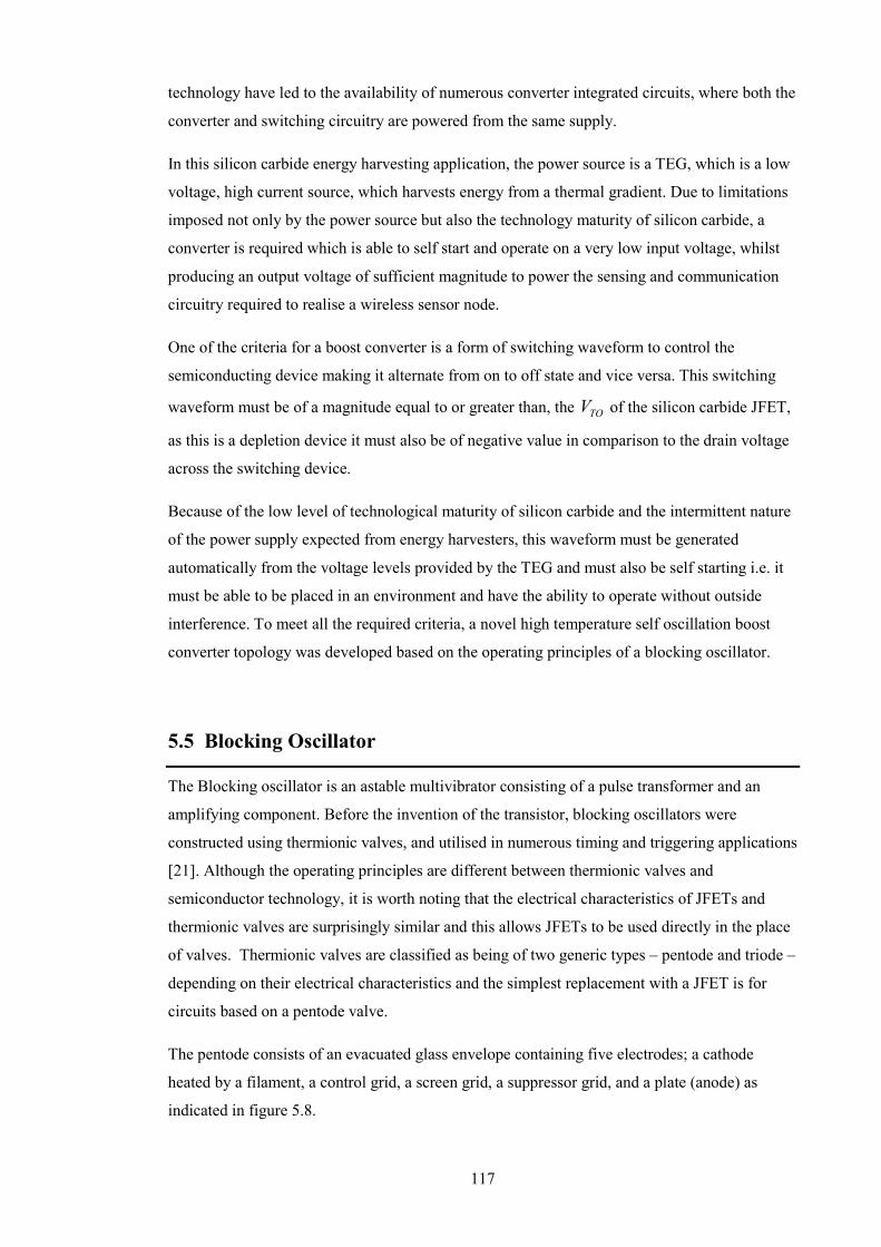
117
technology have led to the availability of numerous converter integrated circuits, where both the
converter and switching circuitry are powered from the same supply.
In this silicon carbide energy harvesting application, the power source is a TEG, which is a low
voltage, high current source, which harvests energy from a thermal gradient. Due to limitations
imposed not only by the power source but also the technology maturity of silicon carbide, a
converter is required which is able to self start and operate on a very low input voltage, whilst
producing an output voltage of sufficient magnitude to power the sensing and communication
circuitry required to realise a wireless sensor node.
One of the criteria for a boost converter is a form of switching waveform to control the
semiconducting device making it alternate from on to off state and vice versa. This switching
waveform must be of a magnitude equal to or greater than, the TOV of the silicon carbide JFET,
as this is a depletion device it must also be of negative value in comparison to the drain voltage
across the switching device.
Because of the low level of technological maturity of silicon carbide and the intermittent nature
of the power supply expected from energy harvesters, this waveform must be generated
automatically from the voltage levels provided by the TEG and must also be self starting i.e. it
must be able to be placed in an environment and have the ability to operate without outside
interference. To meet all the required criteria, a novel high temperature self oscillation boost
converter topology was developed based on the operating principles of a blocking oscillator.
5.5 Blocking Oscillator
The Blocking oscillator is an astable multivibrator consisting of a pulse transformer and an
amplifying component. Before the invention of the transistor, blocking oscillators were
constructed using thermionic valves, and utilised in numerous timing and triggering applications
[21]. Although the operating principles are different between thermionic valves and
semiconductor technology, it is worth noting that the electrical characteristics of JFETs and
thermionic valves are surprisingly similar and this allows JFETs to be used directly in the place
of valves. Thermionic valves are classified as being of two generic types – pentode and triode –
depending on their electrical characteristics and the simplest replacement with a JFET is for
circuits based on a pentode valve.
The pentode consists of an evacuated glass envelope containing five electrodes; a cathode
heated by a filament, a control grid, a screen grid, a suppressor grid, and a plate (anode) as
indicated in figure 5.8.

118
Figure 5.8. Circuit symbol of a pentode
With the addition of a screen and suppressor grid the pentode proved a far better voltage
amplifying device than the earlier triode and tetrode devices and had current-voltage
characteristics analogous to modern solid state transistors. The electrical characteristics shown
in figure 5.9 are the current-voltage behaviour of (a) a pentode device and (b) a silicon carbide
JFET device. It is worth noting that the pentode behaviour of the JFET structure is only true for
long channel devices operating in the low electric field regime and the existence of short
channel effects, as are commonly observed in high voltage power device structures [22] give
rise to triode type behaviour. Pentode valves became obsolete, overtaken by the progress made
by solid state transistors however they are still used today mainly in high power, high frequency
industrial applications, specifically radio transmission.
Figure 5.9. Comparison of representative I-V Characteristics of (a) Pentode thermionic
valve and (b) Silicon carbide JFET
The schematic in figure 5.10 shows a comparison of the simplest form of blocking oscillator
circuit based on the use of both valve and JFET technology which can be constructed as shown
in figure 5.10.
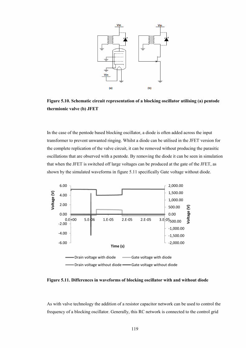
119
Figure 5.10. Schematic circuit representation of a blocking oscillator utilising (a) pentode
thermionic valve (b) JFET
In the case of the pentode based blocking oscillator, a diode is often added across the input
transformer to prevent unwanted ringing. Whilst a diode can be utilised in the JFET version for
the complete replication of the valve circuit, it can be removed without producing the parasitic
oscillations that are observed with a pentode. By removing the diode it can be seen in simulation
that when the JFET is switched off large voltages can be produced at the gate of the JFET, as
shown by the simulated waveforms in figure 5.11 specifically Gate voltage without diode.
Figure 5.11. Differences in waveforms of blocking oscillator with and without diode
As with valve technology the addition of a resistor capacitor network can be used to control the
frequency of a blocking oscillator. Generally, this RC network is connected to the control grid
-2,000.00
-1,500.00
-1,000.00
-500.00
0.00
500.00
1,000.00
1,500.00
2,000.00
-6.00
-4.00
-2.00
0.00
2.00
4.00
6.00
0.E+00 5.E-06 1.E-05 2.E-05 2.E-05 3.E-05
Vo
lta
ge
(V
)
Vo
lta
ge
(V
)
Time (s)
Drain voltage with diode Gate voltage with diode
Drain voltage without diode Gate voltage without diode

120
of the valve or in the case of the JFET circuit it is placed to provide negative feedback to the
gate connection as shown in figure 5.12.
Figure 5.12. JFET based blocking oscillator with RC control
The RC network can be used control the blocking oscillators frequency, but the variation in
frequency achieved by controlling either the capacitance or resistance are limited and
mathematical methods of deducing the accurate predictions of oscillator frequency are limited in
scope [23]. The properties of the transformer windings cause a greater variation in operating
frequency and as expected smaller valued inductances on both the primary and the secondary
cause the frequency of oscillation to increase.
5.5.1 Theory of JFET blocking oscillator without RC network
As mentioned in the previous section, an RC network can be used to vary the frequency of
oscillations in a blocking oscillator. However, its suitability for use in these circuits is limited
by the inability to accurately predict the fundamental oscillation frequency. It is apparent in the
simplest form of the blocking oscillator topology that no capacitor is required to produce
oscillations. In this case, the RC network is formed by the parasitic capacitances within the
FET and associated circuit. Following the conventional blocking oscillator theory for an RC
dominated oscillation frequency, the predicted value would be orders of magnitude higher than
observed experimentally. For example, using the junction capacitance of a similar JFET, which
was extracted in chapter 2 gives a value of approximately 27pF over the temperature range
studied. Utilising equation 4.5 with a primary inductance of 50µH primary inductance (which is
typical for the circuits described in this thesis) an oscillation frequency of approximately
4.5MHz is predicted, as shown in equation 5.20.

121
012 6
14.5
2 25 10 50 10f MHz
π − −= =
× × × 5.20
This leads to the general conclusion that frequency is determined by the relationship between
the transistor and the inductance of the transformer [16, 21]. Mathematical analysis of blocking
oscillators is not covered extensively in the literature and methods to predict frequency have
proved inaccurate. The majority of the literature concentrates on blocking oscillators
constructed using bipolar junction transistor structures and the formulas do not lend themselves
to describing a circuit based on the use of a JFET [23]. However the availability of SPICE now
allows circuit designers to simulate circuits more rapidly and through the use of SPICE and
numerical methods a novel formula to predict oscillation frequency is presented. This formula
is only based on the properties of the JFET transistor and the inductance of the transformer
windings.
SPICE simulations of the topology shown in figure 5.10 (which does not include the diode)
were performed. By varying the inductance of the primary and secondary windings, the
variation in the oscillation frequency was observed to change, as shown by the data in figure
5.13. By plotting 1
L for each of the primary inductances investigated, it becomes apparent
that frequency is determined by the reciprocal of the square root of the inductance.
Figure 5.13 Linear relationship between frequency and secondary inductance for different
primary inductance values, given in Henries.
0
20000
40000
60000
80000
100000
120000
0 20 40 60 80 100 120
Fre
qu
en
cy (
Hz)
1/√Secondary inductance
1.00E-04
2.00E-04
3.00E-04
4.00E-04
5.00E-04
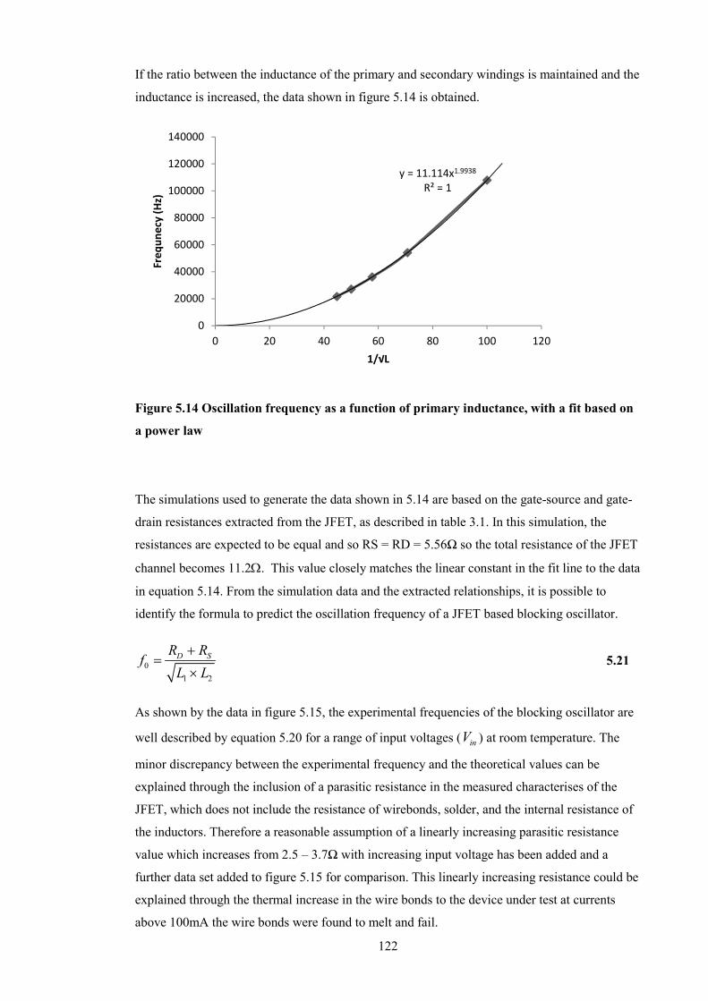
122
If the ratio between the inductance of the primary and secondary windings is maintained and the
inductance is increased, the data shown in figure 5.14 is obtained.
Figure 5.14 Oscillation frequency as a function of primary inductance, with a fit based on
a power law
The simulations used to generate the data shown in 5.14 are based on the gate-source and gate-
drain resistances extracted from the JFET, as described in table 3.1. In this simulation, the
resistances are expected to be equal and so RS = RD = 5.56Ω so the total resistance of the JFET
channel becomes 11.2Ω. This value closely matches the linear constant in the fit line to the data
in equation 5.14. From the simulation data and the extracted relationships, it is possible to
identify the formula to predict the oscillation frequency of a JFET based blocking oscillator.
0
1 2
D SR Rf
L L
+=
× 5.21
As shown by the data in figure 5.15, the experimental frequencies of the blocking oscillator are
well described by equation 5.20 for a range of input voltages ( inV ) at room temperature. The
minor discrepancy between the experimental frequency and the theoretical values can be
explained through the inclusion of a parasitic resistance in the measured characterises of the
JFET, which does not include the resistance of wirebonds, solder, and the internal resistance of
the inductors. Therefore a reasonable assumption of a linearly increasing parasitic resistance
value which increases from 2.5 – 3.7Ω with increasing input voltage has been added and a
further data set added to figure 5.15 for comparison. This linearly increasing resistance could be
explained through the thermal increase in the wire bonds to the device under test at currents
above 100mA the wire bonds were found to melt and fail.
y = 11.114x1.9938
R² = 1
0
20000
40000
60000
80000
100000
120000
140000
0 20 40 60 80 100 120
Fre
qu
ne
cy (
Hz)
1/√L
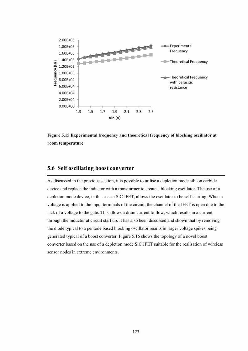
123
Figure 5.15 Experimental frequency and theoretical frequency of blocking oscillator at
room temperature
5.6 Self oscillating boost converter
As discussed in the previous section, it is possible to utilise a depletion mode silicon carbide
device and replace the inductor with a transformer to create a blocking oscillator. The use of a
depletion mode device, in this case a SiC JFET, allows the oscillator to be self-starting. When a
voltage is applied to the input terminals of the circuit, the channel of the JFET is open due to the
lack of a voltage to the gate. This allows a drain current to flow, which results in a current
through the inductor at circuit start up. It has also been discussed and shown that by removing
the diode typical to a pentode based blocking oscillator results in larger voltage spikes being
generated typical of a boost converter. Figure 5.16 shows the topology of a novel boost
converter based on the use of a depletion mode SiC JFET suitable for the realisation of wireless
sensor nodes in extreme environments.
0.00E+00
2.00E+04
4.00E+04
6.00E+04
8.00E+04
1.00E+05
1.20E+05
1.40E+05
1.60E+05
1.80E+05
2.00E+05
1.3 1.5 1.7 1.9 2.1 2.3 2.5
Fre
qu
en
cy (
Hz)
Vin (V)
Experimental
Frequency
Theoretical Frequency
Theoretical Frequency
with parasitic
resistance

124
Figure 5.16. Schematic of self oscillating boost converter topology
By replacing the inductor in the standard boost converter topology shown in figure 5.4 with a
transformer, it is possible to eliminate the need for a complex gate drive system by utilising the
properties of a blocking oscillator. Here the primary winding of the transformer acts as the
inductor, storing energy and providing the voltage enhancement required for operation of the
conventional converter topology. The secondary winding is counter wound in comparison to the
primary and this results in a negative voltage at the JFET gate, which acts to pinch off the
channel and turns off the FET.
The use of a transformer to generate a negative switching waveform relative to the supply
voltage is fundamental to the operation of the circuit at low input voltages. To create a
waveform which has a negative magnitude greater than the threshold voltage of the JFET
(which is typically in the order of -3V at room temperature), the number of turns on the
secondary winding must be greater than the primary. Standard transformer theory states that the
voltage induced on the secondary winding is greater than that across the primary in a ratio given
by the number of turns on the windings. This allows the boost converter to operate at voltages
lower in magnitude than Vto of the JFET, such as those generated by the thermoelectric
generator described in section 5.1.4.

125
Figure 5.17 Voltage and Current Waveforms of SOBC at room temperature
The data in figure 5.17, depicts the voltage waveforms seen at the JFET drain i.e. the voltage
across the primary winding, the gate voltage induced in the secondary winding of the
transformer, and the current flowing through the primary winding of the transformer (input
inductor) during room temperature operation.
The operation of the circuit can be described as follows;
At start up, the channel of the depletion mode silicon carbide JFET is conducting. Current
begins to flow through the primary winding of the transformer and the channel of the JFET to
ground. This is identical to the on state operation of a conventional boost converter, as described
in section 5.2. The change in current in the primary winding induces a negative bias in the
secondary winding, which is connected to the gate of the JFET. Current is drawn through the
diode of the JFET allowing for the negative voltage to increase. Further increases in the current
flowing through the primary winding causes the negative voltage on the secondary winding to
increase in magnitude and the channel of the JFET is progressively pushed towards pinch-off
this is indicated at point A in Figure 5.17.
Once the magnitude of the voltage on the secondary winding exceeds the threshold voltage of
the JFET, the JFET becomes non-conducting. This increase in channel resistance of the JFET
causes the magnetic field contained in the ferrite core of the transformer to collapse and the
voltage in the primary winding increases as is observed in a standard boost converter operation.
This point is denoted as B in figure 5.17. [24]
-0.5
0
0.5
1
1.5
2
2.5
3
3.5
4
-50
-40
-30
-20
-10
0
10
20
0 0.0005 0.001 0.0015 0.002 0.0025
Cu
rre
nt
in (
mA
*1
0)
Vo
lta
ge
(V
)
Time (s)Voltage in Primary Winding Voltage in Secondary Winding
Current in Primary Winding
A
B
C
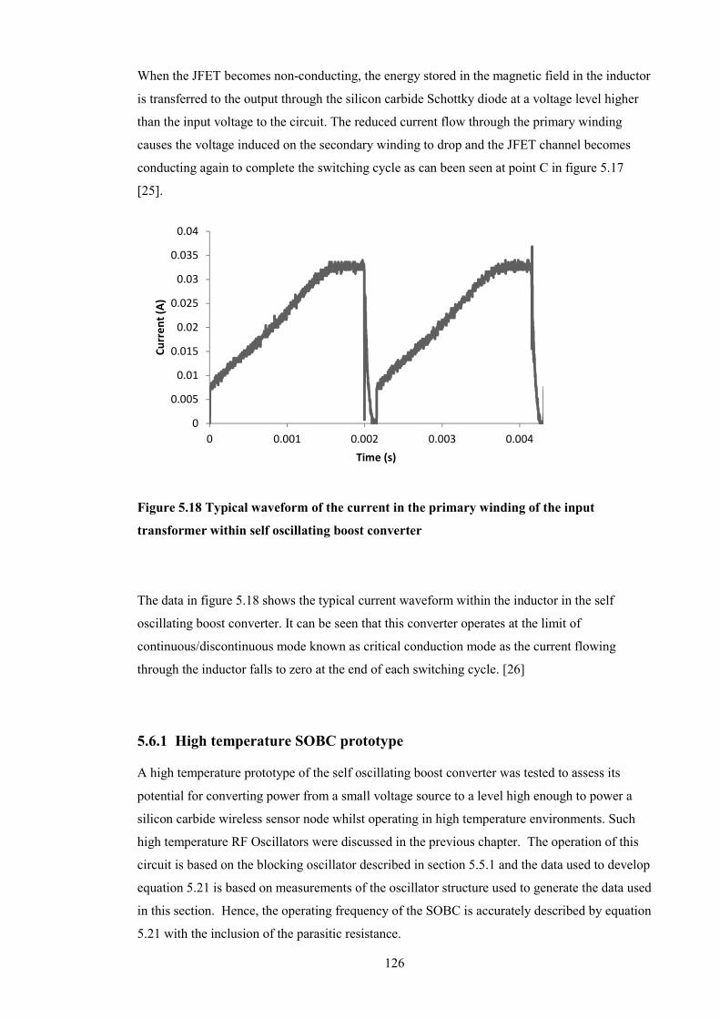
126
When the JFET becomes non-conducting, the energy stored in the magnetic field in the inductor
is transferred to the output through the silicon carbide Schottky diode at a voltage level higher
than the input voltage to the circuit. The reduced current flow through the primary winding
causes the voltage induced on the secondary winding to drop and the JFET channel becomes
conducting again to complete the switching cycle as can been seen at point C in figure 5.17
[25].
Figure 5.18 Typical waveform of the current in the primary winding of the input
transformer within self oscillating boost converter
The data in figure 5.18 shows the typical current waveform within the inductor in the self
oscillating boost converter. It can be seen that this converter operates at the limit of
continuous/discontinuous mode known as critical conduction mode as the current flowing
through the inductor falls to zero at the end of each switching cycle. [26]
5.6.1 High temperature SOBC prototype
A high temperature prototype of the self oscillating boost converter was tested to assess its
potential for converting power from a small voltage source to a level high enough to power a
silicon carbide wireless sensor node whilst operating in high temperature environments. Such
high temperature RF Oscillators were discussed in the previous chapter. The operation of this
circuit is based on the blocking oscillator described in section 5.5.1 and the data used to develop
equation 5.21 is based on measurements of the oscillator structure used to generate the data used
in this section. Hence, the operating frequency of the SOBC is accurately described by equation
5.21 with the inclusion of the parasitic resistance.
0
0.005
0.01
0.015
0.02
0.025
0.03
0.035
0.04
0 0.001 0.002 0.003 0.004
Cu
rre
nt
(A)
Time (s)
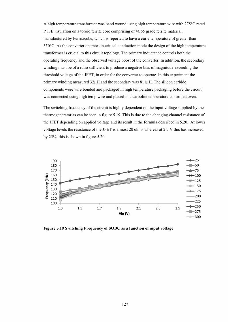
127
A high temperature transformer was hand wound using high temperature wire with 275°C rated
PTFE insulation on a toroid ferrite core comprising of 4C65 grade ferrite material,
manufactured by Ferroxcube, which is reported to have a curie temperature of greater than
350°C. As the converter operates in critical conduction mode the design of the high temperature
transformer is crucial to this circuit topology. The primary inductance controls both the
operating frequency and the observed voltage boost of the converter. In addition, the secondary
winding must be of a ratio sufficient to produce a negative bias of magnitude exceeding the
threshold voltage of the JFET, in order for the converter to operate. In this experiment the
primary winding measured 32µH and the secondary was 811µH. The silicon carbide
components were wire bonded and packaged in high temperature packaging before the circuit
was connected using high temp wire and placed in a carbolite temperature controlled oven.
The switching frequency of the circuit is highly dependent on the input voltage supplied by the
thermogenerator as can be seen in figure 5.19. This is due to the changing channel resistance of
the JFET depending on applied voltage and its result in the formula described in 5.20. At lower
voltage levels the resistance of the JFET is almost 20 ohms whereas at 2.5 V this has increased
by 25%, this is shown in figure 5.20.
Figure 5.19 Switching Frequency of SOBC as a function of input voltage
100
110
120
130
140
150
160
170
180
190
1.3 1.5 1.7 1.9 2.1 2.3 2.5
Fre
qu
en
cy (
kH
z)
Vin (V)
25
50
75
100
125
150
175
200
225
250
275
300

128
Figure 5.20 Rising JFET channel resistance with applied bias voltage
It can also be seen that the magnetic properties of the transformer core at elevated temperatures
also has an effect on frequency as can be seen in figure 5.21. This time the permeability of the
magnetic core increases with temperature, this has the effect of altering the inductance of both
the primary and secondary coils on the transformer causing them to both increase in magnitude,
but it can be seen that this effect is far less noticeable for any temperature than an increase in
Thermogenerator output voltage. It can be seen however the frequency decreases which is
linked to the reduced resistance values of the JFET which were extracted.
Figure 5.21 Variation in frequency dependant on Vin and temperature
0
5
10
15
20
25
30
0
0.02
0.04
0.06
0.08
0.1
0.12
1.3 1.5 1.7 1.9 2.1 2.3 2.5
Re
sist
an
ce (
Oh
ms)
Cu
rre
nt
(A)
Voltage (V)
Current
Resistance
100
110
120
130
140
150
160
170
180
190
25 75 125 175 225 275
Fre
qu
en
cy (
kH
z)
Temperature (C)
Vin = 1.3v
Vin = 1.4v
Vin = 1.5v
Vin = 1.6v
Vin = 1.7v
Vin = 1.8v
Vin = 1.9v
Vin = 2.0v
Vin = 2.1v
Vin = 2.2v
Vin = 2.3v
Vin = 2.4v
Vin = 2.5v

129
Despite the variation in frequency being dependant on both the input voltage and the magnetic
properties at elevated temperatures, the Self Oscillating boost converter continued to boost
voltages over the entire temperature range with a decrease performance at higher temperatures
due to the increase in resistance of devices as shown in figure 5.22.
Figure 5.22. Decreasing VOUT with increasing temperature
Figure 5.23. Shows the voltage conversion ratio of the boost converter at a range of
temperatures showing that even at 300 degrees Celsius the voltage boost is still over 2.5 times
the input voltage.
Figure 5.23. Voltage Conversion Ratio at different temperatures
Figure 5.24. shows the efficiency of the boost converter as a function of temperature it can be
quite clearly seen that the boost converter is more efficient at higher input voltages which also
3
4
5
6
7
8
9
10
25 75 125 175 225 275
Vo
ut
(V)
Temperature (C)
Vin = 1.3v
Vin = 1.4v
Vin = 1.5v
Vin = 1.6v
Vin = 1.7v
Vin = 1.8v
Vin = 1.9v
Vin = 2.0v
Vin = 2.1v
Vin = 2.2v
Vin = 2.3v
Vin = 2.4v
Vin = 2.5v
2.5
3
3.5
4
4.5
5
1.3 1.5 1.7 1.9 2.1 2.3 2.5
VC
R
Vin (V)
25
50
75
100
125
150
175
200
225
250
275
300

130
results in increased frequency of the circuit. Although the efficiency of the converter could be
viewed as low, one must take into account the nature of the devices available, the environment
in which they are placed and the simplicity of the circuit which requires no switching control.
Figure 5.24. Efficiency of the boost converter.
A drawback to this circuit design is the need for a large capacitor both to smooth the voltage
spikes caused by the boost circuit. Current Aluminium electrolytic capacitors in large values can
be purchased to operate at 200ºC but further research into high temperature energy storage is a
necessity for both DC/DC converters and energy storage.
5.7 Conclusions
In this chapter energy harvesting techniques to supply a high temperature SiC wireless sensor
node for perpetual operation have been explored. Thermoelectric devices were chosen as the
most appropriate energy harvesting technology due to the ambient high temperature
environment. A novel self oscillating boost converter topology has been demonstrated, and by
using a normally on SiC JFET it has been shown to increase voltages from a thermoelectric
device or other high current low voltage source to power further silicon carbide electronic
circuits.
The self oscillating boost converter was commissioned using a counter wound transformer on
high temperature ferrite, a SiC JFET and a SiC SBD. Based upon the operation of a free running
blocking oscillator, oscillatory behaviour is a result of the electric and magnetic variations in the
winding of the transformer and the amplification characteristics of a JFET. It demonstrated the
0
5
10
15
20
25
30
35
1.3 1.5 1.7 1.9 2.1 2.3 2.5
Eff
icie
ncy
%
Voltage In (V)
25 degrees
50 degrees
75 degrees
100 degrees
125 degrees
150 degrees
175 degrees
200 degrees
225 degrees
250 degrees
275 degrees
300 degrees

131
ability to boost an input voltage of 1.3 volts to 3.9 volts at 573K and exhibited an efficiency of
30% at room temperature. The frequency of operation was highly dependent upon the input
voltage due to the increased current flow through the primary coil portion of the transformer and
the ambient temperature causing an increase in permeability of the ferrite, thus altering the
inductance of both primary and secondary windings. However due its simplicity and its ability
to boost the input voltage by 250% meant it was capable of powering the transmitters and so
formed the basis for the power electronics of high temperature silicon carbide sensor node.
The addition of an RC network or controlling the resistance to the gate of the JFET can be used
to control the frequency of this self oscillating boost converter to some extent, but a more
thorough investigation into JFET based blocking oscillator theory obtained a novel
mathematical model and formula to describe the operation system based only upon the JFET
channel resistance and the relationship between inductors. As with the oscillators in the
previous chapter the extreme conditions and temperature range that silicon carbide electronics
can be subjected to, causes the electrical properties of all the components to change
dramatically, these effects cause frequency of any oscillator to vary and more complex circuits
are required for control.
5.8 References
[1] Status of silicon carbide (SiC) as a wide-bandgap semiconductor for high-temperature
applications: A review, J.B. Casady, R.W. Johnson, Solid-State Electronics, Volume 39, Issue
10, October 1996, Pages 1409–1422
[2] Silicon Carbide JFET Radiation Response, J.M. McGarrity, F.B. McLean, W.M. DeLancey,
J. Palmour, C. Carter, J. Edmond, R.E. Oakley IEEE Transactions on nuclear science, Vol. 39,
No. 6. December 1992
[3] William J. Nuttall, Nuclear Renaissance: Technologies and Policies for the Future of
Nuclear Power, 2004 CRC Press
[4] Bin Yang et al, Electromagnetic energy harvesting from vibrations of multiple frequencies,
J. Micromech. Microeng. 19 (2009) 035001 (8pp)
[5] Alper Erturk, Daniel J. Inman, Piezoelectric Energy Harvesting
[6] Nonlinear stochastic controllers for power-flow-constrained vibratory energy harvesters, Ian
L. Cassidy, Jeffrey T. Scruggs, Journal of Sound and Vibration, Volume 332, Issue 13, 24 June
2013, Pages 3134–3147
132
[7] High temperature vibration energy harvester system, Barker, S. Vassilevski, K.V. Wright,
N.G., Horsfall, A.B. IEEE SENSORS 2010
[8] S Barker, PhD Thesis, Newcastle University, 2011
[9] Precharging Piezo cantilever during operation [Paul Mitchell – Imperial] Try IEEE Sensors
2012 – Taiwan
[10] Solar cell efficiency tables (version 39) Martin A. Green, Keith Emery, Yoshihiro
Hishikawa, Wilhelm Warta and Ewan D. Dunlop, Prog. Photovolt: Res. Appl. 2012; 20:12–20
[11] 4H- and 6H-SiC UV photodetectors, Ludwig Östlund, Qin Wang*, Romain Esteve,
Susanne Almqvist, David Rihtnesberg, Sergey Reshanov, Andy Z. Z. Zhang, Jang-Kwon Lim,
Mietek Bakowski, Adolf Schöner, and Wlodek Kaplan, Phys. Status Solidi C 9, No. 7, 1680–
1682 (2012)
[12] Simon Barker et al, Silicon Carbide based Energy Harvesting Module for Hostile
Environments, Material Science Forum Vols 645-648 (2010) pp 1093-1096
[13] Witold Brostow, Gregory Granowski, Nathalie Hnatchuk, Jeff Sharp and John B. White,
Thermoelectric Phenomena, Journal of Materials Education Vol. 36 (5-6): 175 - 186 (2014)
[14] Complex thermoelectric materials, G. Jeffrey Snyder, Eric S. Toberer, Nature Materials 7,
105 - 114 (2008)
[15] http://chemgroups.northwestern.edu/kanatzidis/resources/BestZTs.jpg
[16] Art of Electronics, Horwitz and hill
[17] Christophe Basso, Switch-Mode Power Supplies Spice Simulations and Practical Designs
[18] www.maximintegrated.com/en/app-notes/index.mvp/id/4087
[19] Digitally Controlled Boost Power-Factor-Correction Converters Operating in Both
Continuous and Discontinuous Conduction Mode, Koen De Gussemé, David M. Van de Sype,
Alex P. M. Van den Bossche, Jan A. Melkebeek, IEEE Transactions on industrial electronics,
VOL. 52, NO. 1, Feb 2005
[20] Design Consideration for Power Factor Correction Boost Converter Operating at the
Boundary of Continuous Conduction Mode and Discontinuous Conduction Mode, Jih-Sheng
Lai, Daoshen Chen, Applied Power Electronics Conference and Exposition, 1993. APEC '93.
Conference Proceedings 1993., Eighth Annual
[21] Vaccum Valves in pulse technique, P.A. Neeteson, Phillips Technical Library
133
[22] P. Bhatnagar, A. B. Horsfall, N. G. Wright, C. M. Johnson, K. V. Vassilevski, A. G.
O´Neill, "Optimisation of a 4H-SiC enhancement mode power JFET for high temperature
operation" Solid-State Electronics, Vol. 49, Issue 3, March 2005, pp. 453-458
[23] Blocking Oscillators, R. Benjamin, IEEE VOL. 93. PART IIIA (RADIOLOCATION), NO.
7. 1946
[24] Comparison of basic converter topologies for power factor correction, H. Wei, I. Batarseh,
Southeastcon '98. Proceedings. IEEE
[25] Step-up DC-DC Converter With Coupled Inductors For Low Input Voltages, Markus
Pollak, Loreto Mateu, Peter Spies, Proceedings of PowerMEMS 2008+ microEMS 2008,
Sendai, Japan, November 9-12, (2008)
[26] Simplified Analysis of PWM Converters Using Model of PWM Switch Part II:
Discontinuous Conduction Mode, Vatche Vorperian, IEEE Transactions on Areospace and
Electronic Systems Vol. 24, No. 3 May 1990

134
Chapter 6: Conclusion
The work presented in this thesis has demonstrated the initial steps towards a high temperature
wireless sensor node constructed from SiC devices and high temperature passives, capable of
being powered using energy harvesting techniques. It has experimentally demonstrated both the
feasibility of wireless communication circuitry and a novel self oscillating boost converter
topology for powering silicon carbide circuitry within hostile environments
Depletion mode (normally on) JFETs have been characterised at temperatures up to 573K, and
parameters required to describe the JFET using SPICE ( TOV , β , λ , IS , RS and junction
capacitances) were extracted. These parameters allowed the mathematical description of the
operation of high temperature circuits. The transconductance of SiC JFETs at high temperatures
has been shown to decrease quadratically with increasing temperature, indicating a strong
dependence upon carrier mobility in the channel. The channel resistance also decreased
quadratically, as a direct result of both electric field and temperature enhanced trap emission.
The JFETs were shown to be operational at temperatures up to 775K, where they failed due to
delamination of an external passivation layer.
Schottky diodes have also been characterised at temperatures up to 573K and values for ideality
factor, depletion capacitance, series resistance and forward voltage drop were extracted to
mathematically model and simulate the devices. The series resistance of a SiC SBD exhibited a
quadratic increase with temperature, indicating that it is dominated by optical phonon scattering
of charge carriers in the epilayer. The observed deviation from a temperature independent
ideality factor is most likely due to the recombination of carriers in the depletion region and is
affected by both traps and the formation of an interfacial layer at the SiC/metal interface during
the fabrication. To compliment the silicon carbide active devices utilised in this work, high
temperature passive devices and packaging/circuit boards were explored and developed. AlN
and Al2O3 were identified as suitable high temperature packaging and circuit board substrates
along with gold as the most appropriate high temperature connective metal. Commercial surface
mount resistors fabricated from metallic oxides rated for 300°C were characterised above their
rating and both positive and negative temperature coefficients were observed. Despite these
temperature variations they were found to be both reliable and easily integrated into high
temperature SiC circuitry. Metallic spiral inductors for radio frequency oscillators were
fabricated from appropriately electroplated thickness of gold and were found to agree with the
relevant theoretical formula describing their changing attributes with regards to both resistance
and inductance at elevate temperatures.

135
HfO2 and AlN dielectrics have been investigated for use as potential high temperature capacitor
dielectrics in metal-insulator-metal (MIM) capacitor structures. The different thicknesses of
HfO2 (60nm and 90nm) and 300nm for AlN and the relevance to fabrication techniques were
examined and their effective capacitor behaviour at high temperature explored. The HfO2 based
capacitor structures exhibited high levels of leakage current at temperatures above 100°C,
especially for high electric fields, due to the thin dielectric and high defect density. This
rendered HfO2 unsuitable as the dielectric material in capacitors designed for operation in
hostile environments. To address this issue AlN capacitors with a greater dielectric film
thickness were fabricated with reduced leakage currents even at electric fields of 50MV/cm at a
temperature of 600K.
The work demonstrated the world’s first high temperature wireless sensor node powered using
energy harvesting technology, capable of operation at 573K. Two separate circuits were
commissioned and the results confirmed the operation of the world’s first amplitude modulation
(AM) and frequency modulation (FM) communication systems operating at high temperatures.
The AM oscillator circuitry operated at a maximum temperature of 553K, with a centre
frequency of 19.4MHz and a signal amplitude 65dBm above the background noise. Realised
from JFETs and HfO2 capacitors, modulation of the output signal was achieved by varying the
load resistance by use of a SiC JFET placed on the output. By applying a negative signal
voltage of between -2.5 and -3V, a 50% reduction in the signal amplitude was achieved.
Temperature Drift in the characteristics were also observed, with the resonant frequency
decreasing by almost 200 kHz when the temperature increased from 300K to 573K. This
decrease is linked to the increase in capacitance density of the HfO2 MIM capacitors and
increasing junction capacitances of the JFET used as the amplifier within the oscillator circuit.
Direct frequency modulation of a SiC Voltage Controlled Oscillator circuit was demonstrated at
a temperature of 573K, with a resonant frequency of 17MHz. The circuit was realised from a
SiC JFET, AlN capacitors and a SiC SBD used as a varactor. It was possible to vary the
frequency of oscillations by 100kHz with an input signal no greater than 1.5V being applied to
the SiC SBD. The effects of temperature drift were more dramatic in comparison to the AM
circuit at 400 KHz over the entire temperature range, a result of the properties of the AlN film
which causes the capacitors to increase in capacitance density by 10%.
An investigation in to the potential of using different energy harvesting techniques was
performed to determine the most appropriate technique for use in high temperature hostile
environments. Due to the elevated ambient temperatures and the technological maturity of
energy harvesting technologies, Thermoelectric generators were selected as the most
appropriate. A novel self oscillating boost converter topology has been developed and was
commissioned using a counter wound transformer on high temperature ferrite, a SiC JFET and a
SiC SBD. Based upon the operation of a free running blocking oscillator, oscillatory behaviour

136
is a result of the electric and magnetic variations in the winding of the transformer and the
amplification characteristics of a JFET. Designed to work with low voltage high current energy
harvesting devices such as thermoelectric generators and photovoltaics, it is capable of boosting
input voltages to a level sufficient to facilitate the operation of SiC circuits, such as the
oscillators and signal conditioning circuitry. Thus, this converter reduces the need for utilising
multiple energy harvesting devices connected electrically in series, reducing overall physical
dimensions of the system.
The converter demonstrated the ability to boost an input voltage of 1.3 volts to an output level
of 3.9 volts at 573K and exhibited an efficiency of 30% at room temperature. The frequency of
operation was highly dependent upon the input voltage due to the increased current flow
through the primary coil portion of the transformer and the ambient temperature causing an
increase in permeability of the ferrite, thus altering the inductance of both primary and
secondary windings. However due its simplicity and its ability to boost the input voltage by
250% meant it was capable of powering the transmitters and so formed the basis for a self
powered high temperature silicon carbide sensor node.
The demonstration of these high temperature circuits have provided the initial stages of being
able to produce a high temperature wireless sensor node capable of operation in hostile
environments whilst harvesting energy from the high temperature ambient. Along with
appropriate sensor technology it demonstrated the feasibility of being able to monitor and
transmit information from hazardous locations which is currently unachievable.
6.1 Future Work
Silicon carbide technology has the potential to operate effectively in high temperature and
radioactive hostile environments. Currently the majority of research is aimed at improving
substrate quality and utilising SiC properties to manufacture power devices for energy saving
purposes in a variety of applications, from electrical power distribution to electric vehicles. The
improvements in substrate quality has a direct impact on the development of silicon carbide
technology. The growth of more uniform wafers with fewer defects will ultimately allow for
more reliable and complex circuitry to be fabricated. As silicon carbide technology grows and
matures with its major partner (GaN and the solid state lighting industry) prices will drop
allowing for more high performance components to be commercially viable. Although there has
been minimal research conducted into signal level devices, the properties of silicon carbide can
be harnessed to create extremely resilient electronics suitable for a multitude of purposes. Many
of the developments and lessons learnt through the fabrication of traditional silicon technology

137
can be applied directly to the fabrication of SiC devices. These discoveries may increase the
speed at which silicon carbide integrated circuitry develops.
Self powered wireless sensor nodes fabricated from silicon carbide still face multiple challenges
which have been touched upon in this thesis. Integrated circuitry whether built from MESFET,
JFET or MOSFET technologies has the potential to greatly increase circuit complexity,
allowing for more developed oscillators and control mechanisms. This will allow for greater
control over frequency drift with temperature resulting from both physical changes within SiC
and its passive counter parts.
Analogue circuitry such as amplifiers and high temperature voltage reference circuits needs
further research, so that the different polytypes of silicon carbide and other high temperature
sensors can be more effectively monitored. The fabrication of digital electronic circuits also
requires more research and development and although results in the literature have shown that it
is possible to create a range simple digital circuits such as gates and flip-flops, substrate quality
and price are two of the main factors which restrict further advances at the current time.
Through the research conducted into digital technologies we can expect a far greater complexity
and functionality of SiC circuitry, including enhanced energy management circuits along with
ultimately analogue to digital converters and microprocessors, thus allowing for a digital
representation of the analogue world from the analogue sensor inputs and the corresponding
transmission of this digital data.
Packaging technology for extreme environments is an area which is often overlooked and needs
additional research. In particular there currently a gap in the commercial market for high
temperature solders and die attach materials. The majority of solder will not withstand
temperatures above 300°C, as it is above its melting point. In contrast, high temperature
precious metal solders have melting points of 550°C and beyond. In conjunction with this
problem, high temperature soldering equipment must also be investigated as its maximum
melting temperature is below precious metal solders. Research and development into the
printing of circuit board traces may prove to be more cost effective when utilising precious
metals as traces, in the traditional methods of etching or milling unwanted metal from PCBs in
not viable due to large costs. PCB substrates will need to be investigated although AlN and
Al2O3 appear good candidates for both IC packaging and PCBs the materials as fragile and can
crack as a direct result of thermal stresses.
Capacitor technology remains a critical area in need of significant development, although small
value capacitors for high temperatures can be manufactured through the techniques in this work
and there are commercial entities which provide such high temperature capacitors. There are no
large value capacitors or known technology to fabricate such devices; this has severe limitations
in power handling and storage circuits. When harvesting energy in any environment it can often

138
only be acquired sporadically, for example when it is sunny, windy, hot, and as a result a
capacitor technology is required to store this energy for intermittent use by the system load thus
allowing a module to operate over periods of time when no energy can be harvested. Increased
capacitance density is also required for high temperature SiC power converter technologies all
converter technologies produce voltage ripple which have to be smoothed and regulated by a
large capacitor.
Battery technology for use in high temperature environment is also an area in need of further
research wireless sensors nodes with the addition of a high temperature battery for backup
purposes are extremely desirable. Although there are high temperature batteries commercially
available based on molten salts they have a minimum temperature operation limitation. As they
are only able to operate at high temperatures this may prove problematic as some hostile
environments may have a much greater variation in temperature ranging from 30 – 600°C in the
case of a combustion engine for example.
Energy harvesting for silicon electronics is still in its infancy, at higher temperatures there a
multiple other problems such as capacitor and battery technologies to also be considered.
However, more research is required into SiC photovoltaic’s and high temperature materials both
for the construction of TEG’s and Piezoelectric devices. Also overlooked is in cyclical changes
in temperature a piezoelectric crystal will generate electricity from expansion and contraction
without the need for vibration.
Although there are many research questions to address, the properties and potential of silicon
carbide electronics ensures great promise in the future.