silicon based integrated optical switching technology for ... · 1 shigeru nakamura green platform...
TRANSCRIPT

1
Shigeru Nakamura
Green Platform Res. Labs., NEC Corporation
Silicon based integrated optical switching technology for telecom application
Oct. 22, 2013 ISUPT 2013
Page 2
Outline
・Application to optical path switches for next generation ROADMUltrafast network currently being upgraded will enable and also requireoptical layer flexibility with optical path switches.
・Our approach to optical switches with silicon photonics
・Demonstration on optical switch circuitsbased on silicon photonics device integration

2
Page 3
・Application to optical path switchesfor next generation ROADM
Page 4
Evolution toward next generation CDC-ROADM
Conventional ROADM Next generation ROADM
Static connection betweentransponders and lines
Transponders
AWGMany transpondersfor advancedmodulation format
"Optical switching"
Reconfigurable or dynamic connectionbetween transponders and lines
- Color-less- Direction-less- Contention-less
Higher flexibilityin optical layer
ROADM: Reconfigurable Optical Add Drop Multiplexer
2-degreetransmissionlines
Multi-degreetransmission lines
(CDC)

3
Page 5
CDC-ROADMs
• Any transponders can be used for setting up path at any wavelength for any direction.
• Each transponder can be used for multiple purposes. Multiple transponders can be used for single purpose.
• Increase in transponder usage efficiency. Reduction in transponder number.• Shared backup scheme leading to highly reliable and cost-effective failure recovery• Higher reconfigurability corresponding to unexpected traffic change
Configuration Functions
Colorless
…
λ1~λx
…
…
Directionless
λ1
…
λ2 λx
…
λ1
…
λ1 λ1λ1
ContentionlessCut-through partwith WSS
Transponder aggregatorpart
Benefitsl-tunabletransponders
Transmissionlines
Page 6
Several proposals for transponder aggregator
l-tunable transponders
Transponder aggregator part
Transmission lines
Cyclic AWG
Splitter Splitter Splitter Splitter Splitter Splitter Splitter Splitter
Selector Selector Selector Selector Selector Selector Selector Selector
K. Mizutani , M. Sakauchi and A. Tajima,ECOC2010 P3.11 (2010).
Cycl ic AWG
Cut-through part with WSS
Configuration of CDC-ROADM
Examples of transponder aggregator using silica waveguide devices
T. Watanabe, K. Suzuki, T. Goh, K. Hattori,A. Mori, T. Takahashi, T. Sakamoto, K. Morita,S. Sohma, S. Kamei, OFC2011 OTuD3 (2011).
Cy cli c AWG
Cy clic AWG
Contention-less
Direction-less
Color-less
Split & Select AWG & Matrix Switch

4
Page 7
Ultra-compact optical switch based on silicon photonics
l-tunabletransponders
Transmission lines
Configuration of CDC-ROADM
Transponder aggregator
WSS
Splitter Selector
Splitter Selector
Splitter Selector
Splitter Selector
Splitter Selector
Splitter Selector
Splitter Selector
Splitter Selector
8x8 split & select switch
Si ribwaveguide
Heater
Electrodepads
100 um
Input
Output(Bar port)
Output(Cross port)
Mach-Zehnder TO switch element
Si coreSiO2 cladding
Sharply bendedwaveguide
Efficient thermo-optical effect
Heating
Si core
Page 8
Optical switch
Electrical path switch
Opticaltransponder
IP router
Electrical packet switch
Server゙ Storage゙LAN
Server゙ Storage゙
Rooter・Switch
LAN
Data center
Wide area network
Home user
Business user
Rooter・Switch
Data center
Optical network node
AccessMobile backhaul
Higher network flexibilitycoping with unexpected traffic change or failure and being provided with low power consumption is a basic requirement.
Optical fiber
Optical switch providesflexibility or reconfigurabilityin the lowest layerwith the lowest power consumption
Many effort in many layerstoward improvement of flexibility
Basic expectation for optical switch
5
Page 9
・Our approach to optical switcheswith silicon photonics
Page 10
Silicon photonics
Conventionaldiscreteoptical devices
Large silicon wafer
Optical switch Optical transceiverSilicon photonics
Switchingelement
AWG Photo-detector
Modulator
Cost effectively developinghigh density, large scale optical device integration
- Ultra-small, low-power optical devices- Design rules for their integration- Use of sophisticated CMOS process

6
Page 11
SiO2 core Dimension: 5~7 um
Conventional SiO2 waveguide
SiO2 cladding Large core dimensionSmall index contrastWeak light confinementGentle waveguide bending (Curvature radius: 1~10 mm)
Si waveguide
Si core Dimension: 0.3~1 umSiO2 cladding Small core dimension
Large index contrastStrong light confinementSharp waveguide bending(Curvature radius: 10~100 um)
10~50mm
100~500mm
Comparison of AWG size
Ultra-small optical devices using Si waveguidesStrong light confinement into small core with high index contrast,thus sharp waveguide bending
Page 12
NW equipment IT equipment
Cost 1/10
Optical path switchfor wide area network
Optical transceiverfor interconnect
2cm0.25mm
3cm 1~10Tb/s
LSI
Size 1/10 Power 1/10
Chip-to-chip/on-chipoptical interconnect
What generation of process technology is applied?
Small volume Large volume
Silicon photonics application
Rakesh Kumar, "Fabless Semiconductor Implementation," 2008
Si CMOSProcess technology
Progress under Moore's law

7
Page 13
Selecting waveguide structure compatible with process
1 um
10 um
100 um
1 mm
10 mm
100 mm
1 um
10 um
100 um
1 mm
10 mm
100 mm
0.01 dB/cm
0.1 dB/cm
1 dB/cm
10 dB/cm
100 dB/cm
0.01 dB/cm
0.1 dB/cm
1 dB/cm
10 dB/cm
100 dB/cm
0.1 um
Ben
ding
Rad
ius
Pro
paga
tion
Loss
1 um 10 umWaveguide width
SiON SiO2Si-RibSi-Wire Loss∝σ2/d4
Si sub.
SiO2 cladding
Ge-SiO2 core
5~7 umSi sub.
Si rib core
SiO2 cladding
Si sub.
Si wire core
SiO2 cladding
Fluctuation~10nm
Fluctuation~4nm
Si CMOS process technologyParameters representing size fluctuation・Roughness・Uniformity
Si waveguide technologySize fluctuation influences waveguide properties・Propagation loss・Polarization dependence・Phase error in interference devices
Loss s2/d4130nm
2001
90nm
2004
65nm
2007
45nm
2010
32nm
2013
22nm
2016
DRAM Half pitch
Crit
ical
dim
ensi
on U
nifo
rmity
(nm
)R
ough
ness
3s
(nm
)
1
10
100
130nm
2001
90nm
2004
65nm
2007
45nm
2010
32nm
2013
22nm
2016
DRAM Half pitch
Crit
ical
dim
ensi
on U
nifo
rmity
(nm
)R
ough
ness
3s
(nm
)
1
10
100
Page 14
Option in silicon optical waveguide cross section
Si sub.
Si wire core
0.2~0.5mm
Si sub.
Si ribSiO2 cladding
Si sub.
Si rib
21
22
21
2nnn
Refractiveindexcontrast
~1.5mm~5mm
40%5%1%Contrast of effective refractive indexes at rib and slab
10%
10
0.1
1
Opt
ical
dev
ice
size
(mm
)
SiO2 cladding SiO2 cladding
8
Page 15
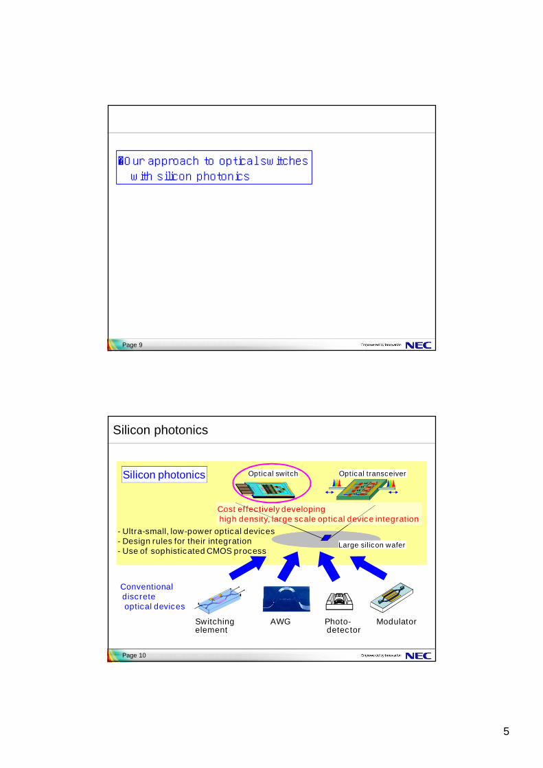
AWG: Arrayed waveguide grating
TE
TM
Polarization independence
500 um
1575 1580 1585 1590 1595 1600 1605-60
-50
-40
-30
-20
-10
Tran
smis
sion
(dB)
Wavelength (nm)
-: TE-: TM
Optical spectraStructure
Input Output
Si rib waveguide
Si sub.
Si rib
~1.5mm
SiO2 cladding
8 inch wafer
248-nm lithography process
Page 16
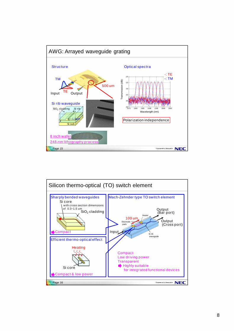
Si ribwaveguide
Heater
Electrodepads
Silicon thermo-optical (TO) switch element
Si corewith cross section dimensionsof 0.3~1.5 um
SiO2 cladding
Heating
Si core
100 um
Input
Output(Bar port)
Output(Cross port)
Sharply bended waveguides
Efficient thermo-optical effect
Mach-Zehnder type TO switch element
Compact
Compact & low power
CompactLow driving powerTransparent
Highly suitablefor integrated functional devices

9
Page 17
-60
-50
-40
-30
-20
0 20 40 60 80 100
Tran
smis
sion
(dB
)
Power (mW)
Basic properties of Si TO switch element
0 20 40 60 80 1000.0
0.5
1.0
Inte
nsity
(a.u
.)
Time (ms)
~ 13 ms
0 20 40 60 80 1000.0
0.5
1.0
Inte
nsity
(a.u
.)
Time (ms)
~ 14 ms
100 um
TE
TM
Input
Output(Bar port)
Output on-off contrast
Time response
Switching time ~ 15 us
Easily controllableCross state without heatingBar state with heating
Polarization independence
Structure
Output(Cross port)
Si ribwaveguide
Heater
Electrodepads
Si rib waveguide
Bar port
Cross port
~25 dB
Si sub.
Si rib
~1.5mm
SiO2 cladding
8 inch wafer
248-nm lithography process
Page 18
・Demonstration on optical switch circuitsbased on silicon photonics device integration

10
Page 19
Silicon optical switch using split & select configuration
Silicon optical circuitincluding 152 switch elementsis formed within the areaof 16 x 12 mm.
1 x 8 selector switch
Gate part Selector part
Splitter Selector
Splitter Selector
Splitter Selector
Splitter Selector
Splitter Selector
Splitter Selector
Splitter Selector
Splitter Selector
8 x 8 split & select switch
TO switch element
Si ribwaveguide
Heater
Electrodepads
100 um
Requirements
- Small footprint- Low power- Low loss- Polarization independent- Wide wavelength range- High on-off contrast- Ambient temperature independent- ...
Page 20
Light propagation in silicon TO switch element
Constructiveat cross port
Destructiveat bar port
Ambient temperature insensitiveMach-Zehnder is symmetric.Without heating one arm
Destructiveat cross port
Constructiveat bar portIndex increase
Ambient temperature sensitive
With heating one arm
11
Page 21
Temperature characteristics of Si TO switch element
G. Cocorullo, F. G. Della Corte, and I. Rendina,Appl. Phys. Lett. vol. 74, pp. 3338 - 3340 (1999).
Temperature dependenceof Si thermo-optic coefficient (dn/dT)
RIdTdn
RV
dTdnP
dTdnT
dTdnn 2
2
Temperature dependenceof heater resistance (R)
R
Temp.
Refractive index change in Si when heated
Underconstantvoltage
Underconstantcurrent
Mach-Zehnder is symmetric, the arm lengths of Mach-Zehnder are the same.We still need to consider temp. characteristics when one arm is heated.
Page 22
Measured temperature characteristicsOutput (Bar port)
-30
-20
-10
0
10
0 20 40 60 80 100
Tran
smis
sion
(dB
)
Power (mW)
-30
-20
-10
0
10
2.7 2.8 2.9 3 3.1 3.2
Tran
smis
sion
(dB
)
Voltage (V)
-30
-20
-10
0
10
4 4.1 4.2 4.3 4.4 4.5
Tran
smis
sion
(dB
)
Voltage (V)
-30
-20
-10
0
10
11.5 12 12.5 13 13.5 14
Tran
smis
sion
(dB
)
Current (mA)
-30
-20
-10
0
10
16.5 17 17.5 18 18.5 19
Tran
smis
sion
(dB
)
Current (mA)
-:75C-:50C-:25C-: 0C
Si ribwaveguide
Heater
Electrodepads
100 um
Input
Output(Bar port)
Output(Cross port)
As a function of heater power
As a function of heater current
As a function of heater voltage

12
Page 23
Light propagation in silicon TO switch element
Constructiveat cross port
Destructiveat bar port
Ambient temperature insensitiveMach-Zehnder is symmetric.Without heating one arm
Destructiveat cross port
Constructiveat bar portIndex increase
Ambient temperature sensitiveparticularly when constant current drive is used.
With heating one arm
Page 24
1 x 8 selector switch part
Gate part Selector part
Configuration of 1 x 8 selector switch
1 mm
1 m
m
Adding gate part and using configuration that light blocking is doneby two-stage gate elements, 1x8 selector switch part becomes tolerantto ambient temperature change

13
Page 25
Temperature independent, high extinction switching
1570 1580 1590 1600 1610 1620-90
-80
-70
-60
-50
-40
-30
-20 Filename: 110927-1F01->F05,F07 : 110927C1-C4,D1-D4
Tran
smis
sion
(dB
)
Wavelength (nm)1570 1580 1590 1600 1610 1620
-100
-90
-80
-70
-60
-50
-40
-30
Tran
smis
sion
(dB
)
Wavelength (nm)
-:TE-:TM -:75C
-:50C-:25C-: 0C
Measured transmission spectra showing on-off contrast
For different polarization
40dB 40dB
High extinction ratio (>40 dB)Wide wavelength range (>50 nm)Polarization independentAmbient temperature independent under constant current drive
At different ambient temperature
S. Nakamura, S. Takahashi, I. Ogura, J. Ushida, K. Kurata, T. Hino, H. Takeshita, A. Tajima, M.-B. Yu, and G.-Q. Lo, OFC2012, OTu2I.3 (2012).
Page 26
Splitter Selector
Splitter Selector
Splitter Selector
Splitter Selector
Splitter Selector
Splitter Selector
Splitter Selector
Splitter Selector
Toward silicon optical switch module
1 x 8 selector switch
Gate part Selector part
8 x 8 split & select switch 8x8 optical paths can beset up using 152 TO MZswitch elements, whichare integrated in the areaof 12 mm x 16 mm.
Optical switch circuit part Opticalin/out part
Silicon optical switch chipOptical fiber array
M. Tokushima, et al., Appl. Phys. Express vol. 5, 022202, (2012).

14
Page 27
Conclusion
Silicon thermo-optical switch element
Integration of silicon thermo-optical switchestoward next generation ROADMs
Using a devised configuration of 1 x 8 selector switch, high extinction, temperature independent optical switching is achieved.
8 x 8 split & select type optical switch- Small & Low power- Polarization independent (less than 0.8 dB)- Wide wavelength range (over 50 nm)- High on-off contrast (over 40-45 dB)- Ambient temperature independent (over the range of 0 - 75 C)- Low loss
Internal loss excluding splitter loss (less than 5 dB)Coupling loss - In progress
- Packaging - Near future