si4720-21-b20 data sheet
TRANSCRIPT

Rev. 1.0 2/08 Copyright © 2008 by Silicon Laboratories Si4720/21-B20.
Si4720/21-B20
BROADCAST FM RADIO TRANSCEIVER FOR PORTABLE APPLICATIONS
Features
Applications
Description
The Si4720/21 integrates the complete tuner and transmit functions forFM broadcast reception and standards-compliant, unlicensed FMbroadcast stereo transmission. Users must comply with local radiofrequency (RF) transmission regulations.
Functional Block Diagram
Full FM RX and TX in 3 x 3 QFN
Worldwide FM RX band support
Compliant with worldwide FM TX regulations
Excellent real-world performance
Supports integrated TX/RX antenna
Programmable transmit output voltage
Frequency synthesizer with integrated VCO
Integrated LDO regulator
Minimal BOM (15 mm2)
Digital audio output(Si4721 only)
Digital audio input
Adjustable seek parameters
Adjustable mono/stereo blend
Adjustable soft mute
Advanced modulation control
Audio dynamic range control
Audio silence detector
Programmable reference clock input
2-wire and 3-wire control interface
2.7 to 5.5 V supply voltage
3 x 3 x 0.55 mm 20-pin Pb-free QFN package
RDS/RDBS encoder/decoder(Si4721 only)
Cellular handsets/hands-free
MP3 players
Portable media players
Wireless speakers/microphone
Satellite digital audio radios
Personal computers/notebooks
ADC
ADC
Si4720/21
DSP
DAC
DAC
PGA
AFC
MU
X
FMI
AGC
Tx/Rx Ant
Rx Ant*
TXO
RFGND
RC
LK VIO
SCLK
SDIO
CONTROLINTERFACE
SEN
GPO
GPO
3/D
CLK
RST
GPO
2/IN
T
LIN/DFS
RIN/DOUT
ROUT/DIN
LOUT/DFS
GPO
1
LDO
VDD
GND
2.7–5.5 V
C122 uF
L1120 nH
LNA
*Note: Dedicated Rx antenna is optional
Patents pending
Notes:1. To ensure proper operation and FM
transceiver performance, follow the guidelines in “AN383: 3 mm x 3 mm QFN Universal Layout Guide.” Silicon Laboratories will evaluate schematics and layouts for qualified customers.
2. Place the Si4720/21 as close as possible to the antenna jack, and keep the FMI trace as short as possible.
Ordering Information:
See page 42.
Pin Assignments
GNDPAD
1
2
3
17181920
11
12
13
14
6 7 8 9
4
5
16
10
15
GPO
2/IN
T
VIO
RIN/DOUT
LOUT/DFS
ROUT/DIN
GNDRST
NC
TXO
RC
LK
SDIO
VDD
FMI
RFGND
GPO
3/D
CLK
NC
GPO
1
LIN
/DFS
SCLK
SEN
Si4720/21(Top View)

Si4720/21-B20
2 Rev. 1.0
Si4720/21-B20
Rev. 1.0 3
TABLE OF CONTENTS
Section Page
1. Electrical Specifications . . . . . . . . . . . . . . . . . . . . . . . . . . . . . . . . . . . . . . . . . . . . . . . . . . .52. Test Circuit . . . . . . . . . . . . . . . . . . . . . . . . . . . . . . . . . . . . . . . . . . . . . . . . . . . . . . . . . . . . .19
2.1. Test Circuit Schematic . . . . . . . . . . . . . . . . . . . . . . . . . . . . . . . . . . . . . . . . . . . . . . .192.2. Test Circuit Bill of Materials . . . . . . . . . . . . . . . . . . . . . . . . . . . . . . . . . . . . . . . . . . . .19
3. Typical Application Schematic . . . . . . . . . . . . . . . . . . . . . . . . . . . . . . . . . . . . . . . . . . . . .203.1. Analog Audio Inputs/Outputs . . . . . . . . . . . . . . . . . . . . . . . . . . . . . . . . . . . . . . . . . .203.2. Typical Application Bill of Materials . . . . . . . . . . . . . . . . . . . . . . . . . . . . . . . . . . . . . .203.3. Digital Audio Inputs/Outputs . . . . . . . . . . . . . . . . . . . . . . . . . . . . . . . . . . . . . . . . . . .213.4. Typical Application Schematic Bill of Materials . . . . . . . . . . . . . . . . . . . . . . . . . . . . .21
4. Universal AM/FM RX/FM TX Application Schematic . . . . . . . . . . . . . . . . . . . . . . . . . . . .224.1. Universal AM/FM RX/FM TX Bill of Materials . . . . . . . . . . . . . . . . . . . . . . . . . . . . . .23
5. Functional Description . . . . . . . . . . . . . . . . . . . . . . . . . . . . . . . . . . . . . . . . . . . . . . . . . . .245.1. Overview . . . . . . . . . . . . . . . . . . . . . . . . . . . . . . . . . . . . . . . . . . . . . . . . . . . . . . . . . .245.2. Application Schematics and Operating Modes . . . . . . . . . . . . . . . . . . . . . . . . . . . . .255.3. FM Receiver . . . . . . . . . . . . . . . . . . . . . . . . . . . . . . . . . . . . . . . . . . . . . . . . . . . . . . .255.4. Integrated Antenna Support . . . . . . . . . . . . . . . . . . . . . . . . . . . . . . . . . . . . . . . . . . .265.5. Receiver Digital Audio Interface (Si4721 Only) . . . . . . . . . . . . . . . . . . . . . . . . . . . . .265.6. Stereo Audio Processing . . . . . . . . . . . . . . . . . . . . . . . . . . . . . . . . . . . . . . . . . . . . . .275.7. De-emphasis . . . . . . . . . . . . . . . . . . . . . . . . . . . . . . . . . . . . . . . . . . . . . . . . . . . . . . .285.8. Stereo DAC . . . . . . . . . . . . . . . . . . . . . . . . . . . . . . . . . . . . . . . . . . . . . . . . . . . . . . . .285.9. Soft Mute . . . . . . . . . . . . . . . . . . . . . . . . . . . . . . . . . . . . . . . . . . . . . . . . . . . . . . . . . .285.10. RDS/RBDS Processor (Si4721 Only) . . . . . . . . . . . . . . . . . . . . . . . . . . . . . . . . . . .285.11. Tuning . . . . . . . . . . . . . . . . . . . . . . . . . . . . . . . . . . . . . . . . . . . . . . . . . . . . . . . . . . .285.12. Seek . . . . . . . . . . . . . . . . . . . . . . . . . . . . . . . . . . . . . . . . . . . . . . . . . . . . . . . . . . . .285.13. Reference Clock . . . . . . . . . . . . . . . . . . . . . . . . . . . . . . . . . . . . . . . . . . . . . . . . . . .285.14. FM Transmitter . . . . . . . . . . . . . . . . . . . . . . . . . . . . . . . . . . . . . . . . . . . . . . . . . . . .295.15. Receive Power Scan . . . . . . . . . . . . . . . . . . . . . . . . . . . . . . . . . . . . . . . . . . . . . . . .295.16. Transmitter Digital Audio Interface . . . . . . . . . . . . . . . . . . . . . . . . . . . . . . . . . . . . .305.17. Line Input . . . . . . . . . . . . . . . . . . . . . . . . . . . . . . . . . . . . . . . . . . . . . . . . . . . . . . . .315.18. Audio Dynamic Range Control . . . . . . . . . . . . . . . . . . . . . . . . . . . . . . . . . . . . . . . .325.19. Audio Limiter . . . . . . . . . . . . . . . . . . . . . . . . . . . . . . . . . . . . . . . . . . . . . . . . . . . . . .335.20. Pre-emphasis and De-emphasis . . . . . . . . . . . . . . . . . . . . . . . . . . . . . . . . . . . . . . .335.21. RDS/RBDS Processor (Si4721 Only) . . . . . . . . . . . . . . . . . . . . . . . . . . . . . . . . . . .335.22. Tuning . . . . . . . . . . . . . . . . . . . . . . . . . . . . . . . . . . . . . . . . . . . . . . . . . . . . . . . . . . .335.23. Reference Clock . . . . . . . . . . . . . . . . . . . . . . . . . . . . . . . . . . . . . . . . . . . . . . . . . . .335.24. Control Interface . . . . . . . . . . . . . . . . . . . . . . . . . . . . . . . . . . . . . . . . . . . . . . . . . . .335.25. GPO Outputs . . . . . . . . . . . . . . . . . . . . . . . . . . . . . . . . . . . . . . . . . . . . . . . . . . . . . .355.26. Reset, Powerup, and Powerdown . . . . . . . . . . . . . . . . . . . . . . . . . . . . . . . . . . . . . .355.27. Programming with Commands . . . . . . . . . . . . . . . . . . . . . . . . . . . . . . . . . . . . . . . .35
6. Commands and Properties . . . . . . . . . . . . . . . . . . . . . . . . . . . . . . . . . . . . . . . . . . . . . . . .367. Pin Descriptions: Si4720/21-GM . . . . . . . . . . . . . . . . . . . . . . . . . . . . . . . . . . . . . . . . . . . .41
Si4720/21-B20
4 Rev. 1.0
8. Ordering Guide . . . . . . . . . . . . . . . . . . . . . . . . . . . . . . . . . . . . . . . . . . . . . . . . . . . . . . . . . .429. Package Markings (Top Marks) . . . . . . . . . . . . . . . . . . . . . . . . . . . . . . . . . . . . . . . . . . . . .43
9.1. Top Mark Explanation . . . . . . . . . . . . . . . . . . . . . . . . . . . . . . . . . . . . . . . . . . . . . . . .439.2. Si4720/21 Top Mark . . . . . . . . . . . . . . . . . . . . . . . . . . . . . . . . . . . . . . . . . . . . . . . . .439.3. Si4721 Top Mark . . . . . . . . . . . . . . . . . . . . . . . . . . . . . . . . . . . . . . . . . . . . . . . . . . . .43
10. Package Outline: Si4720/21-GM . . . . . . . . . . . . . . . . . . . . . . . . . . . . . . . . . . . . . . . . . . .4411. PCB Land Pattern: Si4720/21-GM . . . . . . . . . . . . . . . . . . . . . . . . . . . . . . . . . . . . . . . . . .4512. Additional Reference Resources . . . . . . . . . . . . . . . . . . . . . . . . . . . . . . . . . . . . . . . . . .47Contact Information . . . . . . . . . . . . . . . . . . . . . . . . . . . . . . . . . . . . . . . . . . . . . . . . . . . . . . . .48
Si4720/21-B20
Rev. 1.0 5
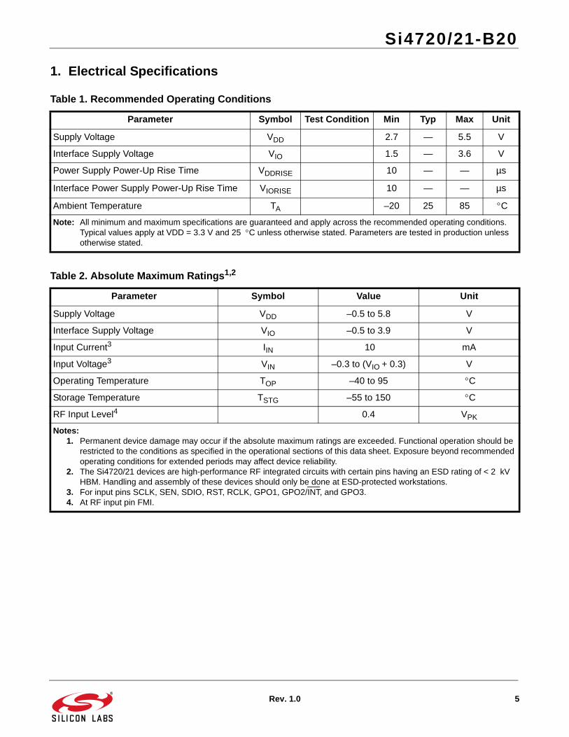
1. Electrical Specifications
Table 1. Recommended Operating Conditions
Parameter Symbol Test Condition Min Typ Max Unit
Supply Voltage VDD 2.7 — 5.5 V
Interface Supply Voltage VIO 1.5 — 3.6 V
Power Supply Power-Up Rise Time VDDRISE 10 — — µs
Interface Power Supply Power-Up Rise Time VIORISE 10 — — µs
Ambient Temperature TA –20 25 85 C
Note: All minimum and maximum specifications are guaranteed and apply across the recommended operating conditions. Typical values apply at VDD = 3.3 V and 25 C unless otherwise stated. Parameters are tested in production unless otherwise stated.
Table 2. Absolute Maximum Ratings1,2
Parameter Symbol Value Unit
Supply Voltage VDD –0.5 to 5.8 V
Interface Supply Voltage VIO –0.5 to 3.9 V
Input Current3 IIN 10 mA
Input Voltage3 VIN –0.3 to (VIO + 0.3) V
Operating Temperature TOP –40 to 95 C
Storage Temperature TSTG –55 to 150 C
RF Input Level4 0.4 VPK
Notes:1. Permanent device damage may occur if the absolute maximum ratings are exceeded. Functional operation should be
restricted to the conditions as specified in the operational sections of this data sheet. Exposure beyond recommended operating conditions for extended periods may affect device reliability.
2. The Si4720/21 devices are high-performance RF integrated circuits with certain pins having an ESD rating of < 2 kV HBM. Handling and assembly of these devices should only be done at ESD-protected workstations.
3. For input pins SCLK, SEN, SDIO, RST, RCLK, GPO1, GPO2/INT, and GPO3.4. At RF input pin FMI.

Si4720/21-B20
6 Rev. 1.0
Table 3. DC Characteristics
Parameter Symbol Test Condition Min Typ Max Unit
FM Receiver
RX Supply Current IRX — 19.2 22 mA
RX Supply Current1 IRX Low SNR level — 19.8 23 mA
RX Interface Supply Current IIORX — 320 600 µA
RX RDS Supply Current2 IFM Analog Output Mode — 19.9 23 mA
RX Supply Current2 IFMD Digital Output Mode — 18.0 20.5 mA
FM Transmitter
TX Supply Current ITX — 18.8 22.8 mA
TX Interface Supply Current IIOTX — 320 600 µA
FM Transmitter from Digital Audio Input
TX Supply Current IDTX DCLK = 3.072 MHz — 18.3 — mA
TX Interface Supply Current IDIO DCLK = 3.072 MHz — 320 — µA
FM Transmitter in Receive Power Scan Mode
RX Supply Current IRX — 16.8 — mA
RX Interface Supply Current IIORPS — 400 — µA
Supplies and Interface
VDD Powerdown Current IDDPD Powerdown mode — 10 20 µA
VIO Powerdown Current IIOPD SCLK, RCLK inactivePowerdown mode
— 3 10 µA
High Level Input Voltage3 VIH 0.7 x VIO — VIO + 0.3 V
Low Level Input Voltage3 VIL –0.3 — 0.3 x VIO V
High Level Input Current3 IIH VIN = VIO = 3.6 V –10 — 10 µA
Low Level Input Current3 IIL VIN = 0 V, VIO = 3.6 V –10 — 10 µA
High Level Output Voltage4 VOH IOUT = 500 µA 0.8 x VIO — — V
Low Level Output Voltage4 VOL IOUT = –500 µA — — 0.2 x VIO V
Notes:1. LNA is automatically switched to higher current mode for optimum sensitivity in weak signal conditions.2. Guaranteed by characterization.3. For input pins SCLK, SEN, SDIO, RST, RCLK, GPO1, GPO2/INT, and GPO3.4. For output pins SDIO, GPO1, GPO2/INT, and GPO3.

Si4720/21-B20
Rev. 1.0 7
Figure 1. Reset Timing Parameters for Busmode Select
Table 4. Reset Timing Characteristics1,2,3
(VDD = 2.7 to 5.5 V, VIO = 1.5 to 3.6 V, TA = –20 to 85 °C)
Parameter Symbol Min Typ Max Unit
RST Pulse Width and GPO1, GPO2/INT Setup to RST tSRST 100 — — µs
GPO1, GPO2/INT Hold from RST tHRST 30 — — ns
Important Notes:1. When selecting 2-wire mode, the user must ensure that a 2-wire start condition (falling edge of SDIO while SCLK is
high) does not occur within 300 ns before the rising edge of RST.2. When selecting 2-wire mode, the user must ensure that SCLK is high during the rising edge of RST, and stays high until
after the 1st start condition.3. When selecting 3-wire or SPI modes, the user must ensure that a rising edge of SCLK does not occur within 300 ns
before the rising edge of RST.4. If GPO1 and GPO2 are actively driven by the user, then minimum tSRST is only 30 ns. If GPO1 or GPO2 is hi-Z, then
minimum tSRST is 100 µs, to provide time for on-chip 1 M devices (active while RST is low) to pull GPO1 high and GPO2 low.
70%
30%
GPO170%
30%
GPO2/INT
70%
30%
tSRST
RST
tHRST

Si4720/21-B20
8 Rev. 1.0
Table 5. 2-Wire Control Interface Characteristics1,2,3
(VDD = 2.7 to 5.5 V, VIO = 1.5 to 3.6 V, TA = –20 to 85 °C)
Parameter Symbol Test Condition Min Typ Max Unit
SCLK Frequency fSCL 0 — 400 kHz
SCLK Low Time tLOW 1.3 — — µs
SCLK High Time tHIGH 0.6 — — µs
SCLK Input to SDIO Setup (START)
tSU:STA 0.6 — — µs
SCLK Input to SDIO Hold (START) tHD:STA 0.6 — — µs
SDIO Input to SCLK Setup tSU:DAT 100 — — ns
SDIO Input to SCLK Hold4,5 tHD:DAT 0 — 900 ns
SCLK input to SDIO Setup (STOP) tSU:STO 0.6 — — µs
STOP to START Time tBUF 1.3 — — µs
SDIO Output Fall Time tf:OUT — 250 ns
SDIO Input, SCLK Rise/Fall Time tf:INtr:IN
— 300 ns
SCLK, SDIO Capacitive Loading Cb — — 50 pF
Input Filter Pulse Suppression tSP — — 50 ns
Notes:1. When VIO = 0 V, SCLK and SDIO are low-impedance. 2-wire control interface is I2C compatible.2. When selecting 2-wire mode, the user must ensure that a 2-wire start condition (falling edge of SDIO while SCLK is
high) does not occur within 300 ns before the rising edge of RST.3. When selecting 2-wire mode, the user must ensure that SCLK is high during the rising edge of RST, and stays high
until after the first start condition.4. The Si4720/21 delays SDIO by a minimum of 300 ns from the VIH threshold of SCLK to comply with the minimum
tHD:DAT specification.5. The maximum tHD:DAT has only to be met when fSCL = 400 kHz. At frequencies below 400 KHz, tHD:DAT may be
violated as long as all other timing parameters are met.
20 0.1Cb
1 pF------------+
20 0.1Cb
1 pF------------+

Si4720/21-B20
Rev. 1.0 9
Figure 2. 2-Wire Control Interface Read and Write Timing Parameters
Figure 3. 2-Wire Control Interface Read and Write Timing Diagram
SCLK70%
30%
SDIO70%
30%
START STARTSTOP
tf:INtr:INtLOW tHIGHtHD:STAtSU:STA tSU:STOtSP tBUF
tSU:DATtr:INtHD:DAT
tf:IN,
tf:OUT
SCLK
SDIO
START STOPADDRESS + R/W ACK DATA ACK DATA ACK
A6-A0, R/W
D7-D0 D7-D0

Si4720/21-B20
10 Rev. 1.0
Figure 4. 3-Wire Control Interface Write Timing Parameters
Figure 5. 3-Wire Control Interface Read Timing Parameters
Table 6. 3-Wire Control Interface Characteristics(VDD = 2.7 to 5.5 V, VIO = 1.5 to 3.6 V, TA = –20 to 85 °C)
Parameter Symbol Test Condition Min Typ Max Unit
SCLK Frequency fCLK 0 — 2.5 MHz
SCLK High Time tHIGH 25 — — ns
SCLK Low Time tLOW 25 — — ns
SDIO Input, SEN to SCLKSetup tS 20 — — ns
SDIO Input to SCLKHold tHSDIO 10 — — ns
SEN Input to SCLKHold tHSEN 10 — — ns
SCLKto SDIO Output Valid tCDV Read 2 — 25 ns
SCLKto SDIO Output High Z tCDZ Read 2 — 25 ns
SCLK, SEN, SDIO, Rise/Fall time tR, tF — — 10 ns
Note: When selecting 3-wire mode, the user must ensure that a rising edge of SCLK does not occur within 300 ns before the rising edge of RST.
SCLK70%
30%
SEN70%
30%
SDIO A7 A070%
30%
tS
tS
tHSDIO tHSEN
A6-A5,R/W,
A4-A1
Address In Data In
D15 D14-D1 D0
tHIGH tLOW
tR tF
½ Cycle Bus Turnaround
SCLK70%
30%
SEN70%
30%
SDIO70%
30%
tHSDIO tCDVtCDZ
Address In Data Out
A7 A0A6-A5,R/W,
A4-A1D15 D14-D1 D0
tS
tS tHSEN

Si4720/21-B20
Rev. 1.0 11
Figure 6. SPI Control Interface Write Timing Parameters
Figure 7. SPI Control Interface Read Timing Parameters
Table 7. SPI Control Interface Characteristics(VDD = 2.7 to 5.5 V, VIO = 1.5 to 3.6 V, TA = –20 to 85 °C)
Parameter Symbol Test Condition Min Typ Max Unit
SCLK Frequency fCLK 0 — 2.5 MHz
SCLK High Time tHIGH 25 — — ns
SCLK Low Time tLOW 25 — — ns
SDIO Input, SEN to SCLKSetup tS 15 — — ns
SDIO Input to SCLKHold tHSDIO 10 — — ns
SEN Input to SCLKHold tHSEN 5 — — ns
SCLKto SDIO Output Valid tCDV Read 2 — 25 ns
SCLKto SDIO Output High Z tCDZ Read 2 — 25 ns
SCLK, SEN, SDIO, Rise/Fall time tR, tF — — 10 ns
Note: When selecting SPI mode, the user must ensure that a rising edge of SCLK does not occur within 300 ns before the rising edge of RST.
SCLK70%
30%
SEN70%
30%
SDIO C7 C070%
30%
tS
C6–C1
Control Byte In 8 Data Bytes In
D7 D6–D1 D0
tS
tHSDIOtHIGH tLOWtHSEN
tFtR
Bus Turnaround
SCLK70%
30%
SEN70%
30%
SDIO 70%
30%
tHSDIO
Control Byte In
C7 C0C6–C1
tS tHSEN
tS
tCDZ
tCDV
16 Data Bytes Out(SDIO or GPO1)
D7 D6–D1 D0

Si4720/21-B20
12 Rev. 1.0
Figure 8. Digital Audio Interface Timing Parameters, I2S Mode
Table 8. Digital Audio Interface Characteristics (Receive)(VDD = 2.7 to 5.5 V, VIO = 1.5 to 3.6 V, TA = –20 to 85 °C)
Parameter Symbol Test Condition Min Typ Max Unit
DCLK Cycle Time tDCT 26 — 1000 ns
DCLK pulse width high tDCH 10 — — ns
DCLK pulse width low tDCL 10 — — ns
DFS set-up time to DCLK rising edge tSU:DFS 5 — — ns
DFS hold time from DCLK rising edge tHD:DFS 5 — — ns
DOUT propagation delay from DCLK falling edge tPD:DOUT 0 — 12 ns
DCLK
DFS
tDCT
tPD:OUT
tSU:DFStHD:DFS
DOUT
tDCH tDCL

Si4720/21-B20
Rev. 1.0 13
Table 9. FM Receiver Characteristics1,2
(VDD = 2.7 to 5.5 V, VIO = 1.5 to 3.6 V, TA = –20 to 85 °C)
Parameter Symbol Test Condition Min Typ Max Unit
Input Frequency fRF 76 — 108 MHz
Sensitivity with Headphone Net-work3,4,5
(S+N)/N = 26 dB — 2.2 3.5 µV EMF
Sensitivity with 50 Network3,4,5,6 (S+N)/N = 26 dB — 1.1 — µV EMF
RDS Sensitivity6 f = 2 kHz, RDS BLER < 5%
— 15 — µV EMF
TXO Receiver Mode Sensitivity6 — 3.5 — µV EMF
LNA Input Resistance6,7 3 4 5 k
LNA Input Capacitance6,7 4 5 6 pF
Input IP36,8 100 105 — dBµV EMF
AM Suppression3,4,6,7 m = 0.3 40 50 — dB
Adjacent Channel Selectivity ±200 kHz 35 50 — dB
Alternate Channel Selectivity ±400 kHz 60 70 — dB
Spurious Response Rejection6 In-band 35 — — dB
Audio Output Voltage3,4,7 72 80 90 mVRMS
Audio Output L/R Imbalance3,7,9 — — 1 dB
Audio Frequency Response Low6 –3 dB — — 30 Hz
Audio Frequency Response High6 –3 dB 15 — — kHz
Audio Stereo Separation7,9 25 — — dB
Audio Mono S/N3,4,5,7,10 55 63 — dB
Audio Stereo S/N4,5,7,10,11 — 58 — dB
Audio THD3,7,9 — 0.1 0.5 %
De-emphasis Time Constant6 FM_DEEMPHASIS = 2 70 75 80 µs
FM_DEEMPHASIS = 1 45 50 54 µs
Audio Output Load Resistance6,10 RL Single-ended 10 — — k
Notes:1. Additional testing information is available in Application Note AN388. Volume = maximum for all tests. Tested at
RF = 98.1 MHz.2. To ensure proper operation and receiver performance, follow the guidelines in “AN383: Antenna Selection and
Universal Layout Guidelines.” Silicon Laboratories will evaluate schematics and layouts for qualified customers.3. FMOD = 1 kHz, 75 µs de-emphasis, MONO = enabled, and L = R unless noted otherwise.4. f = 22.5 kHz.5. BAF = 300 Hz to 15 kHz, A-weighted.6. Guaranteed by characterization.7. VEMF = 1 mV.8. |f2 – f1| > 2 MHz, f0 = 2 x f1 – f2. AGC is disabled. Refer to "7. Pin Descriptions: Si4720/21-GM" on page 41. 9. f = 75 kHz.10. At LOUT and ROUT pins.11. Analog audio output mode.12. At temperature 25 °C.

Si4720/21-B20
14 Rev. 1.0
Audio Output Load Capacitance6,10 CL Single-ended — — 50 pF
Seek/Tune Time6 RCLK tolerance = 100 ppm
— — 80 ms/channel
Powerup Time6 From powerdown — — 110 ms
RSSI Offset12 Input levels of 8 and 60 dBµV at RF Input
–3 — 3 dB
Table 9. FM Receiver Characteristics1,2 (Continued)(VDD = 2.7 to 5.5 V, VIO = 1.5 to 3.6 V, TA = –20 to 85 °C)
Parameter Symbol Test Condition Min Typ Max Unit
Notes:1. Additional testing information is available in Application Note AN388. Volume = maximum for all tests. Tested at
RF = 98.1 MHz.2. To ensure proper operation and receiver performance, follow the guidelines in “AN383: Antenna Selection and
Universal Layout Guidelines.” Silicon Laboratories will evaluate schematics and layouts for qualified customers.3. FMOD = 1 kHz, 75 µs de-emphasis, MONO = enabled, and L = R unless noted otherwise.4. f = 22.5 kHz.5. BAF = 300 Hz to 15 kHz, A-weighted.6. Guaranteed by characterization.7. VEMF = 1 mV.8. |f2 – f1| > 2 MHz, f0 = 2 x f1 – f2. AGC is disabled. Refer to "7. Pin Descriptions: Si4720/21-GM" on page 41. 9. f = 75 kHz.10. At LOUT and ROUT pins.11. Analog audio output mode.12. At temperature 25 °C.

Si4720/21-B20
Rev. 1.0 15
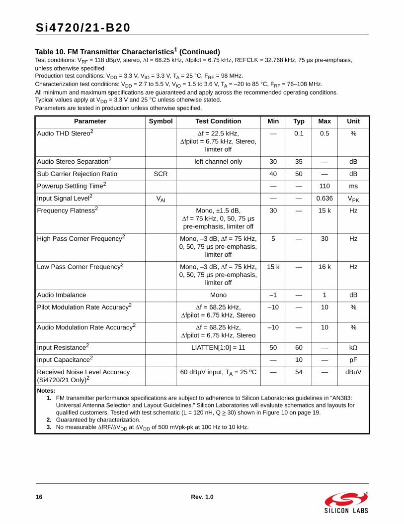
Table 10. FM Transmitter Characteristics1
Test conditions: VRF = 118 dBµV, stereo, f = 68.25 kHz, fpilot = 6.75 kHz, REFCLK = 32.768 kHz, 75 µs pre-emphasis,
unless otherwise specified.Production test conditions: VDD = 3.3 V, VIO = 3.3 V, TA = 25 °C, FRF = 98 MHz.
Characterization test conditions: VDD = 2.7 to 5.5 V, VIO = 1.5 to 3.6 V, TA = –20 to 85 °C, FRF = 76–108 MHz.
All minimum and maximum specifications are guaranteed and apply across the recommended operating conditions.Typical values apply at VDD = 3.3 V and 25 °C unless otherwise stated.
Parameters are tested in production unless otherwise specified.
Parameter Symbol Test Condition Min Typ Max Unit
Transmit Frequency Range2 fRF 76 — 108 MHz
Transmit Frequency Accuracy and Stability2,3
–3.5 — 3.5 kHz
Transmit Voltage Accuracy2 VRF = 103–117 dBµV –2.5 — 2.5 dB
Transmit Voltage Accuracy VRF = 102, 118 dBµV –2.5 — 2.5 dB
Transmit Voltage Temperature Coef-ficient2
–0.075 — –0.025 dB/°C
Transmit Channel Edge Power > ±100 kHz, pre-emphasis off
— — –20 dBc
Transmit Adjacent Channel Power > ±200 kHz, pre-emphasis off
— –30 –26 dBc
Transmit Alternate Channel Power > ±400 kHz, pre-emphasis off
— –30 –26 dBc
Transmit Emissions In-band (76–108 MHz) — — –30 dBc
Output Capacitance Max2 CTUNE — 53 — pF
Output Capacitance Min2 CTUNE — 5 — pF
Pre-emphasis Time Constant2 TX_PREMPHASIS = 75 µs 70 75 80 µs
TX_PREMPHASIS = 50 µs 45 50 54 µs
Audio SNR Mono2 f = 22.5 kHz, Mono, limiter off
58 63 — dB
Audio SNR Stereo f = 22.5 kHz, fpilot = 6.75 kHz, Stereo,
limiter off
53 58 — dB
Audio THD Mono f = 75 kHz, Mono, limiter off
— 0.1 0.5 %
Notes:1. FM transmitter performance specifications are subject to adherence to Silicon Laboratories guidelines in “AN383:
Universal Antenna Selection and Layout Guidelines.” Silicon Laboratories will evaluate schematics and layouts for qualified customers. Tested with test schematic (L = 120 nH, Q > 30) shown in Figure 10 on page 19.
2. Guaranteed by characterization.3. No measurable fRF/VDD at VDD of 500 mVpk-pk at 100 Hz to 10 kHz.
Si4720/21-B20
16 Rev. 1.0
Audio THD Stereo2 f = 22.5 kHz, fpilot = 6.75 kHz, Stereo,
limiter off
— 0.1 0.5 %
Audio Stereo Separation2 left channel only 30 35 — dB
Sub Carrier Rejection Ratio SCR 40 50 — dB
Powerup Settling Time2 — — 110 ms
Input Signal Level2 VAI — — 0.636 VPK
Frequency Flatness2 Mono, ±1.5 dB, f = 75 kHz, 0, 50, 75 µs pre-emphasis, limiter off
30 — 15 k Hz
High Pass Corner Frequency2 Mono, –3 dB, f = 75 kHz, 0, 50, 75 µs pre-emphasis,
limiter off
5 — 30 Hz
Low Pass Corner Frequency2 Mono, –3 dB, f = 75 kHz, 0, 50, 75 µs pre-emphasis,
limiter off
15 k — 16 k Hz
Audio Imbalance Mono –1 — 1 dB
Pilot Modulation Rate Accuracy2 f = 68.25 kHz, fpilot = 6.75 kHz, Stereo
–10 — 10 %
Audio Modulation Rate Accuracy2 f = 68.25 kHz, fpilot = 6.75 kHz, Stereo
–10 — 10 %
Input Resistance2 LIATTEN[1:0] = 11 50 60 — k
Input Capacitance2 — 10 — pF
Received Noise Level Accuracy (Si4720/21 Only)2
60 dBµV input, TA = 25 ºC — 54 — dBuV
Table 10. FM Transmitter Characteristics1 (Continued)Test conditions: VRF = 118 dBµV, stereo, f = 68.25 kHz, fpilot = 6.75 kHz, REFCLK = 32.768 kHz, 75 µs pre-emphasis,
unless otherwise specified.Production test conditions: VDD = 3.3 V, VIO = 3.3 V, TA = 25 °C, FRF = 98 MHz.
Characterization test conditions: VDD = 2.7 to 5.5 V, VIO = 1.5 to 3.6 V, TA = –20 to 85 °C, FRF = 76–108 MHz.
All minimum and maximum specifications are guaranteed and apply across the recommended operating conditions.Typical values apply at VDD = 3.3 V and 25 °C unless otherwise stated.
Parameters are tested in production unless otherwise specified.
Parameter Symbol Test Condition Min Typ Max Unit
Notes:1. FM transmitter performance specifications are subject to adherence to Silicon Laboratories guidelines in “AN383:
Universal Antenna Selection and Layout Guidelines.” Silicon Laboratories will evaluate schematics and layouts for qualified customers. Tested with test schematic (L = 120 nH, Q > 30) shown in Figure 10 on page 19.
2. Guaranteed by characterization.3. No measurable fRF/VDD at VDD of 500 mVpk-pk at 100 Hz to 10 kHz.

Si4720/21-B20
Rev. 1.0 17
Figure 9. Digital Audio Interface Timing Parameters, I2S Mode
Table 11. Digital Audio Interface Characteristics (Transmit)(VDD = 2.7 to 5.5 V, VIO = 1.5 to 3.6 V, TA = –20 to 85 °C)
Parameter Symbol Test Condition Min Typ Max Unit
DCLK pulse width high tDCH 10 — — ns
DCLK pulse width low tDCL 10 — — ns
DFS set-up time to DCLK rising edge tSU:DFS 5 — — ns
DFS hold time from DCLK rising edge tHD:DFS 5 — — ns
DIN set-up time from DCLK rising edge tSU:DIN 5 — — ns
DIN hold time from DCLK rising edge tHD:DIN 5 — — ns
DCLK, DFS, DIN, Rise/Fall timetRtF
— — 10 ns
DCLK Tx Frequency1,2 1.0 — 40.0 MHz
Notes:1. Guaranteed by characterization.2. The DCLK frequency may be set below the minimum specification if DIGITAL_INPUT_SAMPLE_RATE is first set to 0
(disable).
DCLK
DFS
DINtSU:DIN
tSU:DFS
tHD:DIN
tHD:DFS
tFtR
Si4720/21-B20
18 Rev. 1.0
Table 12. FM Receive Power Scan Characteristics1
(VDD = 2.7 to 5.5 V, VIO = 1.5 to 3.6 V, TA = –20 to 85 °C, FRF = 76–108 MHz)
Parameter Symbol Test Condition Min Typ Max Unit
Tune and Signal Strength Measurement Time per Channel2
— — 80 ms
Notes:1. Settling time for ac coupling capacitors on the audio input pins after Receive to Transmit transition can take a few
hundred milliseconds. The actual settling time depends on the values of the ac-coupling capacitors. Using digital audio input mode avoids this settling time.
2. Guaranteed by characterization.
Table 13. Reference Clock and Crystal Characteristics(VDD = 2.7 to 5.5 V, VIO = 1.5 to 3.6 V, TA = –20 to 85 °C)
Parameter Symbol Test Condition Min Typ Max Unit
Reference Clock
RCLK Supported Frequencies1 31.130 32.768 40,000 kHz
RCLK Frequency Tolerance2 –50 — 50 ppm
REFCLK_PRESCALE 1 — 4095
REFCLK 31.130 32.768 34.406 kHz
Crystal Oscillator
Crystal Oscillator Frequency — 32.768 — kHz
Crystal Frequency Tolerance2 –100 — 100 ppm
Board Capacitance — — 3.5 pF
Notes:1. The Si4720/21 divides the RCLK input by REFCLK_PRESCALE to obtain REFCLK. There are some RCLK
frequencies between 31.130 kHz and 40 MHz that are not supported. See “AN332: Si4704/05/06/1x/2x/3x/4x FM Transmitter/AM/FM/SW/LW/WB Receiver Programming Guide” for more details.
2. A frequency tolerance of ±50 ppm is required for FM seek/tune using 50 kHz channel spacing.
Si4720/21-B20
Rev. 1.0 19
2. Test Circuit
2.1. Test Circuit Schematic
Figure 10. Test Circuit Schematic
2.2. Test Circuit Bill of Materials
Table 14. Si4720/21 Test Circuit Bill of Materials
Component(s) Value/Description Supplier(s)
C1 Supply bypass capacitor, 22 nF, 20%, Z5U/X7R Murata
C2, C3 AC Coupling Capacitor, 0.47 µF Murata
C4 2 pF, ±.05 pF, 06035JZR0AB AVX
C5, C6 Crystal load capacitors, 22 pF, ±5%, COG(Optional: for crystal oscillator option)
Venkel
L1 120 nH inductor, Qmin = 30 Murata
R1 49.9 , 5% Murata
X1 32.768 kHz crystal (Optional: for crystal oscillator option) Epson
U1 Si4720/21 FM Radio Transceiver Silicon Laboratories
0.47 µF
0.47 µF
C4
R1
20 19 18 17 16
U1Si4720/21
NC
FMI
RFGND
TXO
RST
RIN
LOUT
ROUT
GND
VDD
NC
GPO
1
GPO
2/IN
T
GPO
3
LIN
SEN
SCLK
SDIO
RC
LK
V IO
SEN
SCLK
SDIO
1
2
3
4
5
15
14
13
12
11
6 7 8 9 10
RST
RCLK
C1VBATTERY2.7 to 5.5 V
VIO
1.5 to 3.6 V
LIN
RIN
TX Antenna
L12 pF
22 nF
VIO
50
VTXOUT
C2
C3
Notes:1. Si4720/21 is shown configured in I2C compatible bus mode.2. GPO2/INT can be configured for interrupts with the powerup command.3. To ensure proper operation and FM transmitter performance, follow the guidelines in “AN383: 3 mm x 3 mm QFN Universal Layout Guide.” Silicon Laboratories will evaluate schematics and layouts for qualified customers.4. LIN, RIN line inputs must be ac-coupled.
LOUTFMI
ROUT
120 nH
C5 C6
X1RCLK

Si4720/21-B20
20 Rev. 1.0
3. Typical Application Schematic
3.1. Analog Audio Inputs/Outputs
Figure 11. Analog Audio Inputs/Outputs (LIN, RIN, LOUT, ROUT)
3.2. Typical Application Bill of Materials
Table 15. Si4720/21 Typical Application Bill of Materials
Component(s) Value/Description Supplier(s)
C1 Supply bypass capacitor, 22 nF, 20%, Z5U/X7R Murata
C2, C3 AC Coupling Capacitor, 0.47 µF Murata
C4, C5 Crystal load capacitors, 22 pF, ±5%, COG(Optional: for crystal oscillator option)
Venkel
L1 120 nH inductor, Qmin = 30 Murata
X1 32.768 kHz crystal (Optional: for crystal oscillator option) Epson
U1 Si4720/21 FM Radio Transceiver Silicon Laboratories
20 19 18 17 16
U1Si4720/21
NC
FMI
RFGND
TXO
RST
RIN
LOUT
ROUT
GND
VDDN
C
GPO
1
GPO
2/IN
T
GPO
3
LIN
SEN
SCLK
SDIO
RC
LK
V IO
SEN
SCLK
SDIO
1
2
3
4
5
15
14
13
12
116 7 8 9 10
RST
RCLK
C1VBATTERY2.7 to 5.5 V
VIO
1.5 to 3.6 V
LIN
RIN
TX/RX Antenna
L1120 nH
22 nF
VIO C2
C3
0.47 µF
0.47 µF
Notes:1. Si4720/21 is shown configured in I2C compatible bus mode.2. GPO2/INT can be configured for interrupts with the powerup command.3. To ensure proper operation and FM transmitter performance, follow the guidelines in “AN383: 3 mm x 3 mm QFN Universal Layout Guide.” Silicon Laboratories will evaluate schematics and layouts for qualified customers.4. LIN, RIN line inputs must be ac-coupled.5. Dedicated RX antenna at FMI input optional.
LOUT
ROUT
C4 C5
X1RCLK
RX Antenna

Si4720/21-B20
Rev. 1.0 21
3.3. Digital Audio Inputs/Outputs
Figure 12. Digital Audio Inputs (DIN, DFS, DCLK)
3.4. Typical Application Schematic Bill of Materials
Table 16. Si4720/21 Bill of Materials
Component(s) Value/Description Supplier(s)
C1 Supply bypass capacitor, 22 nF, 20%, Z5U/X7R Murata
C2, C3 AC Coupling Capacitor, 0.47 µF Murata
L1 120 nH inductor, Qmin = 30 Murata
R1, R2 2 k Resistor Any
R3 600 Resistor Any
U1 Si4720/21 FM Radio Transceiver Silicon Laboratories
20 19 18 17 16
U1Si4720/21
NC
FMI
RFGND
TXO
RST
DOUT
DFS
DIN
GND
VDD
NC
GPO
1
GPO
2/IN
T
GPO
3/D
CLK
DFS
SEN
SCLK
SDIO
RC
LK
V IO
SEN
SCLK
SDIO
1
2
3
4
5
15
14
13
12
11
6 7 8 9 10
RST
RCLK
C1
DIN
VBATTERY2.7 to 5.5 V
VIO
1.5 to 3.6 V
DCLK
DFS
TX/RX Antenna
L1120 nH
22 nF
VIO
Notes:1. Si4720/21 is shown configured in I2C compatible bus mode.2. GPO2/INT can be configured for interrupts with the powerup command.3. To ensure proper operation and FM transmitter performance, follow the guidelines in “AN383: Si47xx 3 mm x 3 mm QFN Universal Layout Guide.” Silicon Laboratories will evaluate schematics and layouts for qualified customers.4. Dedicated RX antenna at FMI input optional.
R1
R2
R3
DOUT
DFS
RX Antenna

Si4720/21-B20
22 Rev. 1.0
4. Universal AM/FM RX/FM TX Application Schematic
Figure 13 shows an application schematic that supports the Si47xx family of 3 mm x 3 mm QFN products,including the Si4702/3/4/5 FM receivers, Si471x FM transmitters, Si472x FM transceivers, and Si473x AM/FMreceivers.
Figure 13. Universal AM/FM RX/FM TX Application Schematic
Following the schematic and layout recommendations detailed in “AN383: Universal Antenna Selection and LayoutGuidelines” will result in optimal performance with the minimal application schematic shown in Figure 13. “UniversalAM/FM RX/FM TX Application Schematic”. System components are those that are likely to be present for any tuneror transmitter design.
C41 nF
LHEADPHONE
270 nH
System Component
20 19 18 17 16U1
Si47xx
NC
FMI
RFGND
TXO/AMI
RST
GND/RIN/DOUT
LOUT/DFS
ROUT/DIN
GND
VDD
NC
GPO
1
GPO
2/IR
Q
GPO
3/D
CLK
LIN
/DFS
SEN
SCLK
SDIO
RC
LK
V IO
1
2
3
4
5
15
14
13
12
11
6 7 8 9 10
C1
VBATTERY2.7 to 5.5 V
LIN
LSHORT
120 nH
22 nF
R120
GPIO1
GPIO3GPIO2 R13
0
VBATTERY2.7 to 5.5 V
Si4702/03: Populate R12, R13, R21, C14, and C15Si4704/05/1x/2x/3x Analog: Populate C7, C8, C14 and C15 as shownSi4704/05/1x/2x/3x Digital: Populate R16, R17, R18, R19, and R20 as shown
C14/R190.39 uF/ 0
SEN
SCLK
SDIO
RST
RCLK
VIO
C15/R200.39 uF/ 0
C7/R170.39 uF/ 2 k
RIN
C8/R180.39 uF/ 600
System Components
C17/R213.3pF/0
LFERRITE
180–600 uH
FB12.5 k @ 100 MHz
FB22.5 k @ 100 MHz
HP JackJ1
S 1
R 2
T 5
RightAudio
LeftAudio
U2Headphone Amplifier
System Component
R140
R162 k
C16470 nF
FM Embedded RX/TX Antenna
AM Ferrite AntennaSystem Component
L110 nH
System Component
D5
D4D3
Si4720/21-B20
Rev. 1.0 23
4.1. Universal AM/FM RX/FM TX Bill of MaterialsThe bill of materials for the expanded application schematic shown in Figure 13 is provided in Table 17. Refer tothe individual device layout guides and antenna interface guides for a discussion of the purpose of eachcomponent.
Table 17. Universal AM/FM/RX/FM TX Bill of Materials
Designator Description Note
C1 Supply bypass capacitor, 22 nF, 10%, Z5U/X7R, 0402
U1 Silicon Laboratories Si47xx, 3 mm x 3 mm, 20 pin, QFN
R12, R13, R19, R20, R21
0 jumper, 0402 R12, R13, and R21 for Si4702/03 Only
C16 AM antenna ac coupling capacitor, 470 nF, 20%, Z5U/X7R AM Ferrite Antenna
LFERRITE AM Ferrite loop stick, 180–600 µH AM Ferrite Antenna
FB1,FB2 Ferrite bead, 2.5 k @ 100 MHZ, 0603, Murata BLM18BD252SN1D Headphone Antenna
LHEADPHONE Headphone antenna matching inductor, 270 nH, 0603, Q>15, Murata LQW18ANR27J00D
Headphone Antenna
LSHORT Embedded antenna matching inductor, 120 nH, 0603, Q>30, Murata LQW18ANR12J00D
Embedded Antenna
R14 Embedded antenna jumper, 2.2 , 0402 Optional
C2 Supply bypass capacitor, 22 nF, 10%, Z5U/X7R, 0402 Optional
C3 Supply bypass capacitor, 100 nF, 10%, Z5U/X7R, 0402 Optional
C5, C6 Headphone amp output shunt capacitor, 100 pF, 10%, Z5U/X7R, 0402 Optional
R7-R11 Current limiting resistor, 20 –2 k, 0402 Optional
C12, C13 Crystal load capacitor, 22 pF, 5%, COG Optional
X1 Crystal, Epson FC-135 Optional
C7, C8 Si47xx input ac coupling capacitor, 0.39 µF, X7R/X5R, 0402 System Component
D1-D5 ESD Diode, SOT23-3, California Micro Devices CM1214-01ST System Component
C11 Supply bypass capacitor, 100 nF, 10%, Z5U/X7R, 0402 Headphone Amplifier
C4 Headphone antenna ac coupling capacitor, 1 nF, 10%, Z5U/X7R, 0402 Headphone Antenna
C9, C10 Headphone amp output ac coupling capacitor, 125 uF, X7R, 0805 Headphone Amplifier
C14, C15 Headphone amp input ac coupling capacitor, 0.39 µF, X7R/X5R, 0402 Headphone Amplifier
R1,R2,R3,R4 Headphone amp feedback/gain resistor, 20 k, 0402 Headphone Amplifier
R5, R6 Headphone amp bleed resistor, 100 k, 0402 Headphone Amplifier
U2 Headphone amplifier, National Semiconductor, LM4910MA Headphone Amplifier
R16, R17 Current limiting resistor, 2 k0402 System Component
R18 Current limiting resistor, 600 , 0402 System Component
L1 VCO filter inductor, 10 nH, 0603, Q30, Murata, LQW18ANR01J00D Optional
C17 VCO filter capacitor, 3.3 pF, 0402, COG, Venkel, C0402COG2503R3JN
Optional
Si4720/21-B20
24 Rev. 1.0
5. Functional Description
5.1. Overview
Figure 14. Functional Block Diagram
The Si4720/21 is the first single-chip FM radiotransceiver. The proven and patented digitalarchitecture of the Si4720/21 combines the functionalityof the Si470x FM radio receiver with the Si471x FMtransmitter, offering full FM receive and transmitcapabilities in a single, ultra-small 3x3x0.55 mm QFNpackage. The device leverages Silicon Laboratories’highly successful and proven FM technology and offersunmatched integration and performance. FM receiverand transmit functionality may be added to any portabledevice by using this single chip. As with the Si470x andSi471x products, the Si4720/21 offers industry leadingsize, performance, low power consumption, and ease ofuse.
The Si4720/21 is the first FM radio transceiverintegrated circuit to support a small loop antenna, whichcan be integrated into the enclosure or PCB of aportable device. This feature enables applications thatalso include Bluetooth functionality to perform FM radioreception without cables. For portable navigationdevices, the Si4720’s antenna architecture permitsintegration of the traffic messaging antenna into theenclosure of the portable device, and eliminates theneed for external antenna cables.
The Si4720's digital integration reduces the requiredexternal components of traditional offerings, resulting ina solution requiring only an external inductor and
bypass capacitor, and a PCB space of approximately15 mm2. The Si4720/21 is layout compatible withSilicon Laboratories' Si470x FM radio receivers, Si473xAM/FM radio receivers, and the Si471x FM radiotransmitter solutions, allowing a single PCB layout toaccommodate a variety of music features. High yieldmanufacturability, unmatched performance, easydesign-in, and software programmability are keyadvantages of the Si4720.
The Si4720/21’s integrated receive power scan functionshares the same antenna as the transmitter allowing fora compact printed circuit board design. The deviceoperates in half duplex mode, meaning the transmitterand receiver do not operate at the same time.
The Si4720/21 performs FM modulation in the digitaldomain to achieve high fidelity, optimal performanceversus power consumption, and flexibility of design. Theonboard DSP provides modulation adjustment andaudio dynamic range control for optimum sound quality.
The Si4721 supports the European Radio Data System(RDS) and the US Radio Broadcast Data System(RBDS) including all the symbol encoding, blocksynchronization, and error correction functions. Usingthis feature, the Si4721 enables data such as artistname and song title to be transmitted to an RDS/RBDSreceiver.
ADC
ADC
Si4720
DSP
DAC
DAC
PGA
AFC
MU
X
FMI
AGC
Tx/Rx Ant
Rx Ant*
TXO
RFGND
RC
LK VIO
SCLK
SDIO
CONTROLINTERFACE
SEN
GPO
GPO
3
RST
GPO
2/IN
T
LIN
RIN
ROUT
LOUT
GPO
1
LDO
VDD
GND
2.7–5.5 V
C122 uF
L1120 nH
LNA
*Note: Dedicated Rx antenna is optional

Si4720/21-B20
Rev. 1.0 25
The transmit output (TXO) connects directly to thetransmit antenna with only one external inductor toprovide harmonic filtering. The output is programmableover a 10 dB voltage range in 1 dB steps. The TXOoutput pin can also be configured for loop antennasupport. Users are responsible for complying with localregulations on RF transmission (FCC, ETSI, ARIB,etc.).
The digital audio interface operates in slave mode andsupports a variety of MSB-first audio data formatsincluding I2S and left-justified modes. The interface hasthree pins: digital data input (DIN), digital framesynchronization input (DFS), and a digital bitsynchronization input clock (DCLK). The Si4720/21supports a number of industry-standard sampling ratesincluding 32, 40, 44.1, and 48 kHz. The digital audiointerface enables low-power operation by eliminatingthe need for redundant DACs and ADCs on the audiobaseband processor.
The Si4720/21 includes a low-noise stereo line input(LIN/RIN) with programmable attenuation. To ensureoptimal audio performance, the Si4720/21 has atransmit line input property that allows the user tospecify the peak amplitude of the analog input requiredto reach maximum deviation level. The deviation levelsof the audio, pilot, and RDS/RBDS signals can beindependently programmed to customize FM transmitterdesigns. The Si4720/21 has a programmable low audiolevel and high audio level indicators that allows the userto selectively enable and disable the carrier based onthe presence of audio content. In addition, the deviceprovides an overmodulation indicator to allow the userto dynamically set the maximum deviation level. TheSi4720/21 has a programmable audio dynamic rangecontrol that can be used to reduce the dynamic range ofthe audio input signal and increase the volume at thereceiver. These features can dramatically improve theend user’s listening experience.
The Si4720/21 is reset by applying a logic low on theRST pin. This causes all register values to be reset totheir default values. The digital input/output interfacesupply (VIO) provides voltage to the RST, SEN, SDIO,RCLK, DIN, DFS, and DCLK pins and can be connectedto the audio baseband processor's supply voltage tosave power and remove the need for voltage leveltranslators. RCLK is not required for register operation.
The Si4720/21 reference clock is programmable,supporting many RCLK inputs as shown in Table 10.
The S4720/21 are part of a family of broadcast audiosolutions offered in standard, 3 x 3 mm 20-pin QFNpackages. All solutions are layout compatible, allowinga single PCB to accommodate various feature offerings.
The Si4720/21 includes line inputs to the on-chipanalog-to-digital converters (ADC), a programmablereference clock input, and a configurable digital audiointerface. The chip supports I2C-compliant 2-wire, 8-bitSPI, and a 3-wire control interface.
5.2. Application Schematics and Operating Modes
The application schematic for the Si4720/21 is shown inSection "3. Typical Application Schematic" on page 20.The Si4720/21 supports selectable analog, digital, orconcurrent analog and digital audio output modes. Inthe analog output mode, pin 13 is ROUT, pin 14 isLOUT, and pin 17 is GPO3. In the digital output mode,pin 15 is DOUT, pin 16 is DFS, and pin 17 is DCLK.Concurrent analog and digital audio output moderequires pins 13, 14, 15, 16, and 17. In addition tooutput mode, there is a clocking mode to clock theSi4720/21 from a reference clock or crystal oscillator.The user sets the operating modes with commands asdescribed in Section "6. Commands and Properties" onpage 36.
5.3. FM ReceiverThe Si4720/21 FM receiver is based on the provenSi4700/01/02/03 FM radio receiver. The part leveragesSilicon Laboratories' proven and patented Si4700/01 FMbroadcast radio receiver digital architecture, deliveringsuperior RF performance and interference rejection. Theproven digital techniques provide excellent sensitivity inweak signal environments while providing superbselectivity and inter-modulation immunity in strong signalenvironments.
The FM receiver supports the worldwide FM broadcastband (76 to 108 MHz) with channel spacings of 50–200 kHz. The Low-IF architecture utilizes a singleconverter stage and digitizes the signal using a high-resolution analog-to-digital converter. The resultingdigital signals are further processed through an on-chipDSP for digital channel selection, FM demodulation, andultimately stereo audio output. The audio output can bedirected either to an external headphone amplifier viaanalog in/out or to other system ICs through digital audiointerface (I2S).

Si4720/21-B20
26 Rev. 1.0
5.4. Integrated Antenna SupportThe Si4720/21 is the first FM receiver to support the fastgrowing trend to integrate the FM receiver antenna intothe device enclosure. The chip is designed with thisfunction in mind from the outset, with multipleinternational patents pending, thus it is superior to manyother options in price, board space, and performance.
The Si4720/21 supports an internal RX antennaallowing for "wire free" listening to FM over Bluetooth.The user can receive FM over the integrated RXantenna and stream it via Bluetooth to a Bluetooth-enabled headset.
Testing indicates that using Silicon Laboratories'patented techniques provides FM performance over anintegrated antenna that can be very similar in many keymetrics to performance using standard FM receiveantennas (e.g., wired headset). Refer to “AN383:Antenna Selection and Universal Layout Guidelines” foradditional details on the implementation of support foran integrated antenna.
Figure 15 shows a conceptual block diagram of theSi4720/21 architecture used to support the shortantenna. The headphone/dedicated FM receiveantenna is therefore optional. Host software can detectthe presence of a headphone antenna and switchbetween the integrated antenna if desired.
Figure 15. Conceptual Block Diagram of the Si4720/21 Short Antenna Support
5.5. Receiver Digital Audio Interface (Si4721 Only)
The digital audio interface operates in slave mode andsupports three different audio data formats:
I2S
Left-Justified
DSP Mode
5.5.1. Audio Data Formats
In I2S mode, by default the MSB is captured on thesecond rising edge of DCLK following each DFStransition. The remaining bits of the word are sent inorder, down to the LSB. The left channel is transferredfirst when the DFS is low, and the right channel istransferred when the DFS is high.
In Left-Justified mode, by default the MSB is capturedon the first rising edge of DCLK following each DFStransition. The remaining bits of the word are sent inorder, down to the LSB. The left channel is transferredfirst when the DFS is high, and the right channel istransferred when the DFS is low.
In DSP mode, the DFS becomes a pulse with a width of1DCLK period. The left channel is transferred first,followed right away by the right channel. There are twooptions in transferring the digital audio data in DSPmode: the MSB of the left channel can be transferred onthe first rising edge of DCLK following the DFS pulse oron the second rising edge.
In all audio formats, depending on the word size, DCLKfrequency, and sample rates, there may be unusedDCLK cycles after the LSB of each word before the nextDFS transition and MSB of the next word. In addition, ifpreferred, the user can configure the MSB to becaptured on the falling edge of DCLK via properties.
The number of audio bits can be configured for 8, 16,20, or 24 bits.
5.5.2. Audio Sample Rates
The device supports a number of industry-standardsampling rates including 32, 40, 44.1, and 48 kHz. Thedigital audio interface enables low-power operation byeliminating the need for redundant DACs on the audiobaseband processor.
AGC
*Note: Dedicated RX antenna is optional.
Short/Embedded
Ant LPI
L1120 nH
FMI
Headphone Ant*
RFGNDLNA

Si4720/21-B20
Rev. 1.0 27
Figure 16. I2S Digital Audio Format
Figure 17. Left-Justified Digital Audio Format
Figure 18. DSP Digital Audio Format
5.6. Stereo Audio ProcessingThe output of the FM demodulator is a stereomultiplexed (MPX) signal. The MPX standard wasdeveloped in 1961, and is used worldwide. Today'sMPX signal format consists of left + right (L+R) audio,left – right (L–R) audio, a 19 kHz pilot tone, andRDS/RBDS data as shown in Figure 19 below.
Figure 19. MPX Signal Spectrum
5.6.1. Stereo Decoder
The Si4720/21's integrated stereo decoderautomatically decodes the MPX signal using DSPtechniques. The 0 to 15 kHz (L+R) signal is the monooutput of the FM tuner. Stereo is generated from the(L+R), (L–R), and a 19 kHz pilot tone. The pilot tone isused as a reference to recover the (L–R) signal. Outputleft and right channels are obtained by adding andsubtracting the (L+R) and (L–R) signals respectively.The Si4721 uses frequency information from the 19 kHzstereo pilot to recover the 57 kHz RDS/RBDS signal.
5.6.2. Stereo-Mono Blending
Adaptive noise suppression is employed to graduallycombine the stereo left and right audio channels to amono (L+R) audio signal as the signal quality degradesto maintain optimum sound fidelity under varyingreception conditions. Stereo/mono status can bemonitored with the FM_RSQ_STATUS command. Monooperation can be forced with theFM_BLEND_MONO_THRESHOLD property.
LEFT CHANNEL RIGHT CHANNEL
1 DCLK 1 DCLK
1 32 nn-1n-2 1 32 nn-1n-2
LSBMSBLSBMSB
DCLK
DOUT
DFS
INVERTED DCLK
(OFALL = 1)
(OFALL = 0)
I2S(OMODE = 0000)
LEFT CHANNEL RIGHT CHANNEL
1 32 nn-1n-2 1 32 nn-1n-2
LSBMSBLSBMSB
DCLK
DOUT
DFS
INVERTED DCLK
(OFALL = 1)
(OFALL = 0)
Left-Justified(OMODE = 0110)
1 32 nn-1n-2 nn-1n-2
LSBMSBLSBMSB
DCLK
DOUT(MSB at 1st rising edge)
DFS
1 32
LEFT CHANNEL RIGHT CHANNEL
1 DCLK
(OFALL = 0)
(OMODE = 1100)
1 32 nn-1n-2 nn-1n-2
LSBMSBLSBMSB
1 32
LEFT CHANNEL RIGHT CHANNEL
DOUT(MSB at 2nd rising edge)(OMODE = 1000)
0 575338231915
Frequency (kHz)
Mo
du
lati
on
Lev
el
Stereo AudioLeft - Right
RDS/RBDS
Mono AudioLeft + Right Stereo
Pilot

Si4720/21-B20
28 Rev. 1.0
5.7. De-EmphasisPre-emphasis and de-emphasis is a technique used byFM broadcasters to improve the signal-to-noise ratio ofFM receivers by reducing the effects of high-frequencyinterference and noise. When the FM signal istransmitted, a pre-emphasis filter is applied toaccentuate the high audio frequencies. The Si4720/21incorporates a de-emphasis filter which attenuates highfrequencies to restore a flat frequency response. Twotime constants are used in various regions. The de-emphasis time constant is programmable to 50 or 75 µsand is set by the FM_DEEMPHASIS property.
5.8. Stereo DACHigh-fidelity stereo digital-to-analog converters (DACs)drive analog audio signals onto the LOUT and ROUTpins. The audio output may be muted. Volume isadjusted digitally with the RX_VOLUME property.
5.9. Soft MuteThe soft mute feature is available to attenuate the audiooutputs and minimize audible noise in very weak signalconditions. The softmute attenuation level is adjustableusing the FM_SOFT_MUTE_MAX_ATTENUATIONproperty.
5.10. RDS/RBDS Processor (Si4721 Only)The Si4721 implements an RDS/RBDS* processor forsymbol decoding, block synchronization, errordetection, and error correction.The Si4721 device is user configurable and provides anoptional interrupt when RDS is synchronized, losessynchronization, and/or the user configurable RDSFIFO threshold has been met.The Si4721 reports RDS decoder synchronizationstatus and detailed bit errors in the information word foreach RDS block with the FM_RDS_STATUS command.The range of reportable block errors is 0, 1–2, 3–5, or6+. More than six errors indicates that thecorresponding block information word contains six ormore non-correctable errors or that the block checkwordcontains errors.*Note: RDS/RBDS is referred to only as RDS throughout the
remainder of this document.
5.11. TuningThe frequency synthesizer uses Silicon Laboratories’proven technology, including a completely integratedVCO. The frequency synthesizer generates thequadrature local oscillator signal used to downconvertthe RF input to a low intermediate frequency. The VCOfrequency is locked to the reference clock and adjustedwith an automatic frequency control (AFC) servo loop
during reception. The tuning frequency can be directlyprogrammed using the FM_TUNE_FREQ andcommand. The Si4720/21 supports channel spacing of50, 100, or 200 kHz in FM receiver mode.
5.12. SeekSeek tuning will search up or down for a valid channel.Valid channels are found when the receive signalstrength indicator (RSSI) and the signal-to-noise ratio(SNR) values exceed the set threshold. Using the SNRqualifier rather than solely relying on the moretraditional RSSI qualifier can reduce false stops andincrease the number of valid stations detected. Seek isinitiated using the FM_SEEK_START command. TheRSSI and SNR threshold settings are adjustable usingproperties (see Table 15).
Two seek options are available. The device will eitherwrap or stop at the band limits. If the seek operation isunable to find a channel, the device will indicate failureand return to the channel selected before the seekoperation began.
5.13. Reference ClockThe Si4720/21 reference clock is programmable,supporting RCLK frequencies in Table 13. Refer toTable 3, “DC Characteristics,” on page 6 for switchingvoltage levels and Table 9, “FM ReceiverCharacteristics,” on page 13 for frequency toleranceinformation.
An onboard crystal oscillator is available to generate the32.768 kHz reference when an external crystal and loadcapacitors are provided. Refer to "3. Typical ApplicationSchematic" on page 20. This mode is enabled using thePOWER_UP command. Refer to Table 21 "Si472xProperty Summary".
The Si4720/21 performance may be affected by dataactivity on the SDIO bus when using the integratedinternal oscillator. SDIO activity results from polling thetuner for status or communicating with other devicesthat share the SDIO bus. If there is SDIO bus activitywhile the Si4720/21 is performing the seek/tunefunction, the crystal oscillator may experience jitter,which may result in mistunes, false stops, and/or lowerSNR.
For best seek/tune results, Silicon Laboratoriesrecommends that all SDIO data traffic be suspendedduring Si4720/21 seek and tune operations. This isachieved by keeping the bus quiet for all other deviceson the bus, and delaying tuner polling until the tune orseek operation is complete. The seek/tune complete(STC) interrupt should be used instead of polling todetermine when a seek/tune operation is complete.

Si4720/21-B20
Rev. 1.0 29
5.14. FM TransmitterThe transmitter (TX) integrates a stereo audio ADC toconvert analog audio signals to high fidelity digitalsignals. Alternatively, digital audio signals can beapplied to the Si4720/21 directly to reduce powerconsumption by eliminating the need to convert audiobaseband signals to analog and back again to digital.Digital signal processing is used to perform the stereoMPX encoding and FM modulation to a low digital IF.Transmit baseband filters suppress out-of-channelnoise and images from the digital low-IF signal. Aquadrature single-sideband mixer up-converts thedigital IF signal to RF, and internal RF filters suppressnoise and harmonics to support the harmonic emissionrequirements of cellular phones, GPS, WLAN, and otherwireless standards.
The TXO output has over 10 dB of output level control,programmable in approximately 1 dB steps. This largeoutput range enables a variety of antennas to be usedfor transmit, such as a monopole stub antenna or a loopantenna. The 1 dB step size provides fine adjustment ofthe output voltage.
The TXO output requires only one external 120 nHinductor. The inductor is used to resonate the antennaand is automatically calibrated within the integratedcircuit to provide the optimum output level andfrequency response for supported transmit frequencies.Users are responsible for adjusting their system’sradiated power levels to comply with local regulationson RF transmission (FCC, ETSI, ARIB, etc.).
5.15. Receive Power ScanThe Si4720/21 is the industry’s first FM transmitter withintegrated receive functionality to measure receivedsignal strength. This has been designed to specificallyhandle various antenna lengths including integratedPCB antennas, wire antennas, and loop antennas,allowing it to share the same antenna as the transmitter.The receive function reuses the on-chip varactor fromthe transmitter to optimize the receive signal powerapplied to the front-end amplifier. Auto-calibration of thevaractor occurs with each tune command for consistentperformance across the FM band.
5.15.1. Stereo Encoder
Figure 19 shows an example modulation levelbreakdown for the various components of a typical MPXsignal.
The total modulation level for the MPX signal shown inFigure 19, assuming no correlation, is equal to thearithmetic sum of each of the subchannel levelsresulting in 102.67 percent modulation or a peakfrequency deviation of 77.0025 kHz (an instantaneous
frequency deviation of 75 kHz corresponds to 100percent modulation). Frequency deviation is related tothe amplitude of the MPX signal by a gain constant,KVCO, as given by the following equation:
where f is the frequency deviation; KVCO is thevoltage-to-frequency gain constant, and Am is theamplitude of the MPX message signal. For a fixedKVCO, the amplitude of all the subchannel signals withinthe MPX message signal must be scaled to give theappropriate total frequency deviation.
Figure 20. MPX Encoder
Figure 20 shows a conceptual block diagram of an MPXencoder used to generate the MPX signal. L(t) and R(t)denote the time domain waveforms from the left andright audio channels, and RDS(t) denotes the timedomain waveform of the RDS/RBDS signal.
The MPX message signal can be expressed as follows:
m(t) = C0[L(t) + R(t)] + C1 cos(219 kHz)
+ C0[L(t) – R(t)] cos(238 kHz)
+ C2RDS(t) cos(257 kHz)
where C0, C1, and C2 are gains used to scale theamplitudes of the audio signals (L(t) ± R(t)), the 19 kHzpilot tone, and the RDS subcarrier respectively, togenerate the appropriate modulation level. To achievethe modulation levels of Figure 20 withKVCO = 75 kHz/V, C0 would be set to 0.45; C1 would beset to 0.1, and C2 would be set to 0.0267 giving a peakaudio frequency deviation of 0.9 x 75 kHz = 67.5 kHz, apeak pilot frequency deviation of0.1 x 75 kHz = 7.5 kHz, and a peak RDS frequencydeviation of 0.0267 x 75 kHz = 2.0025 kHz for a totalpeak frequency deviation of 77.0025 kHz.
In the Si4720/21, the peak audio, pilot, and RDSfrequency deviations can be programmed directly withthe Transmit Audio, Pilot, and RDS Deviationcommands with an accuracy of 10 Hz. For the examplein Figure 20, the Transmit Audio Deviation is
f KVCOAm=
57 kHz
MPX EncoderC2
m(t)
RDS(t)
Frequency Doubler
Frequency Tripler
L(t)
R(t)
C1
38 kHz 19 kHz
C0
C0

Si4720/21-B20
30 Rev. 1.0
programmed with the value 6750, the Transmit PilotDeviation with 750, and the Transmit RDS Deviationwith 200, generating peak audio frequency deviations of67.5 kHz, peak pilot deviations of 7.5 kHz, and peakRDS deviations of 2.0 kHz for a total peak frequencydeviation of 77 kHz. The total peak transmit frequencydeviation of the Si4720/21 can range from 0 to 100 kHzand is equal to the arithmetic sum of the TransmitAudio, Pilot, and RDS deviations. Users must complywith local regulations on radio frequency transmissions.
Each of the individual deviations (transmit audio, pilot,and RDS) can be independently programmed; however,the total peak frequency deviation cannot exceed100 kHz.
The Si4720/21 provides an overmodulation indicator toallow the user to dynamically set the maximumdeviation level. If the instantaneous frequency exceedsthe deviation level specified by theTX_AUDIO_DEVIATION property, the SQINT interruptbit (and optional interrupt) will be set.
5.16. Transmitter Digital Audio InterfaceThe digital audio interface operates in slave mode andsupports 3 different audio data formats:
1. I2S
2. Left-Justified
3. DSP Mode
5.16.1. Audio Data Formats
In I2S mode, the MSB is captured on the second risingedge of DCLK following each DFS transition. Theremaining bits of the word are sent in order, down to theLSB. The Left Channel is transferred first when the DFSis low, and the Right Channel is transferred when theDFS is high.
In Left-Justified mode, the MSB is captured on the firstrising edge of DCLK following each DFS transition. Theremaining bits of the word are sent in order, down to theLSB. The Left Channel is transferred first when the DFSis high, and the Right Channel is transferred when theDFS is low.
In DSP mode, the DFS becomes a pulse with a width of1 DCLK period. The Left Channel is transferred first,followed right away by the Right Channel. There are twooptions in transferring the digital audio data in DSPmode: the MSB of the left channel can be transferred onthe first rising edge of DCLK following the DFS pulse oron the second rising edge.
In all audio formats, depending on the word size, DCLKfrequency and sample rates, there may be unusedDCLK cycles after the LSB of each word before the nextDFS transition and MSB of the next word.
The number of audio bits can be configured for 8, 16,20, or 24 bits.
5.16.2. Audio Sample Rates
The device supports a number of industry-standardsampling rates including 32, 40, 44.1, and 48 kHz. Thedigital audio interface enables low-power operation byeliminating the need for redundant DACs and ADCs onthe audio baseband processor. The sampling rate isselected using the DIGITAL_INPUT_SAMPLE_RATEproperty.
The device supports DCLK frequencies above 1 MHz.After powerup the DIGITAL_INPUT_SAMPLE_RATEproperty defaults to 0 (disabled). After DCLK issupplied, the DIGITAL_INPUT_SAMPLE_RATEproperty should be set to the desired audio sample ratesuch as 32, 40, 44.1, or 48 kHz. TheDIGITAL_INPUT_SAMPLE_RATE property must be setto 0 before DCLK is removed or the DCLK frequencydrops below 1 MHz. A device reset is required if thisrequirement is not followed.
Figure 21. I2S Digital Audio Format
LEFT CHANNEL RIGHT CHANNEL
1 DCLK 1 DCLK
1 32 nn-1n-2 1 32 nn-1n-2
LSBMSBLSBMSB
DCLK
DIN/DOUT
DFS
INVERTED DCLK
(IFALL = 1)
(IFALL = 0)
I2S(IMODE = 0000)

Si4720/21-B20
Rev. 1.0 31
Figure 22. Left-Justified Digital Audio Format
Figure 23. DSP Digital Audio Format
5.17. Line InputThe Si4720/21 provides left and right channel line inputs(LIN and RIN). The inputs are high-impedance and low-capacitance, suited to receiving line level signals fromexternal audio baseband processors. Both line inputsare low-noise inputs with programmable attenuation.Passive and active anti-aliasing filters are incorporatedto prevent high frequencies from aliasing into the audioband and degrading performance.
To ensure optimal audio performance, the Si4720/21has a TX_LINE_INPUT_LEVEL property that allows theuser to specify the peak amplitude of the analog input(LILEVEL[9:0]) required to reach the maximumdeviation level programmed in the audio deviationproperty, TX_AUDIO_DEVIATION. A corresponding lineinput attenuation code, LIATTEN[1:0], is also selectedby the expected peak amplitude level. Table 18 showsthe line attenuation codes.
The line attenuation code is chosen by picking thelowest Peak Input Voltage in Table 18 that is just abovethe expected peak input voltage coming from the audiobaseband processor. For example, if the expected peakinput voltage from the audio baseband processor is400 mV, the user chooses LIATTEN[1:0] = 10 since thePeak Input Voltage of 416 mV associated withLIATTEN[1:0] = 10 is just greater than the expectedpeak input voltage of 400 mV. The user also enters400 mV into the LILEVEL[9:0] to associate this inputlevel to the maximum frequency deviation levelprogrammed into the audio deviation property. Note thatselecting a particular value of LIATTEN[1:0] changesthe input resistance of the LIN and RIN pins. Thisfeature is used for cases where the expected peak inputlevel exceeds the maximum input level of the LIN andRIN pins.
The maximum analog input level is 636 mVpK. If theanalog input level from the audio baseband processorexceeds this voltage, series resistors must be insertedin front of the LIN and RIN pins to attenuate the voltagesuch that it is within the allowable operating range. Forexample, if the audio baseband's expected peakamplitude is 900 mV and the VIO supply voltage is 1.8 V,the designer can use 30 k series resistors in front ofthe LIN and RIN pins and select LIATTEN[1:0] = 11. Theresulting expected peak input voltage at the LIN/RINpins is 600 mV, since this is just a voltage dividerbetween the LIN/RIN input resistance (see Table 18,60 k for this example) and the external resistor. Notethat the Peak Input Voltage corresponding to the chosen
LEFT CHANNEL RIGHT CHANNEL
1 32 nn-1n-2 1 32 nn-1n-2
LSBMSBLSBMSB
DCLK
DIN/DOUT
DFS
INVERTED DCLK
(IFALL = 1)
(IFALL = 0)
Left-Justified(IMODE = 0110)
1 32 nn-1n-2 nn-1n-2
LSBMSBLSBMSB
DCLK
DIN/DOUT(MSB at 1st rising edge)
DFS
1 32
LEFT CHANNEL RIGHT CHANNEL
1 DCLK
(IFALL = 0)
(IMODE = 1100)
1 32 nn-1n-2 nn-1n-2
LSBMSBLSBMSB
1 32
LEFT CHANNEL RIGHT CHANNEL
DIN/DOUT(MSB at 2nd rising edge)(IMODE = 1000)
Table 18. Line Attenuation Codes
LIATTEN[1:0] Peak Input Voltage [mV]
RIN/LIN Input Resistance [k]
00 190 396
01 301 100
10 416 74
11 636 60

Si4720/21-B20
32 Rev. 1.0
LIATTEN[1:0] code still needs to satisfy the condition ofbeing just greater than the attenuated voltage. In thisexample, a line attenuation code of LIATTEN[1:0] = 11has a Peak Input Voltage of 636 mV, which is justgreater than the expected peak attenuated voltage of600 mV. Also, the expected peak attenuated voltage isentered into the LILEVEL[9:0] parameter. Again, in thisexample, 600 mV is entered into LILVEVEL[9:0]. Thisexample shows one possible solution, but many othersolutions exist. The optimal solution is to apply thelargest possible voltage to the LIN and RIN pins forsignal-to-noise considerations; however, practicalresistor values may limit the choices.
Note that the TX_LINE_INPUT_LEVEL parameter willaffect the high-pass filter characteristics of the ac-coupling capacitors and the resistance of the audioinputs.
The Si4720/21 has a programmable low audio level andhigh audio level indicators that allows the user toselectively enable and disable the carrier based on thepresence of audio content. The TX_ASQ_LEVEL_LOWand TX_ASQ_LEVEL_HIGH parameters set the lowlevel and high level thresholds in dBFS, respectively.The time required for the audio level to be below the lowthreshold is set with the TX_ASQ_DURATION_LOWparameter, and similarly, the time required for the audiolevel to be above the high threshold is set with theTX_ASQ_DURATION_HIGH parameter.
5.18. Audio Dynamic Range ControlThe Si4720/21 includes digital audio dynamic rangecontrol with programmable gain, threshold, attack rate,and release rate. The total dynamic range reduction isset by the gain value and the audio output compressionabove the threshold is equal toThreshold/(Gain + Threshold) in dB. The gain specifiedcannot be larger than the absolute value of thethreshold. This feature can also be disabled if audiocompression is not desired.
The audio dynamic range control can be used to reducethe dynamic range of the audio signal, which improvesthe listening experience on the FM receiver. Audiodynamic range reduction increases the transmit volumeby decreasing the peak amplitudes of audio signals andincreasing the root mean square content of the audiosignal. In other words, it amplifies signals below athreshold by a fixed gain and compresses audio signalsabove a threshold by the ratio ofThreshold/(Gain + Threshold). Figure 24 shows anexample transfer function of an audio dynamic rangecontroller with the threshold set at –40 dBFS and aGain = 20 dB relative to an uncompressed transferfunction.
Figure 24. Audio Dynamic Range Transfer Function
For input signals below the threshold of –40 dBFS, theoutput signal is amplified or gained up by 20 dB relativeto an uncompressed signal. Audio inputs above thethreshold are compressed by a 2 to 1 dB ratio, meaningthat every 2 dB increase in audio input level above thethreshold results in an audio output increase of 1 dB. Inthis example, the input dynamic range of 90 dB isreduced to an output dynamic range of 70 dB.
Figure 25 shows the time domain characteristics of theaudio dynamic range controller. The attack rate sets thespeed with which the audio dynamic range controllerresponds to changes in the input level, and the releaserate sets the speed with which the audio dynamic rangecontroller returns to no compression once the audioinput level drops below the threshold.
Figure 25. Time Domain Characteristics of the Audio Dynamic Range Controller
0
–10
–20
–30
–40
–50
–60
Input [dBFS]
–70
Output [dB
FS]
Threshold= –40 dB
M = 1
–80
–10–20–30–40–50–60–70–80
–90
–90
M = 1
Gain= 20 dB
Compression2:1 dB
No Compression
Attacktime
Threshold
Releasetime
AudioInput
AudioOutput
Si4720/21-B20
Rev. 1.0 33
5.19. Audio LimiterThe 4720/21 also includes a digital audio limiter. Theaudio limiter prevents over-modulation of the FMtransmit output by dynamically attenuating peaks in theaudio input signal that exceed a programmablethreshold. The limiter threshold is set to theprogrammed audio deviation + ten percent. Thethreshold ensures that the output signal audio deviationdoes not exceed the programmed levels, avoidingaudible artifacts or distortion in the target FM receiver,and complying with FCC or ETSI regulatory standards.
The limiter performs as a peak detector with an attackrate set to one audio sample, resulting in an almostimmediate attenuation of the input peak. The recoverrate is programmable to the customer’s preference, andis set by default to 5 ms. This is the recommendedsetting to avoid audible pumping or popping. Refer to“AN332: Universal Programming Guide.”
5.20. Pre-emphasis and De-emphasisPre-emphasis and de-emphasis is a technique used byFM broadcasters to improve the signal-to-noise ratio ofFM receivers by reducing the effects of high-frequencyinterference and noise. When the FM signal istransmitted, a pre-emphasis filter is applied toaccentuate the high audio frequencies. All FM receiversincorporate a de-emphasis filter that attenuates highfrequencies to restore a flat frequency response. Twotime constants are used in various regions. The pre-emphasis time constant is programmable to 50 or 75 µsand is set by using the TX_PREEMPHASIS property.
5.21. RDS/RBDS Processor (Si4721 Only)The Si4721 implements an RDS/RBDS* processor forsymbol encoding, block synchronization, and errorcorrection. Digital data can be transmitted with theSi4721 RDS/RBDS encoding feature.RDS transmission is supported with three differentmodes. The first mode is the simplest mode andrequires no additional user support except for pre-loading the desired RDS PI and PTY codes and up to12 8-byte PS character strings. The Si4721 will transmitthe PI code and rotate through the transmission of thePS character strings with no further control requiredfrom outside the device. The second mode allows formore complicated transmissions. The PI and PTYcodes are written to the device as in mode 1. Theremaining blocks (B, C, and D) are written to a 252 bytebuffer. This buffer can hold 42 sets of BCD blocks. TheSi4721 creates RDS groups by creating block A fromthe PI code, concatenating blocks BCD from the buffer,and rotating through the buffer. The BCD buffer iscircular; so, the pattern is repeated until the buffer ischanged. Finally, the third mode allows the outside
controller to burst data into the BCD buffer, whichemulates a FIFO. The data does not repeat, but, whenthe buffer is nearly empty, the Si4721 signals theoutside device to initiate another data burst. This modepermits the outside device to use any RDS functionality(including open data applications) that it wants.*Note: RDS/RBDS is referred to only as RDS throughout the
remainder of this document.
5.22. TuningThe frequency synthesizer uses Silicon Laboratories’proven technology including a completely integratedVCO. The frequency synthesizer generates thequadrature local oscillator signal used to upconvert thelow intermediate frequency to RF. The VCO frequencyis locked to the reference clock and adjusted with anautomatic frequency control (AFC) servo loop duringtransmission. The tuning frequency can be directlyprogrammed with commands. For example, to tune to98.1 MHz, the user writes the TX_TUNE_FREQcommand with an argument = 9810. The Si4720/21supports channel spacing of 50, 100, or 200 kHz.
5.23. Reference ClockThe Si4720/21 reference clock is programmable,supporting RCLK frequencies from 31.130 kHz to40 MHz. The RCLK frequency divided by an integernumber (the prescaler value) must fall in the range of31,130 to 34,406 Hz. Therefore, the range of RCLKfrequencies is not continuous below frequencies of311.3 kHz. The default RCLK frequency is 32.768 kHz.Please refer to “AN332: Universal Programming Guide”for using other RCLK frequencies.
5.24. Control InterfaceA serial port slave interface is provided; this allows anexternal controller to send commands to the Si4720/21and receive responses from the device. The serial portcan operate in three bus modes: 2-wire mode, SPImode, or 3-wire mode. The Si4720/21 selects the busmode by sampling the state of the GPO1 andGPO2/INT pins on the rising edge of RST. The GPO1pin includes an internal pull-up resistor that isconnected while RST is low, and the GPO2/INT pinincludes an internal pull-down resistor that is connectedwhile RST is low. Therefore, it is only necessary for theuser to actively drive pins that differ from these states.
Table 19. Bus Mode Select on Rising Edge of RST
Bus Mode GPO1 GPO2/INT
2-Wire 1 0
SPI 1 1 (must drive)
3-Wire 0 (must drive) 0

Si4720/21-B20
34 Rev. 1.0
After the rising edge of RST, the pins, GPO1 andGPO2/INT, are used as general-purpose output (O) pinsas described in Section “5.15. GPO Outputs”. In anybus mode, commands may only be sent after VIO andVDD supplies are applied.
5.24.1. 2-Wire Control Interface Mode
When selecting 2-wire mode, the user must ensure thatSCLK is high during the rising edge of RST, and stayshigh until after the first start condition. Also, a startcondition must not occur within 300 ns before the risingedge of RST.
2-wire bus mode uses only the SCLK and SDIO pins forsignaling. A transaction begins with the STARTcondition, which occurs when SDIO falls while SCLK ishigh. Next, the user drives an 8-bit control word seriallyon SDIO, which is captured by the device on risingedges of SCLK. The control word consists of a seven bitdevice address followed by a read/write bit (read = 1,write = 0). The Si4720/21 acknowledges the controlword by driving SDIO low on the next falling edge ofSCLK.
Although the Si4720/21 responds to only a singledevice address, this address can be changed with theSEN pin (note that the SEN pin is not used for signalingin 2-wire mode). When SEN = 0, the seven-bit deviceaddress is 0010001. When SEN = 1, the address is1100011.
For write operations, the user then sends an eight bitdata byte on SDIO, which is captured by the device onrising edges of SCLK. The Si4720/21 acknowledgeseach data byte by driving SDIO low for one cycle, on thenext falling edge of SCLK. The user may write up toeight data bytes in a single two-wire transaction. Thefirst byte is a command, and the next seven bytes arearguments.
For read operations, after the Si4720/21 hasacknowledged the control byte, it drives an eight-bitdata byte on SDIO, changing the state of SDIO on thefalling edge of SCLK. The user acknowledges each databyte by driving SDIO low for one cycle, on the nextfalling edge of SCLK. If a data byte is notacknowledged, the transaction ends. The user mayread up to 16 data bytes in a single two-wiretransaction. These bytes contain the response datafrom the Si4720/21.
A 2-wire transaction ends with the STOP condition,which occurs when SDIO rises while SCLK is high.
For details on timing specifications and diagrams, referto Table 5, “2-Wire Control InterfaceCharacteristics1,2,3,” on page 8, Figure 2, “2-WireControl Interface Read and Write Timing Parameters,”on page 9, and Figure 3, “2-Wire Control Interface Read
and Write Timing Diagram,” on page 9.
5.24.2. SPI Control Interface Mode
When selecting SPI mode, the user must ensure that arising edge of SCLK does not occur within 300 nsbefore the rising edge of RST.
SPI bus mode uses the SCLK, SDIO, and SEN pins forread/write operations. For reads, the user can choose toreceive data from the device on either SDIO or GPO1. Atransaction begins when the user drives SEN low. Theuser then pulses SCLK eight times while driving an 8-bitcontrol byte (MSB first) serially on SDIO. The devicecaptures the data on rising edges of SCLK. The controlbyte must have one of these values:
0x48 = write eight command/argument bytes (userdrives write data on SDIO)
0x80 = read status byte (device drives read data onSDIO)
0xA0 = read status byte (device drives read data onGPO1)
0xC0 = read 16 response bytes (device drives read dataon SDIO)
0xE0 = read 16 response bytes (device drives read dataon GPO1)
When writing a command, after the control byte hasbeen written, the user must drive exactly eight databytes (a command byte and seven argument bytes) onSDIO. The data will be captured by the device on therising edges of SCLK. After all eight data bytes havebeen written, the user raises SEN after the last fallingedge of SCLK to end the transaction.
In any bus mode, before sending a command or readinga response, the user must first read the status byte toensure that the device is ready (CTS bit is high). In SPImode, this is done by sending control byte 0x80 or0xA0, followed by reading a single byte on SDIO orGPO1. The Si4720/21 changes the state of SDIO orGPO1 after the falling edges of SCLK. Data should becaptured by the user on the rising edges of SCLK. Afterthe status byte has been read, the user raises SEN afterthe last falling edge of SCLK to end the transaction.
When reading a response, the user must read exactly16 data bytes after sending the control byte. It isrecommended that the user keep SEN low until all byteshave transferred. However, it will not disrupt theprotocol if SEN temporarily goes high at any time, aslong as the user does not change the state of SCLKwhile SEN is high. After 16 bytes have been read, theuser raises SEN after the last falling edge of SCLK toend the transaction.
At the end of any SPI transaction, the user must driveSEN high after the final falling edge of SCLK. At any

Si4720/21-B20
Rev. 1.0 35
time during a transaction, if SEN is sampled high by thedevice on a rising edge of SCLK, the transaction will beaborted. When SEN is high, SCLK may toggle withoutaffecting the device.
For details on timing specifications and diagrams, referto Figure 6 and Figure 7 on page 11.
5.24.3. 3-Wire Control Interface Mode
When selecting 3-wire mode, the user must ensure thata rising edge of SCLK does not occur within 300 nsbefore the rising edge of RST.
3-wire bus mode uses the SCLK, SDIO and SEN pins.A transaction begins when the system controller drivesSEN low. Next, the system controller drives a 9-bitcontrol word on SDIO, which is captured by the deviceon rising edges of SCLK. The control word is comprisedof a three bit chip address (A7:A5 = 101b), a read/writebit (write = 0, read = 1), the chip address (A4 = 0), and afour bit register address (A3:A0).
For write operations, the control word is followed by a16-bit data word, which is captured by the device onrising edges of SCLK.
For read operations, the control word is followed by adelay of one-half SCLK cycle for bus turnaround. Next,the Si4720/21 drives the 16-bit read data word seriallyon SDIO, changing the state of SDIO on each risingedge of SCLK.
A transaction ends when the user sets SEN high, thenpulses SCLK high and low one final time. SCLK mayeither stop or continue to toggle while SEN is high.
In 3-wire mode, commands are sent by first writing eachargument to register(s) 0xA1–0xA3, then writing thecommand word to register 0xA0. A response isretrieved by reading registers 0xA8–0xAF.
For details on timing specifications and diagrams, referto Table 6, “3-Wire Control Interface Characteristics,” onpage 10, Figure 4, “3-Wire Control Interface WriteTiming Parameters,” on page 10, and Figure 5, “3-WireControl Interface Read Timing Parameters,” on page10.
5.25. GPO OutputsThe Si4720/21 provides three general-purpose outputpins. The GPO pins can be configured to output aconstant low, constant high, or high-Z. The GPO pinsare multiplexed with the bus mode pins or DCLKdepending on the application schematic of the device.GPO2/INT can be configured to provide interrupts forseek and tune complete, receive signal quality, andRDS.
5.26. Reset, Powerup, and PowerdownSetting the RST pin low will disable analog and digitalcircuitry, reset the registers to their default settings, anddisable the bus. Setting the RST pin high will bring thedevice out of reset and place it in powerdown mode.
A powerdown mode is available to reduce powerconsumption when the part is idle. Putting the device inpowerdown mode will disable analog and digital circuitryand keep the bus active. For more informationconcerning Reset, Powerup, Powerdown, andInitialization, refer to “AN332: Universal ProgrammingGuide.”
5.27. Programming with CommandsTo ease development time and offer maximumcustomization, the Si4720/21 provides a simple yetpowerful software interface to program the transmitter.The device is programmed using commands,arguments, properties, and responses.
To perform an action, the user writes a command byteand associated arguments causing the chip to executethe given command. Commands control actions, suchas powering up the device, shutting down the device, ortuning to a station. Arguments are specific to a givencommand and are used to modify the command. Forexample, after the TX_TUNE_FREQ command,arguments are required to set the tune frequency. Acomplete list of commands is available in Table 17,“Si471x Command Summary,” on page 30.
Properties are a special command argument used tomodify the default chip operation and are generallyconfigured immediately after powerup. Examples ofproperties are TX_PREEMPHASIS andGPO_CONFIGURE. A complete list of properties isavailable in Table 21, “Si472x Property Summary,” onpage 37.
Responses provide the user information and areechoed after a command and associated arguments areissued. At a minimum, all commands provide a one-bytestatus update indicating interrupt and clear-to-sendstatus information. For a detailed description of usingthe commands and properties of the Si4720/21, see“AN332: Universal Programming Guide.”

Si4720/21-B20
36 Rev. 1.0
6. Commands and Properties
Table 20. Si472x Command Summary
Cmd Name Description
Transmit Commands
0x01 POWER_UPPower up device and mode selection. Modes include FM transmit and analog/digital audio interface configuration.
0x10 GET_REV Returns revision information on the device.
0x11 POWER_DOWN Power down device.
0x12 SET_PROPERTY Sets the value of a property.
0x13 GET_PROPERTY Retrieves a property’s value.
0x14 GET_INT_STATUS Read interrupt status bits.
0x15 PATCH_ARGS Reserved command used for patch file downloads.
0x16 PATCH_DATA Reserved command used for patch file downloads.
0x30 TX_TUNE_FREQ Tunes to given transmit frequency.
0x31 TX_TUNE_POWER Sets the output power level and tunes the antenna capacitor.
0x32 TX_TUNE_MEASURE Measure the received noise level at the specified frequency.
0x33 TX_TUNE_STATUSQueries the status of a previously sent TX Tune Freq, TX Tune Power, or TX Tune Measure command.
0x34 TX_ASQ_STATUS Queries the TX status and input audio signal metrics.
0x35 TX_RDS_BUFFQueries the status of the RDS Group Buffer and loads new data into buffer.
0x36 TX_RDS_PS Set up default PS strings.
0x80 GPIO_CTL Configures GPO1, 2, and 3 as output or Hi-Z.
0x81 GPIO_SET Sets GPO1, 2, and 3 output level (low or high).
Receive Commands
0x01 POWER_UP Power up device and mode selection.
0x10 GET_REV Returns revision information on the device.
0x11 POWER_DOWN Power down device.
0x12 SET_PROPERTY Sets the value of a property.
0x13 GET_PROPERTY Retrieves a property’s value.
0x14 GET_INT_STATUS Reads interrupt status bits.
0x15 PATCH_ARGS Reserved command used for patch file downloads.
0x16 PATCH_DATA Reserved command used for patch file downloads.
0x20 FM_TUNE_FREQ Selects the FM tuning frequency.
0x21 FM_SEEK_START Begins searching for a valid frequency.
0x22 FM_TUNE_STATUSQueries the status of previous FM_TUNE_FREQ or FM_-SEEK_START command.
0x23 FM_RSQ_STATUSQueries the status of the Received Signal Quality (RSQ) of the cur-rent channel.

Si4720/21-B20
Rev. 1.0 37
0x24 FM_RDS_STATUSReturns RDS information for current channel and reads an entry from RDS FIFO (Si4721 only).
0x27 FM_AGC_STATUS Queries the current AGC settings
0x28 FM_AGC_OVERRIDE Override AGC setting by disabling and forcing it to a fixed value
0x80 GPIO_CTL Configures GPO1, 2, and 3 as output or Hi-Z.
0x81 GPIO_SET Sets GPO1, 2, and 3 output level (low or high).
Table 21. Si472x Property Summary
Prop Name Description Default
Transmit Properties
0x0001 GPO_IEN Enables interrupt sources. 0x0000
0x0101 DIGITAL_INPUT _FORMAT Configures the digital input format. 0x0000
0x0103 DIGITAL_INPUT _SAMPLE_RATEConfigures the digital input sample rate in 1 Hz steps.Default is 0.
0x0000
0x0201 REFCLK_FREQSets frequency of the reference clock in Hz. The range is 31130 to 34406 Hz, or 0 to disable the AFC. Default is 32768 Hz.
0x8000
0x0202 REFCLK_PRESCALE Sets the prescaler value for the reference clock. 0x0001
0x2100 TX_COMPONENT_ENABLEEnable transmit multiplex signal components.Default has pilot and L-R enabled.
0x0003
0x2101 TX_AUDIO_DEVIATIONConfigures audio frequency deviation level. Units are in 10 Hz increments. Default is 6825 (68.25 kHz).
0x1AA9
0x2102 TX_PILOT_DEVIATIONConfigures pilot tone frequency deviation level. Units are in 10 Hz increments. Default is 675 (6.75 kHz)
0x02A3
0x2103 TX_RDS_DEVIATIONSi4721 Only. Configures the RDS/RBDS frequency deviation level. Units are in 10 Hz increments. Default is 2 kHz.
0x00C8
0x2104 TX_LINE_INPUT_LEVEL
Configures maximum analog line input level to the LIN/RIN pins to reach the maximum deviation level pro-grammed into the audio deviation property TX Audio Deviation. Default is 636 mVPK.
0x327C
0x2105 TX_LINE_INPUT_MUTESets line input mute. L and R inputs may be inde-pendently muted. Default is not muted.
0x0000
0x2106 TX_PREEMPHASISConfigures pre-emphasis time constant.
Default is 0 (75 µS).0x0000
0x2107 TX_PILOT_FREQUENCYConfigures the frequency of the stereo pilot. Default is 19000 Hz.
0x4A38
0x2200 TX_ACOMP_ENABLEEnables audio dynamic range control and limiter.
Default is 2 (limiter is enabled, audio dynamic range control is disabled).
0x0002
0x2201 TX_ACOMP_THRESHOLDSets the threshold level for audio dynamic range control. Default is –40 dB.
0xFFD8
0x2202 TX_ACOMP_ATTACK_TIMESets the attack time for audio dynamic range control.
Default is 0 (0.5 ms).0x0000
Table 20. Si472x Command Summary (Continued)
Si4720/21-B20
38 Rev. 1.0
0x2203 TX_ACOMP_RELEASE_TIMESets the release time for audio dynamic range control.
Default is 4 (1000 ms).0x0004
0x2204 TX_ACOMP_GAINSets the gain for audio dynamic range control.
Default is 15 dB.0x000F
0x2205 TX_LIMITER_RELEASE_TIME Sets the limiter release time. Default is 102 (5.01 ms) 0x0066
0x2300 TX_ASQ_INTERRUPT_SOURCEConfigures measurements related to signal quality met-rics. Default is none selected.
0x0000
0x2301 TX_ASQ_LEVEL_LOWConfigures low audio input level detection threshold. This threshold can be used to detect silence on the incoming audio.
0x0000
0x2302 TX_ASQ_DURATION_LOWConfigures the duration which the input audio level must be below the low threshold in order to detect a low audio condition.
0x0000
0x2303 TX_ASQ_LEVEL_HIGHConfigures high audio input level detection threshold. This threshold can be used to detect activity on the incoming audio.
0x0000
0x2304 TX_ASQ_DURATION_HIGHConfigures the duration which the input audio level must be above the high threshold in order to detect a high audio condition.
0x0000
0x2C00 TX_RDS_INTERRUPT_SOURCESi4721 Only. Configure RDS interrupt sources. Default is none selected.
0x0000
0x2C01 TX_RDS_PI Si4721 Only. Sets transmit RDS program identifier. 0x40A7
0x2C02 TX_RDS_PS_MIXSi4721 Only. Configures mix of RDS PS Group with RDS Group Buffer.
0x0003
0x2C03 TX_RDS_PS_MISCSi4721 Only. Miscellaneous bits to transmit along with RDS_PS Groups.
0x1008
0x2C04 TX_RDS_PS_REPEAT_COUNTSi4721 Only. Number of times to repeat transmission of a PS message before transmitting the next PS mes-sage.
0x0003
0x2C05 TX_RDS_PS_MESSAGE_COUNT Si4721 Only. Number of PS messages in use. 0x0001
0x2C06 TX_RDS_PS_AF
Si4721 Only. RDS Program Service Alternate Fre-quency. This provides the ability to inform the receiver of a single alternate frequency using AF Method A coding and is transmitted along with the RDS_PS Groups.
0xE0E0
0x2C07 TX_RDS_FIFO_SIZESi4721 Only. Number of blocks reserved for the FIFO. Note that the value written must be one larger than the desired FIFO size.
0x0000
Receive Properties
0x0001 GPO_IEN Enables interrupt sources. 0x0000
0x0102DIGITAL_OUTPUT_
FORMATConfigure digital audio outputs (Si4721 only) 0x0000
0x0104DIGITAL_OUTPUT_
SAMPLE_RATEConfigure digital audio output sample rate (Si4721 only) 0x0000
Table 21. Si472x Property Summary (Continued)
Prop Name Description Default

Si4720/21-B20
Rev. 1.0 39
0x0201 REFCLK_FREQSets frequency of reference clock in Hz. The range is 31130 to 34406 Hz, or 0 to disable the AFC. Default is 32768 Hz.
0x8000
0x0202 REFCLK_PRESCALE Sets the prescaler value for RCLK input. 0x0001
0x1100 FM_DEEMPHASIS Sets deemphasis time constant. Default is 75 µs. 0x0002
0x1105FM_BLEND_STEREO_THRESH-
OLD
Sets RSSI threshold for stereo blend (Full stereo above threshold, blend below threshold). To force stereo set this to 0. To force mono set this to 127. Default value is 49 dBµV.
0x0031
0x1106FM_BLEND_MONO_
THRESHOLD
Sets RSSI threshold for mono blend (Full mono below threshold, blend above threshold). To force stereo set this to 0. To force mono set this to 127. Default value is 30 dBµV.
0x001E
0x1107 FM_ANTENNA_INPUTSelects the antenna type and the pin to which it is con-nected. (Si4721 only).
0x0000
0x1108FM_MAX_TUNE_
ERRORSets the maximum freq error allowed before setting the AFC rail (AFCRL) indicator. Default value is 30 kHz.
0x001E
0x1200FM_RSQ_INT_
SOURCEConfigures interrupt related to Received Signal Quality metrics.
0x0000
0x1201FM_RSQ_SNR_HI_
THRESHOLDSets high threshold for SNR interrupt. 0x007F
0x1202FM_RSQ_SNR_LO_
THRESHOLDSets low threshold for SNR interrupt. 0x0000
0x1203FM_RSQ_RSSI_HI_
THRESHOLDSets high threshold for RSSI interrupt. 0x007F
0x1204FM_RSQ_RSSI_LO_
THRESHOLDSets low threshold for RSSI interrupt. 0x0000
0x1207FM_RSQ_BLEND_
THRESHOLDSets the blend threshold for blend interrupt when bound-ary is crossed.
0x0081
0x1300 FM_SOFT_MUTE_RATESets the attack and decay rates when entering and leav-ing soft mute.
0x0040
0x1302FM_SOFT_MUTE_
MAX_ATTENUATIONSets maximum attenuation during soft mute (dB). Set to 0 to disable soft mute. Default is 16 dB.
0x0010
0x1303FM_SOFT_MUTE_SNR_THRESHOLD
Sets SNR threshold to engage soft mute. Default is 4 dB. 0x0004
0x1400FM_SEEK_BAND_
BOTTOMSets the bottom of the FM band for seek.Default is 8750 (87.5 MHz).
0x222E
0x1401 FM_SEEK_BAND_TOPSets the top of the FM band for seek.Default is 10790 (107.9 MHz).
0x2A26
0x1402FM_SEEK_FREQ_
SPACINGSelects frequency spacing for FM seek.Default value is 10 (100 kHz).
0x000A
0x1403FM_SEEK_TUNE_SNR_THRESHOLD
Sets the SNR threshold for a valid FM Seek/Tune.Default value is 3 dB.
0x0003
0x1404FM_SEEK_TUNE_RSSI_TRESHOLD
Sets the RSSI threshold for a valid FM Seek/Tune.Default value is 20 dBµV.
0x0014
Table 21. Si472x Property Summary (Continued)
Prop Name Description Default

Si4720/21-B20
40 Rev. 1.0
0x1500 RDS_INT_SOURCE Configures RDS interrupt behavior (Si4721 only). 0x0000
0x1501RDS_INT_FIFO_
COUNT
Sets the minimum number of RDS groups stored in the receive FIFO required before RDSRECV is set (Si4721 only).
0x0000
0x1502 RDS_CONFIG Configures RDS setting (Si4721 only). 0x0000
0x4000 RX_VOLUME Sets the output volume. 0x003F
0x4001 RX_HARD_MUTEMutes the audio output. L and R audio outputs may be muted independently.
0x0000
Table 21. Si472x Property Summary (Continued)
Prop Name Description Default
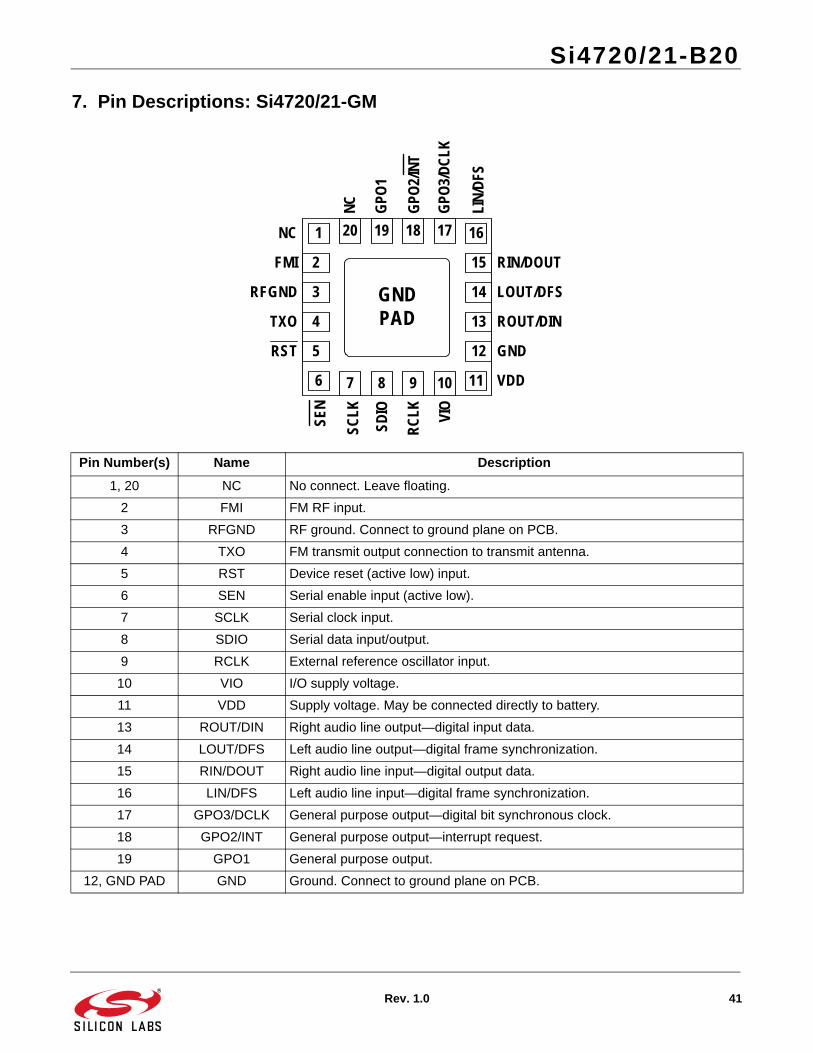
Si4720/21-B20
Rev. 1.0 41
7. Pin Descriptions: Si4720/21-GM
Pin Number(s) Name Description
1, 20 NC No connect. Leave floating.
2 FMI FM RF input.
3 RFGND RF ground. Connect to ground plane on PCB.
4 TXO FM transmit output connection to transmit antenna.
5 RST Device reset (active low) input.
6 SEN Serial enable input (active low).
7 SCLK Serial clock input.
8 SDIO Serial data input/output.
9 RCLK External reference oscillator input.
10 VIO I/O supply voltage.
11 VDD Supply voltage. May be connected directly to battery.
13 ROUT/DIN Right audio line output—digital input data.
14 LOUT/DFS Left audio line output—digital frame synchronization.
15 RIN/DOUT Right audio line input—digital output data.
16 LIN/DFS Left audio line input—digital frame synchronization.
17 GPO3/DCLK General purpose output—digital bit synchronous clock.
18 GPO2/INT General purpose output—interrupt request.
19 GPO1 General purpose output.
12, GND PAD GND Ground. Connect to ground plane on PCB.
GNDPAD
1
2
3
17181920
11
12
13
14
6 7 8 9
4
5
16
10
15
GPO
2/IN
T
VIO
RIN/DOUT
LOUT/DFS
ROUT/DIN
GNDRST
NC
TXO
RC
LK
SDIO
VDD
FMI
RFGND
GPO
3/D
CLK
NC
GPO
1
LIN
/DFS
SCLK
SEN

Si4720/21-B20
42 Rev. 1.0
8. Ordering Guide
Part Number* Description PackageType
OperatingTemperature
Si4720-B20-GM Broadcast FM Radio Transceiver for Portable Applica-tions
QFNPb-free
–20 to 85 °C
Si4721-B20-GM Broadcast FM Radio Transceiver for Portable Applica-tions with RDS/RBDS Encoder/Decoder
QFNPb-free
–20 to 85 °C
*Note: Add an “(R)” at the end of the device part number to denote tape and reel option; 2500 quantity per reel.

Si4720/21-B20
Rev. 1.0 43
9. Package Markings (Top Marks)
9.1. Top Mark Explanation
9.2. Si4720/21 Top Mark
9.3. Si4721 Top Mark
Mark Method: YAG Laser
Line 1 Marking: Part Number 20 = Si4720; 21 = Si4721
Firmware Revision 20 = Firmware Revision 2.0
Line 2 Marking: Die Revision B = Revision B Die
TTT = Internal Code Internal tracking code.
Line 3 Marking: Circle = 0.5 mm Diameter(Bottom-Left Justified)
Pin 1 Identifier
Y = YearWW = ‘Workweek
Assigned by the Assembly House. Corresponds to the last significant digit of the year and workweek of the mold date.
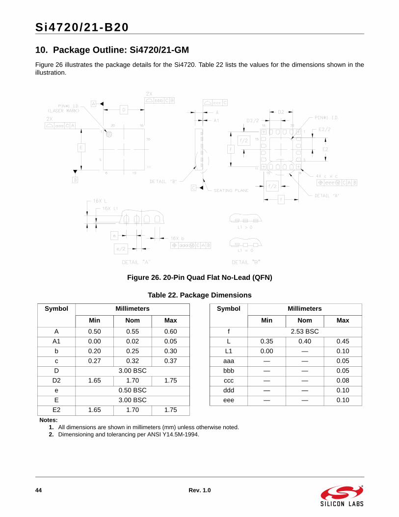
Si4720/21-B20
44 Rev. 1.0
10. Package Outline: Si4720/21-GM
Figure 26 illustrates the package details for the Si4720. Table 22 lists the values for the dimensions shown in theillustration.
Figure 26. 20-Pin Quad Flat No-Lead (QFN)
Table 22. Package Dimensions
Symbol Millimeters Symbol Millimeters
Min Nom Max Min Nom Max
A 0.50 0.55 0.60 f 2.53 BSC
A1 0.00 0.02 0.05 L 0.35 0.40 0.45
b 0.20 0.25 0.30 L1 0.00 — 0.10
c 0.27 0.32 0.37 aaa — — 0.05
D 3.00 BSC bbb — — 0.05
D2 1.65 1.70 1.75 ccc — — 0.08
e 0.50 BSC ddd — — 0.10
E 3.00 BSC eee — — 0.10
E2 1.65 1.70 1.75
Notes:1. All dimensions are shown in millimeters (mm) unless otherwise noted.2. Dimensioning and tolerancing per ANSI Y14.5M-1994.

Si4720/21-B20
Rev. 1.0 45
11. PCB Land Pattern: Si4720/21-GM
Figure 27 illustrates the PCB land pattern details for the Si4720-GM. Table 23 lists the values for the dimensionsshown in the illustration.
Figure 27. PCB Land Pattern

Si4720/21-B20
46 Rev. 1.0
Table 23. PCB Land Pattern Dimensions
Symbol Millimeters Symbol Millimeters
Min Max Min Max
D 2.71 REF GE 2.10 —
D2 1.60 1.80 W — 0.34
e 0.50 BSC X — 0.28
E 2.71 REF Y 0.61 REF
E2 1.60 1.80 ZE — 3.31
f 2.53 BSC ZD — 3.31
GD 2.10 —
Notes: General1. All dimensions shown are in millimeters (mm) unless otherwise noted.2. Dimensioning and tolerancing is per the ANSI Y14.5M-1994 specification.3. This land pattern design is based on IPC-SM-782 guidelines.4. All dimensions shown are at Maximum Material Condition (MMC). Least Material
Condition (LMC) is calculated based on a fabrication allowance of 0.05 mm.
Note: Solder Mask Design 1. All metal pads are to be non-solder-mask-defined (NSMD). Clearance between the
solder mask and the metal pad is to be 60 mm minimum, all the way around the pad.
Notes: Stencil Design1. A stainless steel, laser-cut and electro-polished stencil with trapezoidal walls should
be used to assure good solder paste release.2. The stencil thickness should be 0.125 mm (5 mils).3. The ratio of stencil aperture to land pad size should be 1:1 for the perimeter pads.4. A 1.45 x 1.45 mm square aperture should be used for the center pad. This provides
approximately 70% solder paste coverage on the pad, which is optimum to assure correct component standoff.
Notes: Card Assembly1. A No-Clean, Type-3 solder paste is recommended.2. The recommended card reflow profile is per the JEDEC/IPC J-STD-020C
specification for small body components.

Si4720/21-B20
Rev. 1.0 47
12. Additional Reference Resources
Si47xx Evaluation Board User’s Guide
AN307: Si4712/13/20/21 Receive Power Scan
AN332: Universal Programming Guide
AN341: Si4720/21 Evalution Board Quick Start Guide
AN383: Universal Antenna Selection and Layout Guidelines
AN388: Universal Evaluation Board Test Procedure
Si4720/21 Customer Support Site: www.mysilabs.comThis site contains all application notes, evaluation board schematics and layouts, and evaluation software. NDA is required for access. To request access, send mysilabs user name and request for access to [email protected].

Smart. Connected. Energy-Friendly.
Productswww.silabs.com/products
Qualitywww.silabs.com/quality
Support and Communitycommunity.silabs.com
http://www.silabs.com
Silicon Laboratories Inc.400 West Cesar ChavezAustin, TX 78701USA
DisclaimerSilicon Labs intends to provide customers with the latest, accurate, and in-depth documentation of all peripherals and modules available for system and software implementers using or intending to use the Silicon Labs products. Characterization data, available modules and peripherals, memory sizes and memory addresses refer to each specific device, and "Typical" parameters provided can and do vary in different applications. Application examples described herein are for illustrative purposes only. Silicon Labs reserves the right to make changes without further notice to the product information, specifications, and descriptions herein, and does not give warranties as to the accuracy or completeness of the included information. Without prior notification, Silicon Labs may update product firmware during the manufacturing process for security or reliability reasons. Such changes will not alter the specifications or the performance of the product. Silicon Labs shall have no liability for the consequences of use of the information supplied in this document. This document does not imply or expressly grant any license to design or fabricate any integrated circuits. The products are not designed or authorized to be used within any FDA Class III devices, applications for which FDA premarket approval is required or Life Support Systems without the specific written consent of Silicon Labs. A "Life Support System" is any product or system intended to support or sustain life and/or health, which, if it fails, can be reasonably expected to result in significant personal injury or death. Silicon Labs products are not designed or authorized for military applications. Silicon Labs products shall under no circumstances be used in weapons of mass destruction including (but not limited to) nuclear, biological or chemical weapons, or missiles capable of delivering such weapons. Silicon Labs disclaims all express and implied warranties and shall not be responsible or liable for any injuries or damages related to use of a Silicon Labs product in such unauthorized applications.
Trademark InformationSilicon Laboratories Inc.® , Silicon Laboratories®, Silicon Labs®, SiLabs® and the Silicon Labs logo®, Bluegiga®, Bluegiga Logo®, ClockBuilder®, CMEMS®, DSPLL®, EFM®, EFM32®, EFR, Ember®, Energy Micro, Energy Micro logo and combinations thereof, "the world’s most energy friendly microcontrollers", Ember®, EZLink®, EZRadio®, EZRadioPRO®, Gecko®, Gecko OS, Gecko OS Studio, ISOmodem®, Precision32®, ProSLIC®, Simplicity Studio®, SiPHY®, Telegesis, the Telegesis Logo®, USBXpress® , Zentri, the Zentri logo and Zentri DMS, Z-Wave®, and others are trademarks or registered trademarks of Silicon Labs. ARM, CORTEX, Cortex-M3 and THUMB are trademarks or registered trademarks of ARM Holdings. Keil is a registered trademark of ARM Limited. Wi-Fi is a registered trademark of the Wi-Fi Alliance. All other products or brand names mentioned herein are trademarks of their respective holders.