si-interposer design for gpu- memory integration...
TRANSCRIPT

DesignCon 2013
Si-interposer Design for GPU-Memory Integration concerning the Signal Integrity Jonghyun Cho, KAIST [[email protected]] Joohee Kim, KAIST [[email protected]] Hyun-Cheol Bae, ETRI [[email protected]] Kwangseong Choi, ETRI [[email protected]] Seungwook Paek, KAIST [[email protected]] Lee-Sup Kim, KAIST [[email protected]] Joungho Kim, KAIST [[email protected]]
Abstract Even 3-dimensional integrated circuit (3D-IC) has several advantages, it faces
difficulties in the mass production due to the low-fabrication yields. As an alternative solution for 3D-IC, many companies pay attention to a 2.5D-IC with interposer. In this paper, we investigate various design issues of 2.5D Si-interposer for GPU-Memory system, which consists of GPU, memory, and Si-interposer. The Si-interposer is designed using 2-layer re-distribution layer (RDL) and TSV. In the design, the lossy silicon substrate and the limited number of RDL layers cause several design issues such as routability, signal loss, crosstalk, and impedance mismatching. Because our target data frequency is only 50 MHz, these issues cause only a small effect on signal integrity of our system. However, high bandwidth is generally required in Si-interposer and a Si-interposer design for maximum bandwidth is proposed by considering these design issues at the same time. Eye-diagram is used for the evaluation of Si-interposer signal integrity. The Si-interposer is designed considering these signal integrity issues and it is in progress of fabrication. Author(s) Biography Jonghyun Cho received B.S. and M.S. degree in electrical engineering from Korea Advanced Institute of Science and Technology (KAIST), Daejeon, Korea, in 2008 and 2010, respectively. He is now a Ph.D. candidate in electrical engineering from KAIST. His research interests include Si-interposer design, TSV noise coupling, and TSV depletion effects in TSV-based 3D IC. Joohee Kim received B.S. and M.S. degree in electrical engineering from Korea Advanced Institute of Science and Technology (KAIST), Daejeon, Korea, in 2008 and 2010, respectively. She is currently pursuing the Ph.D. degree in electrical engineering from KAIST. Her research interests include TSV modeling and power consumption and failure analysis in TSV-based 3D IC. Hyun-Cheol Bae received the B.S. and M.S. degrees in electrical engineering from Dongguk University, Seoul, Korea, in 1999 and 2001, respectively, and the Ph.D. degree in electrical engineering from Chungnam National University, Daejeon, Korea, in 2009. He joined the SiGe Research Team, Electronics and Telecommunications Research Institute (ETRI) Daejeon, Korea, in 2001, as a Design and Process Engineer for MMIC and passive devices. He joined the Package Research Group, ETRI, in 2008, as a Packaging Engineer. His current research interests include 3-D stacked chip packaging using through-silicon-via and microelectromechanical systems wafer level packaging. Kwangseong Choi received the B.S. degree from Hanyang University, Seoul, Korea, and the M.S. and Ph.D. degrees from the Korea Advanced Institute of Science and Technology, Daejeon, Korea. He was engaged in development of chip scale packages, PoP packages, and designed high-speed electronic packages for DDR, Rambus, and RF devices with Hynix Semiconductor, Inc., Seoul, from 1995 to 2001. He has been involved in development of high-speed packaging technologies for optical devices such as modulators and receivers, since 2001, with the Electronics and Telecommunications
Research Institute (ETRI), Daejeon. He is the Team Leader of the Package Research Team, ETRI. His current research interests include the development of the materials and processes for 3-D integrated circuits with through-silicon-via. Seungwook Paek received the B.S. and M.S. degree in electrical engineering from Korea Advanced Institute of Science and Technology (KAIST), Daejeon, Korea, in 2009 and 2010 respectively, where he is currently pursuing the Ph.D. degree in electrical engineering. His research interests include computer-vision-inspired thermal analysis algorithm and its on-chip implementation. Lee-Sup Kim received the B.S. degree in electronics engineering from Seoul National University, Seoul, Korea, in 1982, and the M.S. and Ph.D. degrees in electrical engineering from Stanford University, Stanford, CA, in 1986 and 1990, respectively. He was a Post-Doctoral Research Fellow with Toshiba Corporation, Kawasaki, Japan, from 1990 to 1993, where he was involved with the design of the high-performance digital signal processor and single-chip MPEG2 decoder. Since March 1993, he has been with the Korea Advanced Institute of Science and Technology (KAIST), Daejeon, Korea, where he became a Professor in September 2002. He is currently with the MVLSI Laboratory, Department of Electrical Engineering, KAIST. In 1998, he was on sabbatical leave with Chromatic Research and SandCraft, Inc., Sunnyvale, CA. His current research interests include 3-D graphics processing unit design and high-speed/low-power mixed-mode integrated circuit design. Joungho Kim received B.S. and M.S. degrees in electrical engineering from Seoul National University, Seoul, Korea, in 1984 and 1986, respectively, and Ph.D degree in electrical engineering from the University of Michigan, Ann Arbor, in 1993. He is currently a Professor at Electrical Engineering and Computer Science Department. His major research topic is focused on chip-package co-design and simulation for signal integrity, power integrity, ground integrity, timing integrity, and radiated emission in 3D semiconductor packages, system-in-package(System-in-package), and SoP(System-on-package). Dr. Joungho Kim has been the chair or the co-chair of the EDAPS workshop since 2002. Currently, he is an Associated Editor of the IEEE Transactions of Electromagnetic Compatibility.
1. Introduction Recently, through-silicon via (TSV) based 3 dimensional integrated circuits (3D-ICs) are emerging as a key solution of the future electronics. By Moore’s law, the transistor density doubles every 18 months and the transistor size scaling leads to satisfy the law until now. However, it encounters several limitations such as lithography difficulty, high static power consumption of transistor, and increased manufacturing process cost [1]. In TSV based 3D-ICs, chips are stacked vertically and TSVs are used for the vertical interconnection between stacked dies. Because a TSV has much shorter length than conventional wire-bonding and can be located at any place of a stacked die, both I/O number and maximum transfer frequency could increase. It greatly increases the system bandwidth and the transistor density per planar area also greatly increases. Although there are several advantages of 3D-ICs, some disadvantages also exist. Heat cannot be released from hot spots to the air because stacked chips prevent heat transfer through the z-direction. TSV noise can be easily coupled to the adjacent TSV through conductive silicon substrate [2-3]. Above all things, manufacturing issues are the main problem of TSV based 3D-IC. For the TSV based 3D-IC system, several manufacturing steps are necessary. In the assumption of via-middle TSV process, MOS devices are manufactured, and then TSV are formed. After TSV manufacturing, MOS devices and TSVs are connected using metal lines and then, stacking process starts. Finally, stacked chips are packaged and final products are made. These are much more complicated steps and the total yields decreases a lot compared with 2D-IC. Thousands of TSVs should be successfully made and correctly bonded. Also the MOS devices should be well manufactured at the same time. Because TSV technology is not mature now, TSV manufacturing and bonding yields are not good. Additionally, there’s no efficient way to detect TSV and MOS device failures and replace them with redundant TSV and circuits [4]. This yield problem becomes more and more severe as 3D-IC system becomes more complicated. Because of these difficulties at the 3D-IC manufacturing process, 2.5D-IC emerges as a temporary solution until 3D-IC manufacturing process becomes mature [5]. In 2.5D-IC, several chips are stacked on interposer and only homogeneous chip stacking is used. A processor and stacked memory on interposer is a representative example of 2.5D-IC configuration as illustrated in Fig. 1. To increase bandwidth between laterally placed processor and memories, fine-pitch metal routing is necessary because it increase I/O counts. For this purpose, an interposer is used where small width and small space metal routing is possible. And silicon substrate is usually used for an interposer because on-silicon metallization process is mature and fine-pitch metal routing is possible. Furthermore, the loss of silicon substrate greatly affects signal transmission on silicon interposer. As a result, several signal integrity (SI) issues occur such as signal loss, signal line characteristic impedance and crosstalk between signal traces. In this paper, silicon interposer design procedure is explained for GPU and memory integration. Both GPU and memory are manufactured by Samsung 0.13 process and the silicon interposer metal lines and TSVs are manufactured by EPWORKs. Because we used SRAM as a memory, the communication between GPU and memory is done with very low speed and the SI and PI issues are not severe in this case. However, we propose a general design procedure assuming high-speed digital communication between GPU and memory. The simulation-based design procedure and design guides of silicon

interposer for high bandwidth system are first presented, and then the designed silicon interposer for GPU and memory integration is analyzed in SI respects.
Figure 1. The representative example of 2.5D-IC configuration: stacked memory and processor are stacked
on silicon interposer. The silicon interposer and PKG are connected using TSVs. 2. Considerations for Silicon Interposer Design In this paper, GPU and memory are integrated on silicon interposer and the silicon interposer design issues are analyzed in the respect of SI and PI. To start silicon interposer design for the GPU and memory integration, several things should be determined. First, the silicon interposer manufacturing process should be determined such as metal stack-up, metal design rules, TSV size, and TSV design rules. In our case, EPWORKs is in charge of the silicon interposer manufacturing and ETRI integrates GPU and memory on the silicon interposer by using flip-chip bonding and the interposer is bonded on PCB. We used only two metal layers: M1 has 0.5 um distance from the silicon substrate while M2 has 8 um far from the silicon. The thickness for M1 and M2 metal is 3 um. The minimum width and space of metal is 10 um. For TSV, the diameter is 40 um and the insulation layer thickness is 1 um. GPU and memory net lists are also necessary for the design. We should know which I/Os are connected each other and which I/Os are connected to the outer pins. GPU and memory transceiver spec and the data frequency is very critical factor to the design considering SI and PI. For the GPU, digital circuit design is performed using Samsung 0.13 process. For the memory, we decided to use SRAM and it is also designed using Samsung 0.13 process. Although the chip design is not our main purpose, GPU and SRAM are designed because of the difficulties to get the GPU and memory bare-dies compatible with the following-up processes. Also, we used a large number of phantom cells, which Samsung provides and stable operations are guaranteed. By using phantoms cells, more easy and stable design is possible, but we cannot access to the internal circuit of the phantoms cells due to the security and only digital simulations are possible. In our case, the data speed between GPU and SRAM is less than 50 MHz due to the SRAM’s low speed and only the digital simulation is acceptable. SI and PI issues almost not occur at this frequency. Even though, the SI and PI issues are negligible for this case, our goal is not fixed to this specific case, but the general cases. We will consider general silicon interposer design for GPU and memory integration for this process and the real silicon interposer design would be analyzed. Generally, we want to maximize the bandwidth between GPU and memory by using 2.5D configuration. In the respect of SI, signal loss, crosstalk, and characteristic impedance

mismatching are the main limitations for the system bandwidth. Because we use silicon as substrate, the loss is much severe than the conventional organic PCB/PKG. Dense signal routing generates large crosstalk and also the characteristic impedance mismatching affects bandwidth. These effects are analyzed for silicon interposer case and eye-diagram is proposed to evaluate the silicon interposer design.
Figure 2. Total system configurations including GPU and SRAM stacked silicon interposer
3. Signal Integrity Analysis in 2.5D Silicon Interposer 3-1. Silicon Line Loss and characteristic Impedance In our target silicon interposer, we use only two metal layers for the signal routing and coplanar-type transmission line is only a practical solution. We assume GSG coplanar-type transmission line on silicon substrate. Because of high loss of silicon, metal routing using M1 layer experiences much higher loss compared with the M2 metal routing. For M1 and M2 routing, EM-simulation is performed using Ansys HFSS and the results are illustrated in Fig. 3. For the insertion loss, 50 Ω is used for the terminations and the metal width and space is chosen to be the minimum allowable value, 10 um, and the line length is 5 mm. Also, eye-diagram is plotted at 1.4Gbps using the simulated s-parameter and is illustrated in Fig. 4. For the transceiver termination, we assumed that transmitter resistance is 80 ohm and receiver capacitance is 1.5 pF [6] because we don’t know the internal circuit of GPU and memory transceiver due to the use of phantom cell.

Figure 3. Insertion loss of GSG coplanar-type transmission lines on silicon interposer using M1 and M2
layer. The simulated line width is 10 um, space is 10 um, and length is 5 mm
(a) (b)
Figure 4. Eye-diagram of on-interposer GSG coplanar-type transmission line: (a) 5 mm routing at M1 layer and (b) 5 mm routing at M2 layer
As frequency increases, the insertion loss difference between M1 and M2 becomes great and M2 routing is much preferable than M1 routing. If we use M1 layer for the signal routing, eye-height decreases, jitter increases, and the maximum data speed decreases. It could be explained as the characteristics of on-silicon metal lines. The simplified lumped circuit model of on-silicon metal line and its equivalent C, G model are illustrated in Fig. 5. The insulation layer capacitance, Cinsulator, exists between metal and silicon, and the silicon C and G is serially added to the Cinsulator. The equations for the equivalent C and G are listed below.
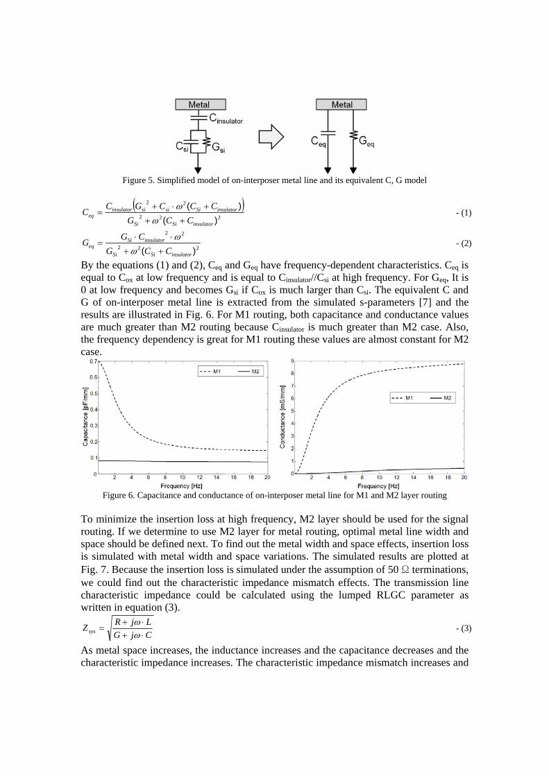
Figure 5. Simplified model of on-interposer metal line and its equivalent C, G model
( )
222
22
)()(
insulatorSiSi
insulatorSisisiinsulatoreq CCG
CCCGCC
++
+⋅+=
ωω - (1)
222
22
)( insulatorSiSi
insulatorSieq CCG
CGG
++
⋅⋅=
ωω - (2)
By the equations (1) and (2), Ceq and Geq have frequency-dependent characteristics. Ceq is equal to Cox at low frequency and is equal to Cinsulator//Csi at high frequency. For Geq, It is 0 at low frequency and becomes Gsi if Cox is much larger than Csi. The equivalent C and G of on-interposer metal line is extracted from the simulated s-parameters [7] and the results are illustrated in Fig. 6. For M1 routing, both capacitance and conductance values are much greater than M2 routing because Cinsulator is much greater than M2 case. Also, the frequency dependency is great for M1 routing these values are almost constant for M2 case.
Figure 6. Capacitance and conductance of on-interposer metal line for M1 and M2 layer routing
To minimize the insertion loss at high frequency, M2 layer should be used for the signal routing. If we determine to use M2 layer for metal routing, optimal metal line width and space should be defined next. To find out the metal width and space effects, insertion loss is simulated with metal width and space variations. The simulated results are plotted at Fig. 7. Because the insertion loss is simulated under the assumption of 50 Ω terminations, we could find out the characteristic impedance mismatch effects. The transmission line characteristic impedance could be calculated using the lumped RLGC parameter as written in equation (3).
CjGLjRZsys ⋅+⋅+
=ωω - (3)
As metal space increases, the inductance increases and the capacitance decreases and the characteristic impedance increases. The characteristic impedance mismatch increases and

the insertion loss graph have a sharp bend depending on frequency. The overall loss increases because the inductance increases. On the other hands, characteristic impedance mismatch effects decrease as metal width increases. The insertion loss graph has more straight line depending on frequency.
Figure 7. The insertion loss of on-interposer transmission lines using M2 layer. 5 simulation results are
plotted with metal width and space of variation between 10 um and 20 um The characteristic impedance graphs for several metal width and spaces are plotted in Fig. 8. Because C increases as metal width increases and L increases as metal space increases, the characteristic impedance increases as metal space increases while it decreases as metal width increases as we expected using the equation (3). For M1 metal line, it changes depending on frequency up to about 10 GHz because equivalent C and G changes depending on frequency up to that frequency.
Figure 8. The characteristic impedance of on-interposer metal line. Imaginary terms have small value and
ignored in this plot. It changes depending on frequency.
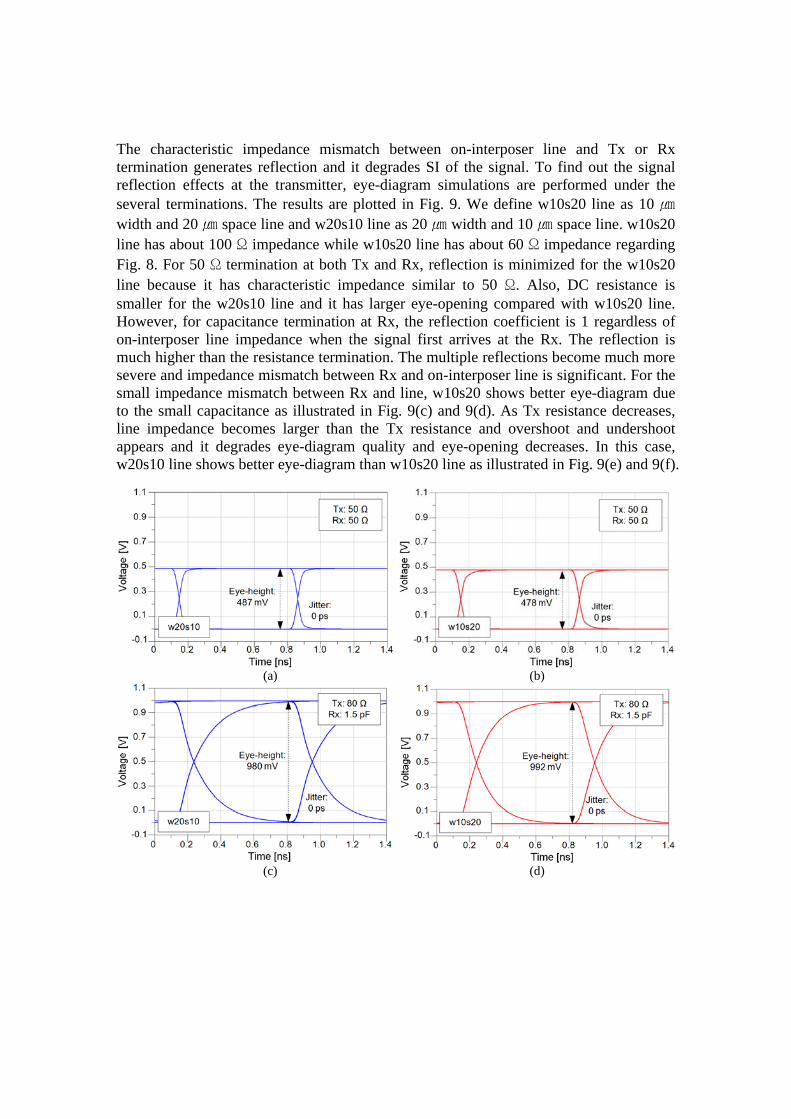
The characteristic impedance mismatch between on-interposer line and Tx or Rx termination generates reflection and it degrades SI of the signal. To find out the signal reflection effects at the transmitter, eye-diagram simulations are performed under the several terminations. The results are plotted in Fig. 9. We define w10s20 line as 10 width and 20 space line and w20s10 line as 20 width and 10 space line. w10s20 line has about 100 Ω impedance while w10s20 line has about 60 Ω impedance regarding Fig. 8. For 50 Ω termination at both Tx and Rx, reflection is minimized for the w10s20 line because it has characteristic impedance similar to 50 Ω. Also, DC resistance is smaller for the w20s10 line and it has larger eye-opening compared with w10s20 line. However, for capacitance termination at Rx, the reflection coefficient is 1 regardless of on-interposer line impedance when the signal first arrives at the Rx. The reflection is much higher than the resistance termination. The multiple reflections become much more severe and impedance mismatch between Rx and on-interposer line is significant. For the small impedance mismatch between Rx and line, w10s20 shows better eye-diagram due to the small capacitance as illustrated in Fig. 9(c) and 9(d). As Tx resistance decreases, line impedance becomes larger than the Tx resistance and overshoot and undershoot appears and it degrades eye-diagram quality and eye-opening decreases. In this case, w20s10 line shows better eye-diagram than w10s20 line as illustrated in Fig. 9(e) and 9(f).
(a) (b)
(c) (d)

(e) (f)
Figure 9. Eye-diagram with variations in metal width, space, and terminations: (a) 20 width, 10 space, Tx 50 Ω, and Rx 50 Ω (b) 10 width, 20 space, Tx 50 Ω, and Rx 50 Ω (c) 20 width, 10 space,
Tx 80 Ω, and Rx 1.5 pF (d) 10 width, 20 space, Tx 80 ohm, and Rx 1.5 pF (e) 20 width, 10
space, Tx 40 Ω, and Rx 1.5 pF (f) 10 width, 20 space, Tx 40 Ω, and Rx 1.5 pF 3-2. Stub Effects For the target interposer, GPU and memory communicate each other and some of this signal is also connected to the outer interface because GPU shares this trace as the control pin. For this purpose, on-interposer line for GPU and memory connection has a stub and it greatly affects the SI quality of the receive signal. For the M2 GSG-type coplanar line with 5000 um length, the eye-diagram at receiver is illustrated in Fig. 10 with and without a stub. The input signal is 1 V, 1.4Gbps PRBS with 50 ps rising and falling time and the input resistance is 80 ohm and the output termination is 1.5 pF.
(a) (b) (c)
Figure 10. Eye-diagram at receiver with 1V 50ps rising time PRBS is inserted at transmitter. The Tx termination is 80 Ω and The Rx and stub termination is 1.5 pF: (a) Eye-diagram with no stub, (b) Eye-
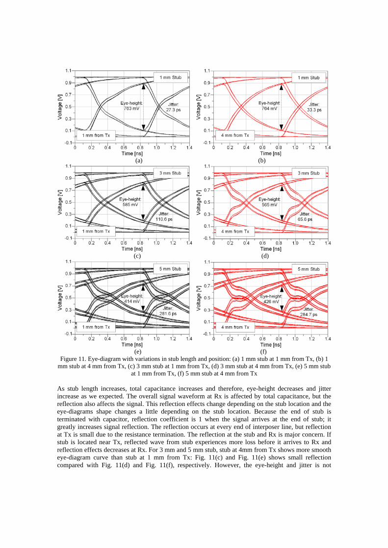
diagram with 3 mm M1 stub, and (c) Eye-diagram with 3 mm M2 stub If there’s no stub, the eye-diagram shows good quality as plotted in Fig. 10(a). However, if there exist a stub, line capacitance and termination capacitance at the end of stub is added to the original capacitance. It greatly increases total capacitance and the eye-diagram quality becomes worse. If the sub is generated using the M2 layer, stub line capacitance decreases and eye-height increases and jitter decreases. If a stub is necessarily used for several reasons, M2 line is much preferable for the stub to increase SI quality. However, it is very limited due to the routability issues. M2 line is used for the GPU and memory interconnection and there’s no space for the stub routing and stub should be routed using M1 layer in this case. For the stub design, the location of stub is also important. For the fixed length of M2 line of 5 mm, M1 stub is added in the different position and the receiver eye-diagram is plotted in Fig. 11. Also, the eye-diagram with different length of M1 stub is plotted in that figure.
(a) (b)
(c) (d)
(e) (f)
Figure 11. Eye-diagram with variations in stub length and position: (a) 1 mm stub at 1 mm from Tx, (b) 1 mm stub at 4 mm from Tx, (c) 3 mm stub at 1 mm from Tx, (d) 3 mm stub at 4 mm from Tx, (e) 5 mm stub
at 1 mm from Tx, (f) 5 mm stub at 4 mm from Tx As stub length increases, total capacitance increases and therefore, eye-height decreases and jitter increase as we expected. The overall signal waveform at Rx is affected by total capacitance, but the reflection also affects the signal. This reflection effects change depending on the stub location and the eye-diagrams shape changes a little depending on the stub location. Because the end of stub is terminated with capacitor, reflection coefficient is 1 when the signal arrives at the end of stub; it greatly increases signal reflection. The reflection occurs at every end of interposer line, but reflection at Tx is small due to the resistance termination. The reflection at the stub and Rx is major concern. If stub is located near Tx, reflected wave from stub experiences more loss before it arrives to Rx and reflection effects decreases at Rx. For 3 mm and 5 mm stub, stub at 4mm from Tx shows more smooth eye-diagram curve than stub at 1 mm from Tx: Fig. 11(c) and Fig. 11(e) shows small reflection compared with Fig. 11(d) and Fig. 11(f), respectively. However, the eye-height and jitter is not
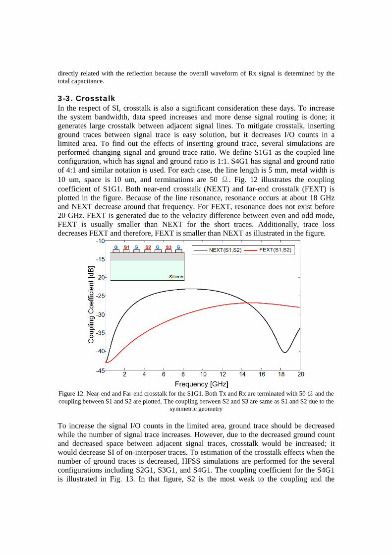
directly related with the reflection because the overall waveform of Rx signal is determined by the total capacitance. 3-3. Crosstalk In the respect of SI, crosstalk is also a significant consideration these days. To increase the system bandwidth, data speed increases and more dense signal routing is done; it generates large crosstalk between adjacent signal lines. To mitigate crosstalk, inserting ground traces between signal trace is easy solution, but it decreases I/O counts in a limited area. To find out the effects of inserting ground trace, several simulations are performed changing signal and ground trace ratio. We define S1G1 as the coupled line configuration, which has signal and ground ratio is 1:1. S4G1 has signal and ground ratio of 4:1 and similar notation is used. For each case, the line length is 5 mm, metal width is 10 um, space is 10 um, and terminations are 50 Ω. Fig. 12 illustrates the coupling coefficient of S1G1. Both near-end crosstalk (NEXT) and far-end crosstalk (FEXT) is plotted in the figure. Because of the line resonance, resonance occurs at about 18 GHz and NEXT decrease around that frequency. For FEXT, resonance does not exist before 20 GHz. FEXT is generated due to the velocity difference between even and odd mode, FEXT is usually smaller than NEXT for the short traces. Additionally, trace loss decreases FEXT and therefore, FEXT is smaller than NEXT as illustrated in the figure.
Figure 12. Near-end and Far-end crosstalk for the S1G1. Both Tx and Rx are terminated with 50 Ω and the coupling between S1 and S2 are plotted. The coupling between S2 and S3 are same as S1 and S2 due to the
symmetric geometry To increase the signal I/O counts in the limited area, ground trace should be decreased while the number of signal trace increases. However, due to the decreased ground count and decreased space between adjacent signal traces, crosstalk would be increased; it would decrease SI of on-interposer traces. To estimation of the crosstalk effects when the number of ground traces is decreased, HFSS simulations are performed for the several configurations including S2G1, S3G1, and S4G1. The coupling coefficient for the S4G1 is illustrated in Fig. 13. In that figure, S2 is the most weak to the coupling and the

coupling coefficient between S2 and other signal traces are plotted in the figure. S1 and S3 are closely located to S2, but S1 has ground trace at the very next to the S1 and coupling between S2 and S3 is the most severe. Also, increased capacitance and inductance makes the resonance frequency shift to the lower frequency.
Figure 13. Near-end and Far-end crosstalk for the S1G1. Both Tx and Rx are terminated with 50 Ω and the coupling between S2 and adjacent traces are plotted. The coupling between S2 and S3 are the most severe.
The coupling coefficient in Fig. 13 and Fig. 14 are plotted in the assumption of 50 Ω terminations both at Tx and Rx and it is not a practical situation. The terminations are changed to Tx of 80 Ω and Rx of 1.5 pF and time-domain simulation is performed. Even though there are three or four signal traces, all signal traces are assumed to be quiet except on aggressor signal. 1V, 1.4Gbps clock signal with rising and falling time of 50 ps is selected as the aggressor signal and the coupling noise is simulated at the adjacent victim traces. For S1G1, S1 is aggressor and S2 is the victim and the results are illustrated in Fig. 14. For the capacitance termination at Rx, peak-to-peak noise voltage is larger for NEXT than FEXT. We are interested in the SI at Rx and FEXT is much more our concern than NEXT and is only 15.3 mV in this case. For general digital or analog system, this level of coupling is acceptable and the SI would be guaranteed.
(a) (b)

Figure 14. The coupling noise at near and far-end for S1G1 configuration. The terminations of Tx is 80 Ω and Rx is terminated with 1.5 pF. Input is 1.4Gbps clock signal with rising and falling time of 50ps.
S4G1 is also simulated at the same environment. The victim is S3 and the aggressor is chosen to be S2, which generates the maximum noise to the victim. The results are plotted in Fig. 15. Because the aggressor and the victim trace are closely located and the ground traces are located far from the signal traces, the peak to peak coupling noise is much larger than the S1G1 case. Additionally, S1 and S4 also generate coupling noise at the victim signal and the total peak-to-peak coupling noise would be larger than 200 mV at the worst case. These large coupling degrades SI and could violate the design spec in some cases. Signal I/O counts per area are greatly increases compared with S1G1, SI quality becomes much worse.
(a) (b)
Figure 15. The coupling noise at near and far-end for S4G1 configuration. The terminations of Tx is 80 Ω and Rx is terminated with 1.5 pF. Input is 1.4Gbps clock signal with rising and falling time of 50ps.
3-4. Eye-diagram as a SI evaluation parameter Signal loss, reflection due to impedance mismatching, and crosstalk are the significant concern for SI considerable design. In practical situation, these issues occur at the same time and they should be considered at the same time for the accurate SI performance evaluation. An Eye-diagram is the best way to represent the signal quality considering these SI issues at the same time. For the eye-diagram of coupled traces, there’s a lot of combinations to construct the eye-diagram because each signal input is dependent to the other traces. The signal frequency, voltage, rising and falling time, and delay could be different at each signal traces. In practical situation for GPU and memory interconnection, the data frequency, voltage, rising and falling time is same. Additionally, the delay between each signal trace inputs could be assumed to be zero because data traces are usually synchronized to the clock. In this situation, the estimation of worst-case eye-diagram becomes much more simplified. The single-channel worst-case eye-diagram is calculated using the combination of worst case input ‘1’ and ‘0’. The worst-case ‘1’ is the sudden ‘1’ after long sequence of ‘0’ and after the input ‘1’, ‘0’ repeats again. The worst-case ‘0’ is similar to worst-case ‘0’ except that ‘0’ and ‘1’ are replaced by ‘1’ and ‘0’, respectively. For the coupled signals, the worst case ‘1’ and ‘0’ are the sudden ‘1’ and ‘0’ of victim trace when the other signal traces are same or opposite to the victim signal (Even and odd mode between signal traces) . Rigorously, this even- and odd- mode signaling do not guarantee the real worst case ‘1’ and ‘0’. However, it could be used as

worst case ‘1’ and ‘0’ in general cases because the rising and falling time of the signal at Rx is usually determined by the resistance and the capacitance of the signal trace [8]. The eye-diagram is simulated by the combination of even- and odd- mode signaling and the results are illustrated in Fig. 16. As signal to ground ratio increases, eye-height decreases a little while jitter increases a lot. Because signal switches at the same time, several hundreds mV of noise does not appear at the victim signal. Instead, signal delay, rising and falling time changes depending on the adjacent victim signal trace status depending on the mode condition. At even mode, victim signal does not experience mutual capacitance while it experiences double capacitance at odd mode. As a result, the even mode delay, rising and falling time is short while the odd mode delay, rising and falling time is long: It induces jitter to the victim signal. In this worst-case eye-diagram, signal trace loss, reflection, and crosstalk effects are included and could be used to evaluate the SI quality of designed Si-interposer.
(a) (b)
(c) (d)
Figure 16. Worst-case eye-diagram simulation results when signal and ground count ratio varies from 1:1 to 4:1. Signal inputs are assumed to be synchronized and 1V, 1.4Gbps PRBS with 50 ps rising and falling
time is used as the signal source.
Additionally, the eye-diagram simulation is performed for the interposer line with a stub and is plotted in Fig. 17. The line length and dimension is the same as that of Fig. 16, but 3 mm stub is connected. The simulation is performed as signal and ground count ratio changes. Because of the increased capacitance, eye-diagram quality is much degraded compared with the no stub case. As the signal to ground count ratio increase, eye-height decreases and jitter increase like the results of Fig. 16.

(a) (b)
(c) (d)
Figure 17. Worst-case eye-diagram simulation results with 3 mm M1 stub. The signal and ground count ratio varies from 1:1 to 4:1.
4. Case Study concerning SI Issues From now on, we studied the SI issues on silicon interposer based on the EPWORKS manufacturing specs: minimum metal width and space of 10 um and 2-metal layer routing. However, these SI issues occur at general Si-interposer design and general design guides would be proposed in this chapter. For the Si-interposer manufacturing, on-chip metal process could be used and metal routing would be done using fine-pitch routing is possible. In that case, metal width and space could be decreased down to 1 or below. At that case, signal trace resistance is expected to be important factor to the signal transmission. Also, the crosstalk level would be changed. To analyze these effects, worst-case eye-diagram simulation is performed for the decreased metal width and space. The results are plotted in Fig. 18. At the simulation, signal and ground count ratio is 4:1 and the crosstalk effects are included in the eye-diagram. For metal width and space of 1 , signal trace resistance is large and the eye-height is less than 900 mV. The eye-height increases as metal width and space increases, but if metal width and space is equal or larger than 4 , it has no effects. Concerning the jitter, metal width and space has a slight effect and it is minimized when metal width and space is 2 . For 1.4Gbps signaling, metal width and space has only a little effect and smaller metal width and space is desirable to reduce the routing area. The signal and ground count ratio affects crosstalk-induced jitter, but it could be neglected because simulated jitter is less than 60 ps for S4G1.

(a) (b)
(c) (d)
Figure 18. Worst-case eye-diagram simulation results when signal and ground count ratio is 4:1. The simulation is performed as the metal width and space is changes.
However, for the high data rate, metal width and space greatly affects SI quality at Rx. For 4.2Gbps, worst-case eye-diagram simulation is performed and the results are plotted in Fig. 19. To make a decision that this channel is acceptable or not, eye-height and jitter spec is necessary. The minimum eye-height and maximum jitter is defined as 500mV and 53.3 ps refer to the Skhynix GDDR3 data sheet [9]. In Fig. 19(a) and Fig. 19(b), eye-height and jitter violate this spec and this channel could not be used for the 4.2Gbps signal routing. If we increase the metal width and space, eye-height increases and jitter decrease under 4 . If the metal width and space is equal or larger than 4 , it has no effects like the case in Fig. 18. Because crosstalk effect is increased due to the increased signal frequency, crosstalk reduction design of interposer metal trace is necessary. For the S4G1 configuration, the jitter always violates the jitter spec and other configuration should be used to satisfy the spec. If we use S1G1 configuration, it satisfies the spec when metal width, space is equal to or larger than 4 .

(a) (b)
(c) (d)
Figure 19. Worst-case eye-diagram simulation results when signal to ground count ratio and metal width, space changes together. The input signal is 4.2Gbps PRBS with 50ps rising and falling time
5. Conclusion In this paper, SI issues for Si-interposer design are analyzed. Because of manufacturing difficulties and high cost of 3D-IC, 2.5D-IC using interposer becomes popular as an alternative solution. In Si-interposer, minimum metal width and space is smaller than conventional package and it could achieve the high-bandwidth between the laterally stacked chips. However, silicon substrate loss, characteristic impedance mismatch, and crosstalk between adjacent lines prevent data speed increase. These issues are separately analyzed and the eye-diagram is used to consider these SI issues at the same time. For M2 routing (8 apart from silicon and 3 thickness), the metal width, space, and signal and ground count ratio has small effects to SI at 1.4Gbps. 1 metal width and space with signal and ground count ratio of 4:1 could be used for small routing area. To achieve more high data rate, metal width, space, and ground counts should be increased. It decreases crosstalk and RC-delay. For 4.2Gbps signaling, signal and ground count of 4:1 is impossible due to the crosstalk. Also, metal width and space should increase to 4 or the higher. For high data rate signaling, more area is necessary and trade-offs exist. 6. Acknowledgement This article was supported by the IT R&D program of MKE/KEIT. [KI001472, Wafer Level 3D IC Design and Integration]

7. Reference [1] James D. Meindl, Qiang Chen, and Jeffrey A. Davis, “Limits on Silicon
Nanoelectronics for Terascale Integration,” Science, vol.293, no.5537, pp.2044-2049, 2001
[2] Kiran Puttaswamy and Gabriel H.Loh, “Thermal Analysis of a 3D Die-Stacked High-Performance Microprocessor,” Proceedings of the 16th ACM Great Lakes symposium on VLSI. ACM, 2006.
[3] Jonghyun Cho, Eakhwan Song, Kihyun Yoon, Jun So Pak, Joohee Kim, Woojin Lee, Taigon Song, Kiyeong Kim, Junho Lee, Hyungdong Lee, Kunwoo Park, Seungtaek Yang, Minsuk Suh, Kwangyoo Byun, and Joungho Kim, "Modeling and Analysis of Through-Silicon Via (TSV) Noise Coupling and Suppression Using a Guard Ring," IEEE Transactions on Components, Packaging and Manufacturing Technology (CPMT), vol.1, no.2, pp.220-233, Feb. 2011
[4] Ang-Chih Hsieh and TingTing Hwang, "TSV Redundancy: Architecture and Design Issues in 3-D IC," IEEE Transactions on Very Large Scale Integration (VLSI) Systems, vol.20, no.4, pp.711-722, April 2012
[5] Meng-Jen Wang, Chang-Ying Hung, Chin-Li Kao, Pao-Nan Lee, Chi-Han Chen, Chih-Pin Hung, and Ho-Ming Tong, "TSV technology for 2.5D IC solution," Electronic Components and Technology Conference (ECTC), 2012, pp.284-288, May 29 2012-June 1 2012
[6] Heegon Kim; Jonghyun Cho; Joohee Kim; Myunghoi Kim; Junho Lee; Hyungdong Lee; Kunwoo Park; Joungho Kim; Jun So Pak; , "Channel design for wide system bandwidth in a TSV based 3D IC," Signal Propagation on Interconnects (SPI), 2011, pp.57-60, 8-11 May 2011
[7] Joong-Ho Kim, Dan Oh, and Woopoung Kim, "Accurate Characterization of Broadband Multiconductor Transmission Lines for High-Speed Digital Systems," IEEE Transactions on Advanced Packaging, vol.33, no.4, pp.857-867, Nov. 2010
[8] Zhaoqing Chen and George Katopis, "Searching for the worst-case eye diagram of a signal channel in electronic packaging system including the effects of the nonlinear I/O devices and the crosstalk from adjacent channels," Electronic Components and Technology Conference (ECTC), 2009, pp.1106-1113, 26-29 May 2009
[9] SKhynix 512Mbit GDDR3 H5RS5223CRF datasheet