show daily - solid state technology | insights for...
TRANSCRIPT

A new name for the company that will result
in the pending merger between Applied Ma-
terials and Tokyo Electron Limited (TEL) was
announced on Monday evening at SEMICON
West prior to a gala event at The Palace hotel.
The new name will be Eteris (pronounced “eh-
TAIR-iss”), which the company said is derived
from the concept of “Eternal Innovation for
Society.” The name will go into effect once the
merger is complete.
At a press event, Tetsuro “Terry” Higashi,
Chairman, President and CEO of TEL and
Gary Dickerson, President and CEO of Ap-
plied Materials, took turns describing their
combined vision for the new company. They
said they have spent more than 50 days over
the last 10 months in face-to-face meetings.
Eteris Selected as New Name for Applied Materials, TEL Merged Company
JULY 9, 2014
MOSCONE CENTER | SAN FRANCISCO, CALIFORNIA
WEDNESDAYSHOW DAILYSHOW DAILYSHOW DAILY8:15am-9:00am GLOBAL SUMMIT FOR ADVANCED MANUFACTURING: Challenges and Opportunities in Semiconductor Technology for Manufacturing in ChinaShiuhWuu Lee, SMICSan Francisco Marriott Marquis, Golden Gate A
10:00am-10:45am KEYNOTE: The Art of the Possible: How Manufacturers are Leveraging Digital Technologies to Drive Business Transformation in a Connected WorldMr. Sanjay Ravi, Microsoft CorporationKeynote Stage, Moscone North, Room 135
10:30am-12:30pmSubcomponent Supply Chain Challenges for 10 nm and BeyondTechXPOT South, South Hall
10:30am-12:30pm Bringing Silicon Photonics to MarketTechXPOT North, North Hall
1:35pm-1:50pm ITRS LIthography Working Group UpdatePART OF THE STS SESSIONMoscone North, Hall E, Room 131
1:30pm-7:00pm Test Vision 2020 Workshop and ReceptionMoscone North, Hall E, Room 130
continued on p 3
Gary Dickerson, President and CEO of Applied Materials and Tetsuro Higashi, Chairman, President and CEO of TEL, revealed the new company name and logo on Monday.
DON’T MISS
A collection of the first fully patterned 450mm
wafers are on display at SEMICON West this
week at the newly merged SUNY CNSE/SUN-
YIT exhibit, booth 517, located in the Moscone
Center’s South Hall. The wafers will be on dis-
play throughout the exhibition and showcased
in the 450 mm Technology Development Ses-
sion on Thursday July 10th.
Fully patterned 450mm wafers have been
shown before, most notably those produced
using Molecular Imprints’ Imprio nanoimprint
lithography (NIL) tool. At SEMI’s ISS meeting
in Jaunary 2013, Intel’s Bob Bruck famously
held such a wafer before the crowd.
But the 450mm wafers on display this week
were produced using Nikon’s 193 immersion
scanner, making it the first of its kind using
conventional lithography tools now in use for
300mm wafer production.
“These first 450mm wafers are tangible
proof that the industry’s transition to this
next generation technology is on track and
gaining momentum,” said Paul Farrar, Jr.,
Vice President for Manufacturing Innovation
of the newly merged SUNY CNSE/SUNYIT
institution and General Manager of the G450C.
The Nikon immersion scanner will join
existing 450mm infrastructure at the Albany
NanoTech Complex in April of 2015 in accor-
dance with the project timeline. This critical
milestone will enable G450C founding mem-
bers and CNSE to perform 10nm and below,
full wafer photolithography, while optimizing
tool configuration and performance.
In July of 2013, New York’s Governor Cuomo
announced a $350 million partnership between
the newly merged CNSE/SUNYIT and Nikon
to develop next generation 450mm photolithog-
raphy technology. Nikon and the newly merged
First 450mm Wafers Patterned with Immersion Lithography
One of the first fully patterned 450mm wafers produced using conventional 193
immersion lithography.
continued on p 3

Visit Us At Booth #310, South Hall
www.highvac.com
Leader in Quality Vacuum Valves
For Your Most Demanding Applications Harsh Process Valves• Wedge design
• Isolated bellows
• Easy in-situ maintenance for reduced down time
• Resilient to aggressive chemicals & high temperatures
• Tough enough for harsh processes like MOCVD, ALD, & PECVD
Valves Designed for Semiconductor Processes & Sub-Fab Environment
When Safety And Security Are Your PriorityLockout/Tagout “LOTO” Valves • Failsafe (locked) closure for safe maintenance
• OSHA compliant under USDOL federal regulations
Slit ValvesAluminum Stainless

SHOW DAILY
WEDNESDAY | JULY 9, 2014
3SHOW DAILY
Shareholders of both companies have ap-
proved the transaction, but it is still under
antitrust review by multiple jurisdictions,
including the U.S. and China. Bob Halliday,
CFO of Applied Materials, said that they ex-
pect to get regulatory approval in time to close
the transaction in the second half of 2014.
Gary Dickerson described how both
companies were instrumental in improving
society. “Moore’s Law is one of the greatest
technology innovations that have changed
the world and improved the way people live,”
he said. “Both companies, Tokyo Electron
and Applied Materials, have really been fun-
damental to this incredible technology that
we’ve been able to produce within the semi-
conductor industry. Our goal is to take those
core technologies, competencies and incred-
ible talent and expand into new markets.”
Dickerson said the new company will be
focused on precision materials engineer-
ing and accelerating materials innovation.
“We’re shooting ahead of the duck,” he said.
“We understand what’s going to enable the
next generation 3D NAND device and fu-
ture finFET devices. It’s very important to
have that capability. The combined teams of
talents of Tokyo Electron and Applied Ma-
terials gives us an incredible opportunity to
get in closer to our customers around these
major inflections.”
The executives said their goal of Eteris
is to by 2017 achieve targets of $18.2B in
revenue, $4.6B in operating income, a 25%
operating margin and $2.50 earnings per
share. They also said they plan to execute a
$3B share repurchase initiative post-closing.
“Our focus is to hit the ground running on
day one,” Dickerson said.
Eteris continued from p 1
CNSE/SUNYIT brought about a first of its kind
immersion lithography scanner online in less
than 12 months.
“Nikon is very pleased to have achieved this
key milestone, and we are intent on beginning
the next phase of this program, said Nikon
Corporation Senior Vice President and Semi-
conductor Lithography Business Unit Gen-
eral Manager, Toshikazu Umatate. “450mm
scanner development is progressing on target
to deliver the performance and productivity
innovations that will deliver reduced cost per
die, which is essential for the continuation of
Moore’s Law.”
To date, more than $350 million in 450mm
wafer tools have been installed at the Albany
NanoTech Complex. With the arrival of the
Nikon immersion photolithography tool, the
investment will swell to over $700 million.
450mm continued from p 1
Micron President Mark Adams’ keynote on
Tuesday morning at SEMICON West 2014 was
both optimistic and challenging, perhaps even
unsettling for companies unused to evolving
with the times.
“This is a great time for technology! And
it’s just beginning…the pace of innovation is
accelerating; we haven’t reached our peak,”
said Mr. Adams. “The role of computing, au-
tomation, intelligence, storage is going to just
grow and grow.”
But this boom in growth is not without its
unique and significant challenges, and those
not preparing for the change now may not be
here to change later, he warned.
“For companies thinking everything’s go-
ing to stay the same, they’re not going to make
it. You have to be able to adapt,” Mr. Adams
challenged his audience. “We need to adapt to
what’s in front of us. There are new markets and
new applications. How we design our products
and run our factories has to change, too.”
This call to evolve wasn’t reserved solely for
the semiconductor makers, either. Mr. Adams
pointed to the equipment suppliers as well,
who he said would also need to work closer
with their customers to learn how to meet their
needs, relying less on the roadmap and more
on real engagement with their partners.
“The key is the partnership aspect – run-
ning a semiconductor company is getting
tougher,” said Mr. Adams. “
But given the dynamics that are going on in
the market currently, a successful partnership
is different, he said. The partnerships of today,
he explained, would need to be more solutions-
oriented and less cost-focused.
Mr. Adams proposed engaging customers
to understand market requirements and solve
customer problems – a challenging proposal,
given the now-diverse markets the semicon-
ductor industry serves.
“For those companies who are structured,
investing and partnering to understand how
to best serve these markets, these are the win-
ners,” said Mr. Adams. “We need to enable their
solutions. We need to move up the value chain
and add value to the products we’re selling.”
Mr. Adams concluded by outlining five fac-
tors that could make or break evolving semi-
conductor partnering companies: their ability
to engage in safety analysis, their speed to mar-
ket and cycle times, the quality of the products
they deliver, their time to mature yield, and
their ability to provide cost-effective options
for their services.
“There is a huge opportunity in front of us,”
he concluded. “We can only capitalize on it if
we partner together more closely than we ever
have before.”
The Future Looks Incredible, but Not if We Stay the SameBY SHANNON DAVIS, WEB EDITOR
Mark Adams, President, Micron

MOSCONE CENTER | SF, CA
4
Integrated circuits (IC) often perform more
than one function, and there can be limits
to the cost-effective integration of different
functionalities into a single IC chip. During
the era of IC size shrinks guided by Dennard
Scaling, digital CMOS circuitry became fast-
er and cheaper such that it has become the
default standard for most logic and memory
functions. However, radio-frequency (RF) ICs
needed for communications in our wireless
world are still best made using non-silicon
compound semiconductors, and micro-
electro-mechanical-systems (MEMS) for
sensing and actuating functions are built on
silicon wafers using specialized non-CMOS
processes.
Complete electronic systems today thus
require the integration of heterogeneous cir-
cuitry. In situations where the final system
has no constraints on physical size or power
consumption, the integration can be done at
the Printed Circuit Board (PCB) level using
standard chips and proven commercial inter-
connect techniques. However, for mobile ap-
plications where size and power usage must be
minimized, the integration is best done using
either a System in Package (SiP) or System on
Chip (SoC) approach.
CEA-Leti, the French R&D institute, has
been working on heterogeneous IC integration
for over 20 years, starting with the seminal
work that led to commercial availability of Sili-
con On Insulator (SOI) wafers. The insulator
layer in the SOI substrate provides electrical
isolation that can reduce cross-talk between
different device types on the same chip. Leti
has since built a
portfolio of over 60
patents relating to
bonding two or more
wafers together, and
continues to work on
both temporary and
permanent bonding
approaches. Figure
1 shows the differ-
ent bonding tech-
nologies under R&D at Leti, and the relative
advantages and disadvantages of each for dif-
ferent applications.
Monolithic 3D (M3D) is the next stage in
integration that Leti is pursuing. M3D can be
used to stack two or more layers of the same
IC type, such as
the eight layers of
DRAM in the Hybrid
Memory Cube efforts
that have been led by
Micron Technology.
However, the great-
est benefit in using
M3D seems to be in
the integration of dif-
ferent chip types. In
addition to RF and
MEMS chips, analog ICs and different digial
nodes are most affordably fabricated on differ-
ent silicon wafers, and then integrated at either
the SiP or SoC level.
Also, stacking two layers of the same digital
node could result in significant cost and per-
formance improvements, if the design can split
the CMOS circuitry into dedicated separate
layers for NMOS and for PMOS. Particularly
when dealing with the anticipated complex-
ity of integrating alternate-channel materials,
such as III-V compound semiconductors for
NMOS and germanium (Ge) for PMOS.
Figure 2 shows a cross-sectional schematic
of an M3D layout that could be used to stack
two layers of 28nm-node SOI logic transistors
for a field programmable gate array (FPGA)
application. Compared to a single 14nm-node
layer of logic, Leti estimates that the 28nm-
node M3D chip would show the following
advantages:
• Area gain 55%,
• Performance gain 23%, and
• Power gain 12%.
Wafer-level integration of M3D can be done
without using a layer-transfer and permanent
bonding approach, though thermal manage-
ment of the processing steps needed for each
layer will be challenging. Transistor formation
processes are almost always done at relatively
high temperatures, while on-chip interconnect
processes are generally done at relatively lower
temperatures. Tungsten (W) metal is the only
proven interconnect material that can with-
stand the process temperatures needed to form
transistors, so the bottom interconnect cannot
use high-conducting copper (Cu) wires in this
approach. Likewise, protection for the lower
wires cannot use low-k dielectrics, but must
use relatively higher-k oxides. However, the
increased RC delay in the lower wires should be
more than offset by the orders-of-magnitude
reduction in interconnect lengths due to verti-
cal stacking.
It is easy to talk about 3D heterogeneous IC
integration, but not so easy to build yielding
stacks of such devices. Leti continues to do
ground-breaking R&D on the key technologies
needed to bring this vision to reality.
Figure 1.
Figure 2.
Heterogeneous 3DIC Technology DevelopmentsCEA-Leti exploring device structures for the futureBY ED KORCZYNSKI

SHOW DAILY 5SHOW DAILY
On Monday, Applied Materials announced
two new systems, a Reflexion LK Prime CMP
system and a Producer XP Precision CVD sys-
tem, both aimed at complex devices with 3D
architectures. The company has introduced six
new products over the last three months, with
a new VIISta ion implanter introduced in June,
and an Endura Ventura PVD system, Endura
Volta CVD Cobalt system and Vericell solar
wafer inspection system introduced in May.
The transition from planar to 3D devices,
such as finFETs and 3D NAND, creates a
variety of new challenges for equipment and
materials. CMP, for example, now directly
determines gate dimensions. “In planar, it
was basically about depth of focus, basically
providing ability to build metal layers one on
top of another,” explained Sid Huey. “Now,
with 3D, CMP is at the gate. It’s really at the
heart of the transistor and this controls the
device performance. What this means is that
the performance required now is really an or-
der of magnitude more stringent than what it
was in the past.” Huey is director of CMP prod-
uct manager, CMP Division, Silicon Systems
Group, Applied Materials.
In the past, advances in CMP were largely
centered around new polishing pads and slur-
ries (which provide the “mechanical” part of
chemical-mechanical polishing) and low down-
force polishing heads. Today, the focus is on
multiple process steps which enables better
process control. New device architectures can
require additional polishing steps. Logic 3D
FinFETs involve up to 10 more planarization
steps; 3D NAND require up to 5 more. The
latter are especially long processes, making it
harder to maintain a steady removal rate and
achieve an ultra-uniform surface. Dividing
them into several shorter steps yields superior
results. The system controls FinFET gate height
with nanometer-level uniformity for every die.
The new Reflexion features 14 processing
stations for polishing and cleaning: six pol-
ishing stations and eight integrated cleaning
stations. Some processes are done with the
wafer held vertically. The system includes a
pre-cleaning module to reduce defectivity.
The 3D NAND industry inflection also
requires enabling deposition technology for
vertical gate formation and complex pattern-
ing applications. The Producer XP Precision
CVD system supports the 3D NAND transi-
tion by delivering essential nanometer-level
layer-to-layer film thickness control for excel-
lent CD uniformity across the wafer. Key to
this performance is the system’s capability to
tune crucial parameters that include tempera-
ture, plasma, and gas flow. This engineering
flexibility supports the alternate deposition of
different high-quality, low-defect films.
Applied Materials Unveils CVD and CMP Systems
The Producer CP Precision CVD system.
Accurate and reliable position feedback is essential—accuracy and reliability at an unrivalled size; a world � rst.
The new ATOM™ optical encoder is the world’s � rst miniature encoder with � ltering optics, bringing you leading-edge dirt immunity and signal integrity.
And with class-leading speed, Atom has you in the starting block towards building uncompromising motion systems in space-critical applications.
■ Long-term signal stability Auto Gain Control (AGC) and Auto Offset Control (AOC)
■ Comprehensive range Linear and rotary scales: 20 μm and 40 μm pitch
■ Ultra-compact readhead 6.7 x 12.7 x 20.5 mm
■ Quick & easy readhead installation Built-in set-up LED and auto CAL routine enable faster optimization
New!—Miniature optical incremental encoder system
cmyk
ATOM™
The building block of motion systems
Accurate and reliable position feedback is essential—accuracy and reliability at an unrivalled size; a world � rst.
The new ATOMminiature encoder with � ltering optics, bringing you leading-edge dirt immunity and signal integrity.
And with class-leading speed, Atom has you in the starting block towards building uncompromising motion systems in space-critical applications.
New!—Miniature optical incremental encoder system
ATOM
Renishaw Inc Hoffman Estates, IL www.renishaw.com/ATOM
(actual size)
See us atBOOTH #520
AtomAd SemiconShowDaily.indd 1 6/30/14 10:22 AM

MOSCONE CENTER | SF, CA
6
Extreme-ultraviolet lithography is making
progress!
Well, check that. EUV technology is pro-
gressing, yet it remains uncertain when its
insertion into volume production of semicon-
ductors will occur.
ASML Holding doesn’t
want to discuss publicly the
wattage of its Cymer power
sources for the NXE:3300
EUV scanner. Ryan Young
of ASML says there are two
main elements to the compa-
ny’s EUV tools – power and
availability. With the latter,
“we’re talking about wafers
through the machine, which
is what customers are inter-
ested in,” he says.
The 3300 is now capable
of producing 100 wafers per
day, and ASML is working to
bring that up to 500 wafers
a day, according to Young.
ASML’s goal is to have the scanner turning
out 70 wafers per hour by the end of 2014, with
an eye toward a goal of 125 wafers per hour in
2015. “We’re continuing to drive productivity
for our customers,” Young says.
Getting to 70 wph by the end of this year
is a “significant improvement” for the 3300,
he adds.
Whether EUV is inserted at the 10-nano-
meter process node or the 7nm node is “highly
customer-dependent,” Young notes.
Kurt Ronse, program director of advanced
lithography at imec, is less recalcitrant to talk
about the 3300 power source’s wattage. He says
the sources at ASML facilities and at customer
installations in the field have achieved 40 watts
to 60 watts of power output, and some have
gotten up to 70 watts. “We are not at 250 watts
yet,” Ronse says, the level widely believed to be
necessary for chip production in volume.
For the 3300s in the field, “uptime has im-
proved since SPIE,” the Advanced Lithography
conference in late February, the imec execu-
tive says. At 40W-60W, “this has to increase,”
Ronse notes, with 250W a possibility in 2015.
“We are not there yet, but it is very encourag-
ing,” he says.
Progress is also being made in the areas of
reticles and resists, according to Ronse. For
resists, there are “steady improvements from
year to year,” he says. Still, “improvements are
relatively slow,” he adds. Ronse says there are
issues with line-edge roughness that are being
addressed by resist manufacturers, university
researchers, and small chemical companies.
Still, the power source is a major concern
for lithography scientists, according to Ronse.
Progress in that area is “always slower than
people are predicting,” he says.
For now, the semiconductor industry is
dealing with 193nm immersion lithography,
with its double patterning and multiple pat-
terning. Ronse calls immersion lithography
“extremely expensive, extremely slow, and
hard to justify economically.” The industry is
now hoping for EUV’s insertion, with a return
to one-pass patterning, at the 7nm process
node, he says.
ASML’s Young notes that a full-size pel-
licle has been developed for EUV reticles, an
important step forward. ASML has fully quali-
fied and shipped six NXE-3300B systems to
customers, and five more are in the process of
integration, he says.
For all the attention paid to ASML’s EUV
program, the company remains a significant
supplier of deep-ultraviolet scanners. The
company this week is touting its “Million Wa-
fer Club” – the 350 DUV scanners in the field
that achieved the output of 1 million wafers per
year, Young notes. One new scanner in par-
ticular has processed 1.5 mil-
lion wafers in 12 months, he
says. That works out to about
4,000 wafers a day (one scan-
ner pumped out 5,250 wafers
in one day, or nearly 219 wa-
fers per hour).
Young also touts ASML’s
Brion Technologies divi-
sion, which specializes in
software complementing
the company’s scanners in
the areas of computational
lithography, optical proxim-
ity correction, resolution en-
hancement technology, and
source mask optimization.
Brion’s software is “keeping
the process as tight as pos-
sible,” Young says.
In conclusion, the word on extreme-ultravi-
olet lithography is pretty much the same as it
was a year ago: It’s coming, but it’s not here yet.
EUV: Coming but Not Here Yet BY JEFF DORSCH
ASML EUV Demo tool
Show Daily StaffPublished by Tradeshow Media Partners and Extension Media in partnership with SEMICON West.
Tradeshow Media PartnersMark [email protected]
Extension MediaVince [email protected]
Kevin ClarkeLayout and [email protected]
SEMIMichael DroegerDirector, Global [email protected]
Pete [email protected]
Jeff DorschContributing [email protected]
Ed KorczynskiContributing [email protected]
Shannon DavisContributing [email protected]

SHOW DAILY
WEDNESDAY | JULY 9, 2014
7SHOW DAILY
Are we reaching the end of scaling? Yes and
no. Let me explain.
The semiconductor industry has been able
to “scale” the dimension features of chips
steadily downward for decades. The good old,
reliable planar bulk CMOS silicon process is on
its way out, however, and scaling will have to go
on without it. There seem to be no easy answers
on how scaling will continue, with so many pos-
sibilities and variables to be considered.
Scaling might be an easier (not an easy)
proposition if extreme-ultraviolet lithography
systems were good to go for volume produc-
tion of chips now, according to Brian Trafas,
KLA-Tencor’s chief marketing officer. “EUV
continued to be late to the marketplace,” he
says. “It was going be for 14/16-nanometer,
then 10-nanometer, now 7-nanometer.”
As EUV struggles forward, the industry is
dealing with 193nm immersion lithography,
which involves “more process steps, more
cycle time,” Trafas says. “The focus on defec-
tivity is really important. Everything needs to
be defect-free.”
Dealing with all those
defects is KLA-Tencor’s
bread and butter, of course. “It’s good for us,”
Trafas acknowledges.
SEMI recognizes the general industry
anxiety (or concern, at the minimum) about
the future of scaling, and the topic is the sub-
ject of an STS session today. “Getting to 5nm
Devices: Evolutionary Scaling to Disruptive
Scaling and Beyond” will run from 9 a.m. to 12
noon in Moscone North. Attendees will hear
from executives of GlobalFoundries, imec,
Intel, Intermolecular, Sematech, and Soitec,
along with professors at Stanford University
and CNSE.
An Steegen, imec’s senior vice president of
process technology, said at SEMI’s show-open-
ing press conference on Monday that there are
two different scaling roadmaps to consider –
device scaling and system scaling. With the
immersion lithography in use throughout the
semiconductor industry, manufacturers are
“battling complexity,” she said. Three-dimen-
sional devices with FinFETs, 3D stacking in
packaging, and emerging memory types could
be answers to the scaling crisis, according to
Steegen.
Once extreme-ultraviolet lithography be-
comes available, that will help the industry get
through at least two process nodes, she added.
William Chen of ASE Group said of Moore’s
Law and scaling, “The economic benefit is re-
ceding.” He looks toward system-in-package
technology, with wafer-level packaging, 2.5D
chip stacking, flip-chip packages, and wire
bonding to help advance device scaling.
Robert Cappel, senior director of marketing
at KLA-Tencor, said Monday, “Scaling is go-
ing to continue. It’s just going to be very, very
hard.” Integrated device manufacturers need to
collaborate with electronic design automation
companies and fabless semiconductor compa-
nies to solve the scaling issues, he added.
The industry will need “virtual IBMs” – in-
tegrated efforts that can work on scaling from
design to fabrication to packaging, Cappel as-
serted. That may come about when “the fabless
powerhouses start to drive that,” he said.
Scaling still has several process nodes to get
through. How that will be done will the subject
of debate and interest for years to come.
The End of Scaling? BY JEFF DORSCH
IPG Microsystems+1 (603) [email protected]
Focused or Shaped Beam, Galvo Scanner
Thermal Cutting Head
Drilling & Cutting for Silicon, Sapphire, Ceramics
The IX-280-ML provides maximum micromachining flexibility by supporting up to two laser types in a single workstation. Each laser is equipped with its own beam delivery system appropriate for the application.
Expect More From Your Micromachining Tool
Visit IPG Microsystems at Semicon:
Booth 1345Advances in Laser Micromachining
Applications
Cross Section: 0.3 mm thick
Cross Section: 1 mm thick
LLO, Annealing, and Thin Film Patterning
Low Cost of Ownership
Flexible: 2 Lasers in 1 Micromachining Tool
Integration of IPG Fiber Lasers
Selective Material Removal, 3D Micromachining
IX-280-ML Features
MOSCONE CENTER | SF, CA
8
Semiconductor devices are manufactured us-
ing the most advanced processes and materi-
als known to man and require levels of purity
that measures contamina-
tion in parts per quadrillion
(ppq). Achieving these pre-
cise levels of purity requires
filtration solutions that can
prevent nanolevel particles,
bubbles and ions from reach-
ing the semiconductor sub-
strate during manufactur-
ing. Polymeric membranes
are the core material which
is used to capture these con-
taminants. These solutions
help advanced high-tech manufacturers im-
prove productivity, performance and technol-
ogy to develop next-generation semiconduc-
tors and electronics.
Entegris is enabling those technologies by
solving the most difficult purifica-
tion, process control and material
protection challenges in advanced
semiconductor and electronics
manufacturing.
Earlier this year, Entegris,
completed its acquisition of
ATMI, Inc. The combined compa-
ny, which employs 3,500 people
worldwide, has pro forma 2013
revenues of more than $1
billion.
Bertrand Loy, Presi-
dent and Chief Executive
Officer of Entegris said,
“As our customers continue to develop and
ramp new, ever more complex and advanced
manufacturing processes, we are positioned
to leverage our innovative en-
ergy and unique strengths to
bring a broader portfolio of
yield-enhancing solutions to
market faster than before.”
Loy said the company is
almost doubling the amount
committed to R&D, saying
it was necessary to obtain
the “efficiency and scale to
afford the wide infrastruc-
ture” required by today’s
semiconductor industry. He
said the Entegris/ATMI combined company
was focused on more advanced chemistries
and more advanced cleanliness.
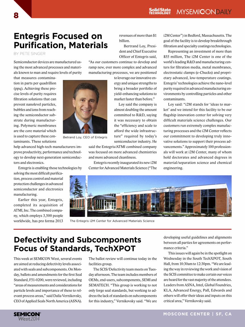
Entegris recently inaugurated its new i2M
Center for Advanced Materials Science (“The
i2M Center”) in Bedford, Massachusetts. The
goal of the facility is to develop breakthrough
filtration and specialty coatings technologies.
Representing an investment of more than
$55 million, The i2M Center is one of the
world’s leading R&D and manufacturing cen-
ters for filtration media, metal membranes,
electrostatic clamps (e-Chucks) and propri-
etary advanced, low-temperature coatings.
Entegris’ technologies achieve the nano-level
purity required in advanced manufacturing en-
vironments by controlling particles and other
contaminants.
Loy said: “i2M stands for ‘ideas to mar-
ket’ and we intend for this facility to be our
flagship innovation center for solving very
difficult materials science challenges. Our
customers run extremely complex manufac-
turing processes and the i2M Center reflects
our commitment to developing truly inno-
vative solutions to support their process ad-
vancements.” Approximately 100 profession-
als will work at i2M Center, many of whom
hold doctorates and advanced degrees in
material/separation science and chemical
engineering.
Entegris Focused on Purification, MaterialsBY PETE SINGER
The Entegris i2M Center for Advanced Materials Science
Betrand Loy, CEO of Entegris
Defectivity and Subcomponents Focus of Standards, TechXPOTThis week at SEMICON West, several events
are aimed at reducing defectivity levels associ-
ated with seals and subcomponents. On Mon-
day, ballots and amendments for the first Seal
Standard, F51-0200, were reviewed, including
“areas of measurements and considerations for
particle levels and importance of these to rel-
evant process areas,” said Dalia Vernikovsky,
CEO of Applied Seals North America (ASNA).
The ballot review will continue today in the
facilities group.
The SCIS/Defectivity team meets on Tues-
day afternoon. The team includes members of
OEMs, end-users, subcomponents, SEMI and
SEMATECH. “This group is working to not
only forge seal standards, but working to ad-
dress the lack of standards on subcomponents
for this industry,” Vernikovsky said. “We are
developing useful guidelines and alignments
between all parties for agreements on perfor-
mance criteria.”
This issues will again be in the spotlight on
Wednesday in the South TechXPOT, South
Hall, from 10:30am to 12:30pm. “We are lead-
ing the way in reviewing the work and vision of
the SCIS committee to make certain our voices
are heard for the vast majority of the attendees.
Leaders from ASNA, Intel, Global Foundries,
KLA, Advanced Energy, Pall, Edwards and
others will offer their ideas and inputs on this
critical area,” Vernikovsky said.
SHOW DAILY
WEDNESDAY | JULY 9, 2014
9SHOW DAILY
Fuji Electric expands power distribution portfolioFuji Electric announced that they have
added a product line-up to the MCCB/
ELCB portfolio. Fuji Electric has intro-
duced a new line of the MCCB/ELCB
of 32 to 63 AF. The G-Twin Lambda
Series feature a smaller design than
the existing breakers, making it an
ideal choice for machine equipment
and control panels. The new series’ key
features include footprint downsizing,
superior breaking capacity up to 18kA,
and compliance with international and
domestic standards.
Condensation Particle Counter for cleanroom applicationsParticle Measuring Systems’ Nano-ID
NPC10 is the first Condensation Par-
ticle Counter specifically developed for
cleanroom applications. The system
features a 2.8 LPM flow rate that does
not disrupt air flow and 10nm sensitivity,
which provides essential data for hard
disk manufacturing. It will also provide
quality control of ultra-fine nanopar-
ticle size distribution during synthesis,
air quality monitoring through detec-
tion of airborne ultra-fine and nanopar-
ticles in workplaces and other sensitive
environments, and exposure monitor-
ing by providing risk assessment of ex-
posure to airborne nano-objects and
exposure-dose relationships.
SCW14-ED_Jpn14_PQ.pdf 1 6/12/14 3:33 PM

MOSCONE CENTER | SF, CA
10
In 2004/2005, shipments of 300mm wafer fab
equipment (WFE) began to outpace that of
200mm platforms. As the “baton” in the node-
scaling race appeared to pass from 200mm to
300mm, it was clear that device manufactur-
ers were transitioning to higher-volume, more
cost-effective 300mm toolsets for cost efficien-
cies of the production of advanced memory
and microprocessor devices. Tool suppliers
enabled the transition with the availability of
the comprehensive 300mm toolset and began
a new 300mm technology race, and leaving the
major OEMs to focus on service and spares
for the now legacy 200mm toolsets. With
advanced device designs fully transitioned to
300mm, many IDMs and foundries were left
with growing excess capacity on their 200mm
production lines.
Surprisingly, new life and attention has
been refocused on the 200mm tool sets and
available capacity as two phenomena are driv-
ing new requirement and economics.
First, in 2006, a MEMS (Micro-Electro-
Mechanical Systems)-based accelerometer
became a game changer when introduced
into Nintendo’s next-generation Wii motion
controller. This was the first significant and
novel use of a MEMS device for motion track-
ing in a high-volume consumer application.
Next, in 2007, when Apple Inc. first introduced
the iPhone™ to the world, it came to light that
MEMS devices were enabling a number of its
advanced motion-based features.
Later, it would be noted that more than
75% of the semiconductor device content in
the iPhone was sourced from 200mm wafer
starts. The devices
manufactured on
2 0 0 mm wafer s
spanned a wide
variety of applica-
tions that included
not only MEMS ap-
plications (motion,
audio, RF, etc.) but
also CIS (CMOS
Image Sensor), com-
munications, power
management and
analog devices.
Sold in the hun-
dreds of millions
per year, first the
iPhone and then the multitude of other smart
phones, tablet PCs, and related digital de-
vices, that followed, drove the adoption of the
emerging “More-than-Moore” class of devices
(which were first pioneered on 150mm wafers
at the time) onto 200mm wafers. These high-
volume consumer applications gave rise to a
resurgence in both new and used of 200mm
equipment. This sudden requirement for new
sourcing of “legacy” 200mm toolsets placed
considerable strain on a supply chain that
then focused almost exclusively on 300mm;
tool vendors struggled in refurbishment, up-
grade, and production of matching tools and
processes that performed outside the require-
ments of traditional semiconductor applica-
tions (see Figure 1).
Some of these additional requirements
— including new and thicker films (>20µm),
advanced DRIE (Deep-Reactive-Ion-Etch) ca-
pabilities capable of delivering aspect ratios
approaching 100:1, and new process capabili-
ties like HFv (Hydrofluoric Acid vapor) release
etch and Wafer Bonding — resulted in OEMs
needing to restart 200mm tool development.
In some cases, OEMS needed to expand their
product portfolios to support the growing
needs of customers producing devices in the
rapidly expanding “More-than-Moore” device
segment.
Fast forward to 2014 —what a difference
approximately seven years has made to the
Figure 1. MEMS are considered one of the “More-than-Moore” class of emerging technology devices whose diversity presents consider-able challenge in process and materials capability to both device manufacturers and 200mm OEM providers alike. A challenge brought about by each device seemingly requiring its own unique enabling fabrication process or material.
Figure 2. The IoT (Internet-of-Things) by most accounts prescribes device volumes as high as 1 Trillion (per year!) by 2024. These device volumes are accompanied by severe reductions in ASP. Maintaining expanded device functionality, a reduced device size and a further reduced cost of fabrication, presents considerable challenge to both device producers and tool OEMs alike.
200mm Equipment Market Gaining New Lease on LifeSupporting Growth in Emerging Technologies
BY MIKE ROSA, APPLIED MATERIALS
continued on p 12

Join an exclusive group of influential executives involved in purchasing the total spectrum of equipment, materials and services necessary for semiconductor manufacturing.
Owned & Produced by: Presented by:
Solid State Technology’s Annual Conference & Networking Event
JOIN US AGAIN IN 2015!
Encore at the Wynn Las Vegas
May 19-22,
2015
BOOK YOUR SPONSORSHIP BY JULY 31st AND SAVE 15%
www.theconfab.com

MOSCONE CENTER | SF, CA
12
industry segment and more specifically the
number of opportunities in the 200mm WFE
market for the new class of devices.
The surge in mobile device applications and
more recently wear-
able technologies,
has meant that de-
vice manufacturers
are increasingly un-
der pressure to pro-
duce cheaper, small-
er, more capable and
more power efficient
devices most eco-
nomically and effi-
ciently — and this
remains optimally
on legacy 200mm
toolsets. Combining
this with the materi-
als and production
challenges presented by ultra-high volume
applications spelled out in the ‘Trillion Sensor
Vision’ and the now looming IoT (Internet-of-
Things) (see Figure 2), and it becomes clear that
OEMs who continue to support and develop so-
lutions for the 200mm WFE market have both
significant challenges and potential rewards.
Rising to the challenge presented by the
demands of these rapidly growing market seg-
ments, Applied Materials is an OEM that has,
over the past several years, continued to invest in
the R&D of its 200mm portfolio products. Chal-
lenged to deliver new materials and processes
(see Figure 3) in support the growing class of
200mm emerging technology applications that
have come to include MEMS, CIS, Power De-
vice, Analog, WLP (Wafer Level Packaging),
TFB (Thin Film Battery), and TSVs. Applied
Materials believes
that working close
to the customer and
more collaboratively
throughout the sup-
ply chain is para-
mount to success.
The 200mm eco-
system supporting
broadly expanding
cost-senstive device
classes represent a
new fork in the road-
map that has been
almost myopically
focused on Moore’s
Law evolution.
Learn more about how this dynamic mar-
ket is changing at the session on “Secondary
Equipment for Mobile & Diversified Applica-
tions.”
Future ICs will use more 3D device structures
such as finFETs and gate-all-around (GAA)
transistors, and so vacuum deposition pro-
cesses are needed that can produce confor-
mal films on the tops, bottoms, and side-walls
of features. New materials are needed as the
commercial IC fabrication industry pushes the
limits of device miniaturization, while industry
consolidation drives the remaining players to
use proprietary materials.
Even lithography needs more vacuum pro-
cessing when double-, triple-, and quadruple-
patterning schemes need sidewall spacer and
sacrificial hard-mask depositions. Materials
deposited in these process steps may not re-
main on the final chip, but they are nonetheless
essential in sub-22nm node process flows.
All of this leads to a need for an unprec-
edented number of new chemical precursors
for vacuum depositions to be simultaneously
ramped into high-volume manufacturing
(HVM) in fabs worldwide. “If you’re trying
to deposit a metal nitride, for example, four
different fabs may use four different precur-
sors sets,” explained Kate Wilson, global ap-
plications director, Edwards Vacuum Ltd. in
an exclusive interview with the Show Daily.
“With conformal processes, such as those
used for finFETs, there are a broad range of
processes needed,” continued Wilson. “The
solutions are diverging. For example, even if
you’re depositing silicon the number of pre-
cursors in use has probably tripled in the last
three years. We’re getting gas lists from end-
users with practically every metal precursor
possible, and if we ask which ones will be used
we’re told that all of them may be in use.”
Each molecular precursor has unique prop-
erties in terms of thermal stability, tendency to
polymerize, reactivity with oxygen, toxicity to
humans, and tendency to coat different mate-
rial surfaces. So each molecular precursor calls
for different solutions in vacuum processing
and effluent abatement. However, the same
precursor may be managed slightly differently
by different fabs in HVM.
Special ALD ChallengesAtomic Layer Deposition (ALD) can be con-
sidered as a special sub-set of chemical vapor
deposition (CVD), where the chemical precur-
sors are alternately pulsed into the vacuum
Figure 3. Leveraging its core capabilities in precision materials engineering, Applied Materials is able to deliver substantially re-engineered 200mm toolsets to produce advanced materials and processes needed to support the next generation of “More-than-Moore” devices. Source: Applied Materials
200mm continued from p 10
Vacuum Technologies Needed for 3D Device ProcessingComplex effluent management of ALD and CVD processes using novel precursors BY ED KORCZYNSKI
continued on p 14

The leader in covering semiconductor manufacturing and packaging technology, materials, products and news for over 50 years provides the same level of expertise and insides to decision makers for MEMS, displays, LEDs and power electronics manufacturing - in our magazine, seven e-Newsletter, comprehensive website and at The ConFab Conference and Networking event.
SEMICONDUCTORS
ADVANCED PACKAGING
MEMS
LEDS
DISPLAYS
POWER ELECTRONICS
Request your free subscription today, and see why electronics manufacturing professionals worldwide trust Solid State Technology
www.Solid-State.com

MOSCONE CENTER | SF, CA
14
chamber. The first ALD gas pulse coats device
features with a single layer of molecules, then
the second precursor pulse reacts with the mol-
ecules to leave behind a single layer of atoms.
ALD precursors are somewhat magical
molecules in terms of their properties. They
must completely coat the desired wafer sur-
faces, yet neither decompose nor polymerize
before reaching the wafer. They must remain
completely stable until reaching
the wafer surface, and then com-
pletely react to leave behind just
the atoms of choice. One com-
mon property of the precursors
molecules that include the atoms
of choice: to ensure near perfect
atomic coverage across 300mm
diameter wafers they tend to stick
to most other surfaces too.
ALD processing is a broad
topic, with known variations for
oxides, nitrides, metals, and ra-
re-earth elements. There are also
variations between thermally-ac-
tivated and plasma-enhanced pro-
cesses, but ALD generally occurs
in two different tools types: tube furnaces for
batch processing, and single-wafer chambers.
Tube furnace have large internal volumes, and
the alternating pulses of precursors occur on
a time-scale of minutes such that only one of
the two precursors flows through the tool at
any given time.
However, single-wafer ALD tools have small
internal volumes and precursor pulses occur-
ring on a time-scale of mere seconds, such that
the best process results derive from continuous
flows of both precursors through the tool. Gas
control manifolds are setup using high-speed
valves to divert flows to either the vacuum
chamber or directly to the exhaust stream.
For such processes, half the precursors are
shunted past the deposition chamber directly
to the exhaust, and the vacuum pump and
abatement system must handle not just process
effluent but high flows of unreacted precursors
that tend to stick to any surface.“You have to
consider dilution levels and side-reactions,”
cautioned Wilson. “Working with the OEM
and the end-users as they fine-tune these pro-
cesses is key to success.”
For some ALD process there are conflicting
challenges in configuring a vacuum solution,
such as one using a MOCVD precursors and a
chloride precursor. For the MOCVD molecule
the general approach would be to lower tem-
peratures to prevent decomposition, while for
the chloride molecule it would be best to use
high temperatures to prevent condensation.
Some molecules polymerize more at higher
temperatures, while condensing more at lower
temperatures, so a strategic trade-off must be
made.
“Chlorine-based precursors, for example,
are quite challenging to abate without creating
toxic by-products,” explained Wilson. “Most
of the things we abate become a powder, so we
have to deal with that powder to ensure that we
don’t clog the system.”
When ALD and conformal CVD processes
are used to form 3D structures in future sub-
22nm node ICs, there will be different thick-
nesses for the final films and different precur-
sors used in leading HVM lines. Consequently,
any standardization in vacuum technology
seems impossible, and a lot of customization
using proven sub-systems will be essential for
each end-user.
Vacuum and abatementDifferent fabs rely upon different overall vac-
uum strategies. In some cases there may be a
trade-off between capital costs and labor costs.
In some situations the solution may require
abatement of just perfluorocarbons (PFCs),
or may also require the abatement of toxics.
From fine-tuning of internal temperatures,
to modification of purge cycles, vacuum sys-
tem suppliers must work closely with OEMs
and end-users to ensure that everything has
been configured to work reliability in the final
system. Edward Vacuum starts by creating a
basic reference standard hardware-package
that’s flexible enough to work in general, and
then tailors it to fit each individual
situation.
“The OEM involvement is
becoming more key,” confided
Wilson. “The differentiation of
the process is more critical, and
we’re very involved with the OEM
in providing a complete solution.
We can’t test everything fully at
the OEM, but we establish perfor-
mance benchmarks that carry on
to the end-user.” Since low cost-
of-ownership is always desired,
coordination with the OEM al-
lows vacuum technologists to
keep hardware and dilutants gas
costs constrained by not over-
designing the system.
If the end-user works on an R&D line or
with a tool that has to process multiple IC
types, precursors in use may change from lot
to lot or from day to day. ALD/CVD vacuum
tools and abatement technologies must then
be flexible enough to safely and reliably deal
with a wide variety of precursors. With new
materials in use, not just deposition tools but
tools for etch and strip likewise need to be flex-
ible enough to properly handle a wider variety
of effluents than ever before.
A Temperature Management System (TMS)
on the foreline trap can be setup to take feed-
forward information from the OEM tool, allow-
ing for automated adjustment to different pre-
set modes appropriate for different precursors.
“We try not to use traps whenever possible,
because it introduces another potential failure
point and inevitable maintenance, but occa-
sionally it’s unavoidable,” elaborated Wilson.
Specifications from end-users for reliability
and uptime only become more challenging in
leading IC fabs.
Minimizing deposition in the system.
Vacuum Technologies cont’d from p 12

Need a Materials Partner witha Large Presence andBroad Capabilities?
It’s a Done Deal.With an increased global footprint, a broader portfolio of solutions and an impressive combined history of collaboration, innovation and support, Entegris and ATMI can now serve you as one, integrated team. From litho to cleans and etch to implant, no other materials supplier can offer more. Contact us to learn how the new Entegris can create a material advantage for you.
www.entegris.comEntegris®, the Entegris Rings Design®, Creating a Material Advantage®, ATMI® and the ATMI logo® are registered trademarks of Entegris, Inc.
©2014 Entegris, Inc. All rights reserved.

Go First Class: Go ClassOne.
If you work on 200mm or smaller substrates you don’t need to buy a big, expensive 300mm plating tool from the Big Guys. Because now there’s a smarter and much more a� ordable solution — called Solstice™. . . Solstice is a unique new electroplating tool that’s speci� cally designed for the world of smaller substrates. It gives you a cost-e� ective route from wet bench or development into volume production — and higher ROI!
Now: a cost-effective route to volume productionfor smaller-substrate applications...
Two Solstice models to choose fromSelect the Solstice LT for development — or the S8 for full cassette-to-cassette auto-mation, with touch-screen control, GEM/SECSII interface, full reporting and a great deal more. It will give you a major boost, not only in throughput — but also in quality, uniformity and reliability. So you can do more, and do it better, with fewer people.
First-class products from a new ClassOne company...In over a decade ClassOne Equipment has earned its reputation as the industry’s � rst-class provider of refurbished tools. Now a new sister company, ClassOne Technology, is extending the � rst-class tradition — creating innovative new tools to address important needs that have been underserved by the big manufacturers. So check out the new Solstice and see for yourself: It brings major new automation advantages without the big price tag. It really is “advanced plating for the rest of us!”
(406) 755-2200 • [email protected] West, Booth 511, South Hall
Solstice is a trademark of ClassOne Technology
INTRODUCING SOLSTICE: ADVANCED PLATINGFOR THE REST OF US!
Designed for 100-200MM apps. Half the Big Guys’ price!
ClassOne DailyNewsCov4.indd 1 6/19/14 11:24:16 PM