short-range ultra-wideband systems muri review agenda (afternoon)
TRANSCRIPT

Short-Range Ultra-Wideband Systems
UMass Antenna Lab USC UltRa Lab UC Berkeley BWRC
1:15 PM: Circuit DesignPanel: Bob Brodersen, Won Namgoong, Mike Chen, Ian O’Donnell, Stanley WangTopics: UWB Low Noise Amplifier Design in CMOS, low Power Integrated UWBTransceivers, CMOS Implementation Design for UWB Acquisition, Tracking and Detection
2:30 PM: Break2:40 PM: Future Goals
Topics: Fundamental Limits on Transient Radiation, UWB Arrays for Direction of Arrival Estimation, Control the UWB Waveform, Multipath-Embracing UWB Time Transfer and Location Techniques, Refined modeling/characterization of the UWB channel, UWB Performance and CMOS Impairments, Complete Asset Tracking System Panel: The UWB MURI Team
3:30 PM: Comments and questions from attendees4:00 PM: Evaluators' Meeting
MURI Review Agenda (Afternoon)

Short-Range Ultra-Wideband Systems
UMass Antenna Lab USC UltRa Lab UC Berkeley BWRC
Challenges in Digital UWB Receivers
• High-speed, high dynamic range ADC.– Parallel ADC required.
• Wideband LNA.
Jongrit Lerdworatawee, Ali Medi, Won Namgoong

Short-Range Ultra-Wideband Systems
UMass Antenna Lab USC UltRa Lab UC Berkeley BWRC
Time-Interleaved ADC
• ADC sees the full bandwidth of the input signal.– Sample/hold circuitry becomes difficult to design.– Sensitive to sampling jitter.
• Large dynamic range required in the presence of narrowband interferers.
Jongrit Lerdworatawee, Ali Medi, Won Namgoong

Short-Range Ultra-Wideband Systems
UMass Antenna Lab USC UltRa Lab UC Berkeley BWRC
Frequency Channelized ADC
• ADC input bandwidth reduced.– Sample/hold circuitry relaxed.– More robust to sampling jitter.
• Reduced dynamic range requirement.• Sampling jitter and mixer phase noise present.
Jongrit Lerdworatawee, Ali Medi, Won Namgoong

Short-Range Ultra-Wideband Systems
UMass Antenna Lab USC UltRa Lab UC Berkeley BWRC
No Narrowband Interferer
Jongrit Lerdworatawee, Ali Medi, Won Namgoong

Short-Range Ultra-Wideband Systems
UMass Antenna Lab USC UltRa Lab UC Berkeley BWRC
Narrowband Interferer Present
Jongrit Lerdworatawee, Ali Medi, Won Namgoong

Short-Range Ultra-Wideband Systems
UMass Antenna Lab USC UltRa Lab UC Berkeley BWRC
Implementation of Channelized Receiver
• A 2-channel LNA/mixer in 0.25um CMOS is currently in fabrication.
• A multi-output frequency synthesizer has been design.
1 GHzRef.Freq.
Active loopFilter
4 GHzOutput
VCO
Poly-PhaseFilter
VCDILFD
12
Active loopFilter
5 GHzOutput
VCO
Poly-PhaseFilter
Active loopFilter
6 GHzOutput
VCO
Poly-PhaseFilter
Active loopFilter
7 GHzOutput
VCO
Poly-PhaseFilter
Jongrit Lerdworatawee, Ali Medi, Won Namgoong

Short-Range Ultra-Wideband Systems
UMass Antenna Lab USC UltRa Lab UC Berkeley BWRC
Research on UWB LNA
1. Understand tradeoffs between LNA gain and NF for wideband signals.– Redefine noise figure.– Generalize noise analysis of 2-port network.– Develop a systematic design methodology for
wideband LNA.2. LNA implementation.
Jongrit Lerdworatawee, Ali Medi, Won Namgoong

Short-Range Ultra-Wideband Systems
UMass Antenna Lab USC UltRa Lab UC Berkeley BWRC
Noise Figure
• Formal definition introduced by Friis (1940s).– NF = (input SNR)/(output SNR).– Measures degradation in the SNR as signal passes through
the receiving system.• SNR defined at an infinitesimal frequency band.
– How do you measure SNR when noise is colored?
Jongrit Lerdworatawee, Ali Medi, Won Namgoong

Short-Range Ultra-Wideband Systems
UMass Antenna Lab USC UltRa Lab UC Berkeley BWRC
Meaningful NF Metric
• Goal of a receiving system in a digital receiver is to condition the received analog signal for digitization. – Achieve highest performance after decoding in digital domain.
• SNR should measure performance after the digital decoding process.– Metric for a single block, not the entire system.
• Define SNR as the MFB.– Achievable performance after digital decoding.– NF measures the degree of degradation in the achievable receiver
performance.
Jongrit Lerdworatawee, Ali Medi, Won Namgoong

Short-Range Ultra-Wideband Systems
UMass Antenna Lab USC UltRa Lab UC Berkeley BWRC
Effective Noise Figure
• Effective NF obtained by defining the SNR as the MFB.• The effective NF becomes
• Analogous to
• Effective resistance of parallel resistors is dominated by the smaller resistors.– Suggests spot NF can be increased in some frequencies for
implementation benefits with little loss in performance.
Jongrit Lerdworatawee, Ali Medi, Won Namgoong

Short-Range Ultra-Wideband Systems
UMass Antenna Lab USC UltRa Lab UC Berkeley BWRC
LNA Gain and NF Tradeoff
• Design matching network to optimally trade effective NF with transducer gain.
• Need to analyze noise and gain tradeoff systematically using 2-port network analysis. • Problematic in several common CMOS LNA
architectures (e.g., inductor degeneration).
Jongrit Lerdworatawee, Ali Medi, Won Namgoong
Short-Range Ultra-Wideband Systems
UMass Antenna Lab USC UltRa Lab UC Berkeley BWRC
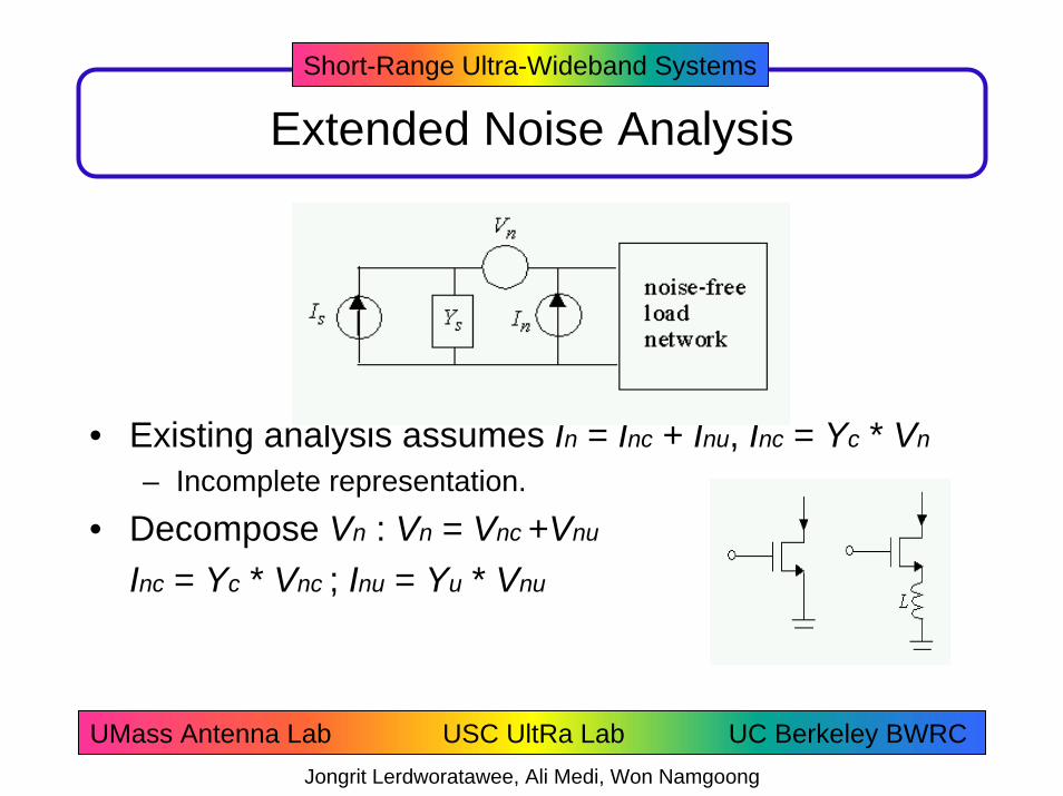
Extended Noise Analysis
• Existing analysis assumes In = Inc + Inu, Inc = Yc * Vn
– Incomplete representation.
• Decompose Vn : Vn = Vnc +Vnu
Inc = Yc * Vnc ; Inu = Yu * Vnu
Jongrit Lerdworatawee, Ali Medi, Won Namgoong

Short-Range Ultra-Wideband Systems
UMass Antenna Lab USC UltRa Lab UC Berkeley BWRC
NF circle
G circle
Optimal Matching Network
• At every frequency, optimal gain/NF obtained graphically.
• For wideband matching, solve constrained optimization problem.– Minimize effective NF subject to average
gain over a frequency band of interest.– Assume no structure to solve the lower bound.
• Quantify effectiveness of various matching structures.
• Currently applying these techniques to design LNA for 3-10GHz.
Jongrit Lerdworatawee, Ali Medi, Won Namgoong

Short-Range Ultra-Wideband Systems
UMass Antenna Lab USC UltRa Lab UC Berkeley BWRC
LNA Implementation (in fabrication)
M1
Vdd
Vin M2
M3
Vdd
Vb Vout
MatchingNetwork
For simplicity, biasing is not shown here.
Simulation Results
• Matching Bandwidth:(S11 < -10dB) 2.16 – 4.75GHz
• Overall Gain: 15.5 – 12.9 dB
• Noise Figure: 4.5 – 4.4 dB
• IIP3: 6.1 dBm
• Power Supply: 2 Volts
• Power Dissipation: 40 mW
• Technology: TSMC 0.25μm
Jongrit Lerdworatawee, Ali Medi, Won Namgoong

Short-Range Ultra-Wideband Systems
UMass Antenna Lab USC UltRa Lab UC Berkeley BWRC
Implementation Research Projects
• Real-time UWB prototyping infrastructure (Bob)– Implementation of BEE FPGA array– First pass at UWB front-end
• Implementation of Ultra Low Power - Ultra Wide Band (ULP-UWB) CMOS transceiver– System design and simulation on BEE – Flexible architecture
• Variable data rates• Programmable codes
– Analog– 2 Gbit/sec A/D– Antenna/CMOS LNA
– Fully parallel digital baseband chip design (Mike)
Bob Brodersen

Short-Range Ultra-Wideband Systems
UMass Antenna Lab USC UltRa Lab UC Berkeley BWRC
Implementation strategies (baseband)
Simulink/Stateflow Description
ASIC Implementation“Chip in a day”
BEEFPGA Array
Bob Brodersen

Short-Range Ultra-Wideband Systems
UMass Antenna Lab USC UltRa Lab UC Berkeley BWRC
Processing Board PCB
• Board Dimension: 53 X 58 cm• Layout Area: 427 sq. in.• No. of Layers: 26
• Computation rate – 600 Billion ops/sec
• 1600 I/O connections• Board-level Main Clock Rate:
160MHz+• On Board connection speed:
– FPGA to FPGA: 100MHz– XBAR to XBAR: 70MHz
Bob Brodersen

Short-Range Ultra-Wideband Systems
UMass Antenna Lab USC UltRa Lab UC Berkeley BWRC
BEE in Chassis with I/O
Bob Brodersen

Short-Range Ultra-Wideband Systems
UMass Antenna Lab USC UltRa Lab UC Berkeley BWRC
BEE UWB I/O (block diagram)
4-poleButterworth
LPFFc=550MHz
4-poleButterworth
LPFFc=550MHz
LNA/VGA ADC
x15
2 8
3HD-SCSI
Connectors 120
ToBEE
16dB-26dB Gain Control Range
1.244GHzPLL
1:20PECL
Clock Driver
PECL to
LVDS1:4
22
DATA_READY bit from ADCis used to clock deserializers at622MHz622MHz.
1:2 outputdemux of ADC provides two parallel 8-bitPECL outputs at 622MHz622MHz. (We use the upper 7-bits.)
The output linesof the deserializersoperate at 155MHz155MHz.
60-bits in LVDSformat are sent at 155MHz155MHz across 120 wires through 3 HD-SCSI connectors to the BEE.
12MHzcrystal ref.
PECLDelay
(10ps resolution)
2Note: The programmable delay is needed to properly position the clock relative to the data transitions, so that no setup or hold time violations will occur at the input registers of the deserializers.
1:4 impedance
ratio
LNA/VGA
Bob Brodersen

Short-Range Ultra-Wideband Systems
UMass Antenna Lab USC UltRa Lab UC Berkeley BWRC
Transceiver PCBPower Supply Regulators
+5V Analog -5V Analog
+5V Digital
+3.3V Digital
ADCPECL Delay
1:20 PECLClock Driver
PLLLVDS Receivers
Tx Chip
PECL to LVDS1:4 Deserializers
Ref.
LNA/VGA
4-pole Butterworth LPF
68-pin HDSCSI connector
68-pin HDSCSI connector
68-pin HDSCSI connector
Bob Brodersen

Short-Range Ultra-Wideband Systems
UMass Antenna Lab USC UltRa Lab UC Berkeley BWRC
Prototyping Hardware Status
• BEE operational and in use for verification of digital baseband circuitry
• First pass of UWB transceiver completed and second version in design– Increasing bandwidth to 1 GHz (2.4 Gbit/sec A/D
conversion) – Using fiber links between BEE and analog
transceiver • Electrical isolation• Higher digital bandwidth (20 Gbits/sec)
Bob Brodersen

Short-Range Ultra-Wideband Systems
UMass Antenna Lab USC UltRa Lab UC Berkeley BWRC
Chip implementation
• Digital design verified in BEE• Analog design completed and beginning
layout
Remaining talks on this activity:– Ian: Chip architecture and critical design issues– Stanley: LNA and pulser– Mike: Digital baseband design
Bob Brodersen

Short-Range Ultra-Wideband Systems
UMass Antenna Lab USC UltRa Lab UC Berkeley BWRC
UWB Integrated Transceiver Project
Specifications:• 100kbps over 10m with
10-3 BER • 1mW total (TX+RX)
power consumption• 0-1GHz bandwidth
First All-CMOS Integrated UWB TransceiverAggressive Low-Power Design
“Mostly-Digital” approach, simplify analog front-endProvide Flexible Platform for Further Research
Targeting Sensor Network Application
GAIN
TX
CLK
ADC
DIG
ITA
L
Ian O'Donnell, Bob Brodersen

Short-Range Ultra-Wideband Systems
UMass Antenna Lab USC UltRa Lab UC Berkeley BWRC
Transceiver Operation
time
time
TSAMPLE
TWINDOW
TPULSE_REP
Parallel Sampling of a Window of Time
TSYMBOL
Ian O'Donnell, Bob Brodersen

Short-Range Ultra-Wideband Systems
UMass Antenna Lab USC UltRa Lab UC Berkeley BWRC
UWB Transceiver Architecture
LNA
PULSE
GAIN andFILTERING
A/DS/H
A/DS/H
A/DS/H
PMF
Data Recovery
SynchDetectAnd
Tracking
CLK GENCONTROL
Ian O'Donnell, Bob Brodersen

Short-Range Ultra-Wideband Systems
UMass Antenna Lab USC UltRa Lab UC Berkeley BWRC
Performance: Throughput/Power
Published Results:
< 10 kbps/mWFor ~10m
100 kbps/mW
10 kbps/mW
1 kbps/mW
CMOS UWB
Potentially10x Better
Ian O'Donnell, Bob Brodersen

Short-Range Ultra-Wideband Systems
UMass Antenna Lab USC UltRa Lab UC Berkeley BWRC
Mapping UWB to Hardware
Quantify Effects of Hardware Impairments:• Analog to Digital Conversion Bitwidth• Matched Filter and post-Correlation sizes• Timing Requirements:
• Precision (Matching between TX and RX)• Accuracy (Jitter)
A/DS/H
A/DS/H
A/DS/H
PMF
CLK GEN
Ian O'Donnell, Bob Brodersen

Short-Range Ultra-Wideband Systems
UMass Antenna Lab USC UltRa Lab UC Berkeley BWRC
A/D Sampling Bitwidth
1-bit A/DIs Adequate
Ian O'Donnell, Bob Brodersen

Short-Range Ultra-Wideband Systems
UMass Antenna Lab USC UltRa Lab UC Berkeley BWRC
Matched Filter Tap Bitwidth
5-bit CoefficientsAre Adequate
Ian O'Donnell, Bob Brodersen

Short-Range Ultra-Wideband Systems
UMass Antenna Lab USC UltRa Lab UC Berkeley BWRC
Oscillator Accuracy (Matching)
Crystal
10 PPM
0.1%1000 PPM
10%
PrecisionComponent
TCXO
For:Drift < 100ps Over
Symbol
Crystal is Required
20 MHz
200 kHz
2 GHz
Ian O'Donnell, Bob Brodersen

Short-Range Ultra-Wideband Systems
UMass Antenna Lab USC UltRa Lab UC Berkeley BWRC
Oscillator Precision (Jitter)
Ring Oscillators
LC Oscillators
For:RMS
Jitter < 25ps Over
Symbol
Crystal is GoodCrystal Oscillators
-90 dBc/Hz@ 0.1% of fc
-120 dBc/Hz@ 0.1% of fc
1.6 MHz
Ian O'Donnell, Bob Brodersen

Short-Range Ultra-Wideband Systems
UMass Antenna Lab USC UltRa Lab UC Berkeley BWRC
UWB CMOS Transceiver Status
Status:System Design CompleteAnalog Circuit Design CompleteDigital Design Complete and in
Verification Stage
To Do:Analog LayoutMerge Analog/Digital into
Single DieTop-level testing
Tape-out in next couple months.
Ian O'Donnell, Bob Brodersen

Short-Range Ultra-Wideband Systems
UMass Antenna Lab USC UltRa Lab UC Berkeley BWRC
Introduction
• Pulse generator and low-noise amplifier are circuits interfacing with antennas
• Basic properties of UWB antennas have to be known
Stanley Wang, Bob Brodersen

Short-Range Ultra-Wideband Systems
UMass Antenna Lab USC UltRa Lab UC Berkeley BWRC
• For indoor wireless applications, antennas have to be small
• Small antennas have simple equivalent circuits
• Curve-fitting the input impedance– Only ONE RESISTOR
• Use the terminal voltages to help design the driver/LNA
E-Field
Rrad+
-
Vin
+
-
SmallLoop Antenna
Small Loop Antenna Example
Stanley Wang, Bob Brodersen

Short-Range Ultra-Wideband Systems
UMass Antenna Lab USC UltRa Lab UC Berkeley BWRC
• Large Current Radiator (LCR) as the TX antenna
• Low-pass filter for pulse-shaping & FCC radiation mask
Pulser
• H-bridge pulser to drive inductive load
• Flexible driving force by parallel structure
UWB Pulse Generation
Stanley Wang, Bob Brodersen

Short-Range Ultra-Wideband Systems
UMass Antenna Lab USC UltRa Lab UC Berkeley BWRC
H-bridge Operations (Transmit ‘0’)• EP0 & EN0 turned on • Current flows from Vdd to
Gnd thru LCR• Fast-rising voltage at LCR
terminals generates a positive Gaussian pulse
• EN0 off and EP0 on• Current flows back to Vdd• Fast-falling voltage at LCR
terminals generates a negative Gaussian pulse
Stanley Wang, Bob Brodersen

Short-Range Ultra-Wideband Systems
UMass Antenna Lab USC UltRa Lab UC Berkeley BWRC
0 0.5 1 1.5-120
-110
-100
-90
-80
-70
-60
0 2 4 6 8 10 12-0.1
-0.08
-0.06
-0.04
-0.02
0
0.02
0.04
0.06
0.08
0.1
• Intervals of doublets affects the width of the frequency lobes, but total power radiated keeps the same
• The smaller the interval, the smaller the power consumption and higher the efficiency
Time(ns) Frequency (GHz)
VRrad
Low-Power Pulse Generator Design
Stanley Wang, Bob Brodersen

Short-Range Ultra-Wideband Systems
UMass Antenna Lab USC UltRa Lab UC Berkeley BWRC
• Waveform of the source imitates the radiated E-field
• Source impedance equal to antenna input impedance
• LNA Matching Network
LNA
UWB Receiver Front-end
Stanley Wang, Bob Brodersen

Short-Range Ultra-Wideband Systems
UMass Antenna Lab USC UltRa Lab UC Berkeley BWRC
• Specifications– Fully-differential for on-chip interference immunity– Voltage Gain > 15dB – 3dB BW : 0.1~1GHz– NF < 6dB– Linearity : doesn’t matter– Constant group delay– Input impedance : 50ohm– Goal : Minimize power consumption (< 1mW)
• Low input impedance sets the power consumption • What LNA topology should be used?
LNA
ZLNA
Sub-mW UWB LNA Design
Stanley Wang, Bob Brodersen

Short-Range Ultra-Wideband Systems
UMass Antenna Lab USC UltRa Lab UC Berkeley BWRC
Existing Wideband LNA
• Resistive-terminated LNA has very bad NF• Shunt-FB and CG LNA’s need gm = 40mA/V which makes
sub-mW power consumption unfeasible
Shunt-Feedback Common-GateR-terminated
Rin = RT Rin = 1/gmRin = Rf/(1+gmRL)
Vb1
Vout
RL
Vin
Stanley Wang, Bob Brodersen

Short-Range Ultra-Wideband Systems
UMass Antenna Lab USC UltRa Lab UC Berkeley BWRC
Current-Reuse Technique• PMOS are added in
as amplifying devices
• No extra DC current• Gm = gmn + gmp
• Rin is halved• Voltage gain is
doubled• NF decreased by
3dB• BW decreased but
OK• Still burn > 1mW
Shunt-Feedback
Rin = 1/(gmn+gmp)Rin,diff = 2/(gmn+gmp)
Vin
Common-Gate
Vout
VbngmnVin
gmpVin
Cc1
Cc2
Vbp
Vin Vout
gmnVin
gmpVin
Rin = 1/(gmn+gmp)Rin,diff = 2/(gmn+gmp)
Stanley Wang, Bob Brodersen

Short-Range Ultra-Wideband Systems
UMass Antenna Lab USC UltRa Lab UC Berkeley BWRC
FB/CG Hybrid LNA
• Mp1/Mn1/Rf1act as FB Amp to Vin+ and CG Amp to Vin-
• Mp2/Mn2/Rf2 act as FB Amp to Vin- and CG Amp to Vin+
• Rin = 1/ [ 2*(gmn+gmp)]For Rin = 50ohm, gmn = gmp = 5mA/V
8 times smaller than 40mA/V in CG or Shunt-FB amplifier!
sub-mW LNA feasible• Av = 2*(gmn+gmp)*Rf
Stanley Wang, Bob Brodersen

Short-Range Ultra-Wideband Systems
UMass Antenna Lab USC UltRa Lab UC Berkeley BWRC
102
103-20
-15
-10
-5
0
5
10
15
20
• Back-gate Cross-coupling enhances Gm by 10%
dB
Frequency(MHz)
NF
s11
Av
• Power = 0.61mW• All the specs are met
LNA Schematic & Simulation
Stanley Wang, Bob Brodersen

Short-Range Ultra-Wideband Systems
UMass Antenna Lab USC UltRa Lab UC Berkeley BWRC45um
59um
Mb1Mb2
Mb3Mb4
Mp1
Mp1 Mp2
Mp2
Mn2
Mn2
Mn1
Mn1
Rf1Rf2
• ST Microelectronics 0.13um CMOS triple-well process
• Layout area: 59um x 45um
• Common-centroid layout for good transistor matching
• Dummy for good resistor matching
• Capacitors not shown
UWB LNA Layout
Stanley Wang, Bob Brodersen

Short-Range Ultra-Wideband Systems
UMass Antenna Lab USC UltRa Lab UC Berkeley BWRC
Why Dedicated ASIC for UWB?
0.01
0.11
10
1001000
10000PP
C-95
PPC1
-SO
I-00
Spar
c-95
Spar
c2-9
7PP
C2-S
OI-0
0Sp
arc1
-97
X86-
97Alp
ha-0
0Alp
ha-9
7PP
C-00
SA-D
SP-9
8H
it-D
SP-9
8Fu
j-DSP
2-98
Fuj-D
SP1-
00N
EC-D
SP-9
8M
PEG
2-99
Encr
ypt-0
0M
UD-9
8M
PEG
2-98
802.1
1a-0
1UW
B-03
MO
PS/m
W
DedicatedGeneral Purpose
DSP
Microprocessors
Here we are!
Mike Chen, Bob Brodesen

Short-Range Ultra-Wideband Systems
UMass Antenna Lab USC UltRa Lab UC Berkeley BWRC
What does Baseband do?• Fuctionality:
acquisition; ML detection; early/late tracking
• Target: sufficient flexibility & low power!
• Pulse Repetition (Clocking) Rate:30 MHz to 1 MHz
• Maximum Raking Length(Trake=Tpulse+Tspread): < 64ns (128 samples)
• Additional Processing Gain0 to 30 dB
Mike Chen, Bob Brodesen

Short-Range Ultra-Wideband Systems
UMass Antenna Lab USC UltRa Lab UC Berkeley BWRC
Baseband Chip Diagram
Coef
160
128
PN correlator 1
PN correlator 2
PN correlator 32
CLK
PN GenCLKcoef
CLKpn
AbsPeakDet
DataRecover
(soft/hard)
Controllogic
Correlation_Block
Data_out
SymbolStrobe
DataPN
Correlator
PCI
DEC
CLKwin
S/P32
PMF 1
PMF 2
PMF 32
Matched FilterBank
Mike Chen, Bob Brodesen

Short-Range Ultra-Wideband Systems
UMass Antenna Lab USC UltRa Lab UC Berkeley BWRC
Flexible Low Power Architecture
• Fully parallel matched filter (FIR), and PN correlator structuresHigh area and power efficiency without time multiplexing
• Ability to turn down the unused transistors for 10x power savingin tracking mode
• Programmable matched filter response and PN codes
• Duty-cycled and continuous operation modes
Mike Chen, Bob Brodesen

Short-Range Ultra-Wideband Systems
UMass Antenna Lab USC UltRa Lab UC Berkeley BWRC
Parallel v.s. Serial Searching Scheme
•Assume 1024 PN chips, 10 MHz pulse rate.
(1) Acquisition Time (2) Area Cost
Fully Parallel (0.4 ms)
Serial (0.4sec)
Fully Parallel (500 mm2)
Serial (5.8 mm2)
Mike Chen, Bob Brodesen

Short-Range Ultra-Wideband Systems
UMass Antenna Lab USC UltRa Lab UC Berkeley BWRC
Design Methodology
• Develop algorithm in Matlab/Simulink, BEE and ASIC implementations start from Simulink netlist.
• Datapath is synthesized and explored in Module Compiler.
• Control logic is designed in StateFlow, and later translated by SF2VHD.
• Massive parallel and structured processing elements requires 31 meters of wires!
Hierarchical front end and physical design.
Mike Chen, Bob Brodesen

Short-Range Ultra-Wideband Systems
UMass Antenna Lab USC UltRa Lab UC Berkeley BWRC
Design Flow
Develop Algorithm Backend Physical DesignFront End Design Verification
XSG
Matlab Test Vector
Top-level VHDL
Synthesis & Optimization:Design Compiler
IncrementalCompile
Gate VerilogGate VHDL
Modelsim
FP & Place:First Encounter
Power Strap Cmd
HierarchyPlacement
DEF
Final VerilogRoute:Nanoroute
GDS
GDS
Design Spice
CDL for ST lib.
Calibre DRC/Antenna Rule
EPIC VerifySTA -> Path Mill
Func, Power -> Nanosim
SPF/SDF/set_load
Filler Spice
CDL netlist
custom antennaLEF files
Bottom Up/ TopDown hierarchies
Algorithmic:Simulink
Schematic
BEE
ModuleCompiler
State FlowSF2VHD
Gate VHDL
Behavioral VHDL
End of FE
End of FE
Calibre LVS
OpusSwitch I/O cell viewSwitch fillter cellToplevel pin text
VCD
VCD
Mike Chen, Bob Brodesen

Short-Range Ultra-Wideband Systems
UMass Antenna Lab USC UltRa Lab UC Berkeley BWRC
Graphic View of Flow
Mike Chen, Bob Brodesen

Short-Range Ultra-Wideband Systems
UMass Antenna Lab USC UltRa Lab UC Berkeley BWRC
UWB Baseband Chip Status
Process: 0.13um (ST Microelectronics)Size: 3.6mm x 3.3mm Standard Cells: 530,000MOPS/mW: 1,483Power:Acquisition 12 mW Tracking 1.5 mW
@ 1.08 V, 10 MHz clk
Mike Chen, Bob Brodesen

Short-Range Ultra-Wideband Systems
UMass Antenna Lab USC UltRa Lab UC Berkeley BWRC
1:15 PM: Circuit DesignPanel: Bob Brodersen, Won Namgoong, Mike Chen, Ian O’Donnell, Stanley WangTopics: UWB Low Noise Amplifier Design in CMOS, low Power Integrated UWB Transceivers, CMOS Implementation Design for UWB Acquisition, Tracking and Detection
2:30 PM: Break2:40 PM: Future Goals
Topics: Fundamental Limits on Transient Radiation, UWB Arrays for Direction of Arrival Estimation, Control the UWB Waveform, Multipath-Embracing UWB Time Transfer and Location Techniques, Refined modeling/characterization of the UWB channel, UWB Performance and CMOS Impairments, Complete Asset Tracking System Panel: The UWB MURI Team
3:30 PM: Comments and questions from attendees4:00 PM: Evaluators' Meeting
MURI Review Agenda (Afternoon)