shift instructions (1/4) °move (shift) all the bits in a word to the left or right by a number of...
Post on 21-Dec-2015
224 views
TRANSCRIPT
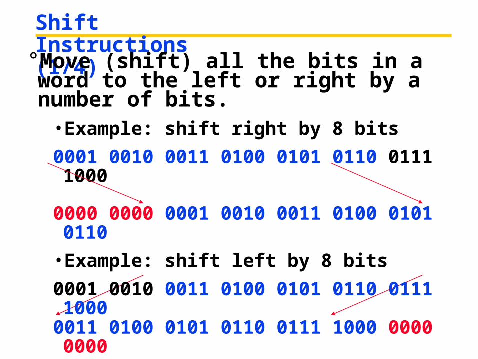
Shift Instructions (1/4)
°Move (shift) all the bits in a word to the left or right by a number of bits.
• Example: shift right by 8 bits
0001 0010 0011 0100 0101 0110 0111 1000
0000 0000 0001 0010 0011 0100 0101 0110
• Example: shift left by 8 bits
0001 0010 0011 0100 0101 0110 0111 1000
0011 0100 0101 0110 0111 1000 0000 0000

Shift Instructions (2/4)° MIPS Shift Instruction Syntax:
1 2,3,4• where
1) operation name2) register that will receive value3) first operand (register)4) shift amount (constant < 32, 5 bits)
° MIPS shift instructions:1. sll (shift left logical): shifts left and fills empt
ied bits with 0s2. srl (shift right logical): shifts right and fills e
mptied bits with 0s3. sra (shift right arithmetic): shifts right and fill
s emptied bits by sign extending

Shift Instructions (3/4)°Example: shift right arith by 8 bits
0001 0010 0011 0100 0101 0110 0111 1000
0000 0000 0001 0010 0011 0100 0101 0110
°Example: shift right arith by 8 bits1001 0010 0011 0100 0101 0110 0111 100
01111 1111 1001 0010 0011 0100 0101 0110

Shift Instructions (4/4)°Since shifting may be faster than mul
tiplication, a good compiler usually notices when C code multiplies by a power of 2 and compiles it to a shift instruction:a *= 8; (in C)would compile to:sll $s0,$s0,3 (in MIPS)
°Likewise, shift right to divide by powers of 2
• remember to use sra

“Shift and Add” Signed Multiplier
Bn-bit shift registers
P
An-bit register
+0
10
n-bit adder
• Signed extend partial product at each stage
• Final step is a subtract
• n-clock cycles

Fast multiplication hardware

Chap.5 The processor: Datapath and control
Jen-Chang Liu, Spring 2006

Hierarchy of Machine Structures
I/O systemProcessor
Compiler
Operating
System(Windows 98)
Application (Netscape)
Digital Design
Circuit Design
Instruction Set Architecture
Datapath & Control
transistors
MemoryHardware
Software Assembler

Five components of computer
Input, output, memory, datapath, control

Inside Mother board (for Pentium Pro)
FourISAcardslots
FourPCIcardslots Four
SIMMslots
Two IDEconnectors
Processor
Parallel/serial
Audio/MIDI

Chapter overview Chap5: datapath and control Chap6: pipeline Chap7: memory hierarchy Chap8: I/O Chap9: multiprocessor
InsideCPU

Inside Processor: datapath and control
Datapath: brawn of the processor Perform the arithmetic operations
Control: brain of the processor Tells the datapath, memory, and I/O what to d
o
生產線

Branch
Control
Datacache
Instructioncache
Bus Integerdata-path
Floating-point
datapath
Inside Pentium Processor
1/3 cache

Inside Pentium Pro Processor
Branch
Instructioncache andfetch unit Instruction
decodeMicrocode(control)
Reorder buffer(control)
Reservation stations(control)
Memorybuffer
I/O unit
Data cache
Integerdata- path
Floating-point
datapath

Clocks methodology
Clock period Rising edge
Falling edge
high
low
Edge-triggered clocking: the content of the state elements (flip-flops, registers, memory) only change on the active clock edge
Clock cycle
Stateelement
1Combinational logic
Stateelement
2
100 101 001 111
100 110 001

Timing constraint The clock period must be long
enough to allow signals to be stable
Flip-flopCombinational
logic blockFlip-flop
D
C
tprop tcombinational tsetup
Q D
C
Q

Design Target: MIPS The instruction set architecture (ISA) de
termines the implementation We know how to execute MIPS codes m
anually, how to design a circuit to execute them?
We design a simple implementation that includes a subset of MIPS inst. Memory-reference inst.: lw, sw Arithmetic-logic inst.: add,sub,and,or,slt Branch: beq, j

Outline of chapter 5 Building a datapath
Instruction fetch R-type instructions Load/store Branch
Single Datapath implementation Multiple cycle implementation

Preview: How to carry out an instruction 4 steps to implement an
instruction執行
Instructionfetch
Data/registerread
Instructionexecution
Memory/registerread/write
add $t0, $t1, $t2
lw $t0, 0($a0)
beq $t0, $t1, loop
$t1, $t2
$a0
$t0, $t1
ALU
$t1 + $t2
$a0 + 0
$t0 - $t1
Write to $t0
Read from memory
Write PC
Read inst.from memory

Abstract view of carrying out an instruction
Registers
Register #
Data
Register #
Datamemory
Address
Data
Register #
PC Instruction ALU
Instructionmemory
Address
Instructionfetch
Data/registerread
Instructionexecution
Memory/registerread/write

How to build datapath for MIPS ISA?
Datapath: path to perform an instruction Consider each major components Build datapath for each instruction class
Registers
Register #
Data
Register #
Datamemory
Address
Data
Register #
PC Instruction ALU
Instructionmemory
Address

Outline Building a datapath
1. Instruction fetch2. R-type instructions3. Load/store4. Branch
Build datapath foreach instruction class,then combine them

1. Instruction fetch
PC
Instructionmemory
Instructionaddress
Instruction
a. Instruction memory b. Program counter
Add Sum
c. Adder
Place to storethe instructions
Address of theinstructions
Increment thePC to nextinstruction

Instruction fetch (cont.)
PC
Instructionmemory
Readaddress
Instruction
4
Add
12
3always adds,therefore nocontrol lines
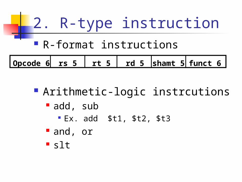
2. R-type instruction R-format instructions
Arithmetic-logic instrcutions add, sub
Ex. add $t1, $t2, $t3 and, or slt
Opcode 6 rs 5 rt 5 rd 5 funct 6shamt 5

Datapath elements for R-type inst.
ALU control
RegWrite
RegistersWriteregister
Readdata 1
Readdata 2
Readregister 1
Readregister 2
Writedata
ALUresult
ALU
Data
Data
Registernumbers
a. Registers b. ALU
Zero5
5
5 3
1. Read register: read register no., output data
2. Write register: write register no., input data, RegWrite=1
input output
4

Datapath for R-type inst.
InstructionRegisters
Writeregister
Readdata 1
Readdata 2
Readregister 1
Readregister 2
Writedata
ALUresult
ALU
Zero
RegWrite
ALU operation3
1
Opcode 6 rs 5 rt 5 rd 5 funct 6shamt 5
2
3
4

3. Load/store from/to memory I-format
Load/store examples lw $t1, offset_value($t2) sw $t1, offset_value($t2)
Opcode 6 rs 5 rt 5 Signed offset 16
…
$t2
offset

Datapath elements for load/store Register file, ALU, and data
memory
16 32Sign
extend
b. Sign-extension unit
MemRead
MemWrite
Datamemory
Writedata
Readdata
a. Data memory unit
Address
Sign-extend the 16-bitoffset field
Store -> MemWriteLoad -> MemRead
Base+offset
lw $t1, offset_value($t2)

Datapath for load/store
Instruction
16 32
RegistersWriteregister
Readdata 1
Readdata 2
Readregister 1
Readregister 2
Datamemory
Writedata
Readdata
Writedata
Signextend
ALUresult
ZeroALU
Address
MemRead
MemWrite
RegWrite
ALU operation3
1
2
Opcode 6 rs 5 rt 5 Signed offset 16
4

4. Branch I-format
Example beq $t1, $t2, offset PC-relative addressing
Opcode 6 rs 5 rt 5 Signed offset 16

Details for branch: target address calculation Base address for offset: PC+4
Instructions are word-aligned: the offset is shifted left 2 bits
…
PC+4
Opcode 6 rs 5 rt 5 Immediate 16
offset 00
offset

Datapath for branch
16 32Sign
extend
ZeroALU
Sum
Shiftleft 2
To branchcontrol logic
Branch target
PC + 4 from instruction datapath
Instruction
Add
RegistersWriteregister
Readdata 1
Readdata 2
Readregister 1
Readregister 2
Writedata
RegWrite
ALU operation3
1
2
Opcode 6 rs 5 rt 5 Signed offset 16
4

How to combine these datapaths ? We have shown datapaths for
Instruction fetch R-type instructions Load/store branch
How to assemble the datapaths? How to handle control lines?

Outline Building a datapath
Instruction fetch R-type instructions Load/store Branch
Single Datapath implementation Multiple cycle implementation

Single datapath implementation
Attempt to execute all instructions in 1 clock cycle
No datapath resources can be used more than once per instruction Duplicated units: ex. Memory for instructions and
memory for data Shared units: use multiplexor to select input
add,…
lw, sw
beq,…
生產線

1. Combine R-type and lw/swInstruction
RegistersWriteregister
Readdata 1
Readdata 2
Readregister 1
Readregister 2
Writedata
ALUresult
ALU
Zero
RegWrite
ALU operation3
Instruction
16 32
RegistersWriteregister
Readdata 1
Readdata 2
Readregister 1
Readregister 2
Datamemory
Writedata
Readdata
Writedata
Signextend
ALUresult
ZeroALU
Address
MemRead
MemWrite
RegWrite
ALU operation3
R-type
lw/sw
4
4
Opcode 6 rs 5 rt 5 rd 5 funct 6shamt 5
Opcode 6 rs 5 rt 5 Signed offset 16

R-type + load/store
1
2
4

2. Add the instruction fetch
PC
Instructionmemory
Readaddress
Instruction
16 32
Registers
Writeregister
Writedata
Readdata 1
Readdata 2
Readregister 1
Readregister 2
Signextend
ALUresult
Zero
Datamemory
Address
Writedata
Readdata M
ux
4
Add
Mux
ALU
RegWrite
ALU operation3
MemRead
MemWrite
ALUSrcMemtoReg
4

3. Add the branch unit
PC
Instructionmemory
Readaddress
Instruction
16 32
Add ALUresult
Mux
Registers
Writeregister
Writedata
Readdata 1
Readdata 2
Readregister 1Readregister 2
Shiftleft 2
4
Mux
ALU operation3
RegWrite
MemRead
MemWrite
PCSrc
ALUSrc
MemtoReg
ALUresult
ZeroALU
Datamemory
Address
Writedata
Readdata M
ux
Signextend
Add
4

PC
Instructionmemory
Readaddress
Instruction[31– 0]
Instruction [20 16]
Instruction [25 21]
Add
Instruction [5 0]
MemtoReg
ALUOp
MemWrite
RegWrite
MemRead
BranchRegDst
ALUSrc
Instruction [31 26]
4
16 32Instruction [15 0]
0
0Mux
0
1
Control
Add ALUresult
Mux
0
1
RegistersWriteregister
Writedata
Readdata 1
Readdata 2
Readregister 1
Readregister 2
Signextend
Mux
1
ALUresult
Zero
PCSrc
Datamemory
Writedata
Readdata
Mux
1
Instruction [15 11]
ALUcontrol
Shiftleft 2
ALUAddress
Simple datapath and control. See Fig 5.17 (p.307)

Trace the operation of the datapath !!! Explain in 4 steps, but they are
actually operates in a single clock cycle
Quiz later !!!Instruction
fetchData/register
readInstructionexecution
Memory/registerread/write

PC
Instructionmemory
Readaddress
Instruction[31– 0]
Instruction [20– 16]
Instruction [25– 21]
Add
Instruction [5– 0]
MemtoReg
ALUOp
MemWrite
RegWrite
MemRead
BranchRegDst
ALUSrc
Instruction [31– 26]
4
16 32Instruction [15– 0]
0
0Mux
0
1
Control
Add ALUresult
Mux
0
1
RegistersWriteregister
Writedata
Readdata 1
Readdata 2
Readregister 1
Readregister 2
Signextend
Shiftleft 2
Mux
1
ALUresult
Zero
Datamemory
Writedata
Readdata
Mux
1
Instruction [15– 11]
ALUcontrol
ALUAddress
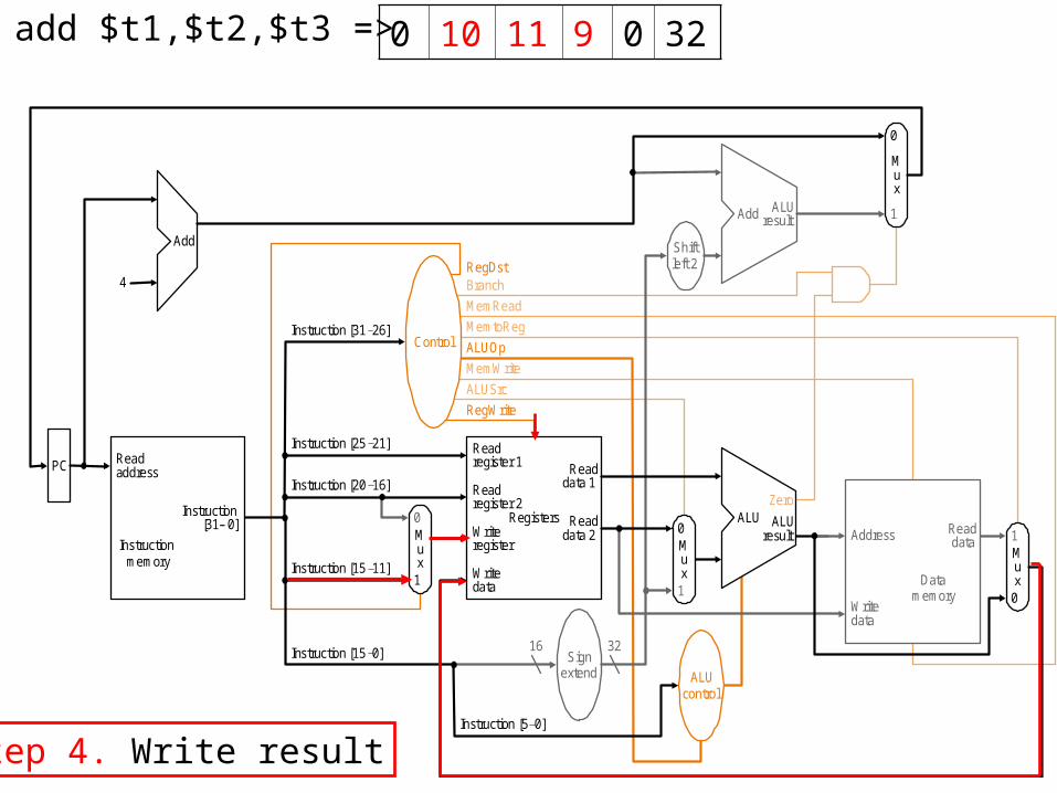
add $t1,$t2,$t3 => add $9, $10, $11 =>
Step 1. Instruction fetch
0 10 11 9 0 32

PC
Instructionmemory
Readaddress
Instruction[31– 0]
Instruction [20– 16]
Instruction [25– 21]
Add
Instruction [5– 0]
MemtoReg
ALUOp
MemWrite
RegWrite
MemRead
BranchRegDst
ALUSrc
Instruction [31– 26]
4
16 32Instruction [15– 0]
0
0Mux
0
1
Control
Add ALUresult
Mux
0
1
RegistersWriteregister
Writedata
Readdata 1
Readdata 2
Readregister 1
Readregister 2
Signextend
Shiftleft 2
Mux
1
ALUresult
Zero
Datamemory
Writedata
Readdata
Mux
1
Instruction [15– 11]
ALUcontrol
ALUAddress
add $t1,$t2,$t3 =>
Step 2. Read source registers
0 10 11 9 0 32

PC
Instructionmemory
Readaddress
Instruction[31– 0]
Instruction [20 16]
Instruction [25 21]
Add
Instruction [5 0]
MemtoReg
ALUOp
MemWrite
RegWrite
MemRead
BranchRegDst
ALUSrc
Instruction [31 26]
4
16 32Instruction [15 0]
0
0Mux
0
1
ALUcontrol
Control
Add ALUresult
Mux
0
1
RegistersWriteregister
Writedata
Readdata 1
Readdata 2
Readregister 1
Readregister 2
Signextend
Mux
1
ALUresult
Zero
Datamemory
ReaddataAddress
Writedata
Mux
1
Instruction [15 11]
ALU
Shiftleft 2
add $t1,$t2,$t3 =>
Step 3. Instruction execution
0 10 11 9 0 32
PC
Instructionmemory
Readaddress
Instruction[31– 0]
Instruction [20 16]
Instruction [25 21]
Add
Instruction [5 0]
MemtoReg
ALUOp
MemWrite
RegWrite
MemRead
BranchRegDst
ALUSrc
Instruction [31 26]
4
16 32Instruction [15 0]
0
0Mux
0
1
ALUcontrol
Control
Shiftleft 2
Add ALUresult
Mux
0
1
RegistersWriteregister
Writedata
Readdata 1
Readdata 2
Readregister 1
Readregister 2
Signextend
Mux
1
ALUresult
Zero
Datamemory
Writedata
Readdata
Mux
1
Instruction [15 11]
ALUAddress
add $t1,$t2,$t3 =>
Step 4. Write result
0 10 11 9 0 32

PC
Instructionmemory
Readaddress
Instruction[31– 0]
Instruction [15– 11]
Instruction [20– 16]
Instruction [25– 21]
Add
Instruction [5– 0]
MemtoReg
ALUOp
MemWrite
RegWrite
MemRead
BranchRegDst
ALUSrc
Instruction [31– 26]
4
16 32Instruction [15– 0]
0
0Mux
0
1
ALUcontrol
Control
Shiftleft 2
Add ALUresult
Mux
0
1
RegistersWriteregister
Writedata
Readdata 1
Readdata 2
Readregister 1
Readregister 2
Signextend
Mux
1
ALUresult
Zero
Datamemory
Writedata
Readdata
Mux
1ALU
Address
lw $t1, 0($t2) 36 9 10 0

How to combine the datapaths ? We have shown datapaths for
Instruction fetch R-type instructions Load/store branch
How to assemble the datapaths? How to handle control lines?

PC
Instructionmemory
Readaddress
Instruction[31– 0]
Instruction [20 16]
Instruction [25 21]
Add
Instruction [5 0]
MemtoReg
ALUOp
MemWrite
RegWrite
MemRead
BranchRegDst
ALUSrc
Instruction [31 26]
4
16 32Instruction [15 0]
0
0Mux
0
1
Control
Add ALUresult
Mux
0
1
RegistersWriteregister
Writedata
Readdata 1
Readdata 2
Readregister 1
Readregister 2
Signextend
Mux
1
ALUresult
Zero
PCSrc
Datamemory
Writedata
Readdata
Mux
1
Instruction [15 11]
ALUcontrol
Shiftleft 2
ALUAddress
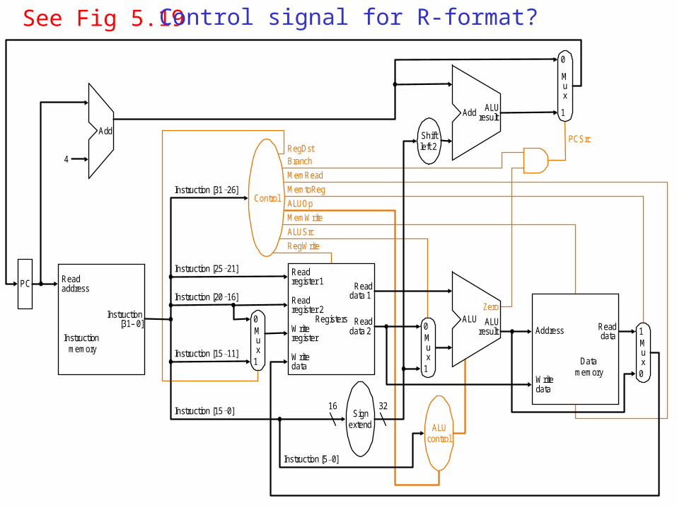
Simple datapath and control. See Fig 5.19 (p.360)

How to generate control?
Truth table look-up
Control signal
6 bits 6 bits
10 bits

Hierarchy of control unitsInstructions (binary representation)
Main control unit
ALUop(2 bits)
Other control signals(6 1-bit)
ALU control unit
ALU control signals(3 bits)

Why multiple levels of control?
Purpose: Reduce the size of main control unit ? Potentially increase the speed of the control
unit ALUop(2 bits) :指令分類
define 3 classes of instructions R-type Load/store Branch

Design main control unit
Instructions (binary representation)
Main control unit
ALUop(2 bits)
ALU control unit
ALU control signals(3 bits)
Other control signals(6 1-bit)
Opcode[31-26]

Main control unit Observe instruction set
PC
Instructionmemory
Readaddress
Instruction[31– 0]
Instruction [20 16]
Instruction [25 21]
Add
Instruction [5 0]
MemtoReg
ALUOp
MemWrite
RegWrite
MemRead
BranchRegDst
ALUSrc
Instruction [31 26]
4
16 32Instruction [15 0]
0
0Mux
0
1
Control
Add ALUresult
Mux
0
1
RegistersWriteregister
Writedata
Readdata 1
Readdata 2
Readregister 1
Readregister 2
Signextend
Mux
1
ALUresult
Zero
PCSrc
Datamemory
Writedata
Readdata
Mux
1
Instruction [15 11]
ALUcontrol
Shiftleft 2
ALUAddress
See Fig 5.19 Control signal for R-format?

10

Create truth table for main control unit

100123456789
101112131415161718192021222324252627282930313233343536373839404142434445464748495051525354555657585960616263
100123456789
101112131415161718192021222324252627282930313233343536373839404142434445464748495051525354555657585960616263
100123456789
101112131415161718192021222324252627282930313233343536373839404142434445464748495051525354555657585960616263
0123456789
10111213141516171819202122232425262728293031
0123456789
10111213141516171819202122232425262728293031
0123456789
10111213141516171819202122232425262728293031
16000102030405060708090a0b0c0d0e0 f101112131415161718191a1b1c1d1e1 f202122232425262728292a2b2c2d2e2 f303132333435363738393a3b3c3d3e3 f
op(31:26)
jjalbeqbneblezbgtzaddiaddiusltisltiuandiorixoriluiz = 0z = 1z = 2z = 3
lblhlwllwlbulhulwr
sbshswlsw
swr
lwc0lwc1lwc2lwc3
swc0swc1swc2swc3
rs(25:21)mfcz
cfcz
mtcz
ctcz
copzcopz
(16:16)bcztbczt
tlbrtlbwi
tlbwrtlbp
rte
rt (20:16)
bltzbgez
bltzalbgezal
cvt.s.fcvt.d.f
cvt.w.f
c.f.fc.un.fc.eq.fc.ueq.fc.olt.fc.ult.fc.ole.fc.ule.fc.st.fc.ngle.fc.seq.fc.ngl.fc.lt.fc.nge.fc.le.fc.ngt.f
funct(5:0)add.fsub.fmul.fdiv.f
abs.fmov.fneg.f
funct(5:0)sll
srlsra
srlvsravjrjalr
syscallbreak
mfhimthimflomtlo
multmultudivdivu
addaddusubsubuandorxornor
sltsltu
if z = l,f = d
if z = l,f = s
if z = 0
01
funct(4:0)

Design ALU control unitInstructions (binary representation)
Main control unit
ALUop(2 bits)
ALU control unit
ALU control signals(3 bits)
Other control signals(6 1-bit)
Opcode[31-26]
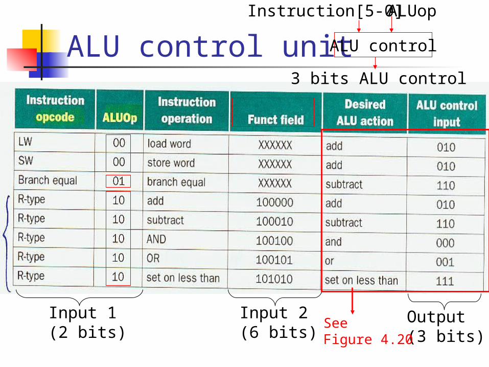
ALU control unit
Input 1(2 bits)
Input 2(6 bits)
Output(3 bits)
ALU control
ALUopInstruction[5-0]
3 bits ALU control
SeeFigure 4.20

ALU control signal
0
3
Result
Operation
a
1
CarryIn
CarryOut
0
1
Binvert
b 2
Less
0
3
Result
Operation
a
1
CarryIn
0
1
Binvert
b 2
Less
Set
Overflowdetection
Overflow
a.
b.
(2 bits)(1 bit)
+
ALU control line function0 00 and0 01 or0 10 add1 10 sub1 11 slt

Instruction set formats instruction set
決定 ALU動作

creating truth table
28

PC
Instructionmemory
Readaddress
Instruction[31– 0]
Instruction [20 16]
Instruction [25 21]
Add
Instruction [5 0]
MemtoReg
ALUOp
MemWrite
RegWrite
MemRead
BranchRegDst
ALUSrc
Instruction [31 26]
4
16 32Instruction [15 0]
0
0Mux
0
1
Control
Add ALUresult
Mux
0
1
RegistersWriteregister
Writedata
Readdata 1
Readdata 2
Readregister 1
Readregister 2
Signextend
Mux
1
ALUresult
Zero
PCSrc
Datamemory
Writedata
Readdata
Mux
1
Instruction [15 11]
ALUcontrol
Shiftleft 2
ALUAddress
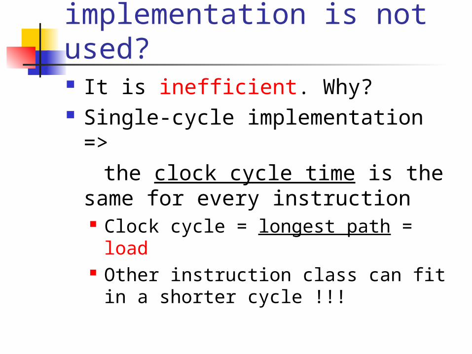
Why a single-cycle implementation is not used? It is inefficient. Why? Single-cycle implementation => the clock cycle time is the same
for every instruction Clock cycle = longest path = load Other instruction class can fit in a
shorter cycle !!!

Performance evaluation for single-cycle implementation Assume the operation time
Memory units: 2 ns ALU: 2ns Register file: 1 ns
Calculate the necessary time for each instruction class

Memory units: 2 nsALU: 2nsRegister file: 1 ns

How to improve single-cycle datapath? A variable-speed clock for each
instruction class Difficult to implement
Multi-cycle implementation