shenzhen vatronix technology co.,ltd. character...
TRANSCRIPT
Shenzhen Vatronix Technology CO.,LTD. Character LCM User Manual
Page 1 / 13
How to control a SPLC780D-based Character LCM:TC1602A 1.Outline Dimension In case of further question, please contact your Vatronix contact windows. 2.Interface Description
Pin No. Symbol Level Description
1 VSS 0V Ground 2 VDD 5.0V Power supply for Logic 3 VO (Variable) Driving voltage for LCD 4 RS H/L H:Data L :Instruction 5 RW H/L H:Read L:Write 6 E H/L Enable signal
7~14 DB0~DB7 H/L Data bus. DB7 is used for Busy Flag . 15 A(LED+) +5V Anode of LED Backlight 16 K(LED-) 0V Cathode of LED Backlight
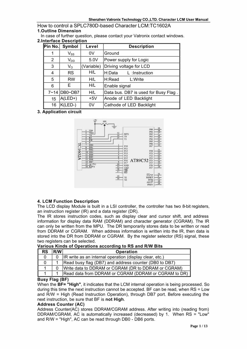
3. Application circuit
4. LCM Function Description The LCD display Module is built in a LSI controller, the controller has two 8-bit registers, an instruction register (IR) and a data register (DR). The IR stores instruction codes, such as display clear and cursor shift, and address information for display data RAM (DDRAM) and character generator (CGRAM). The IR can only be written from the MPU. The DR temporarily stores data to be written or read from DDRAM or CGRAM. When address information is written into the IR, then data is stored into the DR from DDRAM or CGRAM. By the register selector (RS) signal, these two registers can be selected. Various Kinds of Operations according to RS and R/W Bits
RS R/W Operation 0 0 IR write as an internal operation (display clear, etc.) 0 1 Read busy flag (DB7) and address counter (DB0 to DB7) 1 0 Write data to DDRAM or CGRAM (DR to DDRAM or CGRAM) 1 1 Read data from DDRAM or CGRAM (DDRAM or CGRAM to DR)
Busy Flag (BF) When the BF= "High", it indicates that the LCM internal operation is being processed. So during this time the next instruction cannot be accepted. BF can be read, when RS = Low and R/W = High (Read Instruction Operation), through DB7 port. Before executing the next instruction, be sure that BF is not High. Address Counter (AC) Address Counter(AC) stores DDRAM/CGRAM address. After writing into (reading from) DDRAM/CGRAM, AC is automatically increased (decreased) by 1. When RS = "Low" and R/W = "High", AC can be read through DB0 - DB6 ports.

Shenzhen Vatronix Technology CO.,LTD. Character LCM User Manual
Page 2 / 13
Display Data RAM (DDRAM) This DDRAM is used to store the display data represented in 8-bit character codes. Below figure is the relationships between DDRAM addresses and positions on the liquid crystal display.
TC1602A DDRAM Address (16CharsX2Lines, In HEX) Character Generator ROM (CGROM) The CGROM generate 5×8 dot or 5×10 dot character patterns from 8-bit character codes. See “Standard Character pattern”. Character Generator RAM (CGRAM) In CGRAM, the user can rewrite character by program. Relationship between Character Code (DDRAM) and Character Pattern (CGRAM) shown as flow.
“ X”: don’t care
16 Chars X 2 Lines Display CharNo 1 2 3 4 5 6 7 8 9 10 11 12 13 14 15 16 1st Line 00 01 02 03 04 05 06 07 08 09 0A 0B 0C 0D 0E 0F 2nd Line 40 41 42 43 44 45 46 47 48 49 4A 4B 4C 4D 4E 4F
Char Code(DDRAM data) CGRAM address CGRAM data D7 D6 D5 D4 D3 D2 D1 D0 A5 A4 A3 A2 A1 A0 P7 P6 P5 P4 P3 P2 P1 P0
Pattern number
0 0 0 0 X 0 0 0 0 0 0 0 0 0 X X X 0 1 1 1 0 0 0 1 1 0 0 0 1 0 1 0 1 0 0 0 1 0 1 1 1 1 1 1 1 1 0 0 1 0 0 0 1 1 0 1 1 0 0 0 1 1 1 0 1 0 0 0 1
.
.
.
.
.
.
.
.
.
.
.
.
.
. 1 1 1
.
.
.
.
.
.
. 0 0 0 0 0
Pattern 1
.
.
.
.
.
.
.
.
.
.
.
.
.
.
. 0 0 0 0 X 1 1 1 1 1 1 0 0 0 X X X 1 0 0 0 1
0 0 1 1 0 0 0 1 0 1 0 1 0 0 0 1 0 1 1 1 1 1 1 1 1 0 0 1 0 0 0 1 1 0 1 1 0 0 0 1 1 1 0 1 0 0 0 1
.
.
.
.
.
.
.
.
.
.
.
.
.
. 1 1 1
.
.
.
.
.
.
. 0 0 0 0 0
Pattern 8

Shenzhen Vatronix Technology CO.,LTD. Character LCM User Manual
Page 3 / 13
5. User instruction Definitions 5.1 Instruction table
5.2 Instruction Description 1)Clear Display
RS RW DB7 DB6 DB5 DB4 DB3 DB2 DB1 DB0
0 0 0 0 0 0 0 0 0 1 Clear all the display data by writing "20H" (space code) to all DDRAM address, and set DDRAM address to "00H" into AC (address counter). Return cursor to the original status. Namely, bring the cursor to the left edge on first line of the display. Make entry mode increment (I/D = "1"). 2) Return Home
RS RW DB7 DB6 DB5 DB4 DB3 DB2 DB1 DB0
0 0 0 0 0 0 0 0 1 - Return Home is cursor return home instruction. Set DDRAM address to "00H" into the address counter. Return cursor to its original site and return display to its original status, if shifted. Contents of DDRAM do not change. 3) Entry Mode Set
RS RW DB7 DB6 DB5 DB4 DB3 DB2 DB1 DB0 0 0 0 0 0 0 0 1 I/D SH
Set the moving direction of cursor and display. I/D: Increment / decrement of DDRAM address (cursor or blink)
When I/D = "High", cursor/blink moves to right and DDRAM address is increased by 1. When I/D = "Low", cursor/blink moves to left and DDRAM address is decreased by 1.
* CGRAM operates the same as DDRAM, when read from or write to CGRAM. SH: Shift of entire display When DDRAM read (CGRAM read / write) operation or SH = "Low", shift of entire display

Shenzhen Vatronix Technology CO.,LTD. Character LCM User Manual
Page 4 / 13
is not performed. If SH = "High" and DDRAM write operation, shift of entire display is performed according to I/D value:
I/D ="1" : shift left, I/D = "0" : shift right.
4) Display ON/OFF Control RS RW DB7 DB6 DB5 DB4 DB3 DB2 DB1 DB0 0 0 0 0 0 0 1 D C B
Control display / cursor / blink ON / OFF 1 bit register. D: Display ON / OFF control bit
When D = "High", entire display is turned on. When D = "Low", display is turned off, but display data is remained in DDRAM.
C: Cursor ON / OFF control bit When C = "High", cursor is turned on. When C = "Low", Cursor is disappeared in current display, but I/D register remains its data.
B: Cursor Blink ON / OFF control bit When B = "High", cursor blink is on, that performs alternate between all the high data and display character at the cursor position. When B = "Low", blink is off.
5) Cursor or Display Shift RS RW DB7 DB6 DB5 DB4 DB3 DB2 DB1 DB0 0 0 0 0 0 1 S/C R/L - -
Shifting of right/left cursor position or display Without Writing or reading of display data, shift right/left cursor position or display. This instruction is used to correct or search display data. (refer to Table 4) During 2-line mode display, cursor moves to the 2nd line after 40th digit of 1st line. Note that display shift is performed simultaneously in all the line. When displayed data is shifted repeatedly, each line shifted individually. When display shift is performed, the contents of address counter are not changed. S/C R/L Operation
0 0 Shift the cursor to the left, AC is decreased by 1. 0 1 Shift the cursor to the right, AC is increased by 1. 1 0 Shift all the display to the left, cursor moves according to the display. 1 1 Shift all the display to the right, cursor moves according to the display.
6) Function Set RS RW DB7 DB6 DB5 DB4 DB3 DB2 DB1 DB0 0 0 0 0 1 DL N F - -
DL: Interface data length control bit When DL = "High", it means 8-bit bus mode with MPU. When DL = "Low", it means 4-bit bus mode with MPU.
When 4-bit bus mode, it needs to transfer 4-bit data by two times. N: Display line number control bit
When N = "Low", it means 1-line display mode. When N = "High", 2-line display mode is set.
F: Display font type control bit When F = "Low", it means 5 x 8 dots format display mode When F = "High", 5 x11 dots format display mode.
7) Set CGRAM Address RS RW DB7 DB6 DB5 DB4 DB3 DB2 DB1 DB0 0 0 0 1 AC5 AC4 AC3 AC2 AC1 AC0
Set CGRAM address to AC. This instruction makes CGRAM data available from MPU. 8) Set DDRAM Address
RS RW DB7 DB6 DB5 DB4 DB3 DB2 DB1 DB0 0 0 1 AC6 AC5 AC4 AC3 AC2 AC1 AC0
Set DDRAM address to AC. This instruction makes DDRAM data available from MPU. When 1-line display mode (N = 0), DDRAM address is from "00H" to "4FH". In 2-line display mode (N = 1), DDRAM address is the 1st line is from "00H" to "27H", and DDRAM address in the 2nd line is from "40H" to "67H".

Shenzhen Vatronix Technology CO.,LTD. Character LCM User Manual
Page 5 / 13
9) Read Busy Flag & Address RS RW DB7 DB6 DB5 DB4 DB3 DB2 DB1 DB0 0 1 BF AC6 AC5 AC4 AC3 AC2 AC1 AC0
This instruction shows whether LCM is in internal operation or not. If the resultant BF is High, it means the internal operation is in progress and you have to wait until BF to be Low, and then the next instruction can be performed. In this instruction you can read also the value of address counter. 10) Write data to RAM
RS RW DB7 DB6 DB5 DB4 DB3 DB2 DB1 DB0 1 0 D7 D6 D5 D4 D3 D2 D1 D0
Write binary 8-bit data to DDRAM/CGRAM. The selection of RAM from DDRAM, CGRAM, is set by the previous address set instruction: DDRAM address set, CGRAM address set. RAM set instruction can also determine the AC direction to RAM. After write operation, the address is automatically increased/decreased by 1, according to the entry mode. 11) Read data from RAM
RS RW DB7 DB6 DB5 DB4 DB3 DB2 DB1 DB0 1 1 D7 D6 D5 D4 D3 D2 D1 D0
Read binary 8-bit data from DDRAM/CGRAM. The selection of RAM is set by the previous address set instruction. If address set instruction of RAM is not performed before this instruction, the data that read first is invalid, because the direction of AC is not determined. If you read RAM data several times without RAM address set instruction before read operation, you can get correct RAM data from the second, but the first data would be incorrect, because there is no time margin to transfer RAM data. In case of DDRAM read operation, cursor shift instruction plays the same role as DDRAM address set instruction : it also transfer RAM data to output data register. After read operation address counter is automatically increased/decreased by 1 according to the entry mode. After CGRAM read operation, display shift may not be executed correctly. * In case of RAM write operation, after this AC is increased/decreased by 1 like read operation. In this time, AC indicates the next address position, but you can read only the previous data by read instruction.

Shenzhen Vatronix Technology CO.,LTD. Character LCM User Manual
Page 6 / 13
6. Timing Characteristics

Shenzhen Vatronix Technology CO.,LTD. Character LCM User Manual
Page 7 / 13
7.Initializing flow chart l 8-bit interface mode

Shenzhen Vatronix Technology CO.,LTD. Character LCM User Manual
Page 8 / 13
l 4-bit interface mode
Shenzhen Vatronix Technology CO.,LTD. Character LCM User Manual
Page 9 / 13
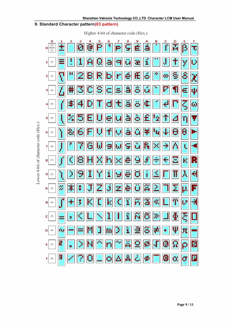
9. Standard Character pattern(03 pattern)

Shenzhen Vatronix Technology CO.,LTD. Character LCM User Manual
Page 10 / 13
10.Demo program RS EQU P3.3 RW EQU P3.4 E EQU P3.5 COM EQU 20H DAT EQU 21H ORG 0000H MOV SP,#60H LJMP DISP ORG 0040H DISP: LCALL DELAY MOV COM,#38H ; Function Set ACALL WRI ;Write Instruction LCALL DELAY ;Delay MOV COM,#0EH ; Display ON/OFF ACALL WRI ; Write Instruction LCALL DELAY ; Delay MOV COM,#01H ; Clear Display ACALL WRI LCALL DELAY MOV COM,#06H ; Entry Mode Set ACALL WRI MOV COM,#40H ;Set CGRAM Address ACALL WRI LCALL CGRAM ; Character Generate subroutine AGAIN: MOV DPTR,#TAB1 LCALL DispSTR LCALL DELAY1 JB P3.2,$
MOV R3,#05 MOV A,#00H ;Display CGRAM CODE:00H~04H NEXT: LCALL DISP1 LCALL DELAY1 JB P3.2,$ ;Step display MOV COM,#0CH ; Display ON/OFF ACALL WRI MOV COM,#01H ; Clear Display ACALL WRI INC A DJNZ R3,NEXT ;LOOP until CGRAM CODE: 04H MOV A,#41H ; Display “ A” LCALL DISP1 LCALL DELAY1 JB P3.2,$ MOV A,#50H ; Display “P” LCALL DISP1 LCALL DELAY1 JB P3.2,$ MOV A,#0C2H ; Display “ ” LCALL DISP1 LCALL DELAY1 JB P3.2,$ MOV A,#0F7H ; Display “ ” LCALL DISP1 LCALL DELAY1 JB P3.2,$

Shenzhen Vatronix Technology CO.,LTD. Character LCM User Manual
Page 11 / 13
MOV R2,A MOV COM,#0CH ACALL WRI MOV COM,#01H ACALL WRI LJMP AGAIN ;********************************************************** DISP1: MOV COM,#0EH ACALL WRI MOV R4,#16 ;LOOP 16 times MOV COM,#80H ;Set 1st Line DDRAM Address to 00H(1st CHAR.) ACALL WRI DEMO1:MOV DAT,A
LCALL WRD ;Display data LCALL DELAY DJNZ R4,DEMO1 ;LOOP 16 times
MOV COM,#0C0H ;Set 2nd Line DDRAM Address to C0H(1st CHAR.) ACALL WRI MOV R4,#16 DEMO2:MOV DAT,A LCALL WRD
LCALL DELAY1 DJNZ R4,DEMO2 RET
;**************************************** Write Instruction subroutine WRI: PUSH ACC CLR RS SETB RW WRI1: MOV P1,#0FFH SETB E MOV A,P1 CLR E JB ACC.7,WRI1 CLR RW MOV P1,COM SETB E CLR E POP ACC RET ;**************************************** Write DATA subroutine WRD: PUSH ACC CLR RS SETB RW WRD1: MOV P1,#0FFH SETB E MOV A,P1 CLR E JB ACC.7,WRD1 SETB RS CLR RW MOV P1,DAT SETB E CLR E POP ACC RET ;**************************************** Display strings subroutine DispSTR:
MOV R2,#16 MOV COM,#080H ACALL WRI DSTR1: MOV A,#00H MOVC A,@A+DPTR MOV DAT,A CALL WRD INC DPTR DJNZ R2,DSTR1

Shenzhen Vatronix Technology CO.,LTD. Character LCM User Manual
Page 12 / 13
MOV R2,#16 MOV COM,#0C0H ACALL WRI DSTR2: MOV A,#00H MOVC A,@A+DPTR MOV DAT,A CALL WRD INC DPTR DJNZ R2,DSTR2 RET ;************************************ Delay subroutine DELAY: MOV R5,#060H DELAY4: MOV R6,#000H LOOP2: DJNZ R6,LOOP2 DJNZ R5,DELAY4 RET ;************************************ Delay subroutine DELAY1: MOV R5,#0FFH DL1: MOV R6,#0FFH DL2: DJNZ R6,DL2
DJNZ R5,DL1 RET ;************************************ Character Generate subroutine CGRAM:
MOV R2,#40 MOV DPTR,#TAB
CGRAM1: MOV A,#00H MOVC A,@A+DPTR MOV DAT,A
LCALL WRD INC DPTR DJNZ R2,CGRAM1 RET ;************************************ CGRAM CODE TAB: DB 015H,00AH,015H,00AH,015H,00AH,015H,00AH DB 0FFH,0FFH,0FFH,0FFH,0FFH,0FFH,0FFH,0FFH DB 000H,000H,000H,000H,000H,000H,000H,000H DB 0FFH,000H,0FFH,000H,0FFH,000H,0FFH,000H DB 015H,015H,015H,015H,015H,015H,015H,015H TAB1: DB 'Vatronix TC1602A' DB 'Size:122X44X13.5' END ;This program debugged through Keil C.

Shenzhen Vatronix Technology CO.,LTD. Character LCM User Manual
Page 13 / 13
Vatronix Character LCM DDRAM Address(In HEX): 16 Chars X 1 Line (TC1601 serial)
CharNo 1 2 3 4 5 6 7 8 9 10 11 12 13 14 15 16 1st Line 00 01 02 03 04 05 06 07 40 41 42 43 44 45 46 47
16 Chars X 2 Lines (TC1602 serial) CharNo 1 2 3 4 5 6 7 8 9 10 11 12 13 14 15 16 1st Line 00 01 02 03 04 05 06 07 08 09 0A 0B 0C 0D 0E 0F 2nd Line 40 41 42 43 44 45 46 47 48 49 4A 4B 4C 4D 4E 4F
20 Chars X 2 Line s (TC2002 serial) CharNo 1 2 3 4 5 6 … … 13 14 15 16 17 18 19 20 1st Line 00 01 02 03 04 05 … … 0C 0D 0E 0F 10 11 12 13 2nd Line 40 41 42 43 44 45 … … 4C 4D 4E 4F 50 51 52 53
40 Chars X 2 Lines (TC4002 serial) CharNo 1 2 3 4 5 6 … … 33 34 35 36 37 38 39 40 1st Line 00 01 02 03 04 05 … … 20 21 22 23 24 25 26 27 2nd Line 40 41 42 43 44 45 … … 60 61 62 63 64 65 66 67
16 Chars X 4 Lines (TC1604 serial) CharNo 1 2 3 4 5 6 … … 9 10 11 12 13 14 15 16 1st Line 00 01 02 03 04 05 … … 08 09 0A 0B 0C 0D 0E 0F 2nd Line 40 41 42 43 44 45 … … 48 49 4B 4B 4C 4D 4E 4F 3rd Line 10 11 12 13 14 15 … … 18 19 1A 1B 1C 1D 1E 1F 4th Line 50 51 52 53 54 55 … … 58 59 5A 5B 5C 5D 5E 5F
20 Chars X 4 Lines (TC2004 serial) CharNo 1 2 3 4 5 6 … … 13 14 15 16 17 18 19 20 1st Line 00 01 02 03 04 05 … … 0C 0D 0E 0F 10 11 12 13 2nd Line 40 41 42 43 44 45 … … 4C 4D 4E 4F 50 51 52 53 3rd Line 14 15 16 17 18 19 … … 20 21 22 23 24 25 26 27 4th Line 54 55 56 57 58 59 … … 60 61 62 63 64 65 66 67
40 Chars X 4 Lines (TC4004 serial) Char No. 1 2 3 4 5 … … 33 34 35 36 37 38 39 40
1st Line 00 01 02 03 04 … … 20 21 22 23 24 25 26 27 1ST Chip 2nd Line 40 41 42 43 44 … … 60 61 62 63 64 65 66 67
1st Line 00 01 02 03 04 … … 20 21 22 23 24 25 26 27 2ND Chip 2nd Line 40 41 42 43 44 … … 60 61 62 63 64 65 66 67