shankersinh vaghela bapu institute of technology basic electronics shankersinh vaghela bapu...
TRANSCRIPT
131101: Basic Electronics Shankersinh Vaghela Bapu Institute of Technology
1
Shankersinh Vaghela Bapu Institute of Technology
B.E. Semester III (EC)
131101: Basic Electronics INDEX
Sr. No.
Title Page Date Sign Grade
1 [A] To Study the V-I characteristic of PN junction diode. [B] To Study the V-I characteristic of Zener diode.
2 To observe the output waveform of half wave and full wave rectifier.
3 To study the operation of the positive and negative clipper with clipping level at zero volt.
4 To study the operation Clamper circuits
5
[A] To plot the input and output characteristics of PNP and NPN Transistor in CE configuration. [B] To find the h-parameters for the same.
6 [A] To plot the input and output characteristics of PNP and NPN Transistor in CB configuration. [B] To find the h-parameters for the same.
7 To plot the input and output characteristics of PNP and NPN Transistor in CC configuration. [B] To find the h-parameters for the same.
8 To study the operation of class A power amplifier.
9 To study the operation of class B power amplifier.
10 To plot drain and transfer characteristics of FET.

131101: Basic Electronics Shankersinh Vaghela Bapu Institute of Technology
2
Roll No.: Date: Exp. No.: Title : Characteristics of diode. _____________________________________________________________________ AIM: To plot the characteristics of diode under forward bias and reverse bias Condition EQUIPMENTS: [1]. Experiment board [2]. Ammeter - 2 (0-30 mA) and (0-100 µA) [3]. Voltmeter - 2 (0-1 V) and (0-10 V) [4]. Power supply - 1 (0-10 V) THEORY: A p-n junction diode is formed by joining a p-type and n-type semiconductor material. It is a two terminal, uni-junction, uni-directional device. If the positive terminal of the supply is connected to anode (p-region) and negative terminal is connected to cathode (n-region), the diode is said to be forward biased. If the connections are reversed, the diode is said to be reverse biased. Unbiased diode: When the diode is unbiased, diffusion of carriers take place because the concentration of hole is more in p-region and less in n-region and concentration of electron is more in n-region and less in p-region. Hence, holes from p-region diffuse to n-region and electrons from n-region diffuse to p-region. As soon As these charge carriers cross the junction, they recombine with opposite polarity charges. These recombined carriers neutral in charge and they oppose the further movement of charge carriers from one region to another. The region near the junction, occupied by the recombined charges, is known as depletion region or space charge region or transition region. The difference of potential across this region i.e. barrier potential is 0.6 V to 0.7 V for Silicon diode and 0.2 V to 0.3 V for Germanium diode. Forward biased diode: When the diode is forward biased and the applied bias is less than barrier potential, no current flows. As the applied potential increases, the charge carriers gain sufficient energy to cross barrier potential and enter the other region. The holes enter the n-region and the electrons enter the p-region, crossing the p-n junction. This crossing of charge carriers results in a flow of current. This is called drift current. Reverse biased diode: When the diode is reverse biased the majority charge carriers are attracted towards the terminals of applied potential away from the p-n junction. It results in widening of the depletion region. Under this situation, no current flows across the p-n junction. But, there will be a very small current across the p-n junction due to the thermally generated minority carriers, called reverse saturation current. It is independent of applied potential and increases

131101: Basic Electronics Shankersinh Vaghela Bapu Institute of Technology
3
with temperature. When the applied reverse voltage increased beyond limit, it results in break down. During break down, the diode current increases tremendously for a particular voltage. When a p-n junction diode is heavily doped, it is known as Zener diode. When the Zener diode is forward bias, it exhibits the same characteristics as p-n junction diode. In reverse biased condition, when reverse voltage increases beyond breakdown voltage, current through diode rises sharply. Beyond breakdown very small rise in voltage results in large current through the diode. Due to applied reverse potential, an electric field exists near the junction. This field exerts a strong force on the bound charges, which breaks the covalent bonds and releases free charge carrier. These newly generated electron-hole pairs result in sudden increase of reverse current. As the level of doping increases, the breakdown voltage reduces. Such diode exhibits negative coefficient of temperature. Zener diode, connected in reverse biased condition, is used as a voltage regulator. Once the reverse voltage crosses breakdown voltage, voltage across the zener diode remains constant even if current through the diode increases sharply . PROCEDURE: [1] Connect the circuit as per the circuit diagram (1). [2] Increase the power supply voltage such that the voltage across the diode changes by 0.1V
till the power supply meter shows 20V. [3] Note down the corresponding ammeter readings. [4] Plot the graph: I against V. [5] Find the dynamic resistance from the slope of the graph: r = ∇ V / ∇ I at I = 10mA. [6] Connect the circuit as per the circuit diagram (2). [7] Increase the power supply voltage such that the voltage across the diode changes by 1V
till the power supply meter shows 20V. [8] Note down the corresponding ammeter readings. [9] Plot the graph: I against V. [10]Find the dynamic resistance from the slope of the graph: r = ∇ V / ∇ I at V = 10V. [11]Repeat steps 1 to 10 for Zener diode.

131101: Basic Electronics Shankersinh Vaghela Bapu Institute of Technology
4
OBSERVATION TABLE: JUNCTION DIODE Forward bias Reverse bias
Sr.No. Diode voltage, V
Diode Current, I
Sr.No. Diode voltage, V
Diode Current, I
RESULTS:
Dynamic resistance R=∇ V/ ∇ I
Junction Diode
Forward bias Reverse bias
CONCLUSION:

131101: Basic Electronics Shankersinh Vaghela Bapu Institute of Technology
5
CIRCUIT DIAGRAM :
0-30 V
A
0-100uA
0-10 V
+
+ +
10KΩ
FIGURE :1
FIGURE :2
0-30 V
1KΩ A
V
0-30 mA
0-1 V
+
+ +
V
OR
OR

131101: Basic Electronics Shankersinh Vaghela Bapu Institute of Technology
6
Answer the following questions: [1] What is the difference between the drift current and diffusion current? [2] Which factor is responsible for generation of reverse saturation current and why it is
independent of applied potential? [3] Define cut in voltage. What is the value of cut in voltage for germanium diode and silicon
diode? [4] Explain how the zener diode can be used as voltage regulator. Also show the region in
the characteristics where it behaves so. [5] Draw the Ideal Characteristics of PN junction diode.

131101: Basic Electronics Shankersinh Vaghela Bapu Institute of Technology
7
Roll No.: Date: Exp. No.: Title : Half wave and Full wave Rectifier ______________________________________________________________________________ AIM : [1] To plot the output waveforms of following rectifiers with and without capacitor filter.
(i). Half wave rectifier (ii). Full wave center taped rectifier (iii).Bridge rectifier
[2] To determine its ripple factor. EQUIPMENTS: [1]. Experiment board [2]. C.R.O. [3]. Multimeter THEORY: The process of converting an alternating voltage/current to a unidirectional voltage/current is called rectification. A diode offers very low resistance when forward biased and very high resistance when reverse biased. Hence, it can be used as rectifier. The rectified output is a pulsating unidirectional voltage/current. A filter is necessary after rectifier to convert pulsating waveform to dc. Half wave rectifier: During positive half cycle, the diode is forward biased. Hence, current flows through load resistor. During negative half cycle, the diode is reverse biased and is equivalent to open circuit. Therefore current through load is zero. Thus, the diode conducts only for one half cycles and results in half wave rectified output. Half wave rectifier is simple and low cost circuit but it has very high ripple, lower efficiency. Full wave rectifier: The full wave rectifier consists of a center-tap transformer, which results in equal voltages above and below the center-tap. During the positive half cycle, positive voltage appears at the anode of D1 while negative voltage at the anode of D2. So diode D1 is forward biased and it results in current through load. During negative half cycle, the positive voltage appears at the anode of D2 and hence it is forward biased resulting in current through load. At the same instant a negative voltage appears at the anode of D1, thus reverse biasing it and hence D1 does not conduct. The current through the load during both half cycles is in the same direction hence it is sum of individual currents. The individual currents and voltages are combined in the load and therefore their average values are double that obtained in a half wave rectifier. In full wave rectifier, ripple is reduced, efficiency is improved. And as equal current flows through secondary during both the half cycle, core does not saturate. The demerits of full wave rectifier are : output voltage is half the secondary voltage and diodes with high PIV ratings are required.

131101: Basic Electronics Shankersinh Vaghela Bapu Institute of Technology
8
Bridge rectifier: This circuit does not required center-tap transformer. During the positive half cycle, diodes D1 and D2 are forward biased and D3 and D4 are reverse biased. Thus, current flows in the circuit due to D1 and D2. During the positive half cycle, diodes D1 and D2 are forward biased and D3 and D4 are reverse biased. Thus, current flows in the circuit due to D1 and D2. During the negative half cycle, diodes D3 and D4 are forward biased and D1 and D2 are reverse biased which results in a current in the same direction. Thus the current flows for the whole cycle across the load in one direction resulting in full wave rectification. Since bridge rectifier does not required center-tapped transformer, its cost, weight and size are lesser compared to a full wave rectifier. Diode with lesser PIV can be used in bridge rectifier compared to full wave rectifier. FORMULA:
For half wave rectifier
For full wave rectifier (center tapped & bridge )
Vdc = Vm / π
Vdc = 2Vm / π
Vrms = Vm / 2
Vrms = Vm / √2
Vrms' = √ (Vrms2 - Vdc2) (without filter)
Vrms' = Vm' / √ 2 (with filter)
Vrms' = √ (Vrms2 - Vdc2) (without filter) Vrms' = Vm' / √ 2 (with filter)
where, Vm - peak value of the pulsating waveform Vrms - root mean square value of the total output Vrms' - root mean square value of ripple Vm' - peak value of the ripple PROCEDURE : [1] Complete the circuit as per the fig.(1) for half wave rectifier. [2] Connect the CRO across the load. [3] Switch on the supply. [4] Keep the CRO in ground mode and adjust the horizontal line on X-axis. [5] Switch the CRO to DC mode and draw the waveform. Note down its amplitude Vm. [6] Calculate Vdc, Vrms and Vrms' from the formula given in above table. [7] From Vrms' and Vdc, find out ripple factor. [8] Now, connect the capacitor filter at the output of rectifier, draw the resulting waveform
and measure the peak value, Vp. [9] By keeping the CRO in AC mode, observe the ripple output and measure the peak value
Vm'. [10]Calculate Vdc = Vp- Vm'. [11]Calculate Vrms' from the formula given in above table and from Vrms' and Vdc,
Calculate the ripple factor. [12]Complete the circuit as shown in fig.(2) for full wave centre tapped rectifier and repeat
the steps 5 to 11.

131101: Basic Electronics Shankersinh Vaghela Bapu Institute of Technology
9
[13]Complete the circuit as shown in fig.(3) for bridge rectifier and repeat the steps 5 to 11. OBSERVATION TABLE : • WITHOUT FILTER :
Rectifier Type
Vm measured
(Volts) (dc mode)
Vdc Calculated
Volts
Vrms calculated
(Volts)
Vrms' calculated
(Volts)
Ripple factor γ =
Vrms'/Vdc
Half wave rectifier
Full wave (CT) rectifier
Bridge rectifier
• WITH FILTER :
Rectifier Type
Vp measured
(Volts) (dc mode)
V'm Measured
(Volts) (ac mode)
Vdc calculated
(Volts)
V'rms calculated
(Volts)
Ripple factor γ =
V'rms/Vdc
Half wave rectifier
Full wave (CT) rectifier
Bridge rectifier
RESULT :
Ripple factor with out filter
Ripple factor with filter Theoretical Practical Theoretical Practical
Half wave rectifier
=1/(2√3fCRL)
Full wave rectifier
=1/(4√3fCRL)
Bridge rectifier
=1/(4√3fCRL)
C=0.1uF & RL = 10K CONCLUSION :
131101: Basic Electronics Shankersinh Vaghela Bapu Institute of Technology
10
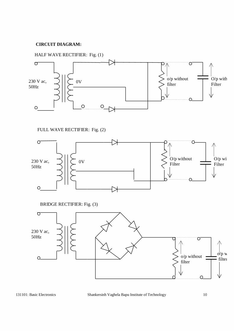
CIRCUIT DIAGRAM: HALF WAVE RECTIFIER: Fig. (1)
230 V ac, 50Hz
o/p without filter
O/p withFilter 0V
O/p withFilter
O/p without Filter
FULL WAVE RECTIFIER: Fig. (2)
230 V ac, 50Hz
0V
o/p with filter
230 V ac, 50Hz
o/p without filter
BRIDGE RECTIFIER: Fig. (3)

131101: Basic Electronics Shankersinh Vaghela Bapu Institute of Technology
11
Title : Half wave and Full wave Rectifier Answer the following questions: Complete the following table: Parameter Half wave
rectifier Full wave
rectifier Bridge
rectifier DC current
DC voltage
RMS current
RMS voltage
Ripple voltage
Efficiency, η
Peak Inverse Voltage
[1] Define peak inverse voltage, ripple factor. [2] Explain how C filter removes ripple. [3] What are the advantages of using bridge rectifier over center tapped full wave rectifier.

131101: Basic Electronics Shankersinh Vaghela Bapu Institute of Technology
12
[4] Select the suitable answer for the following: • The regulation of an excellent rectifier should be (a) infinity (b) zero (c) negative • The ripple frequency of full wave rectified output is (a) 50 Hz (b) 100 Hz (c) 0 Hz • Output voltage in a half wave rectifier consists of (a) dc only (b) ac only (c) ac and dc
both [5]When one of the diode of the bridge rectifier is not working, what will be the output? [6]What changes should be done to reverse the polarity of the output of the rectifier?

131101: Basic Electronics Shankersinh Vaghela Bapu Institute of Technology
13
Roll No.: Date: Exp. No.: Title: Diode Clippers ________________________________________________________________________ AIM: To test the different types of clipping circuits using diodes. EQUIPMENTS:
[1] Circuit board [2] Regulated power supply [3] Audio signal generator [4] C.R.O.
THEORY: The circuit used to limit or clip the extremities of the ac signal is called the limiter or clipper. Limiters can transform a sine wave into a rectangular wave. It can limit either the positive or negative amplitude of an ac voltage. It can also perform other useful wave shaping functions. The unidirectional characteristics of semiconductor diodes permit to serve as limiter. In Figure 1, a sine wave signal of amplitude V in is applied to the input. During the positive half cycle of the input signal, diode D is reversed biased and cannot conduct. Hence the output obtained at the output terminals is zero. During the negative half cycle of the input signal, diode D is forward biased and current can flow in the circuit. Hence at the output terminal, the output voltage Vo will be developed which will be having full negative half cycles and clipped positive half cycles. This circuit is known as positive series clipper because the diode is in series with the output terminal and the output is clipped on the positive side. By reversing the polarity of diode negative series clipper can be realized which can give the output voltage Vo with full positive half cycles and clipped negative half cycles. In Figure 2, a sine wave signal of amplitude Vin is applied to the input. During the positive half cycle of the input signal, diode D is reversed biased and cannot conduct. The diode will offer very high resistance Rr to the current. The resistors R and Rr will form the voltage divider circuit and most of the input voltage will be available at the output terminal because the resistor Rr is very large as compared to R. During the negative half cycle of the input signal, diode D is forward biased and current can flow in the circuit. Hence at the output terminal, the output voltage Vo will be almost zero. Thus at the output terminal, the output voltage Vo will be developed which will be having full positive half cycles and clipped negative half cycles. This circuit is known as negative parallel clipper because the diode is connected in parallel with the output terminal. By reversing the polarity of diode positive parallel clipper can be realized which can give the output voltage Vo with full negative half cycles and clipped positive half cycles. The circuit of Figure 3 will provide partial limiting of the negative half cycle of the input signal and is known as biased parallel clipper, while the circuit of Figure 4 will provide

131101: Basic Electronics Shankersinh Vaghela Bapu Institute of Technology
14
partial limiting of both positive and negative half cycles of the input signal and is known as double biased parallel clipper. PROCEDURE: • POSITIVE AND NEGATIVE CLIPPER [1] Connect the circuit of Figure and apply a sine wave voltage of 100 Hz (Vin max.9V) at
the input terminal using audio signal generator. [2] Observe the output voltage Vo and draw the waveforms. [3] Repeat steps (1) & (2) for figure 2. • BIAS CLIPPER [1] Connect the circuit as shown in figure . [2] Apply a sine wave of 100 Hz and maximum 10V input keeping Vr = 0 to 3V dc. [3] Observe the output by changing Vr in step of 1 V. [4] Draw the output waveform of each. • DOUBLE BIAS CLIPPER (1) Connect the circuit as shown in figure . (2) Apply a sine wave of 100 Hz and maximum 10V input keeping Vr1 = 1V & Vr2 = 3Vdc. (3) Change input from -5V to 5V dc in steps of 1V and measure the output voltage. (4) Tabulate the same. (5) Plot output voltage Vo against input voltage Vin. . OBSERVATION:
Sr. No. Vin (Volt) V o (Volt)
CONCLUSION:

131101: Basic Electronics Shankersinh Vaghela Bapu Institute of Technology
15

131101: Basic Electronics Shankersinh Vaghela Bapu Institute of Technology
16
CIRCUIT DIAGRAM:-

131101: Basic Electronics Shankersinh Vaghela Bapu Institute of Technology
17
Title: Clipping Circuits Answer the following questions: [1] Write the uses of clipper. [2] How do you obtain the clipping operation in the experiment? [3] How is it possible to obtain the same output waveform as in doubled biased clipper
without using any dc source? [4] What is the cause of distortion in the output when the input frequency is increased?

131101: Basic Electronics Shankersinh Vaghela Bapu Institute of Technology 18
Roll No.: Date: Exp. No.: Title: Clamping Circuits ________________________________________________________________________ AIM: To test different types of clamping circuits using diode, resistor and capacitor. EQUIPMENTS:
[1] Circuit board having diode, resistor and capacitor [2] Audio signal generator [3] C.R.O
THEORY: The circuit that does not change the shape of the input waveform but only adds a D.C. level to the input waveform is known as clamper, d.c. Restorer or dc inserter. In the circuit of Figure 1, during the negative half cycle of the input sine wave signal of 10 V (peak-to-peak), the diode D will conduct and the capacitor C will charge to the 5Vpeak value of the negative half cycle through the low resistance path of the forward biased diode. During the positive half cycle of the input sine wave signal, the diode D can not conduct and the capacitor C will try to discharge through R. If the discharge time constant RC is large as compared to the time period of the input sine wave, the capacitor will lose very little of its charge and will hold the charged value of 5 V across it. Now during the next negative half cycle of the input sine wave signal, the negative input voltage will be cancelled by the positive voltage across the capacitor and diode cannot conduct. Hence, effectively 5 V is added by this positive clamper to the input sine wave. The output wave will have d.c. Level of 5 V and it will vary from 0 V to 10 V. Negative clamper works on the similar principle as that of the positive clamper and can add a negative D.C. Level to the input wave. In the circuit shown in Figure 2, the polarity of the diode D has been reversed. The capacitor C will charge during the positive half cycle of the input sine wave signal and will hold the peak value of the half cycle across it. The circuit effectively will add - 5 V to the input sine wave and the output will vary from 0 V to - 10 V with d.c. Value equal to - 5 V. In the circuit of Figure 3, a 3V battery is connected in series to reverse bias the diode. The diode will conduct only after 3 V of the input during the positive half cycle. Thus the capacitor will charge only to 2 V (5-3V). The circuit will effectively add - 2 V to the input and the output will vary from - 7 V to 3 V with D.C. Value equal to - 2 V. This circuit is known as biased clamper. PROCEDURE: [1] Connect the circuit of Fig. 1 and apply sinusoidal input signal of 10 Vpp value to the
circuit. [2] Observe the output signal on C.R.O. keeping it on D.C. Position. [3] Repeat the step (1) for the circuit of Fig. 2. [4] Now connect the circuit of Fig. 3 and keep the biasing battery at 3 V.

131101: Basic Electronics Shankersinh Vaghela Bapu Institute of Technology 19
[5] Apply sinusoidal input signal of 10 Vpp value to the circuit of Fig. 3 and observe the output on C.R.O..
[6] Draw observed waveforms & actual dc level on graph paper. [7] Write down conclusion based on your observation. CONCLUSION:

131101: Basic Electronics Shankersinh Vaghela Bapu Institute of Technology 20
Title: Clamping Circuits Answer the following questions: [1] Write the uses of clamper. [2] How do you obtain clamping operation? [3] What is the effect of high frequency operation on clamping circuit? [4] What happens to the diode clamping circuit (without load resistor) when the
amplitude of input waveform is decreased?

131101: Basic Electronics Shankersinh Vaghela Bapu Institute of Technology 21
CIRCUIT DIAGRAM:

131101: Basic Electronics Shankersinh Vaghela Bapu Institute of Technology 22
Roll No.: Date: Exp. No.: Title : Characteristics of common emitter configuration of Transistor ______________________________________________________________________________ AIM: [1] To plot the characteristics of transistor in common emitter configuration. [2] To find the h-parameters from the graph. EQUIPMENTS: [1]. Ammeter - 2 (0-10 mA) and (0-200 uA) [2]. Voltmeter - 2 (0-10 V) and (0-2 V) [3]. Power supply - 2 (0-10 V) THEORY: Bipolar junction transistor is a three terminal two junction semiconductor device. In transistor, the conduction is due to both polarity charge carriers. Hence it is called bipolar device. BJT can be either pnp or npn. An npn transistor consists of one p-layer sandwiched between two n-layers. Similarly, a pnp transistor consists of one n-layer sandwiched between two p-layers. Three terminals of transistor are known as Emitter, Base and Collector among which emitter is heavily doped and base is lightly doped. Depending on which terminal is made common to input and output, the transistor is classified into three configurations: Common base, common emitter, Common collector. Common emitter configuration: In Common Emitter configuration, the emitter is common to both input and output. The input characteristics relate base current IB and base to emitter voltage VBE for constant VCE. When VBE is less than cut-in voltage, IB remains almost zero and after cut-in voltage, IB increases with VBE just like in forward biased diode. If VCE is increased, IB decreases for a given value of VBE. The output characteristics relates collector current IC and collector to emitter voltage VCE for constant IB. For given value of IB, IC increases with VCE and then it becomes almost constant. The factor β = IC / IB is known as current gain. h-parameters : The terminal behavior of any two port network can be specified by input and output voltages and input and output currents. If the input current and output voltage are independent and the network is linear, then vi = h11 i1 + h12 vo io = h21 i1 + h22 vo The same equations for common emitter configuration is given as, VBE = hie IB + hre VCE IC = hfe IB + h oe VCE The quantity h11, h12, h21 and h22 are called h(hybrid)-parameters. input resistance hie = h11 = VBE / IB (VCE=0) reverse voltage gain hre =h12 = VBE / VCE (IB=0) forward current gain hfe =h21 = IC / IB (VCE=0) output admittance hoe =h22 = IC / VBE (IB=0) In hie, hre, hfe and hoe , the subscript 'e' indicates that theses parameters are for common emitter configuration.

131101: Basic Electronics Shankersinh Vaghela Bapu Institute of Technology 23
PROCEDURE: Input Characteristics: [1] Connect the circuit as per the circuit diagram (1). [2] Set VCE = 2V(say), vary VBE insteps of 0.1 V and note down corresponding IB . [3] Repeat the above procedure for VCE = 5V, 10V. [4] Plot the graph : VBE against IB for constant VCE. [5] Find the h-parameters from the slop of graph: (a). input impedance, hie = ∇ VBE / ∇ IB , VCE constant (b). reverse voltage gain, hre = ∇ VBE / ∇ VCE , IB constant Output Characteristics: [1] Connect the circuit as per the circuit diagram (2). [2] Set IB = 40 µA(say), vary VCE insteps of 1 V and note down corresponding IC . [3] Repeat the above procedure for IB = 80 µA, 120 µA . [4] Plot the graph : VCE against IC for constant IB. [5] Find the h-parameters from the slope of the graph: (a). forward current gain, hfe = ∇ IC / ∇ IB , VCE constant (b). output admittance, hoe = ∇ ICE / ∇ VCE , IB constant OBSERVATION TABLE: [A] INPUT CHARACTERISTICS:
VCE = V VCE = V VCE = V Sr. VBE -
(Volts) IB (µA) VBE -
(Volts) IB (µA) VBE -
(Volts) IB (µA)

131101: Basic Electronics Shankersinh Vaghela Bapu Institute of Technology 24
[B] OUTPUT CHARACTERISTICS :
IB = µA IB = µA IB = µA Sr. VCE -
(Volts) IC (mA) VCE -
(Volts) IC (mA) VCE -
(Volts) IC (mA)
RESULT :
Parameters TypicalValue Practical Value hfe 50 hie 1100Ω hre 2.5*10-4 hoe 25 µS
CONCLUSION :

131101: Basic Electronics Shankersinh Vaghela Bapu Institute of Technology 25
CIRCUIT DIAGRAM :
470Ω
10KΩ +
+
0-1 V + 0-10 V
A
V
A
V
0-10 V BC 107 +
+
+
0-1 mA
0-10mA
0-10 V
COMMON EMITTER CHARACTERISTICS

131101: Basic Electronics Shankersinh Vaghela Bapu Institute of Technology 26
Title : Characteristics of common emitter configuration of Transistor Answer the following questions: [1] What does the arrow in the transistor symbol indicate? [2] Which region of a BJT has highest doping level? Why? [3] Explain why IB decreases as VCE increases in input characteristics curve? [4] Why a BJT is called bipolar device? [5] CE configuration is most popularly used. Why? [6] Fill in the blanks: a) To operate the BJT in cutoff region, emitter-base junction is
_____________________ and collector-base junction is ____________________. b) To operate the BJT inactive region, emitter-base junction is
______________________ and collector-base junction is ____________________. c) To operate the BJT in saturation region, emitter-base junction is
_____________________ and collector-base junction is ____________________.

131101: Basic Electronics Shankersinh Vaghela Bapu Institute of Technology 27
Roll No.: Date: Exp. No.: Title : Characteristics of common base configuration of Transistor ______________________________________________________________________________ AIM: [1] To plot the transistor characteristics of common base configuration. [2] To find the h-parameters for the same. EQUIPMENTS: [1]. Ammeter - 2 (0-10 mA) [2]. Voltmeter - 2 (0-10 V) [3]. Power supply - 2 (0-10 V) THEORY: Bipolar junction transistor is a three terminal two junction semiconductor device. In transistor, the conduction is due to both polarity charge carriers. Hence it is called bipolar device. BJT can be either pnp or npn. An npn transistor consists of one p-layer sandwiched between two n-layers. Similarly, a pnp transistor consists of one n-layer sandwiched between two p-layers. Three terminals of transistor are known as Emitter, Base and Collector among which emitter is heavily doped and base is lightly doped. Depending on which terminal is made common to input and output, the transistor is classified into three configurations: Common base, Common emitter, Common collector. Common base configuration: In Common base configuration, the base is common to both input and output. The input characteristics relate base current IE and base to emitter voltage VBE for constant VCB. When VCB = 0, the transistor operates like a forward biased diode. When VCB is increased , IE increases for a given value of VBE. The output characteristics relates collector current IC and collector to base voltage VCB for constant IE. For given value of IB, IC increases with VCB and after some time it becomes almost constant. IC = α IE, where α is known as current gain for common base configuration. h-parameters : The terminal behavior of any two port network can be specified by input and output voltages and input and output currents. If the input current and output voltage are independent and the network is linear, then vi = h11 i1 + h12 vo io = h21 i1 + h22 vo The quantity h11, h12, h21 and h22 are called h(hybrid)-parameters. The same equations for common base configuration are given as, VEB = hib IE + hrb VCB IC = hfb IE + hob VCB The quantity h11, h12, h21 and h22 are called h(hybrid)-parameters. input resistance hib = h11 = VEB / IE (VCB=0) reverse voltage gain hrb =h12 = VEB / VCB (IE=0) forward current gain hfb =h21 = IC / IE (VCB=0) output admittance hob =h22 = IC / VEB (IE=0) In hib, hrb, hfb and hob, the subscript 'b' indicates that theses parameters are for common base configuration.

131101: Basic Electronics Shankersinh Vaghela Bapu Institute of Technology 28
PROCEDURE: Input Characteristics: [1] Connect the circuit as per the circuit diagram (1). [2] Set VCB = 2V (say), vary VEB insteps of 0.1 V and note down corresponding IE. [3] Repeat the above procedure for VCB = 5V, 10V. [4] Plot the graph: VEB against IE for constant VC B . [5] Find the h-parameters from the slope of the graph: (a). input impedance hib = ∇ VBE / ∇ IB , VCB constant (b). reverse voltage gain = hrb = ∇ VEB / ∇ VCB , IE constant Output Characteristics: [1] Connect the circuit as per the circuit diagram (2). [2] Set IE = 2 mA (say), vary VCB insteps of 1 V and note down corresponding IC . [3] Repeat the above procedure for IB = 4 mA, 6 mA. [4] Plot the graph : VCB against IC for constant IE. [5] Find the h-parameters from the slope of the graph: (a). forward current gain = hfb = ∇ IC / ∇ IE , VCB constant (b). output admittance = hob = ∇ IC / ∇ VCB , IE constant OBSERVATION TABLE: INPUT CHARACTERISTICS:
VCB = V VCB = V VCB = V Sr. VEB -
(Volts) IE (mA) VEB (Volts) IE (mA) VEB (Volts) IE (mA)

131101: Basic Electronics Shankersinh Vaghela Bapu Institute of Technology 29
OUTPUT CHARACTERISTICS:
IE = mA IE = mA IE = mA Sr. VCB (Volts) IC (mA) VCB(Volts) IC (mA) VCB (Volts) IC (mA)
RESULT:
Parameters Typical Value Practical Value hfb 0.98 hib 21.6Ω hrb 2.9*10-4 hob 0.49 uS
CONCLUSION:

131101: Basic Electronics Shankersinh Vaghela Bapu Institute of Technology 30
CIRCUIT DIAGRAM:
0-10 V 0-10 V
0-10 mA 0-10mA A A
V
1KΩ BC 107
+
+ +
1KΩ
V
+ + 0-10 V 0-10 V
+
COMMON BASE CHARACTERISTICS

131101: Basic Electronics Shankersinh Vaghela Bapu Institute of Technology 31
Title : Characteristics of common base configuration of Transistor Answer the following questions: [1] Why common base configuration is used as constant current source? [2] In input characteristic of CB configuration, why IE increases with increase in VCB? [3] Why the base is lightly doped and is very thin? [4] State the features of common base configuration. [5] Select appropriate answer for the following : • The value of α is (a) unity (b) very near to unity (c) greater than unity (d) very much
less than unity • Input resistance of CB configuration is __________________ input resistance of CE
configuration. (a) equal to (b) greater than (c) less than • Out put resistance of CB configuration is ______________________ output
resistance of CE configuration. (a) equal to (b) greater than (c) less than

131101: Basic Electronics Shankersinh Vaghela Bapu Institute of Technology 32
R0ll No: Date: Exp.No: Title: Frequency response of common emitter amplifier ______________________________________________________________________________ AIM: [1] To plot the frequency response of common emitter amplifier. [2] To find input and output impedance for the same. EQUIPMENTS: [1] Circuit board [2] CRO [3] Function Generator THEORY: The circuit consists of voltage divider bias with bypass capacitor Ce and two coupling capacitors C1 and C2, one at the base of the transistor and another at the collector of the transistor. The input resistance Rs is connected to the transistor base via coupling capacitor C1. Capacitor C2 couples external load resistor Rl to the transistor collector. Coupling capacitors are connected to maintain the stability of bias condition. Coupling capacitors acts as open circuit to dc thus maintaining stable biasing condition even after connection of Rs and Rl. The advantage of connecting C1 is that any dc component in the signal is blocked and only ac signal is routed to the transistor amplifier. The emitter resistance Re is one of the component which provides bias stabilization. But it also reduces the voltage swing at the output. The emitter bypass capacitor Ce provides a low reactance path to the amplified ac signal increasing the output voltage swing. During positive half cycle of input signal as the input voltage increases, it increases forward bias on base-emitter junction. This increases base current. Since, collector current is β times the base current, the collector current will also increase. This increases voltage drop across Rc which in turn decrease collector voltage Vc (Vc=Vcc-IcRc). Thus, as Vi increase in a positive direction, Vo goes in a negative direction and it results in negative half cycle of output voltage for positive half cycle of input voltage. Therefore, there is a phase shift of 1800 between input and output voltage. CE amplifier provides moderate voltage and current gain. It has low input impedance and high output impedance. PROCEDURE: [1] Connect the circuit as per the circuit diagram (1). [2] Set the function generator to give 100mVp-p sine wave to the amplifier. Observe the
output on CRO. [3] Keeping the input voltage constant, vary the frequency from 100 Hz to 100 KHz and
note down the corresponding output. [4] Plot the graph: gain (dB) v/s frequency.

131101: Basic Electronics Shankersinh Vaghela Bapu Institute of Technology 33
[5] For finding input impedance, connect decade resistance box (DRB) in series with the input. Keep zero resistance in DRB. Connect CRO at the input. Set the input to give 2 Vp-p outputs. Change the resistance of DRB in order to get half i.e. 1V output. The resistance of DRB will be the input impedance.
[6] For finding output impedance, connect decade resistance box (DRB) in parallel with the output. Keep maximum resistance in DRB. Set the input to give 2 Vp-p output. Change the resistance of DRB in order to get half i.e. 1V output. The resistance of DRB will be the output impedance.
[7] After plotting the graph, mark the points which are 3dB lower than midband gain. Make the projection of these points on frequency axis. The difference of two points indicates bandwidth of the amplifier.
OBSERVATION TABLE: Vi = _________ Volts
Sr.No.
Frequency (Hz)
Vo (volts)
Gain=Vo/Vi Gain (dB) = 20 log (Vo/Vi)
Parameters Practical Value Input impedance Output impedance
Gain (midband) Bandwidth
CONCLUSION:

131101: Basic Electronics Shankersinh Vaghela Bapu Institute of Technology 34
CIRCUIT DIAGRAM:
12kΩ
1KΩ
-9 V DC
+
BC177 +
68KΩ
330Ω
47µF
100µF
47µF
INPUT OUTPUT
2.2KΩ
COMMON EMITTER AMPLIFIER
C1
R1
R2 Re
C2
Ce

131101: Basic Electronics Shankersinh Vaghela Bapu Institute of Technology 35
Roll No.: Date: Exp. No.: Title : Field Effect Transistor. _____________________________________________________________________ AIM: To plot drain and transfer characteristics of FET. EQUIPMENTS: [1]. Field Effect Transistor Trainer [2]. Ammeter (0-50)V mc [3]. Voltmeter (0-15)V mc [4]. Voltmeter (0-15)V mc THEORY: Field Effect Transistor is a three terminal semiconductor device in which current conduction is by one type of carrier (i.e.) Electrons or holes. That is why it is called Unipolar device.
The FET was developed about same time as the Transistor, but it came into general use only in 1960's. It is a voltage controlled device. FET is controlled by means of an Electric Field between the gate Electrode and the conducting channel of device. FET has high impedance, low noise level. FIELD POLARITIES & CONSTRUCTION DETAIL:
FET consists of P-Channel JFET and N-Channel JFET. In the P-channel (or) N-Channel silicon bar containing two PN-Junction at the sides as shown in below figure. If the bar is N-type then it is called N-Channel FET. If the bar is P-type then it is called P-channel FET. The two PN junctions forming diodes are internally connected and the common terminal is called gate.

131101: Basic Electronics Shankersinh Vaghela Bapu Institute of Technology 36
The lower end of the device is called the source because free electrons enter this point. The upper end is known as the drain because free electron level from here. The polarity of FET, in this case voltage between gate and source is always reverse bias. Drain and source terminals are interchangeable (i.e.) either end can be used as source and the other end as drain. SYMBOL OF FET: Fig.2(a) and Fig.2(b) shown as symbol of N-Channel and P-Channel FET. In the n-channel gate terminal arrow enters it. But P - Channel arrow leaves it.
WORKING PRINCIPLE OF FET: Fig.3(a) and (b) shows the circuit of N - channel FET. When a voltage VDS is applied between drain and source terminals and voltage on gate is make zero. The two pn - junction at the sides of the bar establish depletion layers. The electron will flow from source to drain through a channel between the depletion layers. The size of these layers determines the width of the channel and hence the current conduction through the bar. When reverse voltage VGS is applied between the Gate and source, so the width of the depletion layer will increased. This will reduce the width of conducting channel, so increases the resistance of n-type bar. Consequently reduces the current from source to drain. In the above discussion, current from source to drain can be controlled by application of reverse bias voltage of Gate. It may be noted that a p-channel FET operates in the same manner but conduction only by holes not electrons. And also the applied voltage VGS, VDS are reversed. DESCRIPTION: The FET trainer consists of two (0-15)V variable power supply. The individual power supply enables the user to provide individual voltages for the gate-source as well as for drain-source of the FET. A BFW10 FET is provided with banana connectors at its gate, source and drain terminals named as G, S and D.

131101: Basic Electronics Shankersinh Vaghela Bapu Institute of Technology 37
The connection diagram to study the characteristics of the FET is provided in the front panel of the trainer with banana connectors at necessary positions. The ammeter and voltmeters are to be connected externally. CIRCUIT DIAGRAM:

131101: Basic Electronics Shankersinh Vaghela Bapu Institute of Technology 38
PROCEDURE: [1] Connect the G, D, S terminals of the BFW10 to the corresponding G, D, S
connections in the circuit diagram. [2] Connect the voltmeters and ammeters in the circuit diagram. [3] Connect the (0-15V) variable power supplies in the circuit diagram. [4] Switch ON the power supply to the unit vary the gate source voltage VGS and set to
ON. [5] Vary the other power supply (i.e.) the drain source voltage in steps and note down
the VDS and ID. Tabulate the readings in Table-1. [6] Reduce the drain source voltage and set the gate source voltage VGS=1 V and repeat
step-5. [7] Plot the drain source characteristics with VDS along X-axis and ID along Y-axis. [8] Reduce the dual variable supply to ON. [9] Vary the drain source voltage power supply and set to any voltage say VDS = V. [10] Now vary the gate source voltage in steps and note down the values of VGS and ID
at every step. Tabulate the readings in Table-2. [11] Reduce the gate source voltage to 0V and now set the value of VDS= V. [12] Repeat step-10.
Table-1
S No. VDS = V VDS = V
VGS(V) ID(mA) VGS(V) ID(mA)

131101: Basic Electronics Shankersinh Vaghela Bapu Institute of Technology 39
Table-2
S No. VGS = V VGS = V
VDS(V) ID(mA) VDS(V) ID(mA)
CONCLUSION:

131101: Basic Electronics Shankersinh Vaghela Bapu Institute of Technology 40
Roll No.: Date: Exp. No.: Title : Class A power amplifier ________________________________________________________________________ AIM : To study the operation of class A power amplifier. EQUIPMENTS: [1]. Trainer kit [2]. Function generator [3]. Patch chords [4]. C.R.O THEORY: Amplifier basically is nothing but a device which is used to amplify signal of low value to a required range. Transistor when used as an amplifier may use either small signal operation or large signal operation. A large signal amplifier handles large amount of power and therefore, it aims at obtaining high conversion efficiency i.e. high ratio of useful AC output power to the DC input power from the collector supply VCC. In this process to obtain high efficiency, the transistor is usually operated over some non linear region of characteristics resulting in increased distortion. Now we shall be seeing abut two types of power amplifier i.e., about class A and B. CLASS A POWER AMPLIFIER: Class A amplifier is one in which the quiescent operating point and input signal magnitude are so choosen that the output current flows all the time (for full cycle of an AC signal). Class A amplifier operated basically over the linear portion of the characteristics curves of the amplifying device.
Here, the base current 'ib' forms the instantaneous input excitation. For the purpose of analysis, we assume the static output characteristics to be equidistant for equal increment

131101: Basic Electronics Shankersinh Vaghela Bapu Institute of Technology 41
of the input excitation as shown in the next page. Then with sinusoidal input signal, the output current and voltage are also sinusoidal as shown in the figure. Under such ideal conditions, the non – linear distortion is negligible and the power output is given by
Where Vc and Ic are the R.M.S values of output voltage and output current respectively. The magnitude of Vc and Ic may be found graphically.
For Large signal amplification the output will be as shown below
The output power of the Class A power Amplifier may be expressed as

131101: Basic Electronics Shankersinh Vaghela Bapu Institute of Technology 42
PROCEDURE :
[1] Patch P1 to P4 . [2] Connect the function generator across P2 and P3 and set the input waveform for
sinusoidal with amplitude of approximately 2V. [3] Connect the CRO across P5 and P6. [4] Switch ON the input supply to the unit. [5] Observe the waveform in the CRO.
OBSERVATION: Frequency VIN IIN VOUT IOUT
CONCLUSION:

131101: Basic Electronics Shankersinh Vaghela Bapu Institute of Technology 43
Roll No.: Date: Exp. No.: Title: Class B amplifier ________________________________________________________________________ AIM: To study the operation of class B power amplifier. EQUIPMENTS: [1]. Trainer kit [2]. Function generator [3]. Patch chords [4]. C.R.O THEORY: It is the amplifier in which the quiescent operating point is placed at an extreme end of its characteristic curve , with the result that quiescent current or quiescent voltage is almost zero. Hence the quiescent output power is very small with a sinusoidal i/p signal voltage, amplifier takes place for half the cycle only . Thus if the quiescent o/p current is zero , the output current remains zero for half the cycle and flows for the remaining half cycle The circuit used to limit or clip the extremities of the ac signal is called the limiter or clipper. Limiters can transform a sine wave into a rectangular wave. It can limit either the positive or negative amplitude of an ac voltage. It can also perform other useful wave shaping functions.

131101: Basic Electronics Shankersinh Vaghela Bapu Institute of Technology 44
If an input signal ranges from 0V to a forward bias value, class B operation results. The output is no longer a linear replica of the input. A common collector (emitter-follower) amplifier configuration often results in class B operation due to the base-emitter characteristics curve, as shown below. Voltage Vout is thus proportional to Vin except for the offset VBE. The DC operating point is located on the boundary between the linear and cutoff regions. Only half of the input signals appears at the output and the other half is clipped off (The function of the Class B amplifier is thus similar to that of a half – rectifier).
The different operating region of the class A and Class B amplifiers are as shown below.

131101: Basic Electronics Shankersinh Vaghela Bapu Institute of Technology 45
PROCEDURE:
[1] Patch P1 to P9. [2] Connect the function generator across P7 and P8 and set the input waveform for
sinusoidal with an amplitude of approximately 2V. [3] Connect the CRO across P10 and P11. [4] Switch ON the input supply to the unit. [5] Observe the waveform in the CRO.
TABULAR COLUMN: Frequency VCC VMIN IB
CONCLUSION: