sgh-q200 service traning r&d group 3, mobile comm. division kyoungin kim sgh-q200 service...
Post on 20-Dec-2015
219 views
TRANSCRIPT

SG
H-Q
200 S
ER
VIC
E T
RA
NIN
G
R&
D G
roup
3, M
obile
Com
m.
Div
isio
n
Kyoungin Kim
SGH-Q200 Service Training
R&D Group 3, Mobile Comm. Div.Samsung Electronics

2SG
H-Q
200 S
ER
VIC
E T
RA
NIN
G
R&
D G
roup
3, M
obile
Com
m.
Div
isio
n
CONTENTS
General Information How to assemble the SGH-Q200 Block Diagram and Schematics Circuit Description Phone test
Download, Autocal, IMEI , Repair PGM.. Power Levels and Waveforms on PBA Troubleshooting Guide (Refer to SVC Manual)
3SG
H-Q
200 S
ER
VIC
E T
RA
NIN
G
R&
D G
roup
3, M
obile
Com
m.
Div
isio
n
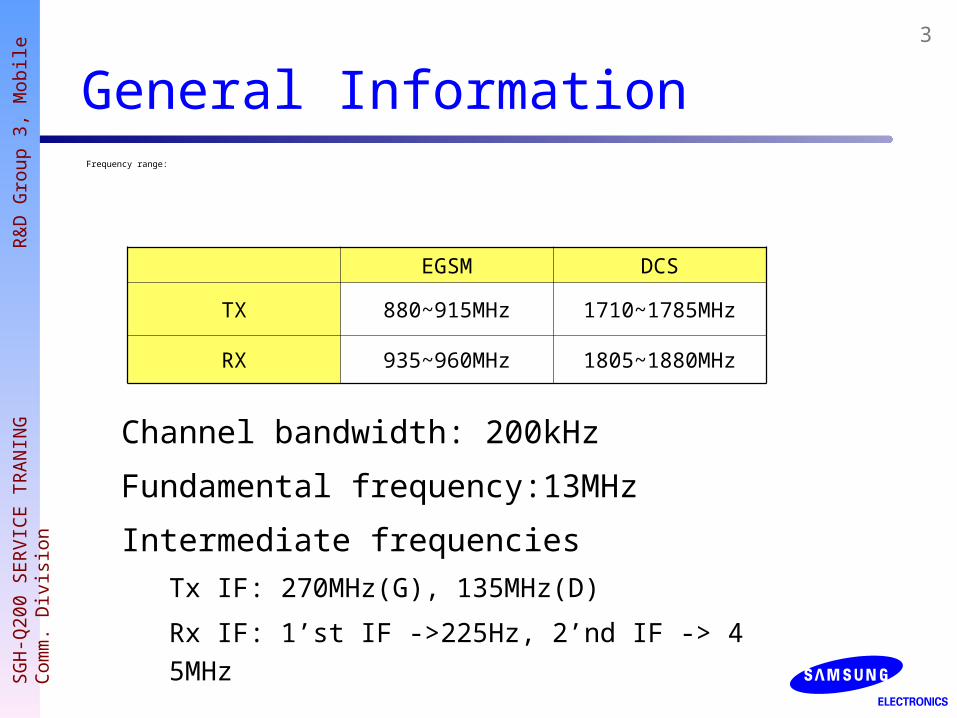
Frequency range:
General Information
EGSM DCS
TX 880~915MHz 1710~1785MHz
RX 935~960MHz 1805~1880MHz
Channel bandwidth: 200kHz
Fundamental frequency:13MHz
Intermediate frequenciesTx IF: 270MHz(G), 135MHz(D)
Rx IF: 1’st IF ->225Hz, 2’nd IF -> 45MHz

4SG
H-Q
200 S
ER
VIC
E T
RA
NIN
G
R&
D G
roup
3, M
obile
Com
m.
Div
isio
n
General Information
Solution : Agere system(Lucent technology)
Design : Dual folder
LCD : 128 x 128
Memory : 48M/4M
Size and Weight :85(H)x47(W)x19.8(D), 90g
Funtion : GPRS Class 8, EFR/FR, WAP, GAME ..etc
Operating Time
Talk TIME Stand by TIME
SLIM(720mA) Up to 150min Up to 70 hr
STANDARD(900mA)
Up to 180min Up to 85 hr
5SG
H-Q
200 S
ER
VIC
E T
RA
NIN
G
R&
D G
roup
3, M
obile
Com
m.
Div
isio
n
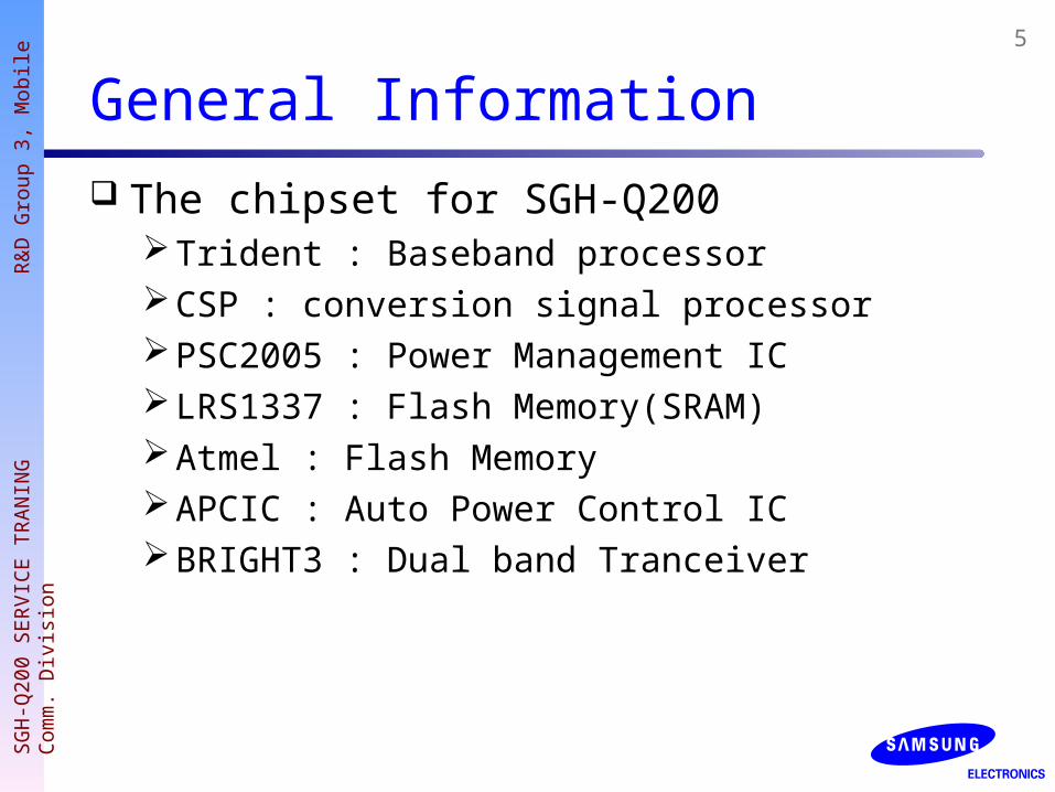
The chipset for SGH-Q200Trident : Baseband processorCSP : conversion signal processorPSC2005 : Power Management ICLRS1337 : Flash Memory(SRAM)Atmel : Flash MemoryAPCIC : Auto Power Control ICBRIGHT3 : Dual band Tranceiver
General Information
6SG
H-Q
200 S
ER
VIC
E T
RA
NIN
G
R&
D G
roup
3, M
obile
Com
m.
Div
isio
n
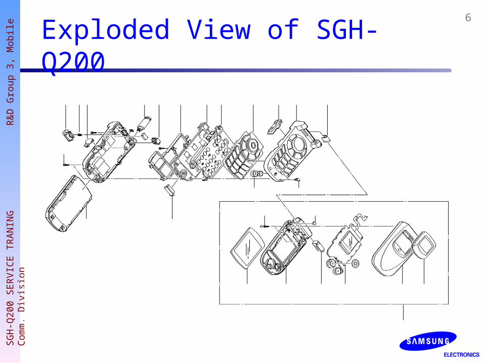
Exploded View of SGH-Q200

7SG
H-Q
200 S
ER
VIC
E T
RA
NIN
G
R&
D G
roup
3, M
obile
Com
m.
Div
isio
n
Top View of SGH-Q200

8SG
H-Q
200 S
ER
VIC
E T
RA
NIN
G
R&
D G
roup
3, M
obile
Com
m.
Div
isio
n
Bottom View of SGH-Q200

9SG
H-Q
200 S
ER
VIC
E T
RA
NIN
G
R&
D G
roup
3, M
obile
Com
m.
Div
isio
n
Block Diagram (Radio Part)
Antenna
FEM
LNA
LNA
RF
FILTER
RF
FILTER
LPF
LPF
RX
SAW
RX
SAW
MIXER 1
MIXER 2
IF
SAW
225MHz270MHz
LC
FILTER
1/2
1/2
IF VCO
RF
SYNTH
IF
SYNTH
RF VCO
TX VCO
LOOP
FILTERPD
I,Q
MODULATOR
1080MHz
GSM :1150MHz~1185MHz
DCS:RX:1580MHz~1655MHz
TX:1575MHz~1650MHz
DCS:270MHz
GSM:540MHzSWITCH
1/2
1/2
45MHz
PGAI,Q
DEMOD
SERIAL DATA
INTERFACE
1/6
GSM:270MHz
DCS:135MHz
GSM:270MHz
DCS:135MHz
GSM:880MHz~915MHz
DCS:1710MHz~1785MHz
GSM:880MHz~915MHz
DCS:1710MHz~1785MHz
PAM
GSM:925MHz~960MHz
DCS:1805MHz~1880MHz
I,Q
I,Q
CSP1089
OCTL
SIGNALS
TRIDENT
RF
DRIVER
DSP JTAG
DAI
DSP16000
ARM7TDMI
UIAUDIO
SERIAL
DATA,
CLK,
LE
10SG
H-Q
200 S
ER
VIC
E T
RA
NIN
G
R&
D G
roup
3, M
obile
Com
m.
Div
isio
n
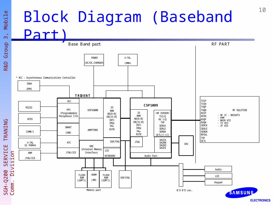
Block Diagram (Baseband Part)
TRIDENT
B'D B'D con.
Audio
Keypad
LCD
Memory part
SIM0/1
X-TAL32.768KHz
RF SOLUTION
- RF IC : BRIGHT3- PAM- MAIN VCO- TX VCO- IF VCO
GPIO
POWER
(DC/DC,CHARGER)
X-TAL
13MHz
RS232CSP1089
Audio Part
LCD
KEYBOARD
SRAM
(4M)
FLASHROM
(16M*1)
EMI(External Memory
Interface)
TXIPTXINTXQPTXQNRXIPRXINRXQPRXQNSERCKSERLESERDARFOVLTXPOCTL
<RF DIRVER>TXI/QRX I/QTXPSERCKSERLESERDA
OCTL[1:11]
IORWN
AB[8:0]DB[15:0]INT1IRQxPAxRSTB
IORWN
AB[8:0]DB[15:0]INT1IRQxPAxRSTB
ARM
JTAG/ICE
DAICKDAIRNDAIDODAIDI
DAIDSPJTAG JTAG
DSPJTAG
IRDA
GPRS
ACC
PPI(ProgrammablePeripheral I/O)
RTC
SMART
CARD
JTAG/ICE
* ACC : Asynchronous Communications Controller
DSP16000
ARM7TDMI
FLASHROM
(32M*1)
RF PARTBase Band part

11SG
H-Q
200 S
ER
VIC
E T
RA
NIN
G
R&
D G
roup
3, M
obile
Com
m.
Div
isio
n
Circuit Description: Front-End
1. Antenna (ANT1002) Transmitting and Receiving the information
desired from air interface.
2. RF Test Switch (CN1001) This is for adjusting and testing the
handset in conjunction with the test equipment such as HP8922M or HP8960.
3. Diplexer (U1006) It operates such like a combination of Rx
filter and Tx filter, and provides agreeable isolation between Tx and Rx.

12SG
H-Q
200 S
ER
VIC
E T
RA
NIN
G
R&
D G
roup
3, M
obile
Com
m.
Div
isio
n
Circuit Description: Rx
1. LNA It amplifies weak signal by 14~20dB without
increasing the noise significantly. This provides “Step Gain AGC” of ~35dB so that it supplements narrow dynamic range of Rx AGC.
2. RF Rx SAW Filter (F901:GSM , F903:DCS) It has the bandwidth of Rx frequencies, and
suppresses interferers which can do affect the IF signal
3. 1st Down-conversion Mixer Received RF carrier is converted to 1st IF (225MHz).
Local signal is needed for frequency mixing. It has ~9dB conversion gain, in general.

13SG
H-Q
200 S
ER
VIC
E T
RA
NIN
G
R&
D G
roup
3, M
obile
Com
m.
Div
isio
n
Circuit Description: Rx
1. IF SAW Filter (F902) Center frequency is 225MHz. It suppresses
unwanted image signals made in the 1st mixer
2. 2nd Down-conversion Mixer 1st IF is converted to 2nd IF of 45MHz..
3. 2nd IF LC Filter It has 200kHz bandwidth with 45MHz center
frequency. It attenuates images from the 2nd mixer
4. RSSI It produces DC voltage according to the received
signal strength.

14SG
H-Q
200 S
ER
VIC
E T
RA
NIN
G
R&
D G
roup
3, M
obile
Com
m.
Div
isio
n
Circuit Description: Rx
1. PGA Sets the programmable gain array to one
of 50 values separated by 2dB [000000] ~[110001]

15SG
H-Q
200 S
ER
VIC
E T
RA
NIN
G
R&
D G
roup
3, M
obile
Com
m.
Div
isio
n
Circuit Description: Rx - Digital1. Rx AGC
The purpose of Rx AGC is to maintain the Rx I/Q voltage level, regardless of the received signal strength. In general, Rx AGC has the dynamic range of around 70dB..
2. Rx I/Q Demodulator It generates both in-phase (I) and quadrature (Q) c
omponents of the signal while translating the IF signal to baseband.

16SG
H-Q
200 S
ER
VIC
E T
RA
NIN
G
R&
D G
roup
3, M
obile
Com
m.
Div
isio
n
Circuit Description: Local1. VC-TCXO (OSC801)
13MHz fundamental frequency for PLLs and Baseband chipset (U601).2. RF VCO (OSC901)
It supplies Local source frequency higher than RF carrier by 225MHz in conjunction with PLL(GSM)
Lower than RF carrier by 225MHz in conjuntion with PLL(DCS) Higher than Tx RF carrier by 270MHz in conjuntion with PLL
3. IF VCO (OSC902) It generates 1080MHz frequency for up-converting Tx I/Q signal to Tx I
F and Rx signal to RxIF4. TX VCO (OSC903)
Frequency : 880~915MHz(G), 1710~1785MHz(D)

17SG
H-Q
200 S
ER
VIC
E T
RA
NIN
G
R&
D G
roup
3, M
obile
Com
m.
Div
isio
n
Circuit Description: Tx
1.Tx I/Q modulator Tx I and Q signals are combined and up-converted
to 270(G),135(D)MHz frequency. I, Q voltage levels are 1Vp-p, respectively.
2.PAM (U1002) It increases Tx power level so that PA is capable
of transmitting the maximum power up to 35dBm High gain 3stage amplifier: 0dBm input Typ 2in/2out dual band amplifier One power control pin with one band switch

18SG
H-Q
200 S
ER
VIC
E T
RA
NIN
G
R&
D G
roup
3, M
obile
Com
m.
Div
isio
n
Circuit Description: Tx
1. APCIC (U1001) Dual Band Power control IC for TX power Amp has ~55 dB dynamic range, Contains power detector and operantional Amp
converts RF power into DC level.
2. Coupler :F1001(G), F1002(D) The coupling factor is 14dB,20dB. That is, “P(PA
output) – 14dB,-20dB” is transmitted to the power detector circuitry

19SG
H-Q
200 S
ER
VIC
E T
RA
NIN
G
R&
D G
roup
3, M
obile
Com
m.
Div
isio
n
Circuit Description: Logic
TRIDENT (U601) Baseband Engine Includes the DSP16000 core,ARM7TDMI microcontroller cor
e,and a standard sets of peripherals for the DSP and ARM communicates with Memory, Keypad, LCD, and other periph
erals DSP RAM :20k x 16 DSP ROM : 144k x 16 ARM RAM : 2k x 32 RAM(byte writable) ARM ROM : 4k x 32 ROM(mask-programmable) Processor Interface memory : 512 x 16 shared RAM
20SG
H-Q
200 S
ER
VIC
E T
RA
NIN
G
R&
D G
roup
3, M
obile
Com
m.
Div
isio
n
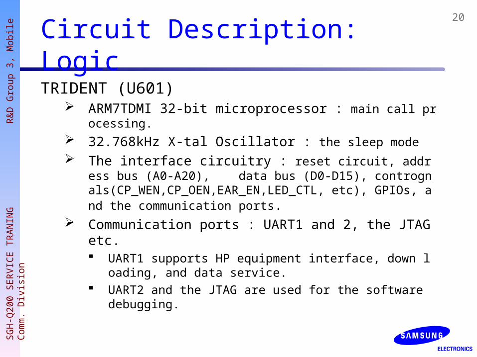
Circuit Description: Logic
TRIDENT (U601) ARM7TDMI 32-bit microprocessor : main call processing. 32.768kHz X-tal Oscillator : the sleep mode The interface circuitry : reset circuit, address bus (A0-A20), d
ata bus (D0-D15), contrognals(CP_WEN,CP_OEN,EAR_EN,LED_CTL, etc), GPIOs, and the communication ports.
Communication ports : UART1 and 2, the JTAG etc. UART1 supports HP equipment interface, down loading, and da
ta service. UART2 and the JTAG are used for the software debugging.
21SG
H-Q
200 S
ER
VIC
E T
RA
NIN
G
R&
D G
roup
3, M
obile
Com
m.
Div
isio
n
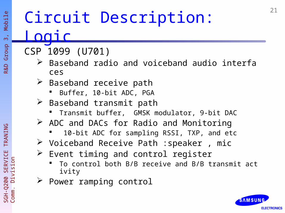
Circuit Description: Logic
CSP 1099 (U701) Baseband radio and voiceband audio interfaces Baseband receive path
Buffer, 10-bit ADC, PGA Baseband transmit path
Transmit buffer, GMSK modulator, 9-bit DAC ADC and DACs for Radio and Monitoring
10-bit ADC for sampling RSSI, TXP, and etc Voiceband Receive Path :speaker , mic Event timing and control register
To control both B/B receive and B/B transmit activity Power ramping control

22SG
H-Q
200 S
ER
VIC
E T
RA
NIN
G
R&
D G
roup
3, M
obile
Com
m.
Div
isio
n
Circuit Description: Logic
PMIC(PSC2005:U101) Includes six low-dropout voltage regulator
LDO1-1.8v, LDO2:VCCD, LDO3:Vrf LDO4-Vapc,LDO5:Vosc/syn,LDO6:VCCA
250ms system reset generator To ensure proper initialization of the system controller
12bit monotonic DAC Pwr_sw1,Pwr_sw2,CS => active low.

23SG
H-Q
200 S
ER
VIC
E T
RA
NIN
G
R&
D G
roup
3, M
obile
Com
m.
Div
isio
n
Circuit Description: Logic
Flash memory Flash ROM:U501(32M x 1),U1010(16M x1)
The 48Mbit FLASH ROM is used to store code of the application program. Using the down-loader program, this application program can be changed even after the mobile is fully assembled.
SRAM The 4Mbit SRAM is used to store the internal flag
information, call processing data, and timer data.

24SG
H-Q
200 S
ER
VIC
E T
RA
NIN
G
R&
D G
roup
3, M
obile
Com
m.
Div
isio
n
Circuit Description: Logic Power On
Press of END key BATT and POW_ON signals are connected Q204 turn-on Q102 turn-on, that is, BATT is connected to VBAT VBAT is supplied to U101 VCCD and VCCA are applied to U101, U601 VCTCXO signal is enabled VC-TCXO (OSC801) is operating Once U601 runs without error, U601 enables POWER_KEEP signal
Power Off Press of END key Q204 turn-on U601
checks BB_PWR turns logic high to low Main application program enter to Power Off mode

25SG
H-Q
200 S
ER
VIC
E T
RA
NIN
G
R&
D G
roup
3, M
obile
Com
m.
Div
isio
n
Circuit Description: Logic
Key Pad The Key Pad is belong to main board. For key-press r
ecognition, the structure of key is consisted of 5 x 5 matrix, which is used input signal key_col(0-4) and output signal key_row(0-4) of Trident.
LCD MODULE LCD module is connected to main board by FPCB. T
his contains an LCD controller. An LCD controller controls the information of displaying from the Trident (parallel 8-bit data) to the LCD.

26SG
H-Q
200 S
ER
VIC
E T
RA
NIN
G
R&
D G
roup
3, M
obile
Com
m.
Div
isio
n
Test Interface Jig
Data cable
Test cable
27SG
H-Q
200 S
ER
VIC
E T
RA
NIN
G
R&
D G
roup
3, M
obile
Com
m.
Div
isio
n
TE
ST
PA
CK
TDMA I/F TEST JIG
POWERON/OFF
TOA-IN
TOA-OUT
- +DC 4.0V
SAMSUNG
TO
.PC
TO
.HP
AUTOON/OFF
BOOTON/OFF
UARTU1-U2
COMPort
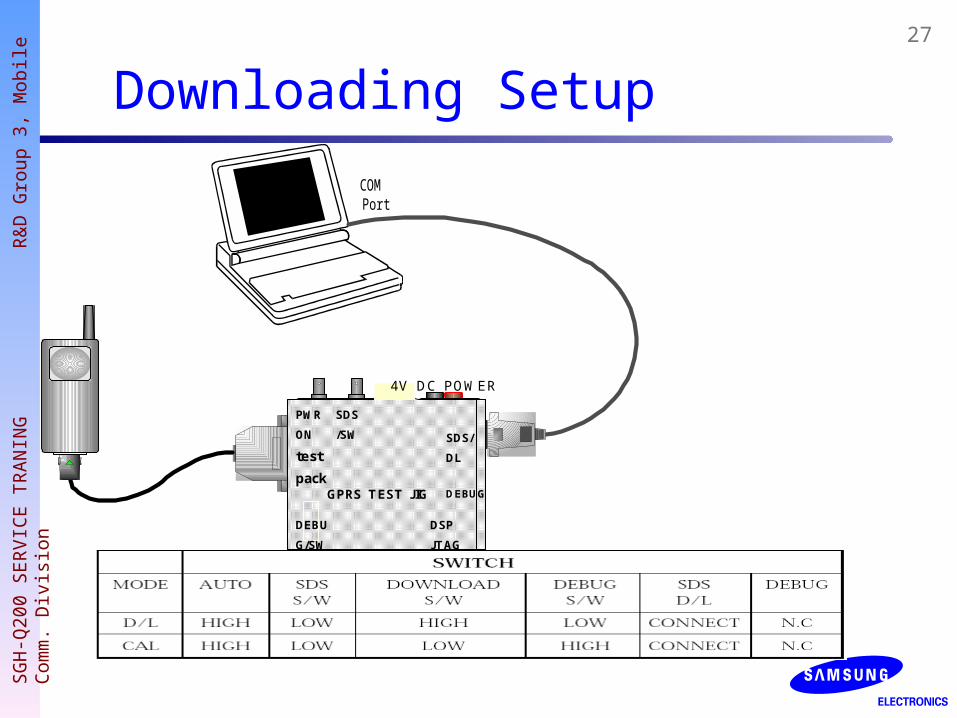
Downloading Setup
test
pack
SDS/
DL
PWR
ON
SDS
/SW
DEBU
G/SW
DSP
JTAG
GPRS TEST JIG
4V DC POWER
DEBUG

28SG
H-Q
200 S
ER
VIC
E T
RA
NIN
G
R&
D G
roup
3, M
obile
Com
m.
Div
isio
n
Auto calibration Program Setting
TE
ST
PA
CK
TDMA I/F TEST JIG
POWERON/OFF
TOA-IN
TOA-OUT
- +DC 4.0V
SAMSUNG
TO
.PC
TO
.HP
AUTOON/OFF
BOOTON/OFF
UARTU1-U2
COMPort
test
pack
SDS/
DL
PWR
ON
SDS
/SW
DEBU
G/SW
DSP
JTAG
GPRS TEST JIG
4V DC POWER
DEBUG
HP8960
POWER
SUPPLY
GPIB CABLE
GPIB CARD
E3632A
HP

29SG
H-Q
200 S
ER
VIC
E T
RA
NIN
G
R&
D G
roup
3, M
obile
Com
m.
Div
isio
n
Auto calibration Processing
30SG
H-Q
200 S
ER
VIC
E T
RA
NIN
G
R&
D G
roup
3, M
obile
Com
m.
Div
isio
n
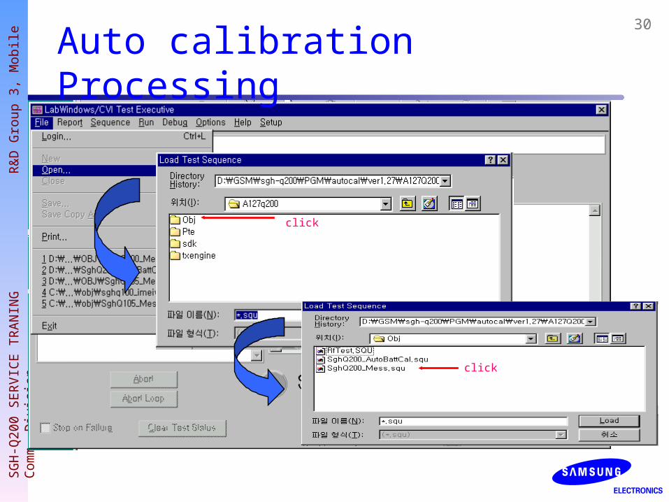
Auto calibration Processing
click
click
click

31SG
H-Q
200 S
ER
VIC
E T
RA
NIN
G
R&
D G
roup
3, M
obile
Com
m.
Div
isio
n
Auto calibration Processing
click

32SG
H-Q
200 S
ER
VIC
E T
RA
NIN
G
R&
D G
roup
3, M
obile
Com
m.
Div
isio
n
Auto calibration Processing
click
33SG
H-Q
200 S
ER
VIC
E T
RA
NIN
G
R&
D G
roup
3, M
obile
Com
m.
Div
isio
n
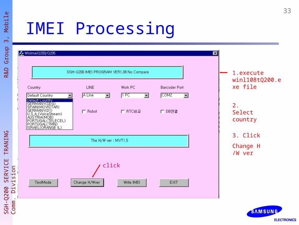
IMEI Processing
1.execute winl108tQ200.exe file
2. Select country
3. Click
Change H/W ver
click

34SG
H-Q
200 S
ER
VIC
E T
RA
NIN
G
R&
D G
roup
3, M
obile
Com
m.
Div
isio
n
IMEI Processing
1.write H/W ver
2.click write IMEI

35SG
H-Q
200 S
ER
VIC
E T
RA
NIN
G
R&
D G
roup
3, M
obile
Com
m.
Div
isio
n
IMEI Processing
1.click
2.write imei
3.click
4.click
36SG
H-Q
200 S
ER
VIC
E T
RA
NIN
G
R&
D G
roup
3, M
obile
Com
m.
Div
isio
n
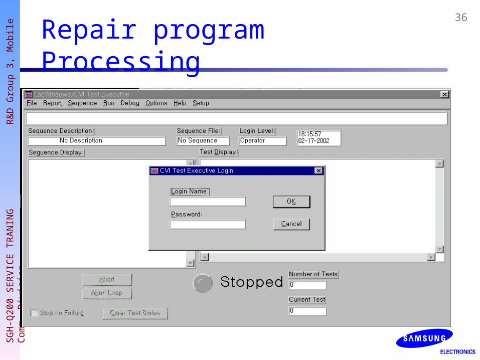
Repair program Processing
37SG
H-Q
200 S
ER
VIC
E T
RA
NIN
G
R&
D G
roup
3, M
obile
Com
m.
Div
isio
n
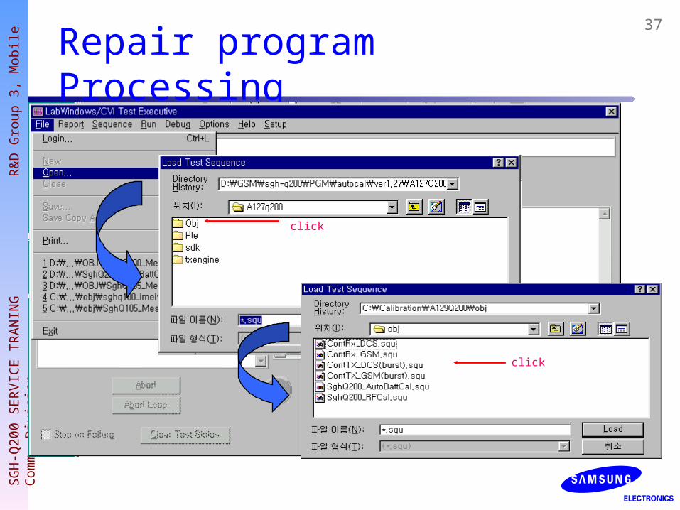
Repair program Processing
click
click
38SG
H-Q
200 S
ER
VIC
E T
RA
NIN
G
R&
D G
roup
3, M
obile
Com
m.
Div
isio
n
Repair program Processing

39SG
H-Q
200 S
ER
VIC
E T
RA
NIN
G
R&
D G
roup
3, M
obile
Com
m.
Div
isio
n
Repair program Processing
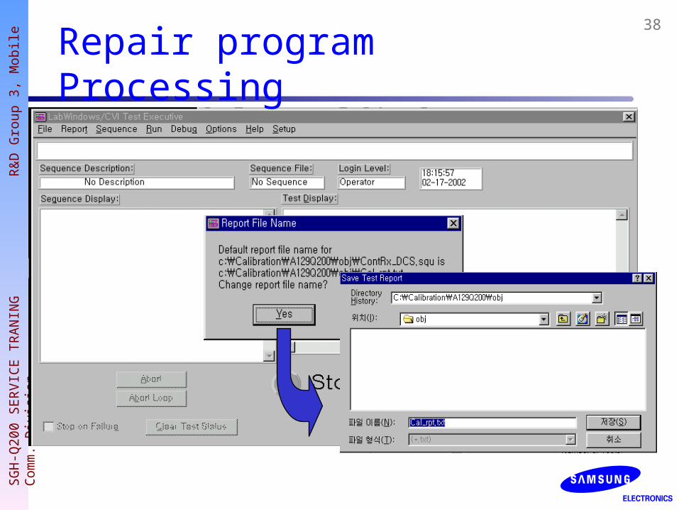
click

40SG
H-Q
200 S
ER
VIC
E T
RA
NIN
G
R&
D G
roup
3, M
obile
Com
m.
Div
isio
n
Phone Test Setup
TE
ST
PA
CK
GPRS TEST JIG
POWERON
SDSS/W
- +DC 4.0V
SAMSUNG
DE
BU
GSD
S D/L
DEBUGS/W
DSPJTAG
HP8960
Power SupplyRF Test Cable
GPIB CABLE
PC
Com1 port
Gpib cardt
41SG
H-Q
200 S
ER
VIC
E T
RA
NIN
G
R&
D G
roup
3, M
obile
Com
m.
Div
isio
n
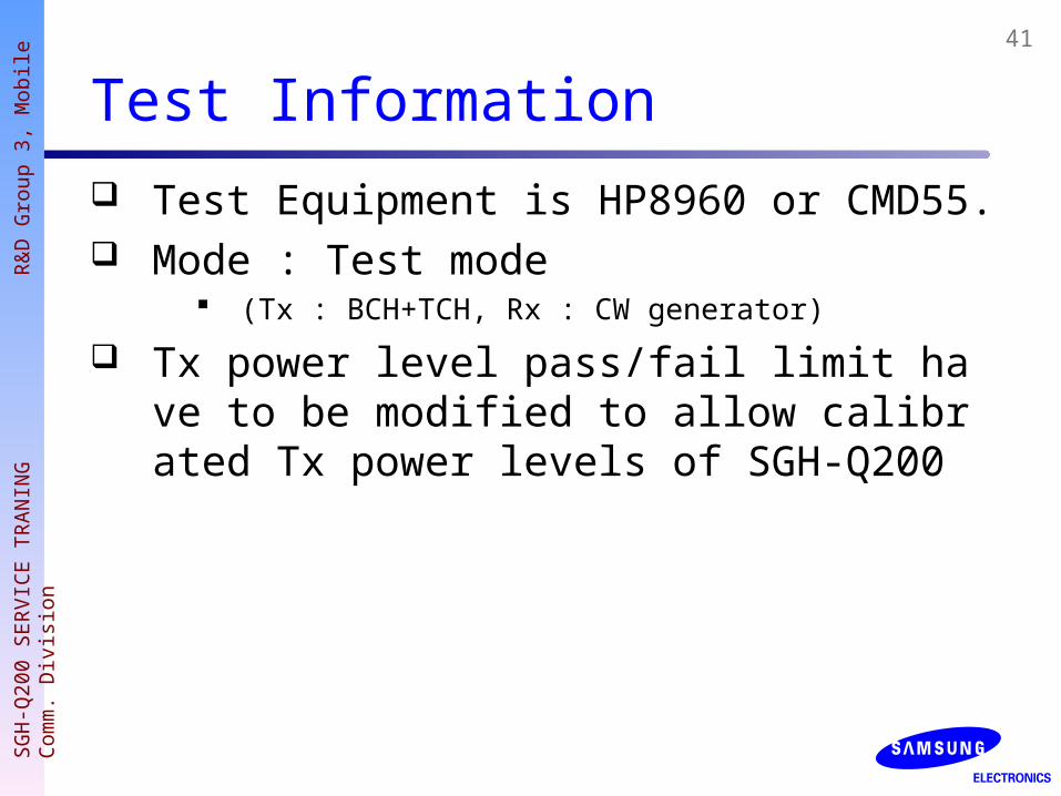
Test Information Test Equipment is HP8960 or CMD55. Mode : Test mode
(Tx : BCH+TCH, Rx : CW generator)
Tx power level pass/fail limit have to be modified to allow calibrated Tx power levels of SGH-Q200
42SG
H-Q
200 S
ER
VIC
E T
RA
NIN
G
R&
D G
roup
3, M
obile
Com
m.
Div
isio
n
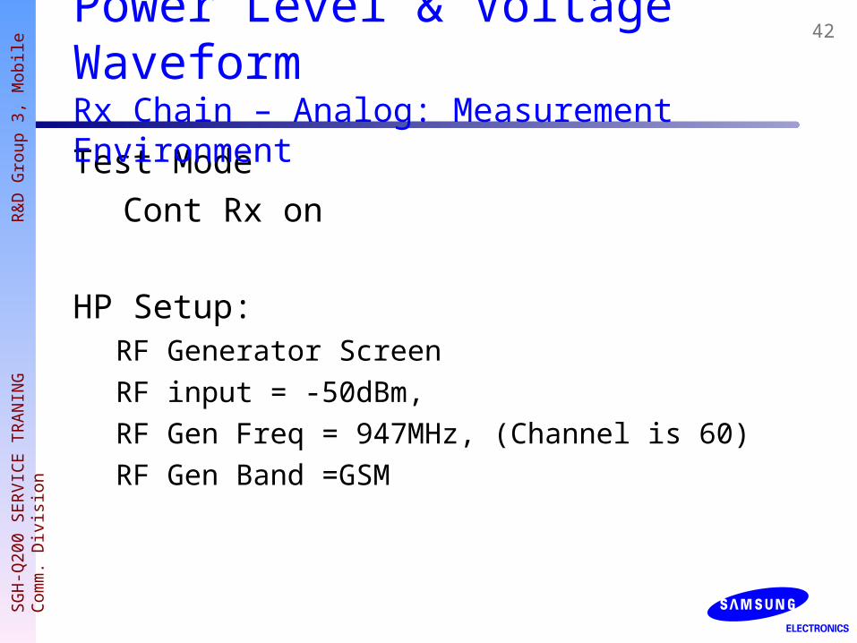
Test ModeCont Rx on
HP Setup: RF Generator ScreenRF input = -50dBm, RF Gen Freq = 947MHz, (Channel is 60)RF Gen Band =GSM
Power Level & Voltage Waveform Rx Chain – Analog: Measurement Environment

43SG
H-Q
200 S
ER
VIC
E T
RA
NIN
G
R&
D G
roup
3, M
obile
Com
m.
Div
isio
nPower Level & Voltage Waveform
Rx ChainAntenna
FEM
LNA
LNA
RF
FILTER
RF
FILTER
LPF
LPF
RX
SAW
RX
SAW
MIXER 1
MIXER 2
IF
SAW
225MHz270MHz
LC
FILTER
1/2
1/2
IF VCO
RF
SYNTH
IF
SYNTH
RF VCO
TX VCO
LOOP
FILTERPD
I,Q
MODULATOR
1080MHz
GSM :1150MHz~1185MHz
DCS:RX:1580MHz~1655MHz
TX:1575MHz~1650MHz
DCS:270MHz
GSM:540MHzSWITCH
1/2
1/2
45MHz
PGAI,Q
DEMOD
SERIAL DATA
INTERFACE
1/6
GSM:270MHz
DCS:135MHz
GSM:270MHz
DCS:135MHz
GSM:880MHz~915MHz
DCS:1710MHz~1785MHz
GSM:880MHz~915MHz
DCS:1710MHz~1785MHz
PAM
GSM:925MHz~960MHz
DCS:1805MHz~1880MHz
I,Q
I,Q
CSP1089
OCTL
SIGNALS
TRIDENT
RF
DRIVER
DSP JTAG
DAI
DSP16000
ARM7TDMI
UIAUDIO
SERIAL
DATA,
CLK,
LE
Ant s/w In
LNA In LNA out

44SG
H-Q
200 S
ER
VIC
E T
RA
NIN
G
R&
D G
roup
3, M
obile
Com
m.
Div
isio
nPower Level & Voltage Waveform
Rx ChainAntenna
FEM
LNA
LNA
RF
FILTER
RF
FILTER
LPF
LPF
RX
SAW
RX
SAW
MIXER 1
MIXER 2
IF
SAW
225MHz270MHz
LC
FILTER
1/2
1/2
IF VCO
RF
SYNTH
IF
SYNTH
RF VCO
TX VCO
LOOP
FILTERPD
I,Q
MODULATOR
1080MHz
GSM :1150MHz~1185MHz
DCS:RX:1580MHz~1655MHz
TX:1575MHz~1650MHz
DCS:270MHz
GSM:540MHzSWITCH
1/2
1/2
45MHz
PGAI,Q
DEMOD
SERIAL DATA
INTERFACE
1/6
GSM:270MHz
DCS:135MHz
GSM:270MHz
DCS:135MHz
GSM:880MHz~915MHz
DCS:1710MHz~1785MHz
GSM:880MHz~915MHz
DCS:1710MHz~1785MHz
PAM
GSM:925MHz~960MHz
DCS:1805MHz~1880MHz
I,Q
I,Q
CSP1089
OCTL
SIGNALS
TRIDENT
RF
DRIVER
DSP JTAG
DAI
DSP16000
ARM7TDMI
UIAUDIO
SERIAL
DATA,
CLK,
LE
Mixer In
IF SAW
Out
Mixer out

45SG
H-Q
200 S
ER
VIC
E T
RA
NIN
G
R&
D G
roup
3, M
obile
Com
m.
Div
isio
nPower Level & Voltage Waveform
Rx ChainAntenna
FEM
LNA
LNA
RF
FILTER
RF
FILTER
LPF
LPF
RX
SAW
RX
SAW
MIXER 1
MIXER 2
IF
SAW
225MHz270MHz
LC
FILTER
1/2
1/2
IF VCO
RF
SYNTH
IF
SYNTH
RF VCO
TX VCO
LOOP
FILTERPD
I,Q
MODULATOR
1080MHz
GSM :1150MHz~1185MHz
DCS:RX:1580MHz~1655MHz
TX:1575MHz~1650MHz
DCS:270MHz
GSM:540MHzSWITCH
1/2
1/2
45MHz
PGAI,Q
DEMOD
SERIAL DATA
INTERFACE
1/6
GSM:270MHz
DCS:135MHz
GSM:270MHz
DCS:135MHz
GSM:880MHz~915MHz
DCS:1710MHz~1785MHz
GSM:880MHz~915MHz
DCS:1710MHz~1785MHz
PAM
GSM:925MHz~960MHz
DCS:1805MHz~1880MHz
I,Q
I,Q
CSP1089
OCTL
SIGNALS
TRIDENT
RF
DRIVER
DSP JTAG
DAI
DSP16000
ARM7TDMI
UIAUDIO
SERIAL
DATA,
CLK,
LE
2’nd mixer out

46SG
H-Q
200 S
ER
VIC
E T
RA
NIN
G
R&
D G
roup
3, M
obile
Com
m.
Div
isio
nPower Level & Voltage Waveform
Tx Chain Active Cell mode
HP Setup RF input = -50dBm,
TCH Channel = 60CHRF Gen Band = GSM

47SG
H-Q
200 S
ER
VIC
E T
RA
NIN
G
R&
D G
roup
3, M
obile
Com
m.
Div
isio
nPower Level & Voltage Waveform
Tx ChainAntenna
FEM
LNA
LNA
RF
FILTER
RF
FILTER
LPF
LPF
RX
SAW
RX
SAW
MIXER 1
MIXER 2
IF
SAW
225MHz270MHz
LC
FILTER
1/2
1/2
IF VCO
RF
SYNTH
IF
SYNTH
RF VCO
TX VCO
LOOP
FILTERPD
I,Q
MODULATOR
1080MHz
GSM :1150MHz~1185MHz
DCS:RX:1580MHz~1655MHz
TX:1575MHz~1650MHz
DCS:270MHz
GSM:540MHzSWITCH
1/2
1/2
45MHz
PGAI,Q
DEMOD
SERIAL DATA
INTERFACE
1/6
GSM:270MHz
DCS:135MHz
GSM:270MHz
DCS:135MHz
GSM:880MHz~915MHz
DCS:1710MHz~1785MHz
GSM:880MHz~915MHz
DCS:1710MHz~1785MHz
PAM
GSM:925MHz~960MHz
DCS:1805MHz~1880MHz
I,Q
I,Q
CSP1089
OCTL
SIGNALS
TRIDENT
RF
DRIVER
DSP JTAG
DAI
DSP16000
ARM7TDMI
UIAUDIO
SERIAL
DATA,
CLK,
LE
TxIP
TXEN1
Tx locking
0.8~2.5V

48SG
H-Q
200 S
ER
VIC
E T
RA
NIN
G
R&
D G
roup
3, M
obile
Com
m.
Div
isio
n
Voltage Waveforms: Local
OSC901RF Local @ 62CH
OSC902IF Local

49SG
H-Q
200 S
ER
VIC
E T
RA
NIN
G
R&
D G
roup
3, M
obile
Com
m.
Div
isio
n
Voltage Waveforms: Logic
OSC801.413MHz TCXO Out
osc60132.768kHz clock

50SG
H-Q
200 S
ER
VIC
E T
RA
NIN
G
R&
D G
roup
3, M
obile
Com
m.
Div
isio
n
Repair Examplesproblems Reason
call fail
Vrf tantal osillation
C973,C974 open
ant path 0ohm open
AFC fail
VC- TCXO crack (abnormal operation)
CSP1099 chip problem
broken CN1001
GSM RX gain fail poorly made RF SAW(F1003):4dB loss
no buzzer sound poor soldering of AU501
no speaker sound
LCD FPCB 16,18pin short
speaker wire open
poorly made speaker
no mic sound contact problem(not connect)
power on fail
OSC801(VC- TCXO)
OSC601(32.768KHz)
poorly made U601(Trident) &poorly
soldering
U1010(atmel memory)problem & crack
collapse batt pin
no rssi bar poorly made OSC801(vc- tcxo)
no vibration be folded motor wire
no key toneOSC601 crack
poorly made key pad
RTC x- tal(32.768KHz) crack
51SG
H-Q
200 S
ER
VIC
E T
RA
NIN
G
R&
D G
roup
3, M
obile
Com
m.
Div
isio
n
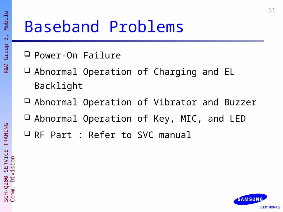
Baseband Problems
Power-On Failure
Abnormal Operation of Charging and EL
Backlight
Abnormal Operation of Vibrator and Buzzer
Abnormal Operation of Key, MIC, and LED
RF Part : Refer to SVC manual
52SG
H-Q
200 S
ER
VIC
E T
RA
NIN
G
R&
D G
roup
3, M
obile
Com
m.
Div
isio
n
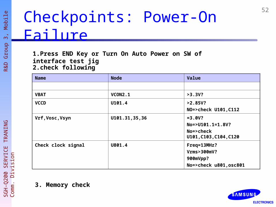
Checkpoints: Power-On Failure
1.Press END Key or Turn On Auto Power on SW of interface test jig2.check following
Name Node Value
VBAT VCON2.1 >3.3V?
VCCD U101.4 >2.85V?NO=>check U101,C112
Vrf,Vosc,Vsyn U101.31,35,36 =3.0V?No=>U101.1=1.8V?No=>check U101,C103,C104,C120
Check clock signal U801.4 Freq=13MHz?Vrms>300mV?900mVpp?No=>check u801,osc801
3. Memory check

53SG
H-Q
200 S
ER
VIC
E T
RA
NIN
G
R&
D G
roup
3, M
obile
Com
m.
Div
isio
n
Checkpoints: Charging and EL Backlight
Charging
EL BacklightName Node
DesirableValue
LED_CTL Q301.1 highQ301.3 low
BAKLIGHT CN202.12 low
Name NodeDesirable
Value
VEXT CN301.17,18around 4.5V? No=>
replace TA
Q205.3
lowno=>check
Q201,U201,C203,R203
CHG_ON U202.2,5,6high
no=>change u202
U202.3 low
U201.53.2V~4.2V?
No=>change201

54SG
H-Q
200 S
ER
VIC
E T
RA
NIN
G
R&
D G
roup
3, M
obile
Com
m.
Div
isio
n
Checkpoints: Vibrator and Buzzer
Name NodeDesirable
ValueRINGER R508,Q502.3 PWM SignalVBAT C506 >3.3V
Au501.3 PWM SignalBuzzer Impedance AU501.3 to 4 ~15 Ohm
Name NodeDesirable
ValueMotor_en Q503.2 3V
VBAT Q501.2 3V- CN202.5 3V
Vibrator
Buzzer

55SG
H-Q
200 S
ER
VIC
E T
RA
NIN
G
R&
D G
roup
3, M
obile
Com
m.
Div
isio
n
Checkpoints: Key, MIC, and LED
Key recognition check1. Metal Dome Array2. CN202 pin#1,2,3, and 43. VCTCXO_IN (C807)
MIC check1. MIC400 contact2. U401 pin#1,2,and5
LED check1. Control signal =>keypad LED: LED_CTL, =>SVC_LED:
SVC_LED(Q601.2:high,Q601.3:low)
1. VCC

56SG
H-Q
200 S
ER
VIC
E T
RA
NIN
G
R&
D G
roup
3, M
obile
Com
m.
Div
isio
n
Thank you!!