seu - european space agencymicroelectronics.esa.int/finalreport/at697f-summary...table of figures...
TRANSCRIPT
®
AT697F LEON2FT FM SPARC V8 space processor
Summary Report
Version 3.0 – 08/08/2012
Reference: ADF-MK-R1011-MLN
ESA Contract 19083/05/NL/FM – Call-off order 002 CNES contract 721/00/8386/02
PROPRIETARY INFORMATION ALL INFORMATION DISCLOSED IN THIS DOCUMENT ARE CONFIDENTIAL AND FOR
INTERNAL USE ONLY
Atmel Nantes S.A. La Chantrerie BP 70602 44306 Nantes Cedex 03 France Tel.: 33 (0) 2 40 18 18 18 Fax.: 33 (0) 2 40 18 19 20 http://www.atmel.com

®
Page left intentionally blank
AT697F summary report V3.0 08/08/2012 ADF-MK-R1011-MLN Page 2

®
1 Abstract This document presents a summary of the activities performed and of the results obtained during the LEON2-FT Flight model development. This LEON2-FT Flight model has been made available by ATMEL with the product name AT697F. After the development of the AT697E (LEON2-FT prototype) processor under the ESA contract 15036/01/NL/FM, a new design phase for the AT697 flight model started under the ESA Contract 19083/05/NL/FM – Call-off order 002 and the CNES contract 721/00/8386/02 started in July 2006. After a design phase of more than 2 years the design was released to fab in 2008 (tape to fab). The first silicon of AT697F (LEON2-FT FM) processor was available for the beta tester and for European Space community early 2009. After the characterisation and the radiation testing performed from 2009 to 2010 followed by the functional validation, the evaluation and qualification performed in 2011 the first flight model was delivered to customer end of 2011. It is a first pass yield meaning no redesign has been necessary.
- The AT697F is fully functional, only one bug found at the very late stage of the design remains it was commonly agreed not to delay the design phase. - The AT697F fully works over the whole bias and military temperature ranges. - The AT697F has been tested successfully up to a total dose of 300 Krad(Si). - The AT697F is a SEU/SET hardened processor, the error rate in space for the GEO orbit (worst
case) has been calculated at one no-correctable error for more than 100 years. - the Single Event Latch-up tests at 70 MeV/mg/cm² have been performed on other test vehicle in
the same manufacturing process (AT58KRHA) therefore only a test at 60 MeV/mg/cm2 at 125°C has been performed on AT697F
The main milestones are shown in the timeline below:
1998 1999 2000 2001 2002 2003 2004 2005 2006 2007 2008 2009 2010 2011 2012
Preparation:LEON-Express
Demonstrator (350 nm)
Designtape-out:Jan. 2001
March:SEU test
AT697Econtract15036
15. FebKick-offPhase 1
30. Oct.ATP phase 2
= AT697E
Design workUpdates ofLEON2FT
10. DecTape-outAT697E
Functional& Radiation
Testing
EvaluationAlphaUsers
Design intoPROBA-2
& ERNO-box
Feb.ERNO-box
launch to ISS
2. NovLaunch ofProba-2
AT697Fcontract19038
4. JulyKick-off
Design workUpdates ofLEON2FT
6. JuneTape-outAT697F
Validation,Evaluation &qualification
25. April:Final
Presentation
Round-tables and preparation meetings
Test & characterisationTotal dose & SEE testing
Figure 1: AT697 Project Timeline
AT697F summary report V3.0 08/08/2012 ADF-MK-R1011-MLN Page 3

®
Page left intentionally blank
AT697F summary report V3.0 08/08/2012 ADF-MK-R1011-MLN Page 4

®
TABLE OF CONTENTS
1 Abstract ............................................................................................................... 3
2 Overview ............................................................................................................. 7 2.1 Reference documents ....................................................................................................... 8
3 Product description ........................................................................................... 10 3.1 AT697F LEON2-FT features ......................................................................................... 10 3.2 AT697F block diagram .................................................................................................. 11 3.3 AT697F MCGA 349 package ........................................................................................ 12 3.4 AT697F MQFP 256 package ......................................................................................... 13
4 Phase 3 .............................................................................................................. 14 4.1 WP1: Technology Readiness Assessment ...................................................................... 14 4.2 WP2: Preparation of the Qualification and of the Industrialisation ............................... 14 4.3 WP3: Specification and Development Plan ................................................................... 14 4.4 WP4: Design ................................................................................................................... 15
5 Phase 4 .............................................................................................................. 21 5.1 WP 5: Detailed Test Plans .............................................................................................. 21 5.2 WP 6: Manufacturing and Assembly of Engineering Devices ....................................... 21 5.3 WP 7: Electrical Characterisation and Validation .......................................................... 23 5.4 WP 8: Contractor Internal Space Qualification .............................................................. 25 5.5 WP 9: Radiation Characterisation .................................................................................. 25 5.6 WP10: Evaluation ........................................................................................................... 27
6 Deliverables ...................................................................................................... 29 6.1 Design related documents .............................................................................................. 29 6.2 Customer oriented documents ........................................................................................ 29 6.3 Validation and Characterisation related documents ....................................................... 29 6.4 Radiation related documents .......................................................................................... 29 6.5 Qualification related documents ..................................................................................... 29
7 Conclusion ........................................................................................................ 31
AT697F summary report V3.0 08/08/2012 ADF-MK-R1011-MLN Page 5

®
TABLE OF FIGURES Figure 1: AT697 Project Timeline ........................................................................................................... 3 Figure 2: AT697F block diagram ........................................................................................................... 11 Figure 3: MCGA349 Mechanical Outline .............................................................................................. 12 Figure 4: MQFP256 Mechanical Outline ............................................................................................... 13 Figure 5: AT697F final layout and a Chip integrated ............................................................................ 17 Figure 6: Design Flow ............................................................................................................................ 18 Figure 7: AT697F (above) and AT697E (below) floorplans ................................................................. 19 Figure 8: ATMEL AT697F package parts ............................................................................................. 21 Figure 9: ATMEL AT697F evaluation board with MQFP256 mezzanine ............................................ 22 Figure 10: ATMEL AT697F evaluation board with MCGA349 mezzanine ......................................... 22 Figure 11: Assembled radiation test main board .................................................................................... 25 Figure 12: AT697F MQFPF256 mezzanine board ................................................................................. 26
AT697F summary report V3.0 08/08/2012 ADF-MK-R1011-MLN Page 6

®
2 Overview
This document presents a summary of the activities performed and of the results obtained during the manufacturing and the qualification of the LEON2-FT flight device. This flight device has been made available by ATMEL with the product name AT697F.
ESA has developed a new Sparc V8 microprocessor architecture called LEON2-FT that includes built-in fault-tolerance features to prevent erroneous operations from SEE (Single Event Effects) induced errors.
The flight version of the LEON2-FT (AT697) has been implemented on the 0.18 micro CMOS process of ATMEL with the new radiation-hardened libraries (ATC18RHA) that has been designed and characterised by ATMEL under ESA Contract n°15677/01/NL/FM and CNES Contract n° 721/00/CNES/8286/00 – Lot2.
The overall development plan for the LEON2-FT has been divided in five phases: (see timeline Figure 1 in chapter 1)
Phase 0: Preparatory work. Phase 1: Validation of the LEON1-FT demonstrator. Phase 2: Development of the LEON2-FT (AT697E) prototype.
After the completion of the first 2 Phases, ATMEL has developed during the phase 2 a LEON2-FT (AT697E) prototype on 0.18 µm CMOS technology to validate the design concept of fault tolerance to SEE induced error used in LEON2-FT. All deliverables have been sent to agencies and are available since March 2006.
Phase 3: Design of the AT697F flight device (on the ATMEL rad hard CMOS 0.18 µm). Phase 4: Manufacturing, Characterisation and Qualification of the AT697F flight device.
This summary report describes the activities and the results of phase 3 and 4, covering the period from March 2006 to the completion of the technical works in June 2012 (all deliverables are available in July 2012). Both Phases are covered by the ESA Contract 19083/05/NL/FM – Call-off order 002
Phase 3: Design of the AT697 Flight device (also named AT697F) The Phase 3 activities are split in 4 different work packages:
WP1: Technology Readiness Assessment WP2: Preparation of the Qualification and the Industrialisation WP3: Specification and Development Plan WP4: Design
Phase 4: Manufacturing, Characterisation and Qualification of the AT697 flight device The Phase 4 includes the following work packages:
WP 5: Detailed Test Plans WP 6: Manufacturing and Assembly of Engineering Devices WP 7: Electrical Characterisation and Validation WP 8: Contractor Internal Space Qualification WP 9: Radiation Characterisation (Performed under CNES contract) WP10: Evaluation (Performed under CNES contract)
The details of these work packages can be found in [46] and in [47].
AT697F summary report V3.0 08/08/2012 ADF-MK-R1011-MLN Page 7

AT697F summary report V3.0 08/08/2012 ADF-MK-R1011-MLN Page 8
®
2.1 Reference documents The following documents can be found on the Data Package CD.
PHASE 3 [1] WP1 – Technology Readiness Assessment Report – Rev 2.0 – ADF-PL-R0925-MLN – 29/01/2008 [2] AT697E design report – V3.0 – ADF-DE-R0786-ATA – 12/08/2005 [3] AT697F Specification – V2.0 – ADF-PL-R0927-MLN – 31/08/2007 [4] AT697E Development plan – V1.1 – ADF-PL-R0928-MLN – 31/08/2007 [5] Specification for the modification of the LEON2-FT VHDL model for the AT697F- 10/10/2006-ESA/TEC-EDD/2006.74/ALRP – issue 1 rev 1 [6] PCI interface improvements / fixes to be implemented for AT697F (flight model design) ESA TEC- EDM/001.05/RW Issue 3 – 11/12/2006 [7] Report on the design issues reviewed during Roland Weigand visit in Nantes the 13th and 14th of December 2007 – NR/MLN_VRW_071214 – 14/12/2007 [8] LEON2FT modifications for the AT697F – Rev 1.2 – Gaisler Research – 14/02/2007 [9] The LEON2-FT processor user’s manual version 1.0.9.16.1 – Gaisler Research –15/03/2007 [10] AT697F timing databook – Rev 1.1 – ADF-DE-R0603-MLN – 30/04/08 [11] AT697F SRAM timing analysis – Rev 2.0 – ADF-DE-R0600-MLN – 31/03/08 [12] AT697F SDRAM timing analysis – Rev 2.0 – ADF-DE-R0601-MLN – 31/03/08 [13] AT697F clock skew & hold fixing analysis – Rev 2.0 – ADF-DE-R0604-MLN – 31/03/08 [14] AT697F Design flow Rev 1.1 - 03/06/2008 [15] AT697F Testability approach – Rev 0.1 – 20/05/2008 [16] Meeting Report of R.Weigand visit the 15/05/08 - MLN_VRW_080519_V11 – 20/05/2008
®
PHASE 4 [17] D13-AT697F-DesignReviewDocument-v2.1-2008-06-06 – ADF-DE-R0612-MLN V2.1 [18] D14-AT697F-DesignReport-v2.0-2008-07-03 – ADF-DE-R0611-MLN V2.0 [19] D15-AT697F-TimingDatabook-v1.1-2008-04-30 – ADF-DE-R0603-MLN V1.1 [20] D16-AT697F-SRAMTimingAnalysis-v2.0-2008-03-31 – ADF-DE-R0600-MLN V2.0 [21] D16-AT697F-SDRAMTimingAnalysis-v2.0-2008-03-31 – ADF-DE-R0601-MLN V2.0 [22] D16-AT697F-PCITimingAnalysis-V1.0-2008-03-03 – ADF-DE-R0602-MLN V1.0 [23] D16-AT697F-SkewAndHoldAnalysis-V1.0-2008-03-31 – ADF-DE-R0604-MLN V1.0 [24] D17-AT697F-PreliminaryDatasheet-revC-2009-06-30 – 7703C-AERO [25] D18-AT697F-ElectricalCharacterisationTestPlan-V2.0-2010-11-24 – ADF-PE-R0821-MLN V2.0 [26] D19-AT697F-ValidationTestPlan-v1.1-2010-12-10 – ADF-DE-R0940-MLN V1.1 [27] D20-AT697F-ContractorInternalSpaceQualificationTestPlan-v1.1-2010-11-30 – ADF-PE- R0822-MLN V1.0 [28] D21a-AT697F-TotalDoseTestPlan-v1.0-2008-09-26 – ADF-PL-R0970-MLN V1.0 [29] D21b-AT697F-SEETestDocuments-v1.2-2010-12-09 – ADF-PL-R1007-MLN V1.2 [30] D22-AT697F-EvaluationTestPlan-v1.2-2010-10-22 – ADF-PL-R0972-MLN V1.2 [31] D23-AT697F-ValidationTestBoard-v1.4-2011-10-24 – 7740D-AERO V1.4 [32] D24a-AT697F-ElectricalCharacterisationTestReport-v5.1-2010-11-25 – ADF-PE-R0834-MLN V5.1 [33] D24b-AT697F-T14-T17-Report-v2.1-2010-11-25 – ADF-PE-R0840-MIL V2.1 [34] D25-AT697F-ValidationTestReport-v1.5-2012-08-06– ADF-DE-R0941-MLN V1.5 [35] D26-AT697F-UpdatedDataSheet-RevE-2011-08-04 – 7703E-AERO [36] AT697F_erratasheet_draft2 [37] Preliminary SMD Specification – 5962-07224 Rev C [38] L1.2a-AT697F-TotalDoseTestReport-v2.0-2009-11-16 – ADF-PE-R0835-MLN V2.0 [39] L1.2b-AT697F-SEETestReport-v2.2-2011-12-06 – ADF-PE-R0842-MLN V2.2 [40] L2.1-AT697F-SEETestProgramSoftware-v1.0-2010-12-16.zip [41] L2.2-CNES Precap Report_ 8S5247P-2_ 07-10-09 [42] L2.3-CNES Electrical Acceptance [43] L2.5 -AT697F- EvaluationReport-v1.4-2012-03-07 – ADF-PE-R1001-MLN rev1.4 [44] L2.6-AT697F-ESCCSpecification-V1.1-2011-10-24 – ESCC Spec. No. 9512 [45] L2.7-Process identification document PID – PID0030 Rev B [46] Development of the LEON processor, ESA Contract 19083/05/NL/FM – Call-off order 002 [47] Evaluation Spatial ESCC du microprocesseur AT697F, CNES contrat 721/00/8386/02 [48] 15 engineering devices (3 AT697E-MQFP256, 7 AT697F-MCGA349 and 5 AT697F- MQFP256) [49] An Evaluation Board + one MCGA mezzanine (with socket) + one MQFP mezzanine [50] D31-AT697F-ValidationTestProgram-v1.2-2012-03-29 [51] D35-AT697F-SetOfPicture [52] A plot of Milanion [53] 5 engineering devices for CNES
Atmel Nantes S.A. La Chantrerie BP 70602 44306 Nantes Cedex 03 France Tel.: 33 (0) 2 40 18 18 18 Fax.: 33 (0) 2 40 18 19 20 http://www.atmel.com

®
3 Product description 3.1 AT697F LEON2-FT features
• High-performance, Low-Power SPARC V8 32-bit microprocessor Based on the LEON2-FT model version 1.0.9.16.1 8 Register windows
• Advanced architecture: On-chip Amba bus 5-stage pipeline 32 Kbytes 4-way associative Instruction Cache 16 Kbytes 2-way associative Data Cache
• On-chip Peripherals Memory Interface
PROM controller SRAM controller SDRAM controller
Timers Two 32-bit Timers
Watchdog 32-bit Timer Two 8-bit UARTs Interrupt controller with 8 external programmable inputs 32 parallel I/O interface 33 MHz PCI interface compliant with PCI 2.2 specification
• Integrated 32/64 bit IEEE 754 Floating Point Unit • Fault tolerance by design
Full Triple Modular Redundancy (TMR) EDAC protection Parity protection
• Debug and test facilities: Debug Support Unit (DSU) for trace and debug IEEE 1149.1 JTAG interface Four hardware watch-points
• 8 and 32-bit boot-PROM Interface Possibilities with EDAC • Operating Range:
Voltages: 3.3V +/- 0.3V for I/O 1.8V +/- 0.15V for Core Temperature: -55°C to +125°C
• Clock: 0 MHz up to 100 MHz • Power consumption: less than 1W at 100 MHz • Performance: (at 100MHz, SRAM with 2 wait-states)
85 MIPs (Dhrystone 2.1), 76DMIPS Whetstone Double precision 22.3 MWIPS, 7 MFLOPS Whetstone Single precision: 27.4 MWIPS, 10.2 MFLOPS
• Radiation performance Tested up to a total dose of 300 Krad (Si) according to the MIL-STD883 method 1019 SEU error rate better than 1 E-5 error/device/day (GEO Orbit)
AT697F summary report V3.0 08/08/2012 ADF-MK-R1011-MLN Page 10

®
No Single Event Latch-Up below a LET threshold of 70 MeV/mg/cm2 No Single Event Latch-Up below a LET threshold of 70 MeV/mg/cm2 • Package: LGA349, MCGA349 and MQFP256 • Package: LGA349, MCGA349 and MQFP256 • Development Kit including • Development Kit including
AT697 evaluation board AT697 evaluation board AT697 sample AT697 sample
3.2 AT697F block diagram 3.2 AT697F block diagram
Figure 2: AT697F block diagram Figure 2: AT697F block diagram
SPARC V8
I-Cache D-Cache
AHB interface
IEEE-754 FPU MEIKO
Debug Support Unit
PCI
AHB Controller
AHB/APB Bridge
Timers IrqCtrl
UARTS I/O port
Memory Controller
Debug Serial Link
LEON2-FT Processor
8/16/32/39-bits memory bus
PROM I/O SRAM SDRAM
AT697F summary report V3.0 08/08/2012 ADF-MK-R1011-MLN Page 11

®
3.3 AT697F MCGA 349 package
Figure 3: MCGA349 Mechanical Outline
AT697F summary report V3.0 08/08/2012 ADF-MK-R1011-MLN Page 12

®
3.4 AT697F MQFP 256 package
Figure 4: MQFP256 Mechanical Outline
AT697F summary report V3.0 08/08/2012 ADF-MK-R1011-MLN Page 13

®
4 Phase 3 4.1 WP1: Technology Readiness Assessment
The objective of the WP1 was to demonstrate that the targeted technologies (process, library, package and assembly), the design technologies and tools, the SEE hardening, were suitable for the design, manufacturing, assembly, verification and qualification of the flight version of the AT697. The preparation of the SEE test campaign was finalized in 2006W41 but technical problems with the UCL (Louvain) heavy ions beam prevented from doing the SEE test in W43 as expected. The heavy ions test was finally done on the 10th of November 2006 at 23h (first available slot proposed by UCL to ATMEL). This SEE test was performed successfully. The AT697E parts have been produced on two types of raw wafers, similarly to what has been done during the evaluation of the AT58KRHA technology capability. With AT697E parts produced with the raw wafers that are used for the ATC18RHA ASIC offer in production, no SEL has been detected at 70 MeV/mg/cm2 and high temperature (125°C). The AT697F flight version should thus be SEL immune even at high temperature. A first version of the complementary AT697E SEE test report has been delivered to ESA the 7th of December 2006. The Technology Readiness Assessment Report has been sent to ESA the 5th of February 2007, together with the ATC18RHA final evaluation report, the Process Identification Document, the qualification package and the design manual.
4.2 WP2: Preparation of the Qualification and of the Industrialisation The overall objective of the WP2 was to prepare the qualification and the industrialisation of the flight version of the AT697. For that purpose, Atmel made use of the AT697E prototype devices to perform tasks of quality conformance inspection and screening tests in accordance with the product specification. The main objective was to procure flight models for the PROBA-2 mission, launched in 2009 and still operating in orbit. Following the PIND test, the 9 MQ parts have been shipped to ESA in week 42 and received at ESTEC the 20/10/2006. The qualification test report, the certificate of conformity and the product specification revision B have been sent to ESA the 23/10/2006. The WP2 summary report has been delivered to ESA the 10/11/2006. The final delivery of this document has been performed the 05/01/2007. This final delivery has been accepted by ESA the 08/01/2007.
4.3 WP3: Specification and Development Plan The objective of the WP3 was to consolidate the specification of the AT697 and to provide the development plan. ATMEL has received the 10/10/2006 from ESA a document presenting the specification of the modifications to be implemented on the LEON2-FT VHDL Model for the AT697F. The preparation of this document was performed in close collaboration between ATMEL and ESA taking into consideration the feedback given by beta users of the AT697E.
AT697F summary report V3.0 08/08/2012 ADF-MK-R1011-MLN Page 14

®
A very preliminary version of the new model (leon2ft_r67) has been received by ATMEL the 27/10/2006. ATMEL has performed an analysis of this new model and first simulations, with feedbacks to ESA. The LEON2-FT 1.0.9.16 model has been received by ATMEL the 14/12/2006, included in a CD-ROM. Following some customer feedbacks, ATMEL has proposed to ESA a modification of the LEON2-FT model to improve the 8-bit PROM boot when EDAC is activated. A presentation has been made and sent to ESA the 19th of December 2006. Various exchanges between ESA and ATMEL have been made on the implementation of the 8-bit PROM boot with EDAC. On the 7th of February 2007 ESA has notified ATMEL of its final choices, which will be implemented in the new version of the LEON2-FT model. The description of the modifications performed in the new version 1.0.9.16.1 of the LEON2-FT VHDL model and the associated user manual have been delivered to ATMEL by ESA the 14th of February 2007. A final version of the LEON2-FT model has been delivered by ESA the 17th of March 2007. A SDRAM improvement analysis document was delivered by ATMEL to ESA the 18th of June 2007. This document was commented by ESA the 20th of June 2007. A first version of the AT697F specification has been delivered to ESA the 7th of August 2007, together with a draft of the AT697F preliminary datasheet and erratasheet. The second version of the AT697F specification and the version 1.1 of the AT697F development plan have been delivered to ESA the 31st of January 2008, following the ESA comments received in November 2007. A final update of these documents has been sent to ESA the 4th of February 2008. ESA has confirmed the 13th of March 2008 that these two documents are accepted.
4.4 WP4: Design The two mains objective of the WP4 was to make the detailed design and the layout of the AT697F microprocessor (taking into account the lessons learned with the AT697E prototype). The design report [18] D14-AT697F-DesignReport-v2.0-2008-07-03 – ADF-DE-R0611-MLN V2.0 gives details of the activities performed during the design phase and of the main problems met. This section gives an overview of the overall tasks and schedule associated with this design phase. After the delivery of the final LEON2-FT model by ESA synthesis trials and preliminary layouts have been performed with this final model, with regular exchanges between ATMEL and ESA. With the support of ESA for the debugging of the simulations, it has been possible to pass successfully all the simulations both at RTL level and on gate level netlist. As planned the testability insertion (jtag, scan, bist) has been performed successfully. A new netlist including the testability features, the pll, the structures for the clock tree and the skew insertion, has been available in 2007w24. Simulations for the testability part have been added. Functional and testability simulations have been successfully passed (with no timing check) on this new netlist in 2007w26. A document summarizing the status of the available netlists and the simulations passed on them has been provided to ESA. ATMEL has passed formality checks the gate-level netlists in August 2007. ATMEL has decided to include the spare cells in the gate-level netlists as it was done for the LEON2-FT prototype. During the 4th of July teleconference, it has been agreed with ESA to start layout activities (corresponding to WP4.2) on the last available netlist, in order to get a first estimation of the performance of the circuit. After several iterations, the floorplan from AT697E was reused, however,as illustrated in Figure 7, the square-shaped confinement (blocking constraints) for the standard cell area, with a new generation of CAD tools, were not necessary any more.
AT697F summary report V3.0 08/08/2012 ADF-MK-R1011-MLN Page 15

®
A complete Static Timing Analysis has been performed and the timings reached for the various interfaces of the product have been studied. Summaries of the results have been sent to ESA by mail the 16th of November 2007 for the CPU, the SRAM, the SDRAM and the PCI interface (with an addition a study of the influence of the 50 pF load). The four timing analysis have been presented by ATMEL during the teleconference of the 23rd of November 2007, and the potential improvements have been discussed with ESA, in particular for the SDRAM. The problem of excessive buffer insertion during hold fix, caused by the skew between the three clock trees which is deliberately created for SET protection was of particular attention. A study of the impact of decreasing the value of the skew between the clocks on the SEE protection has been delivered to ESA the 23rd of January, concluding that the effect should be minor. ATMEL and ESA agreed that the use of a skew of 2/3 of the one used on AT697E, and the use of a 100 ps hold margin (instead of the 250 ps standard in ATC18RHA) is the best compromise in term of speed / power consumption / SEE protection. ATMEL has been informed by ESA of a bug of the LEON2-FT model affecting the AT697F. After some e-mail exchanges, a conference call has been held the 25th of January on that particular matter. It has been agreed by ATMEL and ESA not to implement a correction of the model on AT697F as it would impact the planning of 1.5 month, the bug being considered as non critical. Minutes of this conference call have been sent by ESA in a mail dated 25/01/08. An analysis of the impact of hold fixing on the final skew values between clocks has been sent to ESA the 1st of February 2008. This analysis has shown the improvement made in the hold fix correction method compared to the AT697E design phase. The hold fixing does not reduce the final skew value between the clocks and thus the SET protection is not reduced by the hold fixing. It confirmed that the choice made on the skew value (2/3 of the AT697E one) is appropriate. Various improvements of the timings on the interfaces (SDRAM, SRAM, PCI) have been performed. The detailed timing results for the SDRAM, SRAM and PCI interface have been sent to ESA the 4th of March 2008. After modifications the SDRAM interface performance was significantly improved. For comparison, before the optimisations the maximum frequency on the SDRAM interface at natural skew in worst case conditions was 74 MHz compared to 103 MHz after modifications. Again for SRAM, before the optimisations the maximum frequency on the SRAM interface with natural skew in worst case conditions was 62 MHz with 0 wait-state compared to 78 MHz after modifications and 93 MHz with 1 wait-state compared to 118 MHz after modifications. These figures are based on a pin load of 50ps. At higher loads, as often observed in applications, or with propagation delays on the board, the performance might be lower. The functional simulations on the final netlist have been run successfully the 11th of April 2008. Additional simulations have been added before the Design Review, in particular to increase the frequency and to get more data related to the memories and registers initialisation. The formal proof has been passed successfully between the different available gate-level netlists as well as the Power estimation (IR drop) and crosstalk tool which gave correct results. DRC/LVS tries have been performed, resulting in minor (usual) layout modifications. It has been decided to perform the clock modification on the register file (to improve speed) as it was done for AT697E, allowing to gain around 2 MHz in term of performance. A final static timing analysis has been performed and results sent to ESA the 13th of May 2008 The Design Review was held at ESA the 27th of May 2008. The following presentations were performed during this review: - ESA introduction, including the overall plan and schedule of the Phase 3. - ATMEL AT697F product development status, including an overview of all the Phase 4 planned
AT697F summary report V3.0 08/08/2012 ADF-MK-R1011-MLN Page 16
®
activities - ATMEL AT697F Final Design Review, summarizing the results obtained during the design phase, with some encountered problems. A short summary of the Final Design Review has been sent to ESA the 28th of May 2008. Following the Final Design Review, ATMEL has re-run some tools and has clarified some items as requested during the FDR. A new version of the AT697F Design Review Document containing the results of these final actions has been issued the 6th of June 2008 (version 2.1). This document has been accepted by ESA and as a result the Final Design Review has been declared successful the 6th of June by ESA. ATMEL has sent to ESA on one DVD the Final Design Review Database, deliverable of the WP4.2, the 11th of June 2008 (received the 12th of June by ESA). AT697F Design Report has been issued by ATMEL the 9th of July 2008. This version has been approved by ESA the 10th of July 2008.
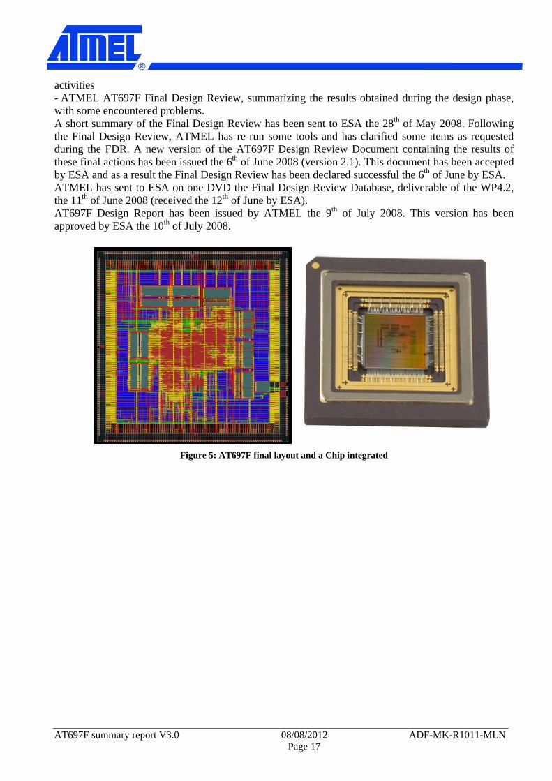
Figure 5: AT697F final layout and a Chip integrated
AT697F summary report V3.0 08/08/2012 ADF-MK-R1011-MLN Page 17
®
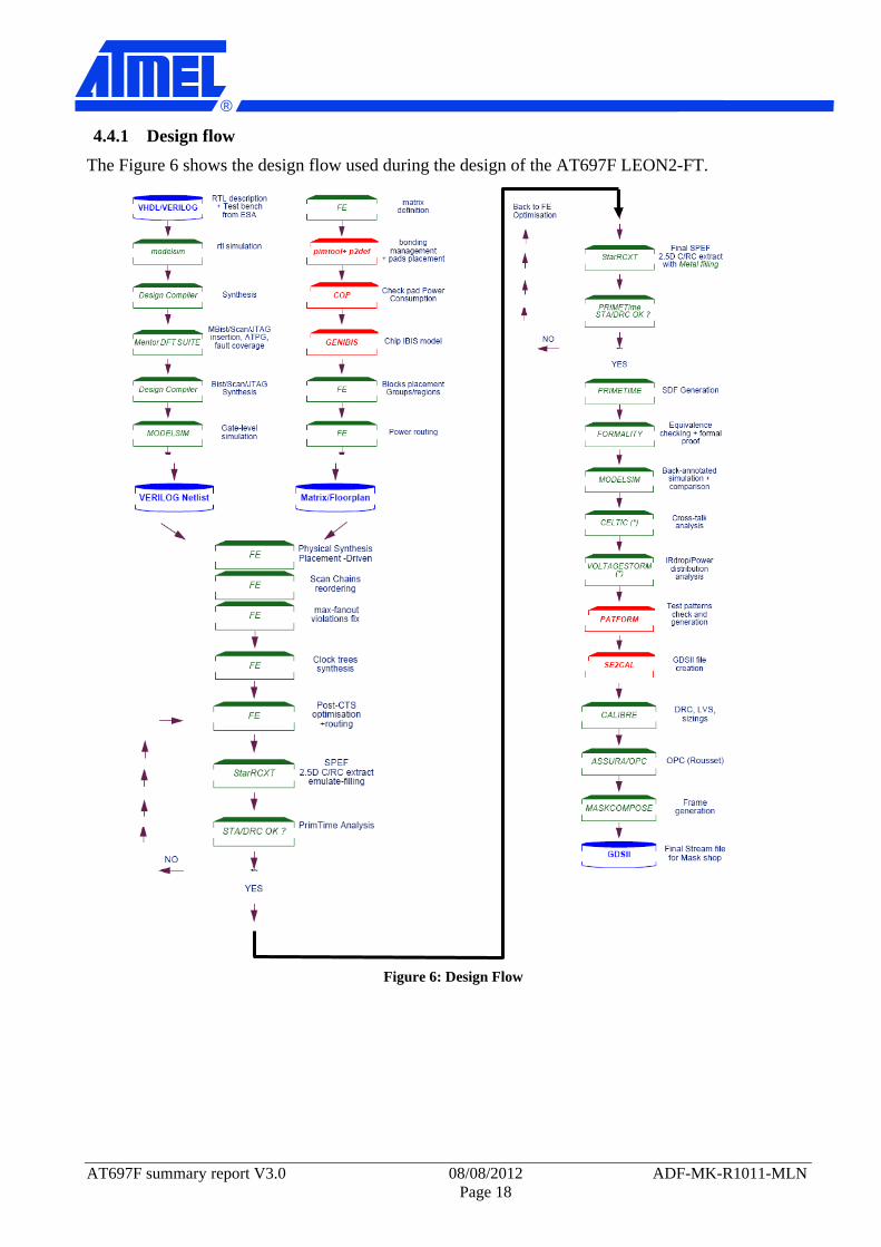
4.4.1 Design flow The Figure 6 shows the design flow used during the design of the AT697F LEON2-FT.
Figure 6: Design Flow
AT697F summary report V3.0 08/08/2012 ADF-MK-R1011-MLN Page 18

®
AT697F summary report V3.0 08/08/2012 ADF-MK-R1011-MLN Page 19
4.4.2 Main results 4.4.2 Main results The final place and route has given the chip view shown in the Figure 7 below, in an 8.6 x 8.6 mm matrix: The final place and route has given the chip view shown in the
Legend for ATF697E
Figure 7 below, in an 8.6 x 8.6 mm matrix:
Legend for ATF697E
Figure 7: AT697F (above) and AT697E (below) floorplans
JTA
PI
PIO C DA
AD
InsCac
PL
Trac
MEM IF
DS
SDRAM IF
PCI Req&gnt PCI
PC
JTAG
PIO
CB Data Cache DATA
ADD
InsCache
RegFile
PLL
Trace buffer
DSU
PCI
Legend for AT697F
Red : IU Pink : FPU Blue : caches Violet : amod Green : PCI Orange : DSU White : mctrl Dark blue : BIST Yellow : JTAG
IU-FPU-caches A
DSU JTAG
MBAPCI

®
4.4.3 Lessons learnt The design of the AT697F has been performed during 14 months, from mid March 2007 to mid May 2008. Even if the experience of the AT697E LEON2-FT prototype was useful and eased some AT697F design tasks, a number of difficulties due to the complexity of the design implied a significant delay, including : - Simulation debugging, - Artificial clock skew implementation, - External timing improvements. The performances obtained at the end of the AT697F design phase are promising and fully in line with the initial objectives of the ESA contract 19083/05/NL/FM: - The AT697F processor clock speed has been maintained at 100 MHz whereas the library maximum temperature is 145°C and not 100°C as it was for AT697E. - The artificial clock skew implementation and the hold margin have been improved. - The external interfaces speed has been significantly improved, allowing to get a fully 100 MHz processor on SDRAM or SRAM interfaces. A good collaboration with ESA has been noted all along the design phase, with an important number of design follow-up conference calls and two technical support visits of agency member at ATMEL premises. The 6th of June 2008, ESA has authorized ATMEL to proceed with the manufacturing of the AT697F processor.
AT697F summary report V3.0 08/08/2012 ADF-MK-R1011-MLN Page 20

®
5 Phase 4 5 Phase 4 5.1 WP 5: Detailed Test Plans 5.1 WP 5: Detailed Test Plans 5.1.1 Summary of the activities 5.1.1 Summary of the activities
After ESA authorisation to preceed, after the acceptance of the work package 3 and 4, the main task of the work package 5 was to produce all documents describing the detailed test plans. After several review the final documents were sent to agencies.
After ESA authorisation to preceed, after the acceptance of the work package 3 and 4, the main task of the work package 5 was to produce all documents describing the detailed test plans. After several review the final documents were sent to agencies. Electrical characterization test plan [25] Electrical characterization test plan D18-AT697F-ElectricalCharacterisationTestPlan-V2.0-2010-11-24 D18-AT697F-ElectricalCharacterisationTestPlan-V2.0-2010-11-24
[25]
Validation Test Plan [26] Validation Test Plan D19-AT697F-ValidationTestPlan-v1.1 D19-AT697F-ValidationTestPlan-v1.1
[26]
Contractor Internal Space Qualification test plan [27] Contractor Internal Space Qualification test plan D20-AT697F-ContractorInternalSpaceQualificationTestPlan-v1.1-2010-11-30 D20-AT697F-ContractorInternalSpaceQualificationTestPlan-v1.1-2010-11-30
[27]
Preliminary Radiation test plan [28] and [29] Preliminary Radiation test plan D21a-AT697F-TotalDoseTestPlan-v1.0-2008-09-26 D21a-AT697F-TotalDoseTestPlan-v1.0-2008-09-26
[28] and [29]
D21b-AT697F-SEETestDocuments-v1.2-2010-12-09 D21b-AT697F-SEETestDocuments-v1.2-2010-12-09 Preliminary Evaluation test plan [30] Preliminary Evaluation test plan D22-AT697F-EvaluationTestPlan-v1.2-2010-10-22 D22-AT697F-EvaluationTestPlan-v1.2-2010-10-22
[30]
5.2 WP 6: Manufacturing and Assembly of Engineering Devices 5.2 WP 6: Manufacturing and Assembly of Engineering Devices 5.2.1 Summary of the activities 5.2.1 Summary of the activities
Following the ESA authorisation to proceed, the manufacturing of the reticles has been launched in 2008w24, followed by the start of the lot fabrication itself. The lot was out of the fab 2008W36 and after the grinding process received at Nantes end 2008w37. The probe test started a week later 2008w38.
Following the ESA authorisation to proceed, the manufacturing of the reticles has been launched in 2008w24, followed by the start of the lot fabrication itself. The lot was out of the fab 2008W36 and after the grinding process received at Nantes end 2008w37. The probe test started a week later 2008w38. All probe test patterns passed successfully, and are used on all wafers before assembly. 30 part of AT697F engineering models in MCGA349 have been received beginning 2008w43 and 10 part AT697F engineering models in MQFPF256 have been received.
All probe test patterns passed successfully, and are used on all wafers before assembly. 30 part of AT697F engineering models in MCGA349 have been received beginning 2008w43 and 10 part AT697F engineering models in MQFPF256 have been received. For electrical characterisation and validation test one new wafer will be sent to assembly 2008w48. For electrical characterisation and validation test one new wafer will be sent to assembly 2008w48. A validation test board description has been sent to the agency 2008w45. ESA has reviewed the document, and ATMEL pursuit to the manufacturing of two test boards. A validation test board description has been sent to the agency 2008w45. ESA has reviewed the document, and ATMEL pursuit to the manufacturing of two test boards. 5.2.2 Main results 5.2.2 Main results
The AT697F has been assembled in two different package one 349-pin MCGA and in one 256-pin MQFP. Some slight timing discrepancies have been found but without any impact on the final specification, these differences have been reported in [32] as well as in the DLA_SMD [37].
The AT697F has been assembled in two different package one 349-pin MCGA and in one 256-pin MQFP. Some slight timing discrepancies have been found but without any impact on the final specification, these differences have been reported in [32] as well as in the DLA_SMD [37].
Figure 8: ATMEL AT697F package parts Figure 8: ATMEL AT697F package parts
25 mm
AT697F summary report V3.0 08/08/2012 ADF-MK-R1011-MLN Page 21

®
A validation test board including one mezzanine with an AT697F packaged in a MCGA 349 embedded in an Ironwood socket and one mezzanine with an AT697F packaged in a MPFQ256, have been sent to ESA in December 2010.
A validation test board including one mezzanine with an AT697F packaged in a MCGA 349 embedded in an Ironwood socket and one mezzanine with an AT697F packaged in a MPFQ256, have been sent to ESA in December 2010. This application board is shown in the Figure 9 and Figure 10. It implements ten AT60142F 4 Mbits SRAM developed under a CNES contract it can be seen with the MCGA and MQFP mezzanine. The user manual of the ATMEL evaluation board can be found on Atmel Web site. This board is commercialised by ATMEL as a development kit.
This application board is shown in the
Figure 9 and Figure 10. It implements ten AT60142F 4 Mbits SRAM developed under a CNES contract it can be seen with the MCGA and MQFP mezzanine. The user manual of the ATMEL evaluation board can be found on Atmel Web site. This board is commercialised by ATMEL as a development kit.
Figure 9: ATMEL AT697F evaluation board with MQFP256 mezzanine Figure 9: ATMEL AT697F evaluation board with MQFP256 mezzanine
Figure 10: ATMEL AT697F evaluation board with MCGA349 mezzanine
AT697F summary report V3.0 08/08/2012 ADF-MK-R1011-MLN Page 22

®
5.3 WP 7: Electrical Characterisation and Validation 5.3.1 Summary of the activities
The validation test plan [26] has been delivered and accepted by the agencies in December 2010. This document presents the validation strategy used by ATMEL to validate the AT697F processor. The AT697F validation consists of two validation processes. The first one uses industrial test equipment (ASIC tester) to characterise the processor, while the second one uses application laboratory equipment to perform functional validation and benchmarking.
5.3.1.1 Electrical characterisation
The electrical characterisation report [32] presents the detailed activities and results obtained during the characterisation of the AT697F using the Credence Octet tester, The Octet 800 has been used for the characterisation and the debugging, and then all the test patterns have been reworked to be ported on an Octet 200. The portability has been more complex than expected which has delayed the overall characterisations. Functional test patterns coming from the ESA test benches have been passed on the tester to validate the product functionality. Some additional patterns have been added by ATMEL to improve the validation such as new test-benches to test the Debug Support Unit (DSU), stuck-at faults and transition delay faults (TDF), Memory-BIST, JTAG, PLL, SRAM interface to improve the timings characterization. The AT697F characterisation has been performed on the military temperature range [-55°C; + 125°C] and for the whole bias range: (1.65V; 1.95V) for the core, (3V; 3.6V) for I/Os. The static parameters (current consumptions, input leakages, output currents) and dynamic parameters (setup / hold / output delay) have been measured in the above conditions.
5.3.1.2 Application validation
The validation report [34] presents the detailed activities and results obtained during the characterisation of the AT697F. Manpower restrictions have added delay to work package. 5.3.2 Main results
5.3.2.1 Electrical characterisation
The AT697F characterisation done in both package (MCGA and MQFP) has been performed successfully in accordance with the characterisation test plan [25]. The 10 MCGA349 & 2 MQFPF 256 package parts tested are fully functional in the whole bias and temperature range [-55°C; +125°C]. Static parameters are in line with the datasheet for example the following table gives the standby Array and Buffer Current consumption.
AT697F summary report V3.0 08/08/2012 ADF-MK-R1011-MLN Page 23

®
PARAM Type Spec. Average Sigma Min Value Max value Unit
ICCSB_Array Max 5 0.993 0.103 0.858 1.12 mA
ICCSB_ Buffer Max 5 1.18 0.873 1.04 1.27 mA
The maximum value measured is less than 1.5mA for both Array and Buffer for a specification at 5mA. The AC characterisation tests have been performed on the two different packages and with Natural and Maximum Skew. The dynamic parameters are in line with the Static Timing Analysis (for a typical lot). Only a very small number of minor deviations were noticed. All the values have been updated in the datasheet [35]. The final electrical characterisation report [32] has been sent to agencies end of November 2010. In conclusion, static and dynamic parameters measured on the chip are in line with the data sheet.
5.3.2.2 Application validation
For the validation a logic analyzer was used to acquire the chronograms and clock for the AT697F processor was injected by a generator with (3.3 V of amplitude and variable frequency). The DSU interface was used to program the AT697F processor. All internal modules have been tested with different test-benches and configurations. The bypass configuration switch was used for tests to frequency up to 80 MHz and for higher frequencies the internal PLL was used. For example the FPU module was tested with specific benchmarks (paranoia, linpack and whetstone) with different configurations at different frequencies. A test performed at 40 MHz with the software option –MSFLOAT, WS3, cache ON, shows the performance of the FPU of the processor compare to the software FPU. • The result of this test is 2.9 Paranoia/second with software FPU. • The result of this test is 75.8 Paranoia/second with hardware FPU. The ratio between the hardware FPU and the software FPU is around: 26. All regfile with and without EDAC protection, Instruction and data caches, interrupts and trap, memories (ROM, SRAM and SDRAM), UART tests have passed successfully. The PCI validation has been done by Atmel, and not any more by Ayrton (as for AT697E PCI validation) subcontractor. Atmel does have all necessary software and hardware to perform the tests. Power consumption was monitored and characterized under different application and at different CPU clock frequencies. Performance Summery: (at 100MHz, SRAM with 2 wait-states) 85 MIPs (Dhrystone 2.1), 76DMIPS Whetstone Double precision 22.3 MWIPS, 7 MFLOPS Whetstone Single precision: 27.4 MWIPS, 10.2 MFLOPS Functional Validation Summary BUG1: Odd-numbered FPU register dependency (known since tape-out) No new bug found by validation The Applicative validation report [34] has been sent to agencies end of March 2012.
AT697F summary report V3.0 08/08/2012 ADF-MK-R1011-MLN Page 24

®
5.4 WP 8: Contractor Internal Space Qualification
The main activity of this work package was to define and perform the qualification tests (Characterization, electrical test, Probe test, Assembly, Final test, Electrical characterization, ESD, Latch up) and Reliability tests: Die qualification test (early failure rate 150°C/3.7v, operating life test 150°C/3.7v, Static Life Test 140°c, Endurance 25°c , Data-Retention Wafer Level 250°C, Data-Retention Product Level 150°C) and the Package qualification tests. The Contractor Internal Space Qualification test Plan [27] has been sent to ESA in November 2010.
The main results are presented with the WP10.
5.5 WP 9: Radiation Characterisation 5.5.1 Summary of the activities
This work package 9 is executed under CNES contract N° 721/00/8286/02. The preliminary radiation test plans have been sent according to the work package 5. The documents AT697F total dose test plan [28] has been reviewed by ESA and CNES, and has been accepted. The Total ionizing dose has been performed from the 18th of November 2008 and the 5th of January 2009. The AT697F total dose test report [38] document has been sent 2009w7 and reviewed by Agencies. The TID test last from November 2008 to 2009w2. The document AT697F SEE test plan [29] has been sent to and reviewed by agencies. A new heavy ion test platform has been developed to the SEE tests. This platform is made of three boards, the main board which embeds all useful components to activate the DUT and to perform all tests software. Two other boards (mezzanine), one for each type of package MCGA and MQFP, used for heavy ion when attached to the main board and used for protons testing attached through 2 meters cable to main board, to allow the main board to be far enough from the proton beam. Three SEE test campaigns have been done, two heavy Ion campaigns And one Protons campaign. - Heavy Ion Campaign on 8th of September 2010, at HIF UCL - Heavy Ion Campaign on 20th of November 2010, at HIF UCL - Protons Campaign on 29th of September 2010, at LIF UCL 5.5.2 Main results
The main board and a mezzanine are shown below.
Figure 11: Assembled radiation test main board
AT697F summary report V3.0 08/08/2012 ADF-MK-R1011-MLN Page 25

®
Figure 12: AT697F MQFPF256 mezzanine board
The AT697F total ionising dose test report [38] and the AT697F Single Event Effects test report [39] present the detailed activities and results obtained during the radiation tests performed on the AT697F. The AT697F total ionizing dose (TID) tests have been performed in two campaigns: the first one was held on 10 parts from December to January 2009 up to 300 Krad (Si), and the second was held on 22 parts up to 300 Krad (Si). The parameters measured during the read-outs and after annealing were all the DC and AC parameters mentioned in the datasheet. The good results confirm the total ionizing dose radiation hardness shown on the ATC18RHA technology. Three heavy ions Single Event Effects (SEE) test campaigns for the AT697F have been performed at the Université Catholique de Louvain (UCL):
- Heavy Ion Campaign on 8th of September 2010, at HIF UCL - Heavy Ion Campaign on 20th of November 2010, at HIF UCL - Protons Campaign on 29th of September 2010, at LIF UCL These three SEE test campaigns have allowed to assess the Single Event Upsets / Single Event Transients sensitivity for the AT697F and to check the protection against Single Event Latchup. The set of functional patterns were enhanced to check the occurrence of SEFIs. Tests were composed of: - Static tests: memory elements are exhaustively SEU tested (Registers, Caches, DFF), protected or not. - Dynamic tests: The results of computation (subject to SEUs in memory elements and SET in the logical elements) with or without mitigation schemes are assessed. The SEL test has been performed at a temperature of 125°C, at maximum voltage and for a LET of 62 MeV/mg/cm2 there is no Single Event Latchup for AT697F for a fluence of 2 107 particles / cm2. The Latchup cross section can be estimated to be lower than 5 10-8 cm² The SEU tests show that the RHBD techniques applied in AT697F such as EDAC, parity, Triple Modular Redundancy (TMR) are working correctly. Only few MBU have been observed at high LET. The SEU low sensitivity is enhanced with good practises like cache occupancy management. During all the tests no functional disruption has been found.
AT697F summary report V3.0 08/08/2012 ADF-MK-R1011-MLN Page 26

®
The SET tests show that the TMR technique and the clock skew mechanism allow a very good filtering of the SET in the combinational and sequential logic. The proton test shows a very low sensitivity to energy of 63MeV. A good correlation has been established between the SEU test results obtained on the ATC18RHA 0.18µm family and the ones obtained on AT697F. The efficiency of the AT697F SEU and SET protections has been confirmed. The influence of the skew and frequency has been assessed, confirming that the maximum skew achieves a significant protection improvement against SEU and SET. During all the SEU runs that have been performed during these test campaigns, only a few residual, uncorrectable errors have been detected. The associated error rate in geostationary orbit has been determined to be better than 1 E-5 error/device/day, and it can be concluded that the AT697F, for space applications, is a SEU/SET hardened processor. 5.5.3 Lessons learnt
The first main board was inspected without any component in order to verify all the power lines, at that time it has been observed that the board was twisting and could not be used for the components assembly. The internal layer metal was incorrectly well-balanced. A new internal metal has been done and sent to the subcontractor in order to make a new main board. The new main board fully assembled and the two mezzanines released were fully operational. We have observed that the connector was not the expected one due to a mistake in the bill of material therefore the heat equipment could not be properly installed on the back side of the DUT. The subcontractor used for AT697E test campaign was unable to complete the software development and the test of the board. Therefore Atmel had decided to stop the subcontractor contract and handed the radiation testing activity over to iROC. iROC had restart the board test and debug. iROC had developed the software environment and the test which have been used during the heavy Ions and Protons test campaign. The SEE tests have also shown that a careful initialisation of the processor and handling of the SEU protection mechanism is required in boot and application software to prevent accumulation of single errors to cause uncorrectable multiple errors. This knowledge will need to be transferred to users in documentation, example code and technical support.
5.6 WP10: Evaluation 5.6.1 Summary of the activities
ATMEL has used the engineering lot for the electrical characterisation and validation and for the evaluation to be performed in WP10. For the ATMEL internal space qualification performed in WP6 however, the production lot has been used. This allowed ATMEL to assess the product variability to the process. All the tests performed are described in the Evaluation test plan [30]. All the parts were coming from 8S5247P silicon lot (date code 0942). All parts used for this evaluation have been previously tested by the production test area with the following flow: - Electrical measurements at room temperature (+25°C) - Electrical measurements at low temperature (-55°C)
AT697F summary report V3.0 08/08/2012 ADF-MK-R1011-MLN Page 27

®
- Electrical measurements at high temperature (125°C) - External visual inspection - Dimension check - Solder ability - Resistance to solvents - Terminal strength - Bond strength - Stud pull test 5.6.2 Main results
The assembled parts have been tested to: - The CDM and HBM ESD. to estimate the susceptibility to damage and degradation by exposure to electrostatic discharge. Parts passed the 2000V level without any damage on I/O 3.3v. According to the CDM results the product is classified in Class 4 of the ESD association. - The Electrical latch up. All parts tested show no sensibility to power injection at 25°C and at 125°C - The Breakdown voltage. The break down voltage test is used to test functionality after voltage or current stress. All parts tested show no sensibility. - Electrical characterization (Verification of functionality over an extended voltage range). All Functional test patterns have been successfully passed in military temperature range. Static and Dynamic parameters have been measured and correlated with the simulation results. - Construction Analysis. Detailed results are reported in CNES Precap Report_8S5247P-2_07-10-09 - SEM inspection – micro sectioning with glassivation layer integrity. Detailed results are reported in document SL209-8967. - Bond strength and substrate attach strength (stud pull test). Detailed results are reported in the CNES Electrical Acceptance. - Thermal Tests. The purpose of these tests is to evaluate the behavior of the product subject to thermal constraints. 10 parts have been tested and no weakness to thermal constraints has been identified. - Mechanical Tests. The purpose of these tests is to evaluate the behavior of the product subject to mechanical constraints. 10 parts have been tested and no weakness to mechanical constraints has been identified. - Endurance tests. 1000h Read Out done successfully and internal Atmel qualification done. ESCC qualification (3000h) and all groups are done. A final report has been sent to agency [43].
AT697F summary report V3.0 08/08/2012 ADF-MK-R1011-MLN Page 28

®
6 Deliverables Fifteen AT697F parts have been delivered to ESA during the Phase 4, WP7 and WP8, from December 2008 to November 2011. An AT697F Validation test board including the Board, a MCGA mezzanine (with socket) and a MQFP mezzanine has been delivered to ESA in November 2010. All the following documents (except the customer oriented ones) written by ATMEL are ATMEL Proprietary and, as such, confidential. These documents are included in the final CD-ROM delivered to ESTEC at the end of this Phase 4.
6.1 Design related documents D13-AT697F-DesignReviewDocument-v2.1-2008-06-06 – ADF-DE-R0612-MLN V2.1 D14-AT697F-DesignReport-v2.0-2008-07-03 – ADF-DE-R0611-MLN V2.0 D15-AT697F-TimingDatabook-v1.1-2008-04-30 – ADF-DE-R0603-MLN V1.1 D16-AT697F-SRAMTimingAnalysis-v2.0-2008-03-31 – ADF-DE-R0600-MLN V2.0 D16-AT697F-SDRAMTimingAnalysis-v2.0-2008-03-31 – ADF-DE-R0601-MLN V2.0 D16-AT697F-PCITimingAnalysis-V1.0-2008-03-03 – ADF-DE-R0602-MLN V1.0 D16-AT697F-SkewAndHoldAnalysis-V1.0-2008-03-31 – ADF-DE-R0604-MLN V1.0
6.2 Customer oriented documents D17-AT697F-PreliminaryDatasheet-revC-2009-06-30 – 7703C-AERO D26-AT697F-UpdatedDataSheet-RevE-2011-08-04 – 7703E-AERO Preliminary SMD Specification – 5962-07224 Rev C AT697F_erratasheet_draft2 AT697F Total ionizing Dose test report – mtr110407 L2.6-AT697F-ESCCSpecification-V1.1-2011-10-24 – ESCC Spec. No. 9512
6.3 Validation and Characterisation related documents D18-AT697F-ElectricalCharacterisationTestPlan-V2.0-2010-11-24 – ADF-PE-R0821-MLN V2.0 D19-AT697F-ValidationTestPlan-v1.1-2010-12-10 – ADF-DE-R0940-MLN V1.1 D20-AT697F-ContractorInternalSpaceQualificationTestPlan-v1.1-2010-11-30 – ADF-PE-R0822-MLN V1.0 D22-AT697F-EvaluationTestPlan-v1.2-2010-10-22 – ADF-PL-R0972-MLN V1.2 D23-AT697F-ValidationTestBoard-v1.4-2011-10-24 – 7740D-AERO V1.4 D24a-AT697F-ElectricalCharacterisationTestReport-v5.1-2010-11-25 – ADF-PE-R0834-MLN V5.1 D24b-AT697F-T14-T17-Report-v2.1-2010-11-25 – ADF-PE-R0840-MIL V2.1 D25-AT697F-ValidationTestReport-v1.2-2012-03-29 – ADF-DE-R0941-MLN V1.2
6.4 Radiation related documents D21a-AT697F-TotalDoseTestPlan-v1.0-2008-09-26 – ADF-PL-R0970-MLN V1.0 D21b-AT697F-SEETestDocuments-v1.2-2010-12-09 – ADF-PL-R1007-MLN V1.2 L1.2a-AT697F-TotalDoseTestReport-v2.0-2009-11-16 – ADF-PE-R0835-MLN V2.0 L1.2b-AT697F-SEETestReport-v2.2-2011-12-06 – ADF-PE-R0842-MLN V2.2 L2.1-AT697F-SEETestProgramSoftware-v1.0-2010-12-16.zip
6.5 Qualification related documents L2.2-CNES Precap Report_ 8S5247P-2_ 07-10-09 L2.3-CNES Electrical Acceptance L2.5 -AT697F- EvaluationReport-v1.4-2012-03-07 – ADF-PE-R1001-MLN rev1.4 L2.6-AT697F-ESCCSpecification-V1.1-2011-10-24 – ESCC Spec. No. 9512 L2.7-Process identification document PID – PID0030 Rev B
AT697F summary report V3.0 08/08/2012 ADF-MK-R1011-MLN Page 29
®
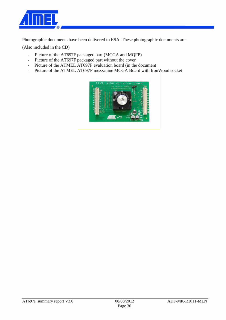
Photographic documents have been delivered to ESA. These photographic documents are:
(Also included in the CD)
- Picture of the AT697F packaged part (MCGA and MQFP) - Picture of the AT697F packaged part without the cover - Picture of the ATMEL AT697F evaluation board (in the document - Picture of the ATMEL AT697F mezzanine MCGA Board with IronWood socket
AT697F summary report V3.0 08/08/2012 ADF-MK-R1011-MLN Page 30

AT697F summary report V3.0 08/08/2012 ADF-MK-R1011-MLN Page 31
®
7 Conclusion The flight version of the LEON2-FT processor AT697F benefit from the experience gained during the development of the LEON2-FT prototype AT697E. The AT697F is based on the ATC18RHA library and correct all the bugs that were identified on the AT697E. The AT697F processor has been made available to the European space community since 2011. The Design phase has been performed from March 2007 to May 2008. Following the ESA authorisation to proceed, the manufacturing of the reticules has been launched in June 2008, engineering model packaged in MCGA and MQPF was made available for validation in October 2008. The validation, characterisation and radiation tests have been performed from January 2009 to March 2012, and the results are very positive:
- The AT697F is fully functional, only the bugs known at the end the design phase are present. - The performance of the processor reaches the specification, for a power consumption as low as
7 mW / MHz. - The AT697F fully works over the whole bias and military temperature ranges. - The AT697F has been tested successfully up to a total dose of 300 Krad(Si). - The AT697F is a SEU/SET hardened processor. The hardware TMR technique is very effective
against SEU in the internal sequential logic and SET in the combinational logic network, even at 100 MHz (PLL enabled) and with a natural Skew. There are very few errors that escape mitigation by this technique. There are not enough events to be able to evaluate the influence of the maximum Skew on the error rate.
- There is no Single Event Latchup (SEL) at 125°C for a LET of 62 MeV/mg/cm2 with maximum voltage levels on core (1.95V) and I/Os (3.6V).
These TID and SEE test results have confirmed the high tolerance of this product against radiation effects and its capability to answer to the needs of the space community.The feedbacks from the customers that have already used the chip (alpha customers, early design starters) are as well very positive. The space community in general shows a very good interest in the AT697F. ATMEL would like to thank the following ESA persons that have allowed carrying out this difficult but finally successful design of the AT697F microprocessor: - Andre L. R. Pouponnot (TEC-EDD), Technical Officer, - Roland Weigand (TEC-EDM) for his technical support.