ses. focused ion beam - ucla · 424 mrs bulletin • volume 32 • may 2007 •...
TRANSCRIPT
424 MRS BULLETIN • VOLUME 32 • MAY 2007 • www/mrs.org/bulletin
Fundamentals ofFocused Ion BeamNanostructuralProcessing: Below,At, and Above theSurface
Warren J. MoberlyChan, David P. Adams,Michael J. Aziz, Gerhard Hobler,
and Thomas Schenkel
structures in situ, and provide site-specificextractions for further ex situ processing oras sample preparation for other analy-ses.1–3 Ion beam processing predates FIB,ranging from processing films for semi-conductor devices to the preparation oftransmission electron microscopy (TEM)samples,4 and the ion/surface interactionhas been understood and optimized inone-dimensional processing at doses up toroughly 1015/cm2 (e.g., semiconductordoping). The FIB has extended the appli-cations to a regime in which localized,three-dimensional (3D) ion/surface inter-actions are important, with doses of~1018/cm2 and unprecedented currentdensities. The FIB as a processing oranalysis tool has commonly used a fixedaccelerating voltage and ion species (30keV Ga); however, multispecies ionsources with variable voltage (<1 kV to>50 kV) are promising.5 New FIB toolcapabilities are being developed to meetmore stringent requirements, such as TEMsample preparation with reduced surfacedamage and shallower implants driven byfurther miniaturizations of microelec-tronic devices. Traditionally, the ion/sur-face interaction caused a damage zonethat often had to be subsequentlyremoved by chemical etching or annealingprocesses. A damage zone of a fewnanometers, whether implanted below orredeposited above the surface, often canbe tolerated for microdevices but not fornanodevices. With 3D site specificity in anFIB, that which was termed “damage” or“artifact” may be controlled, understood,and even utilized for nanostructures.
As FIBs evolve from processingmicrodevices to nanodevices, some differ-ences arise. FIB micromachining hasbecome a broad field of its own,6 anda future field of FIB nanomachiningneeds further development. Computer-controlled micromachining presupposesthat the tool operates at a constant etchrate. For FIB machining at the nanometerscale, however, sputter yields may nolonger be considered constants. The pres-ent-day FIB offers a range of currents andbeam sizes, with a common smallest beamof 4–6 nm. Future FIB nanomachiningmay need a smaller spot; however, anenergy reduction will be required to limitthe present beam spread of 4–20 nm insidethe sample (e.g., Figure 1). Furthermore, atthe micron scale, the initial damage doneby the FIB during setup of the process canbe ignored, enabling quick FIB imagingand beam shifts (and/or computerimage recognition) to be performed withimpunity. However, at the nanometerscale, such FIB setup damage cannot betolerated. This will require more reliable
AbstractThis article considers the fundamentals of what happens in a solid when it is
impacted by a medium-energy gallium ion. The study of the ion/sample interaction atthe nanometer scale is applicable to most focused ion beam (FIB)–based work even ifthe FIB/sample interaction is only a step in the process, for example, micromachining ormicroelectronics device processing. Whereas the objective in other articles in this issueis to use the FIB tool to characterize a material or to machine a device or transmissionelectron microscopy sample, the goal of the FIB in this article is to have the FIB/sampleinteraction itself become the product. To that end, the FIB/sample interaction isconsidered in three categories according to geometry: below, at, and above the surface.First, the FIB ions can penetrate the top atom layer(s) and interact below the surface.Ion implantation and ion damage on flat surfaces have been comprehensivelyexamined; however, FIB applications require the further investigation of high doses inthree-dimensional profiles. Second, the ions can interact at the surface, where amorphological instability can lead to ripples and surface self-organization, which candepend on boundary conditions for site-specific and compound FIB processing. Third,the FIB may interact above the surface (and/or produce secondary particles thatinteract above the surface). Such ion beam–assisted deposition, FIB–CVD (chemicalvapor deposition), offers an elaborate complexity in three dimensions with an FIB usinga gas injection system. At the nanometer scale, these three regimes—below, at, andabove the surface—can require an interdependent understanding to be judiciouslycontrolled by the FIB.
IntroductionThe focused ion beam (FIB) is becoming
an ideal tool for growing, sculpting, infus-ing, and observing small shapes in anever-widening range of applications. Inconjunction with scanning electron
microscopy (SEM) as well as an increasingvariety of add-on tools (micromanipula-tors, gas-injection systems, and spectro-scopic and crystallographic analysis), theFIB can prototype devices, characterize
MRSBull_May07_Moberly_Final.qxd 5/7/07 6:19 PM Page 424
Fundamentals of Focused Ion Beam Nanostructural Processing
MRS BULLETIN • VOLUME 32 • MAY 2007 • www/mrs.org/bulletin 425
concentric dual-beam systems, with theSEM or other technologies (e.g., Figure 2)providing precise site-specific setup forFIB nanostructuring. Developing FIBs willovercome many present-day engineeringhurdles, yet the physics of the ion/surfaceinteraction will remain essentially thesame. Although larger structures of thepast have compelled individual study ofinteractions only below, at, or above sur-faces, future small 3D structures willrequire a more comprehensive, interde-pendent understanding of all three.
FIBs Below the Surface: Local 3DImplantation and Single Dopants
When an energetic ion enters a surface,several effects occur, including implanta-tion, damage, mixing, electron emission,and chemical reactions, in addition tosputtering. These physical phenomena aresimilar for FIBs or broad static beams(reviewed earlier);4 however, lateral con-finement differences arise when FIB per-
forms direct-write of nanometer-scalestructures.
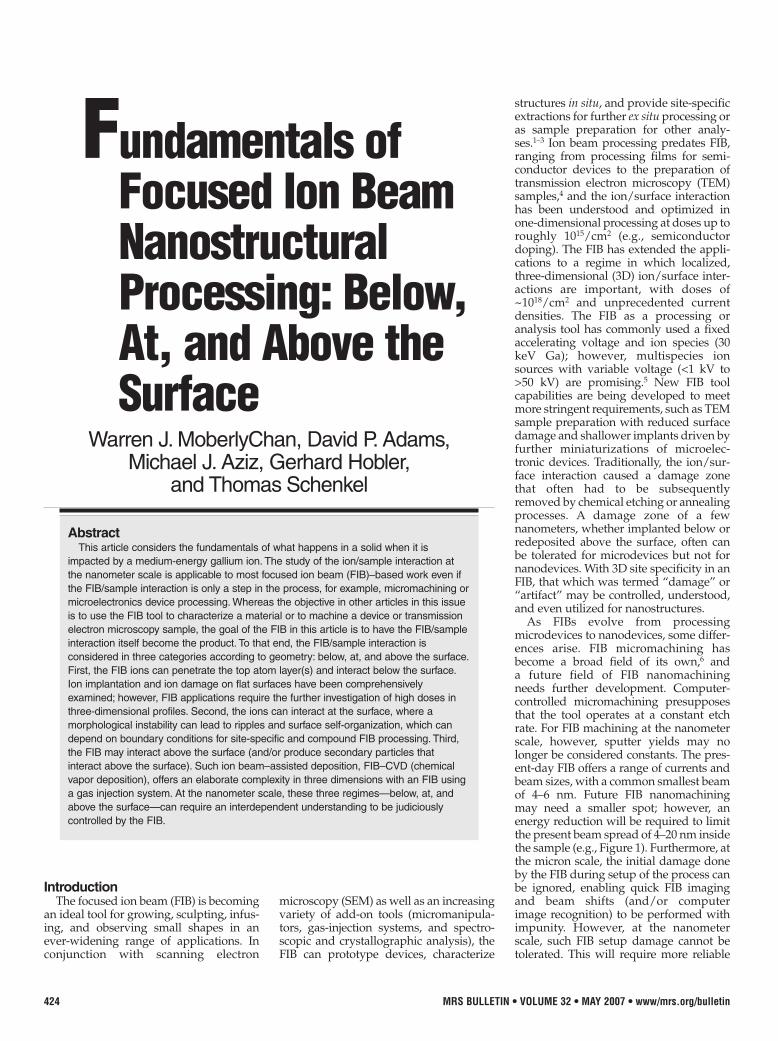
The minimum feature size is deter-mined by beam width, ~4–10 nm in state-of-the-art FIBs. The spread of the collisioncascade (Figure 1a) does not influencesputtering as long as the beam is normalto the surface. Monte Carlo simulations ofthese conditions (Figure 1b) show thatmost sputtered atoms originate from a1 nm3 volume around the impact point.7In contrast, beam effects below the surfacehave a wider lateral spread. For example,the full width at half maximum (FWHM)of the lateral dopant distribution causedby a zero-width 30 keV Ga+ beam in Si is20 nm.
Ion effects below the surface are sometimes intended (e.g., doping) andsometimes unintended (e.g., samplesmade amorphous during FIB prepara-tion). In both cases, it is desirable to esti-mate the range as the sum of the projectedrange, Rp, plus several standard devia-tions, sp, of the implant profile Rp + nsp,where n is an integer and Rp and sp areeasily calculated by SRIM (a program forcalculating the stopping range of ions inmatter).7 Monte Carlo TRIM (transportrange of ions in matter) simulates moreaccurate estimates of the dopant and dis-placed atom (vacancy) distributions for aflat surface, f(x), assuming unit dopantdose and neglecting sputtering and theincorporation of the beam atoms into thesurface. The effect of surface movementcan be accounted for, while neglecting thevolume of the implanted atoms andatomic mixing.8 This leads to an expres-sion for the atomic density N(x) of theimplanted or displaced atoms valid fordilute concentrations, where x is a variableinvolving spatial dimensions, and x ¢ indi-cates a moving version of that variable:
(1)
N0 denotes the atomic density of the tar-get, Y the sputtering yield (which mayalso be estimated by TRIM), and d thethickness of the sputtered layer. In thesteady-state limit d Æ ∞, Equation 1 hasbeen used to estimate the depth at whichthe Ga or displaced atom concentrationdrops to 1018 cm-3 for a Si target bom-barded with a Ga beam at normal inci-dence (Figure 1a). Also, Equation 1 mayestimate the depth of the amorphous layerusing a critical displaced atom density of1022 cm-3 for the crystalline to amorphoustransition in Si.9 Although Equation1 becomes invalid for high concentrations,it qualitatively shows that the doping den-sity decreases with increasing sputtering
yield. Thus for glancing angles, such as inTEM lamella preparation, the sputteringyield is increased and doping can be min-imized. In contrast, when the effectivesputtering yield is decreased by redeposi-tion, such as at the bottom of a trench, thedoping and damage levels are increased.
A doping density approaching the tar-get density can only be treated bydynamic Monte Carlo simulations, which
f (x′)dx′.N(x)x+d
x
N0
Y= ∫
Figure 1. (a) Range of Ga and damageprofiles in Si at different concentrationlevels. (b) Sputtering yields of Sibombarded with Ga as a function ofenergy as calculated by TRIM(neglecting the implanted Ga ions) andby TRIDYN (after a steady-stateimplantation profile has developed).The star corresponds to anexperimental result.12
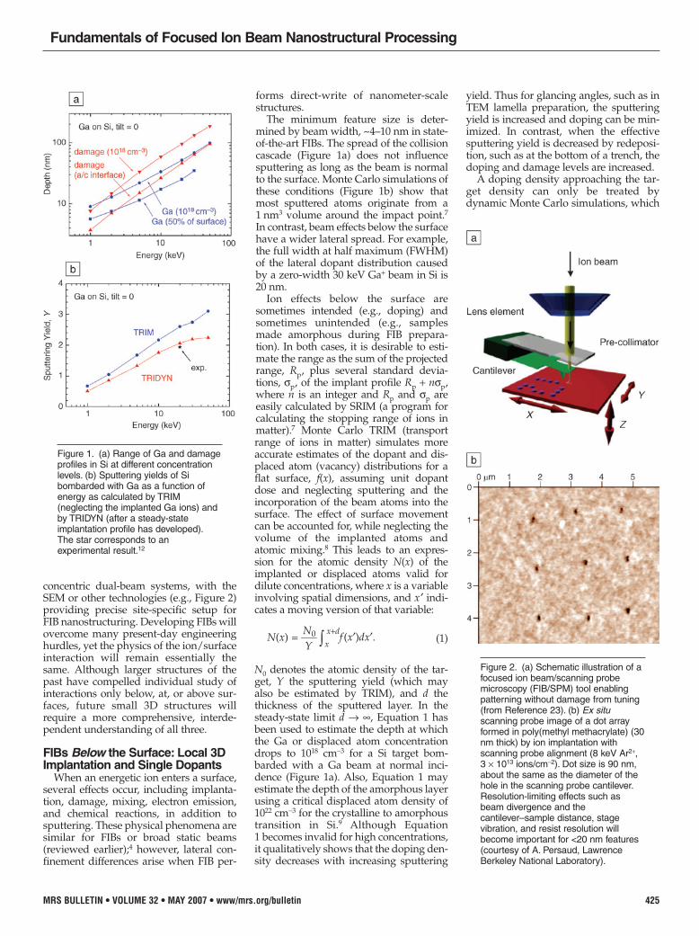
Figure 2. (a) Schematic illustration of afocused ion beam/scanning probemicroscopy (FIB/SPM) tool enablingpatterning without damage from tuning(from Reference 23). (b) Ex situscanning probe image of a dot arrayformed in poly(methyl methacrylate) (30nm thick) by ion implantation withscanning probe alignment (8 keV Ar2+,3 ¥ 1013 ions/cm-2). Dot size is 90 nm,about the same as the diameter of thehole in the scanning probe cantilever.Resolution-limiting effects such asbeam divergence and thecantilever–sample distance, stagevibration, and resist resolution willbecome important for <20 nm features(courtesy of A. Persaud, LawrenceBerkeley National Laboratory).
MRSBull_May07_Moberly_Final.qxd 5/7/07 6:19 PM Page 425
consider the implanted ions as possibletargets and takes their volume intoaccount. The TRIDYN program (based onTRIM code)10 calculates the positionwhere the Ga density drops to 50% of itssurface density for Ga implanted into Si(Figure 1a). For conventional FIB energies,the Ga doping is almost completely withinthe amorphous damage layer. However,at low energies, the highly doped Garegion extends beyond the amorphousdepth. Thus, low-keV polishing of Si TEMlamellae2,11 will still produce a thin Ga-rich layer as contamination even thoughnegligible amorphous Si remains on thesurfaces. Correct predictions of the surfacedensities are also essential to determinethe correct sputtering yields because thebeam and target atoms likely have differ-ent yields. Figure 1b shows a comparisonof Si sputtering yields obtained by TRIMand TRIDYN, using default parameters inboth cases. The TRIDYN results matchrecent experimental results.12
The dopant and damage ranges, as wellas the sputtering yield, are changed underchanneling conditions, where nuclearstopping is largely reduced. Channelingprimarily occurs when the beam isaligned with a low-index crystallographicaxis or plane and when the target is notmade amorphous (such as pure metals).For most FIB ion species and energies andmost targets, nuclear stopping dominatesover electronic stopping. Thus, sputteringis reduced, and the ion range is consider-ably increased under channeling condi-tions.4 Surprisingly, channeling may alsoplay a role in targets becoming amor-phous.13 General-purpose simulationtools are now being developed to predictthe exact 2D or 3D topography that formsunder FIB irradiation.14–16 Such tools arenecessary in an iterative procedure todetermine FIB parameters to obtain adesired nanosculpture.12
An ultimate goal of FIB is to process sin-gle dopant atoms using lower beam cur-rents, faster computer control, and futuredesign alternatives for alignment (tuning)and in situ metrology. Single defects andsingle dopant atoms can significantly alterthe performance of electronic devices suchas field-effect transistors, even at roomtemperature, for devices 10 nm in size. Thecorresponding variability of device per-formance because of discrete dopant dis-tributions is a potential scaling barrier.17,18
Single defects (even ones induced by cos-mic radiation) can also significantly alterthe performance of devices or lead to sin-gle-event upsets in memory cells, andunderstanding the effect of single-ionimpacts on devices is important toimprove radiation hardness. A comple-
mentary view considers classes of deviceswhere functionality is based on the pres-ence and precise manipulation of singledopant atom states. Coherent manipula-tion of spin states of phosphorus or anti-mony atoms in a silicon matrix has beenenvisioned as a path to scalable quantumcomputing.19–21
FIB doping of nanometer-scale deviceswas explored with tools available in the1980s.1,22 Besides throughput, several limi-tations persist for conventional FIB tools asprecision ion implanters. Dopant speciesand implant energies are not easily variedin one tool, dose control is difficult, andmost systems are not equipped with amass analyzer. The development of high-brightness sources capable of producingions of different species can ease the firstrestriction.5 Achieving small spot sizeswith variable beam energies has beendifficult with traditional focusing columns.Finally, the ion beam must not imagethe region of interest during tune-upalignment, as this introduces an unwanteddopant dose. The latter requirementnecessitates superb alignment of the ionbeam with an electron beam (e.g., indual-beam systems) and/or a high-preci-sion stage for displacement of the samplefrom the tuning area into the region ofinterest.
The ideal precision implanter may even-tually be able to deliver defined numbersof ions from elements with a range ofkinetic energies from across the periodictable into precise locations in a device.Fabrication of a Kane-type quantum com-puter calls for placement of individualGroup-V dopants into Si with a spacing of20–30 nm and accuracy of a few nanome-ters. Radiation-induced single defects canalter transistor performance in sub-100-nm gate length devices, and testing theseradiation effects requires reliable place-ment of ions into device channels. Factorscontributing to placement accuracy are theeffective beam spot size, range stragglingcaused by statistical energy loss processes,and diffusion during post-implant activa-tion annealing. The last is sensitive todefect injection from the dielectric–siliconinterface for specific dopants, which leadsto enhancement of diffusion for phospho-rus and retardation of diffusion for anti-mony in the presence of an imperfectSiO2/Si interface. The highest placementaccuracy is achieved with low-energyheavy ions. For 30 keV Ga+ beams, place-ment of single ions can be expected withinthe achievable beam spot sizes of about 10nm. However, a low-intensity beam (~1pA) provides a weak secondary electronimage and still can induce damage duringtuning/alignment.
An alternative to beam tuning ina nearby sacrificial region is to performthe imaging function with a scanningprobe (Figure 2a). Here, the ion beam iscollimated and transported through asmall aperture; however, the sample isnoninvasively imaged by a scanning forcemicroscope (SFM) while the ion beam isoff. This recently developed tool usesa piezoresistive force readout for SFM.23
Holes are drilled into a silicon cantileverusing a standard FIB and thin-film deposi-tion. Holes with diameters as small as 5nm are formed by drilling a large hole firstand then reducing the hole diameter bydeposition of a thin Pt film.24 The collima-tor will deteriorate after extended beamexposure, but the dose for this can be esti-mated from the drilling conditions underwhich the aperture was formed in the firstplace. Also, perforated cantilevers can berefurbished after extended use (holes canbe reshaped and imaging tips can besharpened). Whereas a 5–10 nm imagingresolution is superb for FIB imaging, thismodest resolution can be achieved in anSFM without excessive vibration isolation.With collimators of 5–10 nm in diameter,the integration of FIBs with SFMsoffers a reliable route to precision dopingof nanodevices.
Figure 2b depicts a pattern formed inresist by ion implantation with scanningprobe alignment. To control processing,the detection of single-ion impacts can bemonitored via detection of secondary elec-trons through the pick-up of the chargepulse of electron–hole pairs that formwhen ions impinge on semiconductors.The former is very universal, but requiresa secondary electron yield of >1 forreliable single-ion detection. Secondaryelectron yields are material-specific butcan be enhanced by lowering the workfunctions (e.g., depositing a low coverageof cesium). The kinetic energy and thecharge state of the incident ions alsoaffect SE yields.25,26 The detection of ionbeam–induced charge (IBIC) can beadministered relatively noninvasively byelectrical connections to samples tens ofmicrons away from the region of interest.27
The ultimate limit in single-ion place-ment depends on the ion energy andspecies, the target material, and the aper-ture size in the collimator. Optimizedcollimators can provide an ultimate place-ment resolution of <5 nm for low-energyheavy ions.
FIBs At the Surface: MorphologyEvolution during Erosion
A starting surface is traditionally 2Dflat, and yet FIB produces 3D struc-tures with variable slopes and nanometer
Fundamentals of Focused Ion Beam Nanostructural Processing
426 MRS BULLETIN • VOLUME 32 • MAY 2007 • www/mrs.org/bulletin
MRSBull_May07_Moberly_Final.qxd 5/7/07 6:19 PM Page 426
tolerances that require improved under-standing of 3D physics.
Three FIB issues can affect surfacetopography: machining, lithographic pat-terning, and the ion/surface interaction.First, as an engineering cutting tool,micromachining is becoming nanoma-chining, with correspondingly tighter tol-erances. Second, the superior resolution ofan FIB compared with photolithographyinvites its use for specialty direct-writepatterning with ever-higher aspect ratios.Third, the ion–surface interaction physicsdepends on local slope and curvature;hence, the evolving 3D morphology at thenanometer scale is not fully predictable.At the micron scale, the machining orpatterning capabilities of an FIB may beindependently engineered.6 Above themillimeter scale, the physics of broad-beam processing is a stand-alone science.4However, all three issues are colliding asFIBs process nanometer-scale shapes. Thissection compares the role of ion–surfacephysics on developing topography by FIBversus broad beam as well as the interac-tions among all three issues when fabricat-ing nanostructures.
FIB tools are designed to expedientlyion etch or machine surfaces, but suchsputter etching typically roughens sur-faces at submicron length scales. An idealFIB might machine away one atom layerwith neither disruption of the atoms in thenext layer nor any residual disruptionsabove the surface. However, fast FIBetching requires high-energy ions thatsimultaneously interact with multiplelayers. Energetic ions cause sputter etch-ing (yield), surface diffusion, and localrearrangements of atoms in a disruptedsurface zone. A morphological instabil-ity can self-organize with characteristicnanometer length scales and a wave-length of surface roughness that can bemany times smaller than a broad staticbeam or many times larger than a 4–10 nmfocused scanning beam. Conversely, whenroughness is undesirable, it may some-times be mitigated with beam rastering,sample rotation, or a combination thereof.FIBs may also produce very smooth sur-faces for improved Auger depth profilingand TEM sample preparation.1,2
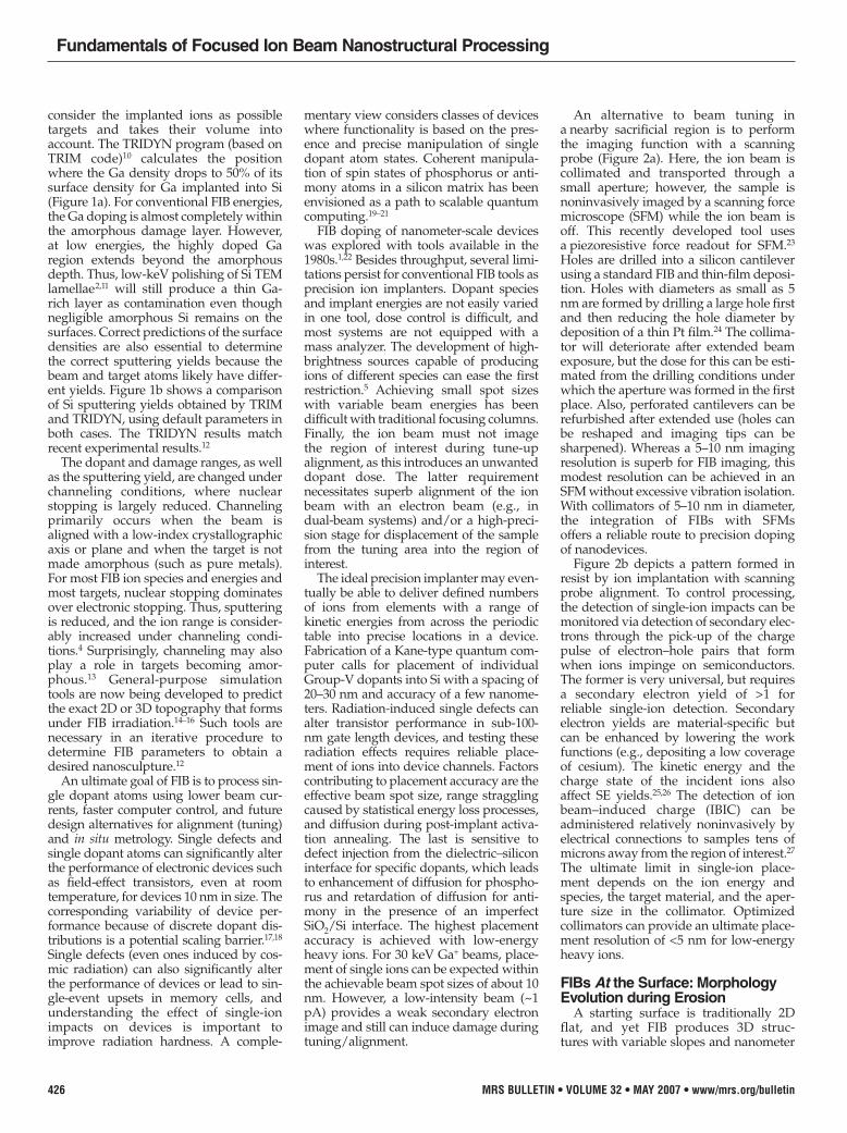
Experimentally, surface topographiesspontaneously develop when targets areeroded by either broad static ion beams ora uniformly rastered FIB.28–40 Althoughroughness is a bane during erosion ofsputter targets used in physical vapordeposition, nanometer-scale structuressuch as ripples (Figure 3a), steps (Figure3b and 3c), and dots (Figure 3d) inspireefforts to understand and manipulate sur-face instabilities. Judicious FIB control has
the potential to fabricate functional arraysof quantum dots.41
Theoretically, if h(x) represents the sur-face topography when the ions approachthe surface in the -z direction, the localheight change at x = (x,y) when an ionstrikes the surface at x¢ is Dh(x;x¢). Duringsputter erosion with an instantaneous ionflux J(x¢), the surface morphology evolu-tion is described by42
. (2)
The complicating aspect of this integralequation is that Dh(x;x¢) depends on thelocal surface slope and curvature, butmay also depend on higher-order deriva-tives. Hence, many theoreticalapproaches start with an approximationfor this “kernel,” Dh(x;x¢). Sigmund firstidentified an instability by assuming thekernel to be proportional to the nuclearenergy deposition density at x in a colli-sion cascade arising from an impact at x¢and approximating the cascade shape
with Gaussian ellipsoids beneath the sur-face.28 Because concave regions of thesurface are nearer their neighboring cas-cades than are convex regions, the pre-dicted sputter yield is higher in theconcave regions, leading to a morpholog-ical instability. By combining the kineticsof surface diffusion with an expansion ofthe Sigmund kernel in Equation 2,Bradley and Harper31 provided a linearstability theory that predicted rippleswith a characteristic spatial scale.Supplements to the theory are higher-order expansions, surface diffusion,31,35,43
viscous flow,32 shadowing,33 crystallo-graphic channeling effects,44,45 redeposi-tion,46 and wave mechanics.47,48
Surface modulations are an intrinsicaspect of the ion erosion process, whethercreated by uniform FIB rastering or by abroad static beam.36,49 Ripple orientation,wavelength, and amplitude depend onenergy, dose, dose rate, inclination angle,temperature, and crystallography, as wellas the ion and surface species. All of theseparameters are similarly controlled forFIB2 or broad-beam processing; however,
J (x′) ∆h (x; x′)d2x′∂h(x, t)
=∂t ∫∫
Fundamentals of Focused Ion Beam Nanostructural Processing
MRS BULLETIN • VOLUME 32 • MAY 2007 • www/mrs.org/bulletin 427
Figure 3. (a) Trenches milled with a Ga-FIB guide self-organized rippling on Si(001) at540ºC under subsequent broad 800 eV Ar+ beam at 45º from normal, projected beamvertical in image as shown (see Reference 52). (b) Scanning electron microscopy (SEM)image of diamond, showing three intersecting surfaces after FIB sputtering. Each surfacewas sputtered in equivalent near-grazing incidence geometry. (c) Cross-sectionaltransmission electron microscopy image of steps formed in diamond after FIB exposure ata high angle of incidence indicated by white arrow (from Reference 53). (d) SEM image ofberyllium surface after Ga-FIB dose of ~8 ¥ 1018 ions/cm2 at ±3º from normal. (Morphologychanges in neighboring grain; see Reference 63.)
MRSBull_May07_Moberly_Final.qxd 5/7/07 6:19 PM Page 427

FIB enables higher current densities and3D forms. FIB dwell time, spot size, over-lap, scan pattern, and orientation providea flexible group of parameters that can becontrolled to produce intrinsic modula-tions; however, stepping outside limits(e.g., large negative overlap) can induceartificial ripples50 that may be more aptlydesignated as patterning. The FIB’s fastcomputer control of precise patterns andparameters can produce nanometer-scale,site-specific modulations and opportuni-ties for rapid prototyping of developingsurface morphologies,39,49,51 especiallywith real-time imaging and in situ (dual-beam) metrology.36,37,39,50
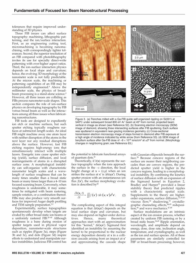
Often a compound process includingFIB will generate geometries that necessi-tate understanding boundary conditions.For example, prepatterned trenches(Figure 3a) influence the subsequent rip-ple development.52 This structure could bemade with photolithography followed bybroad-beam processing, or trenches couldbe direct-written with an FIB to seedspecific instabilities in successive FIBprocesses. Aziz and co-workers haveobserved several effects near boundaries,such as ripple reflection and interfer-ence49 and ripple alignment with thesides of an FIB pit.39 Wavelength canincrease near walls.50 Steeply sloped wallsmay propagate under uniform irradiationas shock fronts (Figure 4).47 A range ofhigh and low slopes all spontaneouslyevolve to the same final value. Whereasnormal processing conditions may “smearout” initial features such as sharp edges,shock mechanics may provide a new levelof nanoscale processing control, in whicha dispersion of initial shapes all convergeto identical final shapes under uniformirradiation.47
FIB ripples have been fashioned oncrystalline36,37,39,45,49,53,54 and amorphous32,36
materials and even on frozen biologicalsamples.55 Ripples can be expected onamorphous surfaces based on theBradley–Harper (B–H) theory,31 and simi-larly the FIB can rapidly make crystallinesurfaces become amorphous and then rip-ple. Even with an amorphous surface,some ripples may exhibit an orientationdependence on subsurface sample crystal-lography.56 Modulations tend to facet oncrystalline surfaces that do not becomeamorphous, but no theory correspondingto B–H covers instabilities on faceting sur-faces. Single-crystal silicon provides anideal surface for the study of variousprocess controls on surface topogra-phies,33,35,49,57 as well as being of practicalimportance to facilitate such topographi-cal control into device applications builton silicon technology.
Diamonds also provide beautiful rip-ples,36,40,50,53,58,59 with the optimization ofFIB processing of micromachining tool-bits53 providing an ideal study of the inter-action of angle, yields, chemistry, andripples. By increasing the angle of ion inci-dence, Adams53 and Datta36 observe threeclassic regimes: smooth, 1D ripples, andsteps (Figure 3b). In fact, the smoothregime can produce surfaces smootherthan the original.50,53 Because a smoothamorphous surface contradicts B–H the-ory, some improvements to the Sigmundkernel are needed.42 A smooth surface fin-ish is typically requested of micromachin-ing, and chemically enhanced FIB iscommonly applied to reduce surfaceroughness.53,60 However, more recentwork uses the same chemistry to enhanceripple growth.50
Since yield depends on local slope,28 theetch rate changes as ripples take shape. Itis not always possible to achieve a steady-state etch rate with constant ripple wave-length and amplitude, and no presenttheory can reliably predict morphologyevolution. Ripple wavelength can increasewith dose57 or be constant,35 and ripplescan be traveling waves,37 with enhancedmobility facilitated by line defects. Mostoften amplitudes saturate at a small frac-
tion of wavelength.33,43,40,57 However,modulations with high aspect ratio39,49,50
offer intriguing possibilities, such as forhigh-surface-area catalysts. Many modelsand experiments indicate the wavelengthsaturates as a function of fluence, which isof practical utility to reliable future FIBprocesses.33,36,43,57 Sigmund’s theory28 hasyield increasing as ripples grow, butCarter61 models a subsequent decrease inyield as wavelength increases. Theyield/ripple dependence is further com-plicated for compound materials thatexhibit a compositional transient periodbefore stabilizing yield.62 Escalating rede-position in a deepening FIB pit can causeripple wavelength to increase with aspectratio while the yield decreases.50 Althoughchemical enhancement of sputter yield istypically designed to provide smoothersurfaces in semiconductor processing, thechemical vapor may also aid ripplegrowth.50 FIB issues that cause ripples togrow too large bode poorly for their use asnanostructures; however, recent FIB pro-cessing of a diamond-like film has alsoproduced subnanometer ripples.63 Even atthe micron scale, understanding the influ-ence of aspect ratio on yield is critical forprecision machining64 and TEM samplepreparation.65 Because ripples change
Fundamentals of Focused Ion Beam Nanostructural Processing
428 MRS BULLETIN • VOLUME 32 • MAY 2007 • www/mrs.org/bulletin
Figure 4. Controlled by shock mechanics, uniform FIB irradiation can cause features tosharpen up rather than to dissipate as expected. Edge of FIB-fabricated pit propagateslaterally under uniformly rastered FIB irradiation (“evolution pit”), while the slope evolvesdownward to a dynamically selected value (“shock front”). A portion of the slope is evolvingupward toward the same dynamically selected value (“unintentional shock front”). (FromReference 47.)
MRSBull_May07_Moberly_Final.qxd 5/7/07 6:19 PM Page 428
Fundamentals of Focused Ion Beam Nanostructural Processing
MRS BULLETIN • VOLUME 32 • MAY 2007 • www/mrs.org/bulletin 429
yield and yield changes ripples, the etchrate may not be treated as constant in FIBprocessing of 3D nanostructures.
Redeposition (or recondensation) isoften hard to avoid during FIB process-ing50,51,66,67 and may play a role in rippleformation.31,68 Special sample geometriesand versatile FIB angles of incidence canlimit redeposition47 and are especially crit-ical for micromachining applications64
and TEM sample preparation.65 Becauseredeposition refers to all cases of atomsreturning to surfaces and may include theinterplay of multiple neighboring sur-faces, ripples at the bottom of an FIB pit39
are modified by redeposition and drop-ping yields.61 Because redeposition can bemeasurable in a micron-size FIB pit evenat low aspect ratios,50 it may similarlyaffect nanometer-scale ripple formationregardless of the beam size46,63 (e.g., usingmodeling parameters in the computerprogram Kalypso69). Modeling of redepo-sition—and its avoidance—is a major con-cern in TEM preparation.66 Trajectorymodels69 show that atoms leaving a sur-face with low kinetic energy may return,depending on surface geometry and therelative charge state between atom andsurface, with the latter being influencedby the incident ions and exiting secondaryelectrons. Erosion ripples can also be aconsequence of laser machining and asso-ciated redeposition;70–73 however, FIBoffers more precise and reliable control ofthese nanometer-scale topographies.
The modern FIB commonly operateswith 30 keV Ga ions, resulting in manysurfaces that are amorphous. The top atomlayers contain more than 10% gallium afterFIB.64,74,75 These artifacts may place practi-cal limits on the use of these modified sur-faces. It may be possible to restorecrystallinity by continued ion bombard-ment,76 as well as by thermal annealing.A chemical etch may remove gallium butmay also disrupt the FIB-processedshapes, especially when gallium composi-tion is also modulated. Residual galliummay limit the utility of self-organizing 2Ddot arrays processed by FIB,49,63 as well asthose integrated with direct-write FIBlithography.41,77,78 However, ripples ofundesirable chemistry and ripples at thebottom of an FIB pit may become usefulafter imprint patterning transfers suchmodulated topographies to the top ofnanometer-scale pedestals. The presentdevelopment of multisource FIBs usinginert ions will facilitate more chemicallycompatible surface structures.
FIBs Above the Surface: FIB–CVDFIB-assisted chemical vapor deposition
(FIB–CVD)79–85 provides an approach to
produce nanostructures above a surface.FIB–CVD is essentially a thin-film growthtechnique that can be used for site-specificdeposition of various materials. ModernFIB systems are capable of depositingmetals, oxides, and carbon with spatialresolution that is often better than electronbeam lithography. Encompassing self-organization processes and predepositedmolecular catalysts, FIB–CVD may alsoproduce yet smaller structures within asingle local pattern.
FIB–CVD involves directing a focusedion beam onto a surface that has adsorbeda precursor gas (e.g., an organometallic)having an element or compound intendedfor deposition as a constituent. The FIBstrikes the surface layer and activates thebreak-up of the molecular species, therebyleading to deposition. Typically, thegaseous precursor species are delivered toa surface by a nearby capillary tube, a noz-zle, or sample box having an opening forbeam entry. This establishes a local pres-sure between 0.1 and 10 mTorr,86,87 yetretains ~10-6 Torr in the remaining vac-uum chamber. The precursor must bevolatile for delivery to the surface, yet itmust adsorb in sufficient quantity88 to cre-ate a deposit upon beam stimulation.
Various processes influence FIB–CVD,including the effects of gas delivery, site-specific adsorption/desorption, surfacemigration, dissociation, incorporation ofimpurities, implantation, sputtering, andthe beam scan parameters (including ioncurrent density).1,89–92 Specialty nozzlesassist growth of and onto complex 3Dgeometries.93 In general, molecular dissoci-ation occurs upon ion bombardment, and adeposit can grow in thickness providedthat sputtering or other competing removalprocesses do not occur at larger rates.Examples of precursor gases include tung-sten hexacarbonyl [W(CO)6], trimethylaluminum [Al(CH3)3], tetraethoxysilane(TEOS), and Cu(I) hexafluoroacetylaceto-nate vinyltrimethylsilane.
Many earlier studies have created sev-eral key applications for FIB and are thefoundations for today’s prototyping6,94,95
and advanced materials analyses.44,96
FIB–CVD is commercially successfulfor semiconductor device restructuringand lithographic mask repair.97,98 Forexample, opaque carbon is producedwhen Ga-FIB energizes adsorbed organicmonomers.82,88,99,100 This provides amethod for correcting clear photomaskdefects in a one-step process.
More recently, FIB–CVD was used forfabricating nanometer-scale sensors101,102
and devices,103 making electrical contactsto nanostructures,104 and joining for lift-out specimens for TEM.2,30 This deposi-
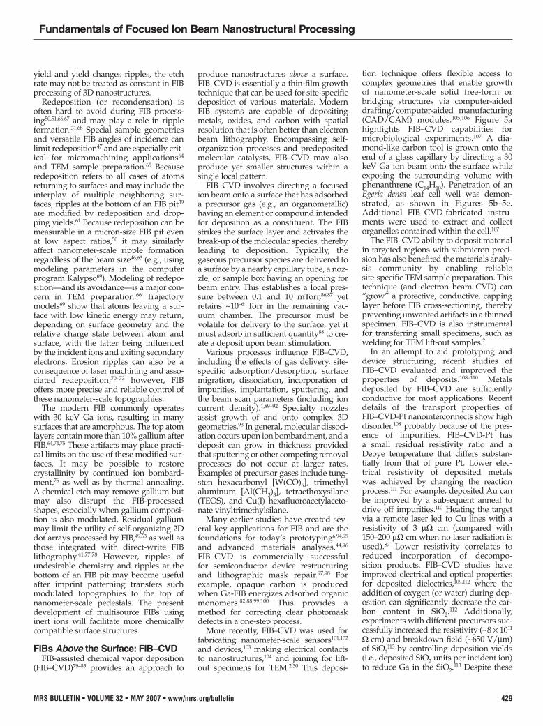
tion technique offers flexible access tocomplex geometries that enable growthof nanometer-scale solid free-form orbridging structures via computer-aideddrafting/computer-aided manufacturing(CAD/CAM) modules.105,106 Figure 5ahighlights FIB–CVD capabilities formicrobiological experiments.107 A dia-mond-like carbon tool is grown onto theend of a glass capillary by directing a 30keV Ga ion beam onto the surface whileexposing the surrounding volume withphenanthrene (C14H10). Penetration of anEgeria densa leaf cell well was demon-strated, as shown in Figures 5b–5e.Additional FIB–CVD-fabricated instru-ments were used to extract and collectorganelles contained within the cell.107
The FIB–CVD ability to deposit materialin targeted regions with submicron preci-sion has also benefited the materials analy-sis community by enabling reliablesite-specific TEM sample preparation. Thistechnique (and electron beam CVD) can“grow” a protective, conductive, cappinglayer before FIB cross-sectioning, therebypreventing unwanted artifacts in a thinnedspecimen. FIB–CVD is also instrumentalfor transferring small specimens, such aswelding for TEM lift-out samples.2
In an attempt to aid prototyping anddevice structuring, recent studies ofFIB–CVD evaluated and improved theproperties of deposits.108–110 Metalsdeposited by FIB–CVD are sufficientlyconductive for most applications. Recentdetails of the transport properties ofFIB–CVD-Pt nanointerconnects show highdisorder,108 probably because of the pres-ence of impurities. FIB–CVD-Pt hasa small residual resistivity ratio and aDebye temperature that differs substan-tially from that of pure Pt. Lower elec-trical resistivity of deposited metalswas achieved by changing the reactionprocess.111 For example, deposited Au canbe improved by a subsequent anneal todrive off impurities.110 Heating the targetvia a remote laser led to Cu lines with aresistivity of 3 mW cm (compared with150–200 mW cm when no laser radiation isused).87 Lower resistivity correlates toreduced incorporation of decompo-sition products. FIB–CVD studies haveimproved electrical and optical propertiesfor deposited dielectrics,109,112 where theaddition of oxygen (or water) during dep-osition can significantly decrease the car-bon content in SiO2.
112 Additionally,experiments with different precursors suc-cessfully increased the resistivity (~8 ¥ 1011
W cm) and breakdown field (~650 V/mm)of SiO2
113 by controlling deposition yields(i.e., deposited SiO2 units per incident ion)to reduce Ga in the SiO2.
113 Despite these
MRSBull_May07_Moberly_Final.qxd 5/7/07 6:19 PM Page 429
improvements, there is little knownregarding conduction and the role ofdefects in insulators made by FIB–CVD.Finally, the mechanical properties ofmaterials made by FIB–CVD were evalu-ated114–116 for potential structural applica-tions such as those involving cell cuttingand nanomanipulation. Recent studieshave quantified the Young’s modulus(~100 GPa), shear modulus (~70 GPa), andspring constants (0.47–0.07 N/m) of dia-mond-like carbon grown by FIB–CVD.116
Ga is incorporated into deposits madeby FIB–CVD with estimates of Ga concen-tration as high as 28 mol%117 that maylimit the usefulness of some structures.Future FIB development will offer lessinvasive ion species.118 Nevertheless, thesite-specificity of Ga-FIB–CVD outweighsthe contamination effects for many appli-cations.1,2,92,97,98,119
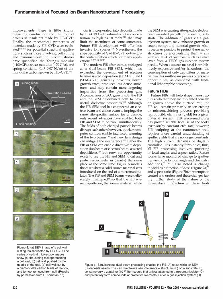
The modern FIB often comes packagedas a dual-beam FIB–SEM, which hasexpanded the development of electronbeam–assisted deposition (EBAD). EBAD(SEM–CVD) generally provides slowergrowth rates, produces less dense struc-tures, and may contain more lingeringimpurities from the processing gas.A comparison of SiO2 grown with the FIBand the SEM determined both to haveuseful dielectric properties.109 Althoughthe FIB–SEM tool has engineered an elec-tron beam and an ion beam to impinge thesame site-specific surface for a decade,only recent advances have enabled bothFIB and SEM to be “on” simultaneously.The fields of both charged particle beamsdisrupt each other; however, quicker com-puter controls enable interlaced scanningof the two beams120 and new lens designcan mitigate the interference.121 Either theFIB or SEM can enable direct-write depo-sition (ion beam or electron beam–assisteddeposition),109 but now the opportunityexists to use the FIB and SEM to cut andpaste, respectively, in (nearly) the sameplace at the same time. Figure 6 modelsthe case where a solid source material wasintroduced on the end of a micromanipu-lator. The FIB and SEM beams were delib-erately misaligned63 so that the FIB wasnanosputtering the source material while
the SEM was causing site-specific electronbeam–assisted growth on a nearby sub-strate. The addition of gases via a gas-injection system may enhance growth orenable compound material growth. Also,it becomes possible to protect these nano-structures by encapsulating them in situwith an FIB–CVD overcoat, such as a silicalayer from a TEOS gas-injection systemneedle. When a source material is prohib-itively expensive and/or hazardous, theconsumption of only zeptoliters of mate-rial via this multibeam process offers newopportunities, as compared with tradi-tional lithographic processing.
Future FIBsFuture FIBs will help shape nanostruc-
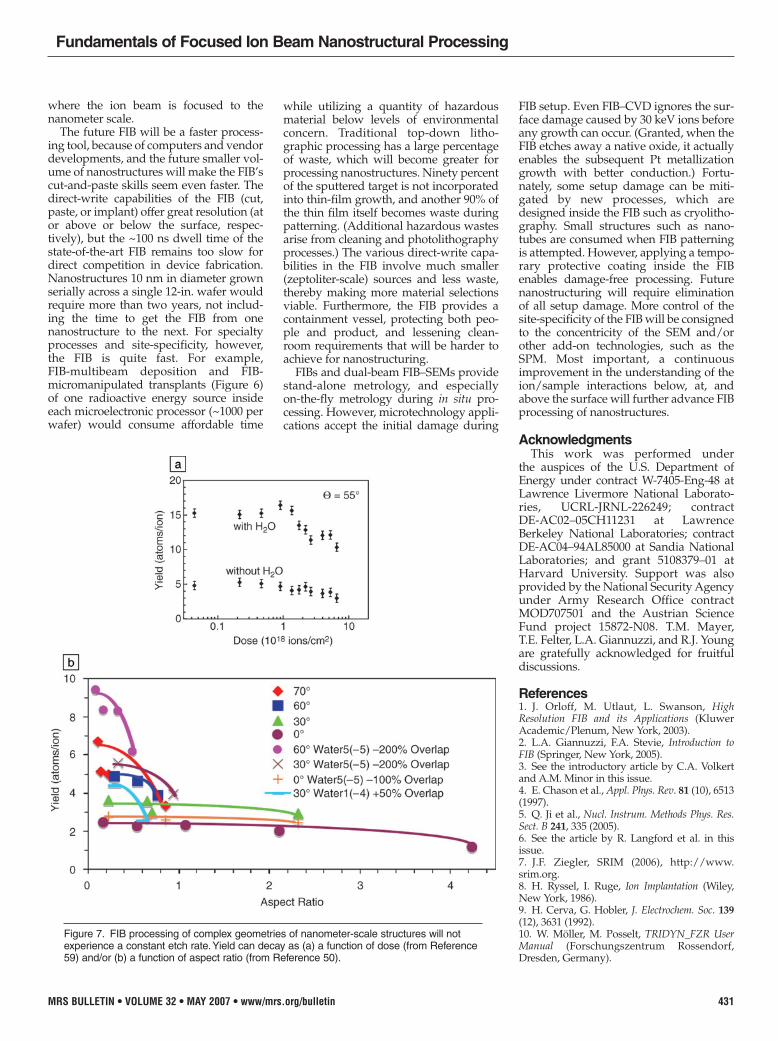
tures, whether they are implanted beneathor grown above the surface. Yet, theFIB will remain primarily an ion etchingor micromachining process providingreproducible etch rates (yield) for a givenmaterial system. FIB micromachininghas proven reliable because of the tool’strustworthy constant etch rate; however,FIB sculpting at the nanometer scalerequires more careful understanding ofsputter yields that are no longer constants.The high current densities of digitallycontrolled FIBs instantly form holes; thus,all FIB processing involves sputteringof local angles and aspect ratios. Recentworks have monitored change to sputter-ing yield due to local angle and chemistryadditions,53 but also noted a changein yield as a function of dose (Figure 7a)59
and aspect ratio (Figure 7b).50 Attempts tocontrol and understand these changes jus-tify further study of the nature of theion–surface interaction in these tools
Fundamentals of Focused Ion Beam Nanostructural Processing
430 MRS BULLETIN • VOLUME 32 • MAY 2007 • www/mrs.org/bulletin
Figure 5. (a) SEM image of a cell wallcutting tool fabricated by FIB–CVD. Theseries of optical microscope imagesshow (b) the cutting tool approachinga cell wall, (c) cell wall pushed by theneedle of the tool, (d) cell wall cut bya diamond-like carbon blade of the tool,and (e) tool removed from cell. (Resultsby permission from R. Kometani.107)
Figure 6. Simultaneous dual-beam processing enables the FIB (A) to cut while an SEM(B) deposits nearby. This can direct-write nanometer-scale structures (F) on a substrate (E),consume only a zeptoliter (10-21 liter) source that arrives attached to a micromanipulator (C)and potentially form compounds or protective overcoats (G) via a gas-injection system (D).
MRSBull_May07_Moberly_Final.qxd 5/7/07 6:19 PM Page 430
Fundamentals of Focused Ion Beam Nanostructural Processing
MRS BULLETIN • VOLUME 32 • MAY 2007 • www/mrs.org/bulletin 431
where the ion beam is focused to thenanometer scale.
The future FIB will be a faster process-ing tool, because of computers and vendordevelopments, and the future smaller vol-ume of nanostructures will make the FIB’scut-and-paste skills seem even faster. Thedirect-write capabilities of the FIB (cut,paste, or implant) offer great resolution (ator above or below the surface, respec-tively), but the ~100 ns dwell time of thestate-of-the-art FIB remains too slow fordirect competition in device fabrication.Nanostructures 10 nm in diameter grownserially across a single 12-in. wafer wouldrequire more than two years, not includ-ing the time to get the FIB from onenanostructure to the next. For specialtyprocesses and site-specificity, however,the FIB is quite fast. For example,FIB-multibeam deposition and FIB-micromanipulated transplants (Figure 6)of one radioactive energy source insideeach microelectronic processor (~1000 perwafer) would consume affordable time
while utilizing a quantity of hazardousmaterial below levels of environmentalconcern. Traditional top-down litho-graphic processing has a large percentageof waste, which will become greater forprocessing nanostructures. Ninety percentof the sputtered target is not incorporatedinto thin-film growth, and another 90% ofthe thin film itself becomes waste duringpatterning. (Additional hazardous wastesarise from cleaning and photolithographyprocesses.) The various direct-write capa-bilities in the FIB involve much smaller(zeptoliter-scale) sources and less waste,thereby making more material selectionsviable. Furthermore, the FIB provides acontainment vessel, protecting both peo-ple and product, and lessening clean-room requirements that will be harder toachieve for nanostructuring.
FIBs and dual-beam FIB–SEMs providestand-alone metrology, and especiallyon-the-fly metrology during in situ pro-cessing. However, microtechnology appli-cations accept the initial damage during
FIB setup. Even FIB–CVD ignores the sur-face damage caused by 30 keV ions beforeany growth can occur. (Granted, when theFIB etches away a native oxide, it actuallyenables the subsequent Pt metallizationgrowth with better conduction.) Fortu-nately, some setup damage can be miti-gated by new processes, which aredesigned inside the FIB such as cryolitho-graphy. Small structures such as nano-tubes are consumed when FIB patterningis attempted. However, applying a tempo-rary protective coating inside the FIBenables damage-free processing. Futurenanostructuring will require eliminationof all setup damage. More control of thesite-specificity of the FIB will be consignedto the concentricity of the SEM and/orother add-on technologies, such as theSPM. Most important, a continuousimprovement in the understanding of theion/sample interactions below, at, andabove the surface will further advance FIBprocessing of nanostructures.
AcknowledgmentsThis work was performed under
the auspices of the U.S. Department ofEnergy under contract W-7405-Eng-48 atLawrence Livermore National Laborato-ries, UCRL-JRNL-226249; contractDE-AC02–05CH11231 at LawrenceBerkeley National Laboratories; contractDE-AC04–94AL85000 at Sandia NationalLaboratories; and grant 5108379–01 atHarvard University. Support was alsoprovided by the National Security Agencyunder Army Research Office contractMOD707501 and the Austrian ScienceFund project 15872-N08. T.M. Mayer,T.E. Felter, L.A. Giannuzzi, and R.J. Youngare gratefully acknowledged for fruitfuldiscussions.
References1. J. Orloff, M. Utlaut, L. Swanson, HighResolution FIB and its Applications (KluwerAcademic/Plenum, New York, 2003).2. L.A. Giannuzzi, F.A. Stevie, Introduction toFIB (Springer, New York, 2005).3. See the introductory article by C.A. Volkertand A.M. Minor in this issue.4. E. Chason et al., Appl. Phys. Rev. 81 (10), 6513(1997).5. Q. Ji et al., Nucl. Instrum. Methods Phys. Res.Sect. B 241, 335 (2005).6. See the article by R. Langford et al. in thisissue.7. J.F. Ziegler, SRIM (2006), http://www.srim.org.8. H. Ryssel, I. Ruge, Ion Implantation (Wiley,New York, 1986).9. H. Cerva, G. Hobler, J. Electrochem. Soc. 139(12), 3631 (1992).10. W. Möller, M. Posselt, TRIDYN_FZR UserManual (Forschungszentrum Rossendorf,Dresden, Germany).
Figure 7. FIB processing of complex geometries of nanometer-scale structures will notexperience a constant etch rate.Yield can decay as (a) a function of dose (from Reference59) and/or (b) a function of aspect ratio (from Reference 50).
MRSBull_May07_Moberly_Final.qxd 5/7/07 6:20 PM Page 431

11. L.A. Giannuzzi, Microsc. Microanal. 12 (2),1260 (2006).12. D.P. Adams, M.J. Vasile, J. Vac. Sci. Technol.,B 24 (2), 836 (2006).13. A. Lugstein, W. Brezna, G. Hobler, E.Bertagnolli, J. Vac. Sci. Technol., A 21, 1644 (2003).14. G. Hobler, A. Lugstein, W. Brezna, E.Bertagnolli, in Mater. Res. Soc. Symp. Proc. 792,L.-M. Wang et al., Eds. (Warrendale, PA, 2003)pp. 635–640.15. H.B. Kim, G. Hobler, A. Lugstein, E.Bertagnolli, J. Micromech. Microeng. (2007) inpress.16. W. Boxleitner, G. Hobler, Nucl. Instrum.Methods Phys. Res., Sect. B 180, 125 (2001).17. T. Shinada, S. Okamoto, T. Kobayashi, I.Ohdomari, Nature 437, 1128 (2005).18. T. Schenkel, Nature Mater. 4, 799 (2005).19. B.E. Kane, Nature 393, 133 (1998).20. T. Schenkel et al., Appl. Phys. Lett. 88, 112101(2006).21. R.G. Clark et al., Philos. Trans. R. Soc.London, Ser. A, 361, 1451 (2003).22. R.H. Reuss et al., J. Vac. Sci. Technol., B 4, 290(1986).23. A. Persaud et al., Nano Lett. 5, 1087 (2005).24. T. Schenkel et al., J. Vac. Sci. Technol., B 21,2720 (2003).25. R.A. Baragiola, Nucl. Instrum. Methods Phys.Res. B 78, 223 (1993).26. T. Schenkel et al., Microelectron. Eng. 8, 1814(2006).27. D.N. Jamieson et al., Appl. Phys. Lett. 86,202101 (2005).28. P. Sigmund, J. Mater. Sci. 8, 1545 (1973).29. B.R. Appleton et al., Appl. Phys. Lett. 41 (8),711 (1982).30. F.A. Stevie, P.M. Kahora, D.S. Simons, P.Chi, J. Vac. Sci. Technol., A 6, 76 (1988).31. R.M. Bradley, J.M.E. Harper, J. Vac. Sci.Technol., A 6, 2390 (1988).32. T.M. Mayer, E. Chason, A.J. Howard,J. Appl. Phys. 76 (3), 1634 (1994).33. G. Carter, V. Vishnyakov, Phys. Rev. B 54,17647 (1996).34. S. Facsko et al., Science 285, 1551 (1999).35. J. Erlebacher et al., Phys. Rev. Lett. 82 (11),2330 (1999).36. A. Datta, Y.R. Wu, Y.L. Wang, Phys. Rev. B63, 125407 (2001).37. S. Habenicht, K.P. Lieb, J. Koch, A.D. Wieck,Phys. Rev. B 65, 115327 (2002).38. W.L Chan, N. Pavenayotin, E. Chason,Phys. Rev. B 69, 245413 (2004).39. S. Ichim, M.J. Aziz, J. Vac. Sci. Technol., B 23,1068 (2005).40. T.M. Mayer, D.P. Adams, M.J. Vasile, K.M.Archuleta, J. Vac. Sci. Technol., A 23, 1579 (2005).41. J.L. Gray, S. Atha, R. Hull, J.A. Floro, NanoLett. 4 (12), 2447 (2004).42. M.J. Aziz, Mat. Fys. Medd. Dan Vid Selsk(2006) in press.43. M.A. Makeev, R. Cuerno, A.L. Barabasi,Nucl. Instrum. Methods Phys. Res., Sect. B 197,185 (2002).44. R. Levi-Setti, T.R. Fox, K. Lam, Nucl. Instr.Meth. 205, 299 (1983).45. B.W. Kempshall et al., J. Vac. Sci. Technol., B19, 729 (2001).46. M. Castro, R. Cuerno, L. Vazquez, R. Gago,Phys. Rev. Lett. 94, 016102 (2005).47. H.H. Chen et al., Science 310, 294 (2005).
48. J. Teichert, L. Bischoff, B. Kohler, Appl. Phys.Lett. 69 (11), 1544 (1996).49. A. Cuenat, M.J. Aziz, in Mater. Res. Soc.Symp. Proc. 696, E.A. Stach, E.H. Chason, R. Hull,S.D. Bader, Eds. (2002) pp. 31–36.50. W.J. MoberlyChan, T.E. Felter, M.A. Wall,Microsc. Today, 28 (November 2006).51. D. Santamore, K. Edinger, J. Orloff,J. Melngailis, J. Vac. Sci. Technol., B 15, 2346 (1997).52. A. Cuenat, Adv. Mater. 17, 2845 (2005).53. D.P. Adams, M.J. Vasile, T.M. Mayer, V.C.Hodges, J. Vac. Sci. Technol., B 21, 2334 (2003).54. U. Wendt, G. Nolze, H. Heyse, Microsc.Microanal. 12 (suppl. 2), 1302 (2006).55. W.J. MoberlyChan, S. Reyntjens, A.M.Minor, Microsc. Microanal. 12 (suppl. 2), 1268(2006).56. U. Valbusa, C. Boragno, F. Buatier deMongeot, J. Phys.: Condens. Matter 14, 8153 (2002).57. A.D. Brown, J. Erlebacher, W.L. Chan, E.Chason, Phys. Rev. Lett. 95, 056101 (2005).58. A. Stanishevsky, Thin Solid Films 398–399,560 (2001).59. D.P. Adams, T.M. Mayer, M.J. Vasile, K.Archuleta, Appl. Surf. Sci. 252, 2432 (2006).60. P.E. Russell et al., J. Vac. Sci. Technol., B 16(4), 2494 (1998).61. G. Carter, J. Appl. Phys. 85 (1), 455 (1999).62. A. Lugstein, B. Basnor, E. Bertagnolli, J. Vac.Sci. Technol., B 20, 2238 (2002).63. W.J. MoberlyChan, Mater. Res. Soc. Symp.Proc. 960, N10-02 (2006).64. D.P. Adams, M.J. Vasile, T.M. Mayer, J. Vac.Sci. Technol., B 24 (4), 1766 (2006).65. T. Ishitani, T. Yaguchi, Microsc. Res. Technol.35, 320 (1996).66. T. Ihsitani, T. Ohnishi, J. Vac. Sci. Technol., A9, 3084 (1991).67. M.J. Vasile, J. Xie, R. Nassar, J. Vac. Sci.Technol., B 17 (6), 3085 (1999).68. S. Facsko et al., Phys. Rev. B 69, 153412 (2004).69. M.A. Karolewski, Nucl. Instrum. MethodsPhys. Res., Sect. B 230, 402 (2005); Kalypsosoftware, www.geocities.com/karolewski/Kalypso.70. P. Tosin, A. Blatter, W. Luthy, J. Appl. Phys.76 (6), 3797 (1995).71. A.M. Ozhan et al., Appl. Phys. Lett. 75 (23),3716 (1999).72. E. Coyne, J. Magee, P. Mannion, G.O’Connor, Proc. SPIE 4876, 487 (2003).73. J.N. Brooks, Fusion Eng. Des. 60, 515 (2002).74. T. Ishitani, H. Koike, T. Yaguchi, T. Kamino,J. Vac. Sci. Technol., B 16 (4), 1907 (1998).75. J.R. Michael, Microsc. Microanal. 12 (2), 1248(2005).76. G. Carter, Vacuum 80, 475 (2006).77. M. Kammler, R. Hull, M.C. Reuter, F.M.Ross, Appl. Phys. Lett. 82, 1903 (2003).78. A.A. Bergman et al., Langmuir 14, 6785 (1998).79. K. Gamo et al., Jpn. J. Appl. Phys. 23, L293(1984).80. G.M. Shedd, H. Lezec, A.D. Dubner,J. Melngailis, Appl. Phys. Lett. 49, 1584 (1986).81. H.C. Kaufmann, W.B. Thompson, G.J.Dunn, Proc. SPIE 632, 60 (1986).82. L.R. Harriott, M.J. Vasile, J. Vac. Sci. Technol.,B 6, 1035 (1988).83. R.L. Kubena, F.P. Stratton, T.M. Mayer,J. Vac. Sci. Technol., B 6, 1865 (1988).84. M.E. Gross, L.R. Harriott, R.L. Opila Jr.,J. Appl. Phys. 68, 4820 (1990).
85. P.G. Blauner, J.S. Ro, Y. Butt, J. Melngailis,J. Vac. Sci. Technol., B 7, 609 (1989).86. R.J. Young, J.R.A. Cleaver, H. Ahmed, J. Vac.Sci. Technol., B 11 (2), 234 (1993).87. J. Funatsu, C.V. Thompson, J. Melngailis,J.N. Walpole, J. Vac. Sci. Technol., B 14, 179(1996).88. M.J. Vasile, L.R. Harriott, J. Vac. Sci. Technol.,B 7, 1954 (1989).89. J.S. Ro, C.V. Thompson, J. Melngailis, ThinSolid Films 258, 333 (1995).90. T.P. Chiang, H.H. Sawin, C.V. Thompson,J. Vac. Sci. Technol., A 15, 3104 (1997).91. A.D. Dubner, A. Wagner, J. Melngailis, C.V.Thompson, J. Appl. Phys. 70, 665 (1991).92. J. Melngailis, Proc. SPIE 1465, 36 (1991).93. V. Ray, J. Vac. Sci. Technol., B 22 (6), 3008(2004).94. T. Ishitani, T. Ohnishi, Y. Kawanami, Jpn.J. Appl. Phys. 29, 2283 (1990).95. M.J. Vasile et al., Rev. Sci. Instrum. 62, 2167(1991).96. See the article by M. Uchic et al. in thisissue.97. J. Melngailis, J. Vac. Sci. Technol., B 5, 469(1987).98. L.R. Harriott, Appl. Surf. Sci. 36, 432 (1989).99. W.P. Economou, D.C. Shaver, B. Ward, Proc.SPIE 773, 201 (1987).100. M. Yamamoto et al., Proc. SPIE 632, 97(1986).101. R. Puers, S. Reyntjens, D. De Bruyker, Sens.Actuators, A 97–98, 208 (2002).102. S. Khizroev, J.A. Bain, D. Litvinov,Nanotechnology 13, 619 (2002).103. E.M. Ford, H. Ahmed, Appl. Phys. Lett. 75,421 (1999).104. T.W. Ebbesen et al., Nature 382, 54 (1996).105. A.J. Demarco, J. Melngailis, J. Vac. Sci.Technol., B 17, 3154 (1999).106. T. Morita et al., J. Vac. Sci. Technol., B 21,2737 (2003).107. R. Kometani et al., Microelectron. Eng. 83,1642 (2006).108. J.-F. Lin, J.P. Bird, L. Rotkina, P.A. Bennett,Appl. Phys. Lett. 82, 802 (2003).109. E.J. Sanchez, J.T. Krug, X.S. Xie, Rev. Sci.Instrum. 73 (11), 3901 (2002).110. A. Botman, J.J.L. Mulders, R. Weemaes, S.Mentink, Nanotechnology 17, 3779 (2006).111. P.G. Blauner et al., J. Vac. Sci. Technol., B 7,1816 (1989).112. A.N. Campbell et al., Proc. 23rd Int. Symp.Testing Failure Analysis (1997) p. 223.113. K. Edinger, J. Melngailis, J. Orloff, J. Vac.Sci. Technol., B 16, 3311 (1998).114. S. Reyntjens, R. Puers, J. Micromech.Microeng. 10, 181 (2000).115. M. Ishida et al., J. Vac. Sci. Technol., B 21,2728 (2003).116. K.-I. Nakamatsu et al., J. Vac. Sci. Technol.,B 23, 2801 (2005).117. T. Tao, J. Ro, J. Melngailis, J. Vac. Sci.Technol., B 8, 1826 (1990).118. N. Smith et al., J. Vac. Sci. Technol., B 24 (6),2902 (2006).119. T.M. Mayer, S.D. Allen, Thin Film ProcessesII, J.L. Vossen, W. Kern, Eds. (Academic Press,New York, 1991) pp. 621–670.120. FEI Co. SPI-mode technology, www.feico.com.121. Zeiss technology, www.smt.zeiss.com/nts. ■■
Fundamentals of Focused Ion Beam Nanostructural Processing
432 MRS BULLETIN • VOLUME 32 • MAY 2007 • www/mrs.org/bulletin
MRSBull_May07_Moberly_Final.qxd 5/7/07 6:20 PM Page 432

MRSBull_May07_Moberly_Final.qxd 5/7/07 6:20 PM Page 433