serial video links in automotive applications
TRANSCRIPT
Department of Science and Technology Institutionen för teknik och naturvetenskap Linköping University Linköpings universitet
gnipökrroN 47 106 nedewS ,gnipökrroN 47 106-ES
LiU-ITN-TEK-A--17/015--SE
Serial Video Links inAutomotive Applications
Oskar von Heideken
Max Wennerfeldt
2017-06-01
LiU-ITN-TEK-A--17/015--SE
Serial Video Links inAutomotive Applications
Examensarbete utfört i Elektroteknikvid Tekniska högskolan vid
Linköpings universitet
Oskar von HeidekenMax Wennerfeldt
Handledare Magnus KarlssonExaminator Qin-Zhong Ye
Norrköping 2017-06-01
Upphovsrätt
Detta dokument hålls tillgängligt på Internet – eller dess framtida ersättare –under en längre tid från publiceringsdatum under förutsättning att inga extra-ordinära omständigheter uppstår.
Tillgång till dokumentet innebär tillstånd för var och en att läsa, ladda ner,skriva ut enstaka kopior för enskilt bruk och att använda det oförändrat förickekommersiell forskning och för undervisning. Överföring av upphovsrättenvid en senare tidpunkt kan inte upphäva detta tillstånd. All annan användning avdokumentet kräver upphovsmannens medgivande. För att garantera äktheten,säkerheten och tillgängligheten finns det lösningar av teknisk och administrativart.
Upphovsmannens ideella rätt innefattar rätt att bli nämnd som upphovsman iden omfattning som god sed kräver vid användning av dokumentet på ovanbeskrivna sätt samt skydd mot att dokumentet ändras eller presenteras i sådanform eller i sådant sammanhang som är kränkande för upphovsmannens litteräraeller konstnärliga anseende eller egenart.
För ytterligare information om Linköping University Electronic Press seförlagets hemsida http://www.ep.liu.se/
Copyright
The publishers will keep this document online on the Internet - or its possiblereplacement - for a considerable time from the date of publication barringexceptional circumstances.
The online availability of the document implies a permanent permission foranyone to read, to download, to print out single copies for your own use and touse it unchanged for any non-commercial research and educational purpose.Subsequent transfers of copyright cannot revoke this permission. All other usesof the document are conditional on the consent of the copyright owner. Thepublisher has taken technical and administrative measures to assure authenticity,security and accessibility.
According to intellectual property law the author has the right to bementioned when his/her work is accessed as described above and to be protectedagainst infringement.
For additional information about the Linköping University Electronic Pressand its procedures for publication and for assurance of document integrity,please refer to its WWW home page: http://www.ep.liu.se/
© Oskar von Heideken, Max Wennerfeldt
Abstract
This thesis investigates the available and upcoming serializer and deseri-alizer solutions for MIPI-CSI 2 camera interface, in order to reduce cablecost and lower installation complexity for mounting satellite cameras inautomotive applications. A market survey was conducted resulting inseveral available and coming solutions. One solution found in the surveywas selected together with Autoliv Sverige AB for further investigationand implementation in the form of a demonstration platform. Due to anon-disclosure agreement between Autoliv Sverige AB and the integratedcircuit manufacturer, part number and name of the manufacturer of theserializer and deserializer circuits will not be disclosed in this report. Theschematic, printed circuit board design and manufacturing of the demon-stration platform were done within the scope of this thesis. Simulations ofcritical sections in the schematic and layout were made in order to ensurestable functionality. The assembled serializer and deserializer units weretested together with a selection of automotive graded cables in order totest the system and establish the best suited cable with regards to cost,weight and performance. The results show that five serializer and deseri-alizer solutions were found and the choice of cables is a trade-off betweenperformance and external factors such as noise and required cable length.

Preface
Gratitude towards Autoliv Sverige AB is extended for providing the task, helpand support that made this thesis possible. Special thanks to Peter Karlen andJohan Moleklint at Autoliv Sverige AB in Linkoping for all the guidance andhelp.
Thanks to Qin-Zhong Ye, Magnus Karlsson and Gustav Knutsson at the depart-ment of science and technology at Linkoping University for guidance, equipmentand help.
Thanks to all afflicted subcontractors to Autoliv Sverige AB providing supportand material.
i

Acronyms
ADAS Advanced Driver Assistance Systems. 1, 91, 99
ADS Advanced Design System 2016 from Keysight Inc. vi, vii, viii, ix, 4, 33,43, 45, 47, 50, 93, A1
BER Bit Error Rate. 14
BGA Ball Grid Array. 66
CDR Clock and Data recovery. 9
CRC Cyclic Redundancy Check. 6
DC Direct Current. 2, 15, 17, 19, 79, 92
DDR Double Data Rate. 8
ECC Error Correcting Code. 6
EM Electromagnetic Model. viii, 50, 52, 93
EMC ElectroMagnetic Compatibility. v, vi, 2, 10, 16, 19, 21, 22, 39, 44, 60,66, 81, 91, 95, 99
EMI ElectroMagnetic Interference. 2, 10, 15, 16, 17, 18, 19, 20, 21, 32, 99
ESR Equivalent Series Resistance. 45
EuroNCAP European New Car Assessment Programme. 1
EVM EValuation Modules. 4
FAKRA Fachkreis Automobil (Automobile Expert Group). 29, 30, 82, 97
Gbps Gigabit per second. 2, 3, 8, 15, 66, 91
GPIO General Purpose Input/Output. 28, 57, 91
HSD High Speed Data (cable). 29, 30, 95, 97
I2C Inter-Integrated Circuit. vii, 6, 8, 34, 35, 38, 39, 44, 56, 57, 62, 66
IC Integrated Circuit. iv, 3, 10, 11, 15, 25, 26, 28, 34, 35, 38, 40, 41, 42, 44,52, 56, 57, 58, 59, 60, 65, 66, 82, 84, 91, 95, 97, 99
IRR Insertion loss to Return loss Ratio. ix, 42, 43, 79, B1
ISI InterSymbol Interference. 13, 14
LVDS Low Voltage Differential Signal. iv, vi, vii, 5, 8, 10, 11, 14, 15, 86, 91
ii

MCU MicroController Unit. viii, x, 28, 34, 35, 38, 39, 56, 57
MIPI Mobile Industry Processor Interface. 5, 6, 8, 34
MIPI DSI Mobile Industry Processor Interface Display Serial Interface. 8
MIPI CSI-2 Mobile Industry Processor Interface Camera Serial Interface 2.iv, vii, 3, 5, 6, 8, 25, 26, 28, 41, 42, 57, 66, 91
MIPI CSI Mobile Industry Processor Interface Camera Serial Interface. iv, x,5, 6, 8, 9
NDA Non-Disclosure Agreement. 2, 3, 4, 8, 25, 26, 35, 45, 57, 62, 65, 79, 91,93
NRZ Non-Return to Zero. 14
PCB Printed Circuit Board. viii, 4, 8, 11, 12, 35, 39, 42, 44, 45, 50, 52, 58, 59,60, 69, 79, 81, 92, 93, 97
PoC Power-over-Coaxial. v, vi, vii, viii, ix, x, 15, 28, 33, 35, 37, 42, 45, 47, 52,59, 62, 66, 69, 73, 76, 79, 82, 84, 85, 86, 89, 92, 93, 95, 99, A1
PoE Power-over-Ethernet. 15
QFN Quad Flat pack No lead. 66
RF Radio Frequency. 29, 30
SATA Serial Advanced Technology Attachment. 8
SerDes Serializer/Deserializer. iv, vii, viii, ix, x, 5, 6, 8, 9, 10, 11, 15, 25, 26,28, 34, 35, 38, 42, 52, 55, 56, 57, 58, 60, 62, 63, 65, 66, 79, 91, 95, 97, 99,B1
SMB SubMiniature version B. 30
SMD Surface Mount Device. 50
SRF Self Resonant Frequency. 12, 15, 20, 45
STP Shielded Twisted Pair. 1, 20, 21, 28, 66, 91
STQ Shielded Twisted Quad. vii, viii, ix, x, 1, 20, 21, 28, 30, 31, 32, 35, 43,50, 52, 55, 73, 76, 86, 93, 95, 99, B1
UART Universal Asynchronous Receiver/Transmitter. 34, 35, 38, 39, 44, 57,60
VP Video Processor. 1, 2, 3, 6, 8, 28, 34, 63, 91
iii

Contents
Preface i
1 Introduction 1
1.1 Purpose . . . . . . . . . . . . . . . . . . . . . . . . . . . . . . . . 11.2 Problem Formulations . . . . . . . . . . . . . . . . . . . . . . . . 21.3 Specification of Requirements . . . . . . . . . . . . . . . . . . . . 21.4 Limitations . . . . . . . . . . . . . . . . . . . . . . . . . . . . . . 31.5 Outline . . . . . . . . . . . . . . . . . . . . . . . . . . . . . . . . 31.6 Method and Materials . . . . . . . . . . . . . . . . . . . . . . . . 4
1.6.1 Material and Sources . . . . . . . . . . . . . . . . . . . . . 41.6.2 Software . . . . . . . . . . . . . . . . . . . . . . . . . . . . 4
2 Background 5
2.1 Proposed System . . . . . . . . . . . . . . . . . . . . . . . . . . . 52.2 Mobile Industry Processor Interface Camera Serial Interface . . . 5
2.2.1 MIPI CSI-2 . . . . . . . . . . . . . . . . . . . . . . . . . . 62.2.2 MIPI D-PHY . . . . . . . . . . . . . . . . . . . . . . . . . 8
2.3 Camera Control Signals . . . . . . . . . . . . . . . . . . . . . . . 82.4 Serializer/Deserializer . . . . . . . . . . . . . . . . . . . . . . . . 8
2.4.1 Serializer . . . . . . . . . . . . . . . . . . . . . . . . . . . 92.4.2 Deserializer . . . . . . . . . . . . . . . . . . . . . . . . . . 10
2.5 Low Voltage Differential Signal . . . . . . . . . . . . . . . . . . . 102.5.1 Design Guidelines for High Speed LVDS . . . . . . . . . . 11
2.5.1.1 Transmission Line Impedance . . . . . . . . . . . 112.5.1.2 Components . . . . . . . . . . . . . . . . . . . . 12
2.5.2 Jitter . . . . . . . . . . . . . . . . . . . . . . . . . . . . . 132.5.3 Low Voltage Differential Signal Integrity Testing . . . . . 14
2.6 Power-over-Ethernet and Power-over-Coaxial . . . . . . . . . . . 152.7 Cables and Electromagnetic Aspects . . . . . . . . . . . . . . . . 16
2.7.1 Cable Shielding . . . . . . . . . . . . . . . . . . . . . . . . 162.7.1.1 Braided Shield . . . . . . . . . . . . . . . . . . . 172.7.1.2 Foiled Shield . . . . . . . . . . . . . . . . . . . . 182.7.1.3 Shielding Effectiveness and Signal Attenuation . 19
2.7.2 Cables . . . . . . . . . . . . . . . . . . . . . . . . . . . . . 202.7.2.1 Twisted Pair . . . . . . . . . . . . . . . . . . . . 202.7.2.2 Shielded Twisted Quad . . . . . . . . . . . . . . 222.7.2.3 Coaxial cables . . . . . . . . . . . . . . . . . . . 22
3 Implementation 25
3.1 SerDes Market Survey . . . . . . . . . . . . . . . . . . . . . . . . 253.2 Choice of SerDes Integrated Circuits . . . . . . . . . . . . . . . . 263.3 System Design . . . . . . . . . . . . . . . . . . . . . . . . . . . . 28
3.3.1 Serializer and Deserializer Integrated Circuits . . . . . . . 283.3.2 High Speed Connector . . . . . . . . . . . . . . . . . . . . 293.3.3 High Speed Data and Power Cable . . . . . . . . . . . . . 303.3.4 Power over Coaxial Filter . . . . . . . . . . . . . . . . . . 333.3.5 Power Management . . . . . . . . . . . . . . . . . . . . . 34
iv

3.3.6 Microcontroller . . . . . . . . . . . . . . . . . . . . . . . . 343.4 Schematics Design . . . . . . . . . . . . . . . . . . . . . . . . . . 35
3.4.1 High Speed Connector Schematics . . . . . . . . . . . . . 353.4.2 Power-Over-Coaxial Filter Schematics . . . . . . . . . . . 373.4.3 Microcontroller Unit and Level Converter Schematic . . . 38
3.5 Printed Circuit Board Layout . . . . . . . . . . . . . . . . . . . . 393.5.1 High Speed Layout Guidelines . . . . . . . . . . . . . . . 403.5.2 MIPI CSI-2 Signal Layout . . . . . . . . . . . . . . . . . . 413.5.3 High Speed Front-End . . . . . . . . . . . . . . . . . . . . 423.5.4 Power Routing . . . . . . . . . . . . . . . . . . . . . . . . 44
3.5.4.1 Low Speed Signal Routing and Passive Compo-nents . . . . . . . . . . . . . . . . . . . . . . . . 45
3.6 Simulation . . . . . . . . . . . . . . . . . . . . . . . . . . . . . . . 453.6.1 Schematics Simulation . . . . . . . . . . . . . . . . . . . . 45
3.6.1.1 PoC Component Equivalent Circuit . . . . . . . 453.6.1.2 PoC Schematics Simulation Setup . . . . . . . . 47
3.6.2 Layout Simulation . . . . . . . . . . . . . . . . . . . . . . 503.6.2.1 Specific Section High Speed Front End Layout
Simulation . . . . . . . . . . . . . . . . . . . . . 503.6.2.2 Complete High Speed Front End Layout Simu-
lation . . . . . . . . . . . . . . . . . . . . . . . . 523.7 Software . . . . . . . . . . . . . . . . . . . . . . . . . . . . . . . . 56
3.7.1 Microcontroller Firmware . . . . . . . . . . . . . . . . . . 563.7.2 SerDes Initialization Table . . . . . . . . . . . . . . . . . . 57
3.8 Layout and Schematics Review . . . . . . . . . . . . . . . . . . . 583.9 Ordering and Assembly . . . . . . . . . . . . . . . . . . . . . . . 58
3.9.1 PCB, Cable and Component Ordering . . . . . . . . . . . 583.9.2 PCB Assembly . . . . . . . . . . . . . . . . . . . . . . . . 58
3.10 Testing . . . . . . . . . . . . . . . . . . . . . . . . . . . . . . . . 593.10.1 Power-over-Coaxial Filter . . . . . . . . . . . . . . . . . . 593.10.2 EMC Testing . . . . . . . . . . . . . . . . . . . . . . . . . 603.10.3 Link Quality Measurements . . . . . . . . . . . . . . . . . 623.10.4 Complete System . . . . . . . . . . . . . . . . . . . . . . . 63
4 Results 65
4.1 Market Survey . . . . . . . . . . . . . . . . . . . . . . . . . . . . 654.2 Simulation Results . . . . . . . . . . . . . . . . . . . . . . . . . . 66
4.2.1 Power-over-Coaxial Filter Schematics Simulation Results 674.2.2 Specific Section High Speed Front End Layout Simulation
Results . . . . . . . . . . . . . . . . . . . . . . . . . . . . 694.2.3 Complete High Speed Front End Layout Simulation Results 73
4.2.3.1 Complete Deserializer High Speed Front End Sim-ulation Results . . . . . . . . . . . . . . . . . . . 73
4.2.3.2 Complete Serializer High Speed Front End Sim-ulation Results . . . . . . . . . . . . . . . . . . . 76
4.2.3.3 Serializer and Deserializer High Speed Front EndAnd Benchmarks Comparison . . . . . . . . . . . 79
4.3 Functional Test Result . . . . . . . . . . . . . . . . . . . . . . . . 794.3.1 PoC Filter Results . . . . . . . . . . . . . . . . . . . . . . 79
4.3.1.1 PoC Filter Footprint . . . . . . . . . . . . . . . . 79
v

4.3.1.2 PoC Filter Functionality Measurements . . . . . 804.3.2 EMC Measurements . . . . . . . . . . . . . . . . . . . . . 814.3.3 System Link Quality Measurements Results . . . . . . . . 84
4.3.3.1 Link Margin Measurements . . . . . . . . . . . . 844.3.3.2 LVDS Eye Diagram Measurement Results . . . . 86
4.4 Compiled Cable Results . . . . . . . . . . . . . . . . . . . . . . . 89
5 Discussion 91
5.1 Market Survey Discussion . . . . . . . . . . . . . . . . . . . . . . 915.2 System Discussion . . . . . . . . . . . . . . . . . . . . . . . . . . 92
5.2.1 PoC Filter Discussion . . . . . . . . . . . . . . . . . . . . 925.2.2 High Speed Front End Simulation Discussion . . . . . . . 935.2.3 Cable Discussion . . . . . . . . . . . . . . . . . . . . . . . 955.2.4 Noticeable Observations . . . . . . . . . . . . . . . . . . . 97
6 Conclusion 99
References 101
Appendices A1
A PoC Filter Design Setup in ADS . . . . . . . . . . . . . . . . . . A1B Connected high speed front end layout and benchmark compari-
son simulation result figures . . . . . . . . . . . . . . . . . . . . . B1C Eye Diagram Measurement Results For The Leoni Dacar 538 and
CCI 991069-xx-08 Cable . . . . . . . . . . . . . . . . . . . . . . . C1
vi

List of Figures
1 Illustration of the proposed system. . . . . . . . . . . . . . . . . . 52 MIPI CSI-2 stack overview. . . . . . . . . . . . . . . . . . . . . . 63 MIPI CSI-2 short packet format. . . . . . . . . . . . . . . . . . . 74 MIPI CSI-2 long packet format. . . . . . . . . . . . . . . . . . . . 75 Illustration of the serialization principle. . . . . . . . . . . . . . . 96 Illustration of the deserialization principle. . . . . . . . . . . . . . 107 The ANSI/TIA/EIA-644 standards driver and receiver physical
structure. . . . . . . . . . . . . . . . . . . . . . . . . . . . . . . . 118 Differential microstrip, side view. . . . . . . . . . . . . . . . . . . 129 Differential stripline, side view. . . . . . . . . . . . . . . . . . . . 1210 LVDS Eye diagram illustration, derived from MATLAB [17] eye
diagram example. . . . . . . . . . . . . . . . . . . . . . . . . . . . 1411 LVDS Eye diagram illustration with zero-crossing measurement,
derived from MATLAB [17] eye diagram example. . . . . . . . . 1512 Illustration of a PoC schematic. . . . . . . . . . . . . . . . . . . . 1513 Illustration of an solid tubular shield. . . . . . . . . . . . . . . . . 1714 Illustration of a braided shield and the holes in its coverage. . . . 1715 Illustration of a cable with a foiled shield, including drain wire
and foil overlap. . . . . . . . . . . . . . . . . . . . . . . . . . . . . 1816 Illustration of parasitic capacitance and inductance of a shielded
wire. . . . . . . . . . . . . . . . . . . . . . . . . . . . . . . . . . . 2017 Illustration of induced current in a twisted wire pair. . . . . . . . 2118 Illustration of a star-quad cable and the cable cross-section. . . . 2219 Illustration of a the geometrical centers between the two differ-
ential pairs in the star-quad arrangement. . . . . . . . . . . . . . 2320 Illustration of the design of a coaxial cable. . . . . . . . . . . . . 2321 Extended system overview of the SerDes system, serializer side. . 2722 Extended system overview of the SerDes system, deserializer side. 2723 FAKRA color and mechanical coding [54]. . . . . . . . . . . . . . 2924 Illustration of a HSD plug mechanical layout, front view [47]. . . 3025 Cross-section of a STQ cable, with and without filler. . . . . . . 3226 Overview of power management for the deserializer side. . . . . . 3427 Overview of power management for the serializer side. . . . . . . 3528 Deserializer high speed front end connector schematic. . . . . . . 3629 Serializer high speed front end connector schematic. . . . . . . . 3630 Serializer Power over Coaxial filter schematic. . . . . . . . . . . . 3731 Deserializer Power over Coaxial filter schematic. . . . . . . . . . . 3732 I2C level converter schematics and I2C pull up resistors. . . . . 3933 MCU schematics. . . . . . . . . . . . . . . . . . . . . . . . . . . . 3934 Illustration of internal length matching within a differential pair,
highlighted by the box. . . . . . . . . . . . . . . . . . . . . . . . 4135 Illustration of external length matching of a differential pair using
serpentine routing, highlighted by the box. . . . . . . . . . . . . . 4236 Illustration of external spacing between differential pairs and in-
ternal spacing within differential pairs. . . . . . . . . . . . . . . . 4237 Ferrite bead equivalent circuit model. . . . . . . . . . . . . . . . 4638 Inductor equivalent circuit. . . . . . . . . . . . . . . . . . . . . . 47
vii

39 Reference PoC filter design with inactive fields in ADS. . . . . . 4840 Authors PoC filter design with inactive fields in ADS. . . . . . . 4941 Conceptual image of the PCB showing the area of special interest
for the EM. . . . . . . . . . . . . . . . . . . . . . . . . . . . . . . 5142 Simulation layout of the serializer special area of interest, with
comments explaining the placements of the components. . . . . . 5143 Simulation layout of the deserializer special area of interest, with
comments explaining the placements of the components. . . . . . 5244 Conceptual Image of the PCB showing the area of interest for
the EM model. . . . . . . . . . . . . . . . . . . . . . . . . . . . . 5245 Simulation layout for the serializer high speed front end. . . . . . 5346 Simulation layout for the deserializer high speed front end. . . . . 5447 Illustration of simulation setup for the connected serializer and
deserializer system. . . . . . . . . . . . . . . . . . . . . . . . . . . 5548 State diagram of the MCU debug interface. . . . . . . . . . . . . 5749 Complete setup used to test the PoC filter design performance. . 5950 Probe mounting for test of mounted PoC filters. . . . . . . . . . 6051 Shielding box used to house the SerDes PCBs. . . . . . . . . . . 6152 Illustration of test setup for radiated emission measurement. . . . 6253 PoC-filter schematics input reflection simulation results compar-
ison. . . . . . . . . . . . . . . . . . . . . . . . . . . . . . . . . . . 6754 PoC-filter schematics simulation signal voltage gain results com-
parison. . . . . . . . . . . . . . . . . . . . . . . . . . . . . . . . . 6855 PoC-filter schematics simulation power throughput voltage gain
results comparison. . . . . . . . . . . . . . . . . . . . . . . . . . . 6856 High speed deserializer layout specific section simulation results,
coaxial interface. . . . . . . . . . . . . . . . . . . . . . . . . . . . 6957 High speed deserializer layout specific section simulation results,
STQ interface. . . . . . . . . . . . . . . . . . . . . . . . . . . . . 7058 High speed serializer layout specific section simulation results,
coaxial interface. . . . . . . . . . . . . . . . . . . . . . . . . . . . 7159 High speed serializer layout specific section simulation results,
STQ interface. . . . . . . . . . . . . . . . . . . . . . . . . . . . . 7260 High speed deserializer front end full layout simulation results,
coaxial interface with reference PoC filter. . . . . . . . . . . . . . 7361 High speed deserializer front end full layout simulation results,
coaxial interface with the authors PoC filter. . . . . . . . . . . . 7462 High speed deserializer front end full layout simulation results,
STQ interface. . . . . . . . . . . . . . . . . . . . . . . . . . . . . 7563 High speed deserializer front end full layout simulation results,
coaxial interface with reference PoC filter. . . . . . . . . . . . . . 7664 High speed deserializer front end full layout simulation results,
coaxial interface with the authors PoC filter. . . . . . . . . . . . 7765 High speed deserializer front end full layout simulation results,
STQ interface. . . . . . . . . . . . . . . . . . . . . . . . . . . . . 7866 Attenuation measured after and before both PoC filter designs. . 8067 Relative attenuation for reference and author designed PoC filters. 8068 Low speed mode probe measurement. . . . . . . . . . . . . . . . 8169 High speed mode probe measurement. . . . . . . . . . . . . . . . 8270 Reverse channel in line measurements. . . . . . . . . . . . . . . . 83
viii

71 Forward channel, low speed mode in line measurement. . . . . . 8372 Forward channel link margins for FAKRA interface and both PoC
filter designs, performed in both LSM and HSM. . . . . . . . . . 8473 Reverse channel link margins for FAKRA interface and both PoC
filter designs, performed in both LSM and HSM. . . . . . . . . . 8574 Forward and reverse channel link margins for STQ interface in
both LSM and HSM. . . . . . . . . . . . . . . . . . . . . . . . . . 8675 10 m cables reverse channel eye diagram comparison. . . . . . . . 8776 10 m cables low speed forward channel eye diagram comparison. 8777 10 m cables high speed forward channel eye diagram comparison. 88A.1 Reference PoC filter design, S-parameter setup without inactive
fields in ADS. . . . . . . . . . . . . . . . . . . . . . . . . . . . . . A1A.2 Authors PoC filter design, S-parameter setup without inactive
fields in ADS. . . . . . . . . . . . . . . . . . . . . . . . . . . . . . A2B.1 Connected SerDes high speed front end insertion loss simulation
results, 1 m coaxial cables. . . . . . . . . . . . . . . . . . . . . . . B1B.2 Connected SerDes high speed front end insertion loss simulation
results, 2 m coaxial cables. . . . . . . . . . . . . . . . . . . . . . . B1B.3 Connected SerDes high speed front end insertion loss simulation
results, 5 m coaxial cables. . . . . . . . . . . . . . . . . . . . . . . B2B.4 Connected SerDes high speed front end insertion loss simulation
results, 10 m coaxial cables. . . . . . . . . . . . . . . . . . . . . . B2B.5 Connected SerDes high speed front end return loss simulation
results, 1 m coaxial cables. . . . . . . . . . . . . . . . . . . . . . . B3B.6 Connected SerDes high speed front end return loss simulation
results, 2 m coaxial cables. . . . . . . . . . . . . . . . . . . . . . . B3B.7 Connected SerDes high speed front end return loss simulation
results, 5 m coaxial cables. . . . . . . . . . . . . . . . . . . . . . . B4B.8 Connected SerDes high speed front end return loss simulation
results, 10 m coaxial cables. . . . . . . . . . . . . . . . . . . . . . B4B.9 Connected SerDes high speed front end IRR simulation results,
1 m coaxial cables. . . . . . . . . . . . . . . . . . . . . . . . . . . B5B.10 Connected SerDes high speed front end IRR simulation results,
2 m coaxial cables. . . . . . . . . . . . . . . . . . . . . . . . . . . B5B.11 Connected SerDes high speed front end IRR simulation results,
5 m coaxial cables. . . . . . . . . . . . . . . . . . . . . . . . . . . B6B.12 Connected SerDes high speed front end IRR simulation results,
10 m coaxial cables. . . . . . . . . . . . . . . . . . . . . . . . . . B6B.13 Connected SerDes high speed front end insertion loss, return loss
and IRR simulation results, Leoni Dacar 535 STQ cable. . . . . . B7C.1 5 m Leoni Dacar 538 eye diagram. . . . . . . . . . . . . . . . . . C1C.2 2 m CCI 991069-xx-08 eye diagram. . . . . . . . . . . . . . . . . C1
ix

List of Tables
1 MIPI CSI packet data types . . . . . . . . . . . . . . . . . . . . . 72 Type of cables tested and available length(s) . . . . . . . . . . . 313 Specifications of STQ cables tested . . . . . . . . . . . . . . . . . 314 Specifications of coaxial cables tested . . . . . . . . . . . . . . . . 325 Stack-up given by PCB manufacturer for controlled impedance . 406 100 Ω differential and 50 Ω single ended dimensions and PCB
stack-up used for the high speed front end . . . . . . . . . . . . . 447 Impedance for different trace dimensions comparison . . . . . . 448 Calculated values for the PoC filter simulation, in reference to
the schematics shown in Figure 30 and Figure 31 . . . . . . . . 469 Initialization process for the SerDes solution, performed by the
on-board MCU . . . . . . . . . . . . . . . . . . . . . . . . . . . . 5810 Instrument declaration used in radiated emission measurements . 6211 Spectrum analyzer frequency settings used in radiated emission
measurements . . . . . . . . . . . . . . . . . . . . . . . . . . . . . 6212 Overview of found SerDes solutions, and system cost and com-
plexity . . . . . . . . . . . . . . . . . . . . . . . . . . . . . . . . 6513 Key specifications of the found SerDes solutions . . . . . . . . . 6614 PoC Filter Footprint Measurements . . . . . . . . . . . . . . . . 7915 10 m cable eye diagram zero-crossing jitter measurement compi-
lation . . . . . . . . . . . . . . . . . . . . . . . . . . . . . . . . . 8816 Cables passing or failing the link margin test minimum levels . . 8917 Results of simulated system IL, RL and IRR for the different
cables compared to specified acceptable levels . . . . . . . . . . . 89
x


1 Introduction
Camera aided Advanced Driver Assistance Systems (ADAS) in the automotiveindustry is becoming more common in newly developed vehicles. Systems like”lane keep assist” are since 2014 a part of the European New Car AssessmentProgramme (EuroNCAP) ratings system [1]. In the last few years the ADASsystem have started to include more complex tasks related to both personal andpedestrian safety, resulting in a trend and need in the automotive industry forthe use of multiple cameras (e.g. stereo vision, back-sensor cameras etc.) [2],[3]. The increased use of cameras and installation space restrictions results ina request to be able to more freely integrate the cameras into the interior ofthe car. EuroNCAP present goals in their 2020 roadmap [4] to further promoteand encourage the development in the area of automotive safety technology byfurther including this technology into their safety ratings.
Autoliv Sverige AB (hereby refereed to as Autoliv) is a Swedish corporationwith focus on the automotive safety market and provide solutions in amongothers the ADAS market segment. The ADAS camera systems is often placedin space restricted places, e.g. the rear-view mirror(s), and the camera systemmust comply with the accumulated space and environment. The Video Proces-sor (VP) which processes the camera data is not seldom placed near the cameraitself, increasing the space occupation of the complete system. Moreover, theincreasing complexity, speed and camera resolution increases the performancedemands on the VP, which increases the heat dissipation from the device. Theincreasing heat dissipation affects the performance of the camera sensor withregards to e.g. focus and noise as well as the performance of the VP when thetwo is placed in the same confined space.
In order to solve and facilitate the upcoming problems and demands, a so-lution for possible separation of the camera module(s) and VP is desired.Autoliv have existing solutions for separation of camera and VP in form of aserial link between the two sub-systems, but have expressed a need to look intonew hardware solutions to be able to support the future hardware. Autoliv for-mulated this master thesis to investigate the possible solutions for establishinga serial link between camera and VP able to support future hardware.
1.1 Purpose
The purpose of this master thesis is to investigate the available and upcomingsolutions for serial links between cameras and VP. Based on the initial inves-tigation at least one system is to be designed, manufactured and tested fordemonstration purposes. The serial link consists of a serializer connected to thecamera system, and a corresponding deserializer connected to the VP. The twosub-systems is to be connected via commonly available cables such as coaxial,Shielded Twisted Pair (STP) or Shielded Twisted Quad (STQ). The purposeof the proposed serial link is to separate the camera system with the VP, whilefulfilling the demands presented in Section 1.3.
1

1.2 Problem Formulations
The master thesis Autoliv suggested were formulated into two problem formula-tions, covering the theoretical aspect of the work. The practical work was incor-porated into the second problem formulation via tests conducted at LinkopingsUniversity, Campus Norrkoping on the manufactured devices.The problem formulations regarding the serial link are:
1. Which technical solutions are available for serializing and deserializing ahigh speed MIPI CSI-2 interface with a throughput of 3 Gigabit per second(Gbps) or more, in respect to the demands on the solutions on terms ofpowering, latency, weight and automotive-classifications of the completesystem?
2. Which choice of cables is most suited from a system perspective withregards to ElectroMagnetic Compatibility (EMC), ElectroMagnetic Inter-ference (EMI), price and availability?
The tests will be focused on function and EMC/EMI to establish the usabilityof the solution. The finished product will be used by Autoliv in demo purposesto promote similar solutions.
1.3 Specification of Requirements
The specifications states the minimum requirements of the serial link, whichwas the base on which the survey and design work was conducted.Since some specifications might reveal Autoliv’s roadmap for future develop-ment, a Non-Disclosure Agreement (NDA) was in effect, causing some of thespecifications to be secret. If possible, the NDA protected specifications aremodified to give a representation of the real value, otherwise the specific valueis not disclosed in this report.
In order to separate the camera module and VP, the following demands neededto be fulfilled by the link connecting the sub-systems to not impact the perfor-mance of the complete system.
1. As the system is a part of a bigger ADAS system, high demands were puton the reliability of the system. Disruptions or loss in the data transferwere non-tolerable
2. Latency added by the serial link must be kept at a minimum to avoiderrors in distance sensitive tasks.
3. The serial link needed to be able to handle link speed of at least 3 Gbpsin order to facilitate the camera data stream and control signals
4. The serial link solution needed to be powered and communicating over thesame cable with varying cable length
5. The cable needed to be able to handle the bandwidth of the data transferto minimize the signal loss when adding length to the cable
6. The cable needed to be suitable for power transfer, i.e. have as smallas possible Direct Current (DC) resistance per length unit to not affectperformance
2

7. The cable needed to be suitable for the applications in terms of electromag-netic susceptibility and radiated emissions to not introduce interference into connecting sub-systems
8. The Integrated Circuit (IC) and components used in the design must beautomotive graded (AEC-Q100 or higher)
The specifications were used together with the limitations to define the system.
1.4 Limitations
The limitations on the thesis are stated to limit the scope of the thesis. Thelimitations are:
1. The link speed will be treated as the total bandwidth needed to streamboth the raw camera data as well as related control signals with an esti-mated required throughput of 3 Gbps
2. Only the Mobile Industry Processor Interface Camera Serial Interface 2(MIPI CSI-2) camera interface will be supported
3. The serializers and deserializers will only need to support signals relatedto the camera module i.e. only data and control signals
4. The data stream will not be compressed and no compression algorithmswill be investigated
5. Only a mono-camera (one camera) application will be investigated
6. Components, cables and connectors will be classified for automotive useand the choice of these may be regulated by Autoliv
7. The end hardware, i.e. camera module and VP, will not be modified orinvestigated
Limitations to the report as a result of the NDAs with Autoliv and subcon-tractors might occur, in which case only publicly accessible information andproperties will be disclosed in this report. When specific subcontractors cannot be named as a cause of a NDA, the notion ”Manufacturer” followed by anumber will be used, or M followed by a number for short. This is to be abledistinguish manufacturers from each other while not disclosing the manufacturername. E.g. ”Manufacturer 1” will be denoted short as M1 and ”Manufacturer2” will be denoted short as M2.
1.5 Outline
This report will describe the master thesis work done by the authors, disclosingall non-NDA information relevant to the results and conclusion. The NDA pro-tected information will be presented as a comparison where possible, withoutdisclosing specific numbers or specifications.The introduction section will provide the reader with an introduction to thetask on which this thesis was conducted, along with describing what this thesiswill contain.
3

The background section will describe the theory which the implementation isbased upon, and will assume previous knowledge in electronics and electricaldesign from the reader. Therefore only theory specific to this thesis will bedisclosed.The implementation section will describe the thesis work chronologically, start-ing with the method of which the market survey was conducted. Some results ofthe market survey will be used for describing the design process of the hardware,which will follow the chronological order. The design process includes systemdesign, schematics design, printed circuit board layout design, as well as reviewand simulation description and finally ordering, assembly and testing.The results section will disclose the results relevant to the problem formulationsand validation of the design, including simulations and test results.The discussion section will describe the authors thoughts on the process andwill more freely discuss the implementation and results.The conclusion will answer the problem formulation, dividing the section intoconclusions regarding the market survey and the design. The market surveyconclusions will conclude which different solutions were found for the task. Thedesign conclusion will conclude which cables in respect to a system perspectivewere suitable for the task, including conclusions regarding the design as its apart of the system.
1.6 Method and Materials
The material, sources and implementation methods used in the thesis are de-scribed in the sections below.
1.6.1 Material and Sources
The documentation used in the thesis work was divided into two sections, doc-uments provided under NDA and documents publicly available. Documentsunder NDA include hardware specific documents such as component specifica-tions and datasheets, as well as in-house schematics and designs.The literature base used in the thesis is mainly Linkopings University librarydatabase and scientific search engines such as Google Scholar and a selection ofmanufacturer design guides and application notes.
To some extent, EValuation Modules (EVM) and existing in-house hardwarefeaturing possible solutions are provided and used for design references. Theprovided EVM platforms and hardware were also subject to NDAs.
1.6.2 Software
The electrical schematics, layout and design performed during the thesis wasdone in the Mentor Graphics Xpedition Enterprise software tool suit [5]. Schematicand electromagnetic simulations performed during the thesis were performed us-ing Advanced Design System 2016 from Keysight Inc (ADS) [6]. For calculationsof PCB traces and impedances, the Saturn PCB-Toolkit was used [7]. Softwaredevelopment for embedded processors found within the result of the thesis weredone using the IAR Embedded Workbench IDE and compiler [8].
4

2 Background
In order to design a high speed Serializer/Deserializer (SerDes) system for use inautomotive camera applications, several design, system decisions and consider-ations needed to be made. These decisions and considerations were based uponthe underlying theory described in this section, based on the proposed systemssolution.
2.1 Proposed System
An illustration of the proposed system suggested by Autoliv is shown in Figure1 and further described below.
Figure 1: Illustration of the proposed system.
This thesis will include the following blocks and interfaces with regards to Figure1:
• MIPI CSI - The interface which the system uses to transfer camera datafrom camera to serializer and from deserializer to video processor
• Control Signals - The control signals complement the MIPI CSI signals
• Serializer - The block which serializes the MIPI CSI and Control Signals
• LVDS interface - The interface which is used for communication betweenthe serializer and deserializer.
• Deserializer - The block which deserializes the Control Signal and MIPICSI signals
The Camera and Video Processor blocks were not in the scope of this thesis,since these systems are manufactured by Autoliv, and the task of this masterthesis is to elongate the link in-between the two.The following sections will describe the theoretical background of each blockfrom left to right in Figure 1, excluding the camera and the video processor.
2.2 Mobile Industry Processor Interface Camera SerialInterface
Mobile Industry Processor Interface Camera Serial Interface (MIPI CSI) is anindustry standard Low Voltage Differential Signal (LVDS) interface for trans-ferring image related data, often from a camera to a processor. The interfacewas developed by the Mobile Industry Processor Interface (MIPI) Alliance andis continually developed to satisfy the designers, manufacturers and end users
5

need [9].
The Mobile Industry Processor Interface Camera Serial Interface 2 (MIPI CSI-2)used in this thesis was originally launched in 2005 and has since become popularin the mobile industry due to its low-power, high speed and scalability [10]. Anoverview of the communication stack for MIPI CSI-2 is shown in Figure 2 [11],which is used in the MIPI CSI-2 protocol.
Figure 2: MIPI CSI-2 stack overview.
The application and transport layer in Figure 2 share the CSI-2 protocol forpiping data from the physical layer, and it can be applied on both D-PHY andC-PHY physical layer. The stack enables different versions and different ar-chitectures of the physical layer still being compatible with the transport andapplication layer [11].The following sections will describe the MIPI CSI-2 protocol and the D-PHY,used in this thesis.
2.2.1 MIPI CSI-2
The MIPI CSI-2 interface supports both MIPI Alliance’s C-PHY and D-PHYphysical layer structure, offering different bandwidths and different physicalstructure while still being compatible with MIPI CSI-2 protocol [11]. More-over, MIPI CSI-2 supports virtual channels for control signals, Inter-IntegratedCircuit (I2C) control interface, Cyclic Redundancy Check (CRC), checksum &Error Correcting Code (ECC) and supports RGB-, YUV-, RAW- and JPEG-image format [9],[12]. The packet formats of the MIPI CSI-2 protocol are shownin the list below [12]. These packets were used for transferring data to and fromthe camera and VP, and must be equal on both sides of the SerDes link in orderfor the link to be ”transparent”.
• Short- used for transmitting frame and line synchronization and otherparameter data
• Long - used for transmitting application specific data, e.g. the imagepayload
The short packet is a 4-byte packet, containing a data identifier, packet dataand an 8-bit ECC-header, as shown in Figure 3 [12].
6

Figure 3: MIPI CSI-2 short packet format.
The long packet contains a 32-bit header, followed by dynamic payload with amaximum payload size of 64 kbyte and a 16-bit footer. An illustration of a longpacket is shown in Figure 4 [12].
Figure 4: MIPI CSI-2 long packet format.
The Data ID field found in both the short and long packet headers in Figure 3and Figure 4 contain flags providing information regarding the packet.The short packet format have one ECC field, covering the whole packet, whilethe long packet have an ECC-field for the header and a 16-bit checksum forthe whole packet. The long packet header contains a 16-bit Word Count field,describing the length of the payload data and checksum [12]. Both short andlong packets support high-speed and low-power mode, and contain reserved bitsfor future use [12].A list of MIPI CSI packet data types contained within the Data ID header isshown in Table 1 [12].
Table 1: MIPI CSI packet data types
Data Type Description
0x00 - 0x07 Synchronization Short Packet Data Types
0x08 - 0x0F Generic Short Packet Data Types
0x10 - 0x17 Generic Long Packet Data Types
0x18 - 0x1F YUV Data
0x20 - 0x27 RGB Data
0x28 - 0x2F RAW Data
0x30 - 0x37 User Defined Byte-based Data
0x38 - 0x3F Reserved
The camera and VP in the above described system (Section 2.1) utilizes MIPI
7

CSI-2 over MIPI D-PHY, therefore the focus was on implementing a MIPI D-PHY SerDes system.
2.2.2 MIPI D-PHY
The MIPI D-PHY and C-PHY, shown in Figure 2, are both unidirectional, how-ever D-PHY uses Double Data Rate (DDR) Source-Sync clocking, while C-PHYrelies on the end systems having embedded clocks, causing the minimum pin-configuration for D-PHY to be four while C-PHY can have as few as three pins[14].MIPI D-PHY uses up to five LVDS lanes, consisting of one clock lane and min-imum one up to four data lanes with a total maximum throughput of 10 Gbpsusing high speed mode [11].
The D-PHY physical layer supports both MIPI CSI and Mobile Industry Pro-cessor Interface Display Serial Interface (MIPI DSI) and utilizes scalable datalanes, source synchronous clock and a half-duplex behavior [13]. D-PHY cantransmit data in two modes; low-power mode and high speed mode, where lowpower mode have a nominal amplitude of 1.2 V and uses a single-ended signalingscheme [12],[15]. The high speed mode have a nominal amplitude of 200 mV forboth differential and common mode signaling [12].
2.3 Camera Control Signals
The control signals shown in Figure 1 symbolizes the signals used to set regis-ters and control the camera which were not part of the MIPI CSI-2 protocol.These signals are directly related to the camera sensor, which model name andspecifications are protected by a NDA.Some control signals for the system needs to be bi-directional, such as I2C, whichputs a demand on the deserializer and serializer to be able to both serialize anddeserialize the signals. Moreover, the majority of the control signals traversefrom the deserializer to the serializer.
One solution to incorporate both the high speed data transfer and control signalson the same LVDS transfer medium is to divide the transfer into two channels[16].The ”front-channel” denotes the high speed image related data transfer from thecamera to the VP. The ”back-channel” denotes the lower speed bi-directionalcontrol related data [18]. The control signals might differ between camera sen-sors, however the control signals are present depending on the specifications ofthe system, and must therefore be accounted for.
2.4 Serializer/Deserializer
A Serializer/Deserializer, or SerDes for short, is a way to transpose paralleldata interfaces into serial, often sent over a medium e.g. a cable or PCB trace,and deserialized into parallel data, without distorting the data or data-order.SerDes reduces the number of wires in communication systems compared to us-ing a parallel interface and are popular in e.g. telecom, networking equipmentand digital video [19].
8

The reason for using serial interfaces instead of parallel is due to the electricalconstraints on parallel interfaces, where increasing data transfer speed causesproblem with e.g. power and line-to-line skew. Another reason is cost, wherefewer conductors in a cable or on a PCB might reduce the cost while also re-quiring less space and weight. [20].One example of a shift from parallel to serial interface is Serial Advanced Tech-nology Attachment (SATA), which has replaced the Parallel Advanced Tech-nology Attachment interface in 99 percent of shipped desktop PC’s in writingmoment [21],[22].When utilizing a SerDes solution to serialize and deserialize MIPI CSI-2, analready serial signal is serialized and deserialized back to serial, which mightsound contradictory. However, as described in Section 2.2, the MIPI CSI-2 in-terface has a maximum of four differential data lanes and one differential clocklane, using ten wires in total. E.g. the serialization would in this case decreasethe maximum of ten MIPI CSI-2 differential signals to one differential signal.
2.4.1 Serializer
The basic concept of a serializer is to ”transpose” a set of parallel bits to a serialstream while maintaining the throughput. Figure 5 [20] depicts an example ofa serialization for one 8-bit packet. If the serialization ratio is 8:1, i.e. 8 parallelto 1 (serial), the link speed of the serial interface must be 8 times the link speedof the parallel interface [20],[23].
Figure 5: Illustration of the serialization principle.
Raw application data can contain pathological data patterns, i.e. long runsof zeros and ones, which can cause an unbalanced DC reference and an uncon-trolled spread spectrum. To balance the transition of information over the seriallink, an encoding scheme can be used. These encoding schemes are used to en-sure a transition-dense and DC-balanced stream. There are different methodsto do the encoding, but the general idea is to insert codes in each packet orextra packets in the stream. One example is the 8B/10B scheme, which extendsthe parallel data with a ratio 8:10 and serializing 10:1 [20],[23].Another problem with using un-encoded data is that the deserializer can havetrouble locking the clock recovery on pathological patterns, causing delineation.If the encoding includes special codes that establish word boundaries (e.g.K28.5, [24, p.21]), the clock recovery locking process is aided [23],[24].
9

2.4.2 Deserializer
The purpose of a deserializer in a SerDes system is to ”un-transpose” the serialdata back to parallel and decode it, in the same order and at the same rate aswhen the data entered the serializer. Figure 6 [20] shows a simple deserializeroperation, in reference to the serialization principle shown in Figure 5.
Figure 6: Illustration of the deserialization principle.
The deserializer often incorporates a Clock and Data recovery (CDR) circuitto recover the clock signal from the serial data stream, with the purpose ofsynchronizing the SerDes without the need for a separate clock trace [20],[23].Typically, the parallel inputs of the serializer and outputs of the deserializer aresingle ended, while the serial interface can be both differential or single ended.In the case of MIPI CSI SerDes systems, both inputs and outputs for the dataare differential.
2.5 Low Voltage Differential Signal
The serial interface in SerDes systems often uses LVDS type signals, but in thecase of this master thesis, both the input and output of the SerDes utilizes LVDS.LVDS as a standardized protocol dates back to 1996, where National Semicon-ductor helped standardize LVDS by being editor of IEEE and TIA projects [25]and producing the LVDS standard ANSI/TIA/EIA-644 and IEEE 1596.3-1996[26],[24].
LVDS have a low voltage span of below 500 mV between logic states, whichleads to the ability to change state fast. LVDSs are able to change the state fastwithout the need for a fast slew rate, decreasing the high frequency harmonicsreducing the impact of radiated emissions.Since the low voltage signals are differential, the noise immunity is increased incomparison with a single-ended signal, since the noise have a higher probabilityto affect both the differential signals an equal amount without distorting thedifference [27]. In addition, the low voltage span decreases the overall powerconsumption of the LVDS interface.
The ANSI/TIA/EIA-644 standard only specifies the electrical properties of thedriver and receiver, leaving the definition of the protocols and interconnection to
10

the specific applications. The reason being that the LVDS Standard’s workinggroup wanted to ensure that LVDS became a multipurpose interface [27]. Anillustration of a generic driver and receiver is shown in Figure 7 [27], [28], [29].
Figure 7: The ANSI/TIA/EIA-644 standards driver and receiver physical struc-ture.
The specification for LVDS from a decision point of view are therefore an ap-plication standpoint, and it becomes a matter of finding the IC or system thatsupports what the designer is tasked with. However, being a high speed system,general PCB layout rules and EMC/EMI still apply, as well as evaluating thesystem performance, described in the next subsections.
2.5.1 Design Guidelines for High Speed LVDS
For high speed signals, care must be taken to high frequency transmission lineeffects that can appear at the given frequency [24]. When designing a PCBfor high speed LVDS applications, there are aspects that must be taken care offrom a design point of view, discussed in the following subsections.
2.5.1.1 Transmission Line Impedance
To minimize reflection and losses in the transmission lines on the PCB, thetransmission line impedance must be matched. The reflection coefficient shownin Eq. 1 [30] depends on the input impedance of the load and the characteristicimpedance of the line.
ΓL =ZL − ZC
ZL + ZC(1)
The load impedances ZL will depend on components, ICs and connectors, andare conventionally 100 Ω for differential signals or 50 Ω for single ended signalsfor SerDes or similar applications [24]. Therefore, to minimize reflection, thetransmission line impedance should be matched to load impedance as well. Tocalculate the transmission line impedance for microstrip edge-coupled differen-tial pair, Eq. 2, 3 can be used [24]. Microstrip edge-coupled differential pairs
11

on a PCB is shown in Figure 8. ǫ0 in Eq. 2 to 5 is the vacuum permittivity.
Figure 8: Differential microstrip, side view.
Z0,microstrip =87
√ǫ0 + 1.41
× ln(5.98H
0.8W + T) (2)
Zdiff,microstrip = 2× Z0,microstrip × (1− 0.48× e−0.96× S
H ) (3)
To calculate the transmission line impedance for stripline edge-coupled differ-ential pair (see Figure 9), Eq. 4, 5 can be used [24].
Figure 9: Differential stripline, side view.
Z0,stripline =60√ǫ0
× ln(1.9× (2h+ T )
0.8W + T) (4)
Zdiff,stripline = 2× Z0,stripline × (1− 0.347× e−2.9× S
H ) (5)
Using the above equations, it is possible to obtain the characteristic line impedancefor a PCB, or reversely, find the dimensions for a given transmission line impedance.
2.5.1.2 Components
The components used for the design must comply with the restrictions, forexample, where parasitic inductance is an unwanted effect in a capacitor, thedesigner can choose a small package capacitor to minimize the inductance. A0402 (imperial) bodied X7R capacitor have as a rule of thumb around 0.5 nHof parasitic inductance [24, p.45].
12

Inductors have parasitic effects as well, however the parasitic effect is capacitive.The parasitic capacitance in an inductor is caused by the coupling in-betweenthe windings in the inductor, and have a comparatively larger impact.
One way to measure the performance of a capacitor or inductor is to evaluatethe Self Resonant Frequency (SRF), which is the point where, if the frequencyis increased, the parasitic effect will dominate. The SRF is calculated using Eq.6 [30].
fSRF =1
2× π ×√L× C
(6)
To ensure a stable operation, the components used in the design will need to beevaluated accordingly, as well as being automotive classed as per the specifica-tions.
2.5.2 Jitter
Jitter is noise which originates from several parasitic effects in electronic sys-tems, and jitter is a variation in time that adds or subtracts from the set-upor hold-time used for sampling [26]. Jitter can be divided into two sub-groups;random jitter and deterministic jitter [24].Random jitter is characterized by a Gaussian distribution, and is unbounded.Common jitter sources are described in the list below [24], [31].
• Shot Noise is caused by electrons and holes moving in a semiconductor,which amplitude can be described as a function of the current. Shot noiseis a broadband white noise
• Flicker Noise is caused by electrons randomly being captured and emit-ted from oxide interface traps, caused by the fluctuations on the oxidesurface, which leads to anomalies in the carrier density. Flicker noise’sspectral distribution is inversely proportional to the frequency
• Thermal Noise is caused by energy transfer between free electrons andions in conductors. Thermal noise is a broadband white noise
Deterministic jitter is bound and have more sources than random jitter, shownin the list below [24], [31].
• Periodic Jitter, or sinusoidal jitter, have a fixed frequency which thejitter is concentrated to, therefore it is quantified by frequency and mag-nitude. Common sources of periodic jitter are crosstalk and switchingpower supplies
• Bounded Uncorrelated Jitter is commonly caused by crosstalk fromadjacent interconnects
• Duty Cycle Distortion is a data dependent jitter caused by the dutycycle not being 50%. This can be tested by sending a ”0-1-0-1-0-1..”pattern and measuring the time the signal is over and under the inputthreshold
13
• InterSymbol Interference occurs when the transmission bandwidth islower than the signal bandwidth, and is therefore also a data dependentjitter
The sum of all jitter components make up the total jitter according to Eq. 7 [32].
Tj = N(BER)×Rj +Dj (7)
In Eq. 7, Rj is the random jitter, Dj is the deterministic jitter spectrum. Tj
is the total jitter and N(BER) is the total peak-to-peak jitter of a Gaussiannormal distribution at the specified Bit Error Rate (BER). The jitter and BERare important components when measuring the quality of the signals in e.g.”Eye Diagram”, which will depend on the high speed design.
2.5.3 Low Voltage Differential Signal Integrity Testing
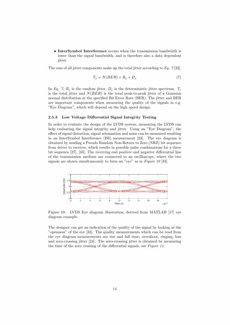
In order to evaluate the design of the LVDS system, measuring the LVDS canhelp evaluating the signal integrity and jitter. Using an ”Eye Diagram”, theeffect of signal distortion, signal attenuation and noise can be measured resultingin an InterSymbol Interference (ISI) measurement [33]. The eye diagram isobtained by sending a Pseudo Random Non-Return to Zero (NRZ) bit sequencefrom driver to receiver, which results in possible pulse combinations for a threebit sequence [27], [33]. The receiving end positive and negative differential lineof the transmission medium are connected to an oscilloscope, where the twosignals are shown simultaneously to form an ”eye” as in Figure 10 [33].
Figure 10: LVDS Eye diagram illustration, derived from MATLAB [17] eyediagram example.
The designer can get an indication of the quality of the signal by looking at the”openness” of the eye [33]. The quality measurements which can be read fromthe eye diagram measurements are rise and fall time, overshoot, ringing, lossand zero-crossing jitter [24]. The zero-crossing jitter is obtained by measuringthe time of the zero crossing of the differential signals, see Figure 11.
14

Figure 11: LVDS Eye diagram illustration with zero-crossing measurement,derived from MATLAB [17] eye diagram example.
The eye itself is composed by superimposing the voltage levels of a transmittedLVDS 1 and 0, transitions between 0 and 1 (i.e. rise and fall time) and bothtransition sequences ”0-1-0” and ”1-0-1” in order to retrieve the minimum 1 or0 time [34].
2.6 Power-over-Ethernet and Power-over-Coaxial
Power-over-Coaxial (PoC) and Power-over-Ethernet (PoE) are two solutions totransfer power over the same cable as the data transfer. The techniques for bothPoC and PoE are similar, however the transfer medium differ, where PoC refersto coaxial cable and PoE refers to a twisted pair type cable [16], [35]. Here on,PoC will denote the concept of transferring power over the same medium asdata using the technology described in this section.
The basic concept is to transfer the power in a frequency band which will notaffect the data signals, and use filters on sender and receiver side to separatepower and data signals. The filter needs to have a high enough input impedanceto not create a stub or introduce reflection for the high speed signals [16]. Often,direct current with ideally no alternating current components will be used forthe power transfer, making a capacitor as a DC-block sufficient to isolate thedata signal input/outputs from the DC [16]. To further isolate power from thedata signal, a series inductance is placed on the connection between the powerand signal. An illustration of such a power transfer schematic is shown in Figure12.
Figure 12: Illustration of a PoC schematic.
The inductance on each side of the cable are denoted as the PoC-filter, and the
15

efficiency and reliability of the system is dependent on the design of the filter.The filter often consists of a combination of inductors and ferrite beads. Thecapacitor which blocks DC voltage on the input of the SerDes has to be in theorder of magnitude such that it lets the front- and back-channel signals throughbut efficiently blocks DC.The capacitor shown in Figure 12 is needed either if PoC is used or not, to blockany direct currents induced in the cable by EMI. The non-idealistic propertiesof the capacitor can be neglected when calculating the capacitor value if a smallpackage ceramic capacitor is used, since the parasitic effect is comparativelysmall at the frequencies of interest [36]. The value of the capacitor is oftengiven by the IC manufacturers as a recommended value.
The parasitic capacitance in the inductor can however not be neglected whendesigning a PoC filter for 3 Gbps, due to the wide spectrum of the combinedfront-and back-channel. The parasitic capacitance will introduce an unwantedlow impedance after the SRF according to Eq. 6.
A rule of thumb when designing a PoC filter is to have 20 times the char-acteristic impedance of the trace in the filter for the affected frequencies toreduce the impact of the stub and reduce the added input reflection, since aT-coupling is made and the load impedance changes, according to Eq. 1 [36].The inductor components, shown in Figure 12, must therefore be chosen sothat the inductance is high enough to block the back channel and have a highenough self resonant frequency to still be high impedance for the front channel.One solution to solve this is to use two inductors in series, one which have ahigh impedance for the back channel frequencies and another that have highimpedance for the front channel frequencies [36]. Depending on the bandwidthand center frequency of the front- and back-channel, ferrite beads can be moresuited to use compared to inductors.
2.7 Cables and Electromagnetic Aspects
In the following sections some common types of cables and shielding are pre-sented along with their individual EMC aspects and design.
2.7.1 Cable Shielding
There are many types of cables, with and without added shields, catering awide area of operation. Even though the range of cables is wide, most of thecables share common design aspects regarding the shielding elements. In thefollowing section, the most common type of shields are presented. The two maintype of shields are the braided shield and the foil shield (also called tape shield)[37],[38], [39], presented in Section 2.7.1.1 and Section 2.7.1.2.
Different kinds of shields have unique properties, making them suitable forshielding for different kind of EMI (also refereed to as noise in the followingsections). In general, a combination of the shields are desirable to get a goodcoverage in all aspects. However, depending on the application and environ-ment where the cable is used, the type of shielding (possible no shielding) thatis required varies. [40], [41].
16

The ideal wire shield can be modeled as a conductor enclosed inside a per-fect solid tubular shield without any holes and gaps as seen in Figure 13 [41].The performance of the shield is directly related to the Skin Effect, thicknessand conductivity [40]. The skin effect is the phenomena where the current in aconductor gathers in the edges of the conductor when the frequency increase.The thickness of the skin is refereed to as Skin Depth and is the thickness of theskin measured from the outer edge of the conductor towards the center [30].
Figure 13: Illustration of an solid tubular shield.
A tubular shield is often not practical for cables other than permanent staticinstallations as the flexibility in the cable is poor[40].
2.7.1.1 Braided Shield
The braided shield is a woven cylindrical shield with either single or multi-wirebraids. The braided shield is mainly efficient in protecting against low frequencyEMI and provides a low DC resistance related to the gauge of the wire used inthe braid [41], [38]. The quality of the braided shield is specified by the percent-age of coverage it provides, where 100 percent coverage is impossible to achievedue to the holes between the weave as seen in Figure 14. Furthermore, thecoverage relates to the size of the holes in the braid, which is the limiting factorregarding shielding against higher frequency EMI, as the holes become large incomparison to the wavelength of the noise [40],[41].
Figure 14: Illustration of a braided shield and the holes in its coverage.
17

The braided shield is typically effective in the range between 30 - 500 MHz,where a coverage above 85 percent is often needed to shield above 100 MHz[40]. The coverage is related to the weaving technique and the gauge of thewires used in the weave.At high frequencies the braided shield also suffer in performance due to the skineffect confining the high frequency currents to the edges of the braid. The totalarea of the braid therefore relates directly to the maximum effective frequencyit can shield against, where greater total surface area provides better shieldingagainst higher frequencies.
2.7.1.2 Foiled Shield
The foiled shield consist of a thin conductive foil, often made of aluminum,that is laminated with a plastic tape to add tensile strength to the shield. It ismainly used to shield against high frequency EMI as it can provide a near fullcoverage without holes in contrast to the braided shield. It is mostly effectiveagainst capacitive coupled noise as the thin foil is easily saturated by the energyin magnetically induced EMI [40].
The foiled shield is not able to fully provide the solid tubular coverage aroundthe wire as in the ideal case due to the overlap in the foil. The foil can beeither longitudinally wrapped around the cable as seen in Figure 15 or helicallywrapped, spiraling around the wires. The thickness of the conductive foil andthe plastic laminate vary depending on the required flexibility and shield prop-erties needed from the cable. There is a trade off between cable thickness andshield effectiveness, where increased insulation (and better dielectric constantof the insulation) improve the cable performance, while reducing the flexibilityof the shielded cable [41],[40]. The impact on the cable performance is furtherdiscussed in Section 2.7.1.3. The foiled shield, in contrast to the braided shield,always need to include an uninsulated conductor called Drain Wire in directelectrical contact to the conductive foil as illustrated in Figure 15.
Figure 15: Illustration of a cable with a foiled shield, including drain wire andfoil overlap.
The drain wire is used in order to terminate the shield in the end of the
18

cables[41]. The foiled shield can in some cases include more than one con-ductive layers and in some cases also an adhesive layer for bonding with othercable components. Closer bonding of the shield and other cable components, aswell as more than one layer, improve the performance of the shield [40].
2.7.1.3 Shielding Effectiveness and Signal Attenuation
An important factor from an EMC perspective regarding shields is the ShieldingEffectiveness. The effectiveness of the shield may be viewed as a ratio betweenthe electrical field induced or radiated on to the shield barrier and the electricalfield that is transmitted through the shield.
An simplified way to describe shielding effectiveness is in terms of ReflectionLoss and Absorption Loss. For the following simplified method to be valid, it isassumed that the skin depth in the conductor is much smaller than the actualthickness of the conductor. The EMI is considered to be far away (far-field) fromthe shield. Moreover the intrinsic impedance in the conductor (which could befurther simplified as the resistance of the conductor) is much smaller than thatof ”free space” i.e. a ”good” conductor [30]. The simplified equation for deter-mine shield effectiveness under the previously states assumptions is given as Eq.8 [30] where η0 is the free space intrinsic impedance, η the conductor impedanceand t
δ is the ratio between the conductor thickness and skin depth.
SEdB = 20log10(η0
4 ∗ η) + 20log10(et/δ) = RdB +AdB (8)
The equation above is divided into the two terms RdB (reflection loss) and AdB
(absorption loss). The reflection loss term is the incoming noise that is reflectedand relates to 1
η , resulting in the conductor impedance being proportional tothe reflection of incoming noise. This could be further simplified and expressedas the lower the DC resistance of the conductor, the better it is at reflectingthe EMI [30],[41]. The absorption loss is the amount of noise absorbed by theshield. It related to t
δ resulting in that the thicker the conductor is the betterthe absorption of the incoming EMI will be.
Comparing the braided and foiled shield using the result of Eq. 8, the braidedshield seems superior to the foiled shield. This as the commonly thicker braidedshield (due to the thickness of the wire) not only give a better shielding againstmagnetically induced noise, but also theoretically is better in terms of reflec-tion and absorption loss due to its low resistance and thickness. However, forthe result to be valid, the shields must be considered waterproof. The braidedshield does not provide a full coverage and thus can only be considered beingwaterproof at relative low frequencies where the wave length is large comparedto the size in the braid gaps. The foiled shield, often composed of a very thinconductive layer still thick enough to enable the use of the simplified methodat high frequencies, have worse performance compared to the braided shield.However, the coverage of the foiled shield could be considered waterproof at allfrequencies and the shield is therefore much more capable at shielding againsthigh frequency noise, even if having a simplified SEdB that is lower than that ofthe braided shield. The two types of shield are often combined as a dual shieldwhere the advantages of a thick and low resistance shield is combined with a
19

full coverage shield, providing a better shield than the two shields separately.
Signal attenuation is the loss in signal strength that occur due to the cableproperties, typically in form of DC resistance and the characteristic impedanceof the cable. The impedance of the conductor increases with a factor propor-tional to the square root of the frequency, due to the skin effect in the conductor.The signal attenuation directly affects the possible length of a cable at differentfrequencies. The attenuation of a cable is often given by the manufacturer at aspecific frequency, where the attenuation is considered to change according toEq. 9, where ℓ is the length for which the attenuation is given [30].
α =powerloss[dB]
ℓ[
dB
length] (9)
The isolation material used in a cables (between wires and shield) is one ofthe main factors that affect the attenuation of the cable, due to the dielectricconstant of the material [41]. This is due to the material contribution to theparasitic capacitance built up between the wires, and wire and shield. Theparasitic capacitance of a cable can be modeled together with the inductance ofthe cable as a low pass filter as seen in Figure 16.
Figure 16: Illustration of parasitic capacitance and inductance of a shieldedwire.
The SRF of the low pass filter seen in Figure 16 can be modelled by Eq. 6,where an increase in either L or C result in a lower SRF, thus resulting in moresignal attenuation at higher frequencies.
2.7.2 Cables
In the scope of this thesis, mainly two types of cables were of interest duethe specifications of the application, namely coaxial and Shielded Twisted Pair(STP) cables. The above mentioned cable types, together with a version of thetwisted pair cable called Shielded Twisted Quad (STQ), are presented in thefollowing subsections.
2.7.2.1 Twisted Pair
Twisted pair cables consists of a wire pair twisted around each other along thelength of the cable. This result in a electrical balance between the pair thatresult in good immunity to noise as well as reducing the radiated emissionsfrom the cable. A good electrical balance implies that the parasitics between
20

the pair is symmetrical, resulting in the induced noise being equal (common)in both wires [42],[41]. This can be shown by considering the electromagneticfield flowing through each loop, inducing a current in the wire, as shown in Fig-ure 17. Because of the alternating polarity in the loops, the induced currentswill ideally cancel each other [30],[40],[42]. Due to the good immunity againstEMI, the twisted pair topology is well suited for differential applications, wherecommon-mode noise is a less problematic factor [43], [41].
Figure 17: Illustration of induced current in a twisted wire pair.
To improve the performance of the cable and reduce crosstalk due to the capac-itive coupling between the wires, the pair should be balanced in the terminationof the cable, meaning that the termination impedance is matched for the pair.If the termination of the pair is not balanced, the wire pairs will start to in-terfere with each other in the near-end-crosstalk (the edges of the cables) dueto unbalance. When a balanced termination is used the near-end-crosstalk isno longer a problem and the performance is limited due to the output sourcesshunt capacitance[40],[41].The Shielded Twisted Pair cable is a twisted pair cable with an added outershield for improved EMI immunity. For a STP cable, the attenuation for highspeed signals is approximated by Eq.10, where R is the resistance due to theskin effect of the wire pair, C the mutual capacitance and L the inductance, allgiven in per unit length in kilometer [40].
α = 14.24 ∗R ∗
√
C
L(10)
When adding a shield to the twisted pair, the capacitance is increased due tothe capacitive coupling between the wires and the shield [44],[40]. Effectively,the addition of a shield around the twisted pair result in an increased attenu-ation in the cable, while providing improved EMC properties as it reduces thesusceptibility of the cable and the radiated noise.
21

2.7.2.2 Shielded Twisted Quad
While the STP cable include a single twisted pair, it is common for cables toinclude more than one twisted pair, e.g. CAT5 ethernet cable consisting of fourwire pairs, shielded or unshielded. The Shielded Twisted Quad cable is designedin a different way from the twisted pair cable. It consists of four wires that, in-stead of being twisted in pairs, is symmetrically arranged and spiraled togetheraround a core. This is commonly refereed to as a star-quad topology, shown inFigure 18 [45],[46].
Figure 18: Illustration of a star-quad cable and the cable cross-section.
The idea behind the star-quad topology is to solve the problem of the twistedwire pairs not being on an exactly equal distance from the noise source. Theresult of the inaccuracy is an error in the approximation that both wires expe-rience the same induced noise as assumed in the case of the twisted pair. Theerror become smaller as the cables is twisted tighter to each other, where thebest position would be having both cables placed at the same position in space.By the arrangement of the wire pairs in the star-quad cable, where in Figure 18the pairs are marked as 1 and 2, the geometrical centers of each pair align asseen in Figure 19 [45],[47].
By aligning the geometrical centers of the differential wire pairs, the inducednoise in the pairs will be equal in both pairs independent on the location ofthe noise source. Furthermore, the STQ cable topology is also providing ahigh resistance to crosstalk between the wires in the pairs. This as the otherpair acts as a ”virtual ground plane” placed between the other pair [45],[47].The STQ resistance to crosstalk and aligned geometrical centers results in goodEMC properties, especially regarding susceptibility as the cable provide goodresistance against EMI when operated in a balanced connection in pairs.
2.7.2.3 Coaxial cables
The coaxial cable is a double conductor cable used in high speed systems suchas radio and video systems. It provides a reliable cable impedance, large band-width and low attenuation [48],[49]. The typical design of the coaxial cable
22

Figure 19: Illustration of a the geometrical centers between the two differentialpairs in the star-quad arrangement.
consists of a conductor core, an insulator and one or more shields, as seen inFigure 20, where the shield act as both a shielding element and as a secondconductor in the cable [50],[48],[49].
Figure 20: Illustration of the design of a coaxial cable.
The typical coaxial cable design is close to the previously mentioned idealshielded wire design, with a conductor inside a concentric cylinder. Theoreti-cally there is no radiated field from the cable as the electric field is containedwithin the conductors, and no electrical noise induced into the cable as theouter conductor act as a tubular shield. Due to the previously discussed imper-fections in different type of shields, the actual EMC properties are not ideal,but generally good [49]. The impedance of the coaxial cable mainly depend onthe diameter of the two conductors and the dielectric constant of the insulationbetween them. Due to this, the process of keeping an even impedance over thefull length of the cable becomes simplified [51],[52].
Two common impedances used in coax cables are the 50 Ω and 75 Ω, where
23

the choice of impedance is a trade off between cable attenuation (high frequen-cies signals) and power handling. Around 75 Ω the attenuation is the lowestfor the cable, while around 30 Ω the power transfer is best, making the 50 Ωimpedance a trade of between both attenuation and power transfer [52].
Similar to the cables and shields previously described, the capacitive couplingbetween the conductors have a great impact on the bandwidth of the cable,where a low capacitance is desired for high speed applications [50].
24

3 Implementation
In order to realize the system described in Section 2.1, a market survey wasconducted to investigate existing and coming SerDes solutions. The results ofthe market survey was used to choose one suitable solution which would bemanufactured and tested in order to answer the second problem formulation.The process of choosing a solution, designing and testing the chosen solutionwill be described in this section.
3.1 SerDes Market Survey
To get a clear view of available solutions, a document which compares specifi-cations, price and functionality was made. This document was the compilationof the market survey conducted in the early stage of the thesis.The initial phase of the survey consisted of searching IC manufacturers and com-ponent distributors websites for keywords, as well as investigating the in-houseexperience at Autoliv for similar systems. Autoliv had some initial suggestionson possible solutions and manufacturers they wanted to investigate further. Thisinitial information was used as ground base for the survey in terms of searchterms and specifications. Based on the search results, attempts to gather fur-ther information about possible solutions were made by directly contacting themanufactures, requesting more detailed information.If a NDA was required to obtain further information, an attempt was madeto establish a NDA between Autoliv and that manufacturer. However, as thelegal procedure involved in signing NDAs were complicated, no effort were putbeyond offering a standard NDA. If the NDA could not be agreed upon, nofurther attempts were made in the time frame of this thesis. For manufacturersthat currently had an active NDA with Autoliv, contact were made directly toeither sales representative or application engineer at said manufacturer.
The number of chip manufacturers producing SerDes solutions with MIPI CSI-2 interface was limited to a few with one or two solution compliant with therequired data throughput. This pivoted the market survey into looking closerat system solutions rather than a great number of solutions.
The importance of different specification varied due to the different solutionsnot being equal in their construction, which made a direct comparison infeasibleto some extent. E.g. some SerDes ICs needed complementary ICs, which madea direct comparison between such a solution and a ”one-chip” solution unfair.The different system solutions were therefore compared at a system level to de-termine the best system solution for the task at hand.When the survey was completed with regards to manufacturers and ICs, the dif-ferent system solutions were compared to each other in regards to the followingspecifications:
• Total System Cost
• Compliance with the specification and limitations in Section 1.3 and Sec-tion 1.4
• Serial Link Speed
25

• Control Channel Compatibility
• Availability
• Overall Compliance with the rest of the system, i.e. compatibility with thecamera, video processor, MIPI CSI-2 and control signals without alteringany existing hardware
• Specific Features, will depend on the IC(s)
• Approximated system complexity
The comparative specifications served as the basis for the decision of whichSerDes solution that was to be used in the design, to be further evaluated andused as a demonstration for Autolivs customers. Due to NDAs with some ofthe IC manufacturers, the disclosed market survey will have modified values sothat the NDA is respected. The modification will however be made so that theresults are comparative. When a value modification is not possible, the featurewill not be disclosed in this report, but the overall result will be described. Theresults of the market survey is shown in Section 4, however the choice of ICaffected the design and the IC used in this thesis will therefore be disclosed inthis section.
3.2 Choice of SerDes Integrated Circuits
The choice of the SerDes ICs were made together with Autoliv, where the firstpriority was compliance with existing and future systems. The basis of the de-cision was the market survey described in the previous section, however Autolivrequested to be a part of the decision process.Based on the survey, two different solutions from two different manufacturerswere chosen as the best candidates for implementation. The two different so-lutions both complied with the block diagram shown in Figure 21 and Figure22, depicting the system built and tested in the scope of this thesis. Since bothmanufacturer’s ICs complied with the same block diagram, a direct comparisonwas possible.Since this thesis focused on the performance and implementation of the systems,some additional elements such as microcontroller and multiple high speed con-nectors were a part of the design. These components were necessary to performthe functionality validation and performance tests, and would not normally bea part of an end-product to be sold to a customer.
26

Figure 21: Extended system overview of the SerDes system, serializer side.
Figure 22: Extended system overview of the SerDes system, deserializer side.
27

The choice of which of the two solutions to implement were then a matter ofdirect comparison of different ICs specification and their compliance with thecurrent camera and VP. The final deciding factor were the number of availableGeneral Purpose Input/Output (GPIO), due to the number of control- and test-signals needed between the camera and the VP.In reference to Section 4.1, Manufacturer 1 (M1, protected by NDA) had moreGPIOs than Texas Instruments (TI) which lead to the choice of M1 as the ICsolution for this thesis, since the number of control signals determined the min-imum number of GPIOs.
However, notable is that the ICs from Texas Instruments comply with thelimitations and specification of the system. In order to address the need foradditional GPIOs, additional hardware and software would be needed in theSerDes solution to not force a re-design of the VP- and camera-modules. Theadded complexity further supported the choice of the SerDes solution providedby M1.When the M1 ’s SerDes ICs were chosen, a system had to be designed using saidICs, described in the following sections.
3.3 System Design
A system overview in shape of a block diagram for the M1 solution had alreadybeen designed, see Figure 21 and Figure 22, since it was needed in the decisionprocess. The remaining design of the individual blocks shown in Figure 21 andFigure 22, also stated below, were designed to support the chosen SerDes ICs.
• Serializer and Deserializer IC
• High Speed Connector
• High Speed Data and Power Cable
• Power-over-Coaxial Filter
• Power Management
• Microcontroller (MCU)
These subsystems are described in further detail in the following sections.
3.3.1 Serializer and Deserializer Integrated Circuits
The serializer and deserializer ICs chosen from M1 featured, among others spec-ifications presented in Section 4.1, support for a full four-lane MIPI CSI-2 in-terface. The ICs also featured several link speeds modes, here from divide into,and refered to as Low speed mode and High speed mode for future reference.Furthermore, support for both coaxial and STP cables was available for useas the high speed serial link connection medium. In order to evaluate the fullcapabilities in the serial link, the SerDes designs were implemented with theoption to use both coaxial and STP interface.
Due to limitations in the performance, as well as availability of connectors forSTP cables suitable for high frequency operations, a STQ cable and connector
28
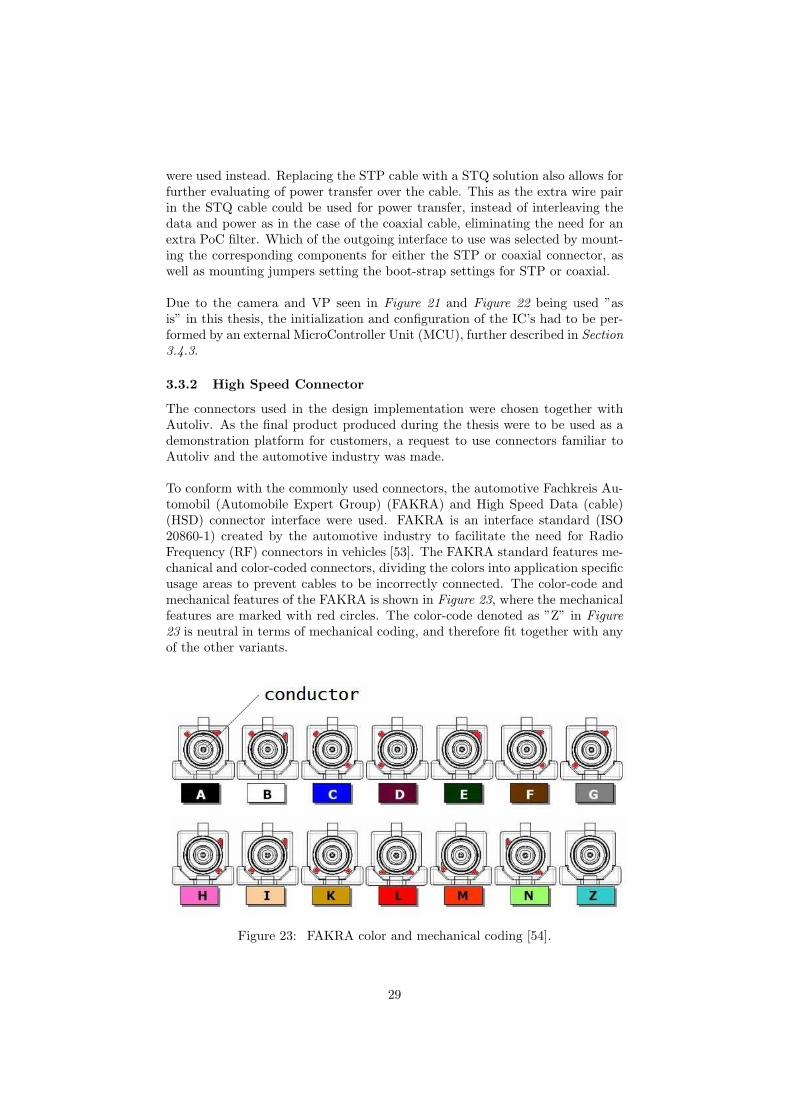
were used instead. Replacing the STP cable with a STQ solution also allows forfurther evaluating of power transfer over the cable. This as the extra wire pairin the STQ cable could be used for power transfer, instead of interleaving thedata and power as in the case of the coaxial cable, eliminating the need for anextra PoC filter. Which of the outgoing interface to use was selected by mount-ing the corresponding components for either the STP or coaxial connector, aswell as mounting jumpers setting the boot-strap settings for STP or coaxial.
Due to the camera and VP seen in Figure 21 and Figure 22 being used ”asis” in this thesis, the initialization and configuration of the IC’s had to be per-formed by an external MicroController Unit (MCU), further described in Section3.4.3.
3.3.2 High Speed Connector
The connectors used in the design implementation were chosen together withAutoliv. As the final product produced during the thesis were to be used as ademonstration platform for customers, a request to use connectors familiar toAutoliv and the automotive industry was made.
To conform with the commonly used connectors, the automotive Fachkreis Au-tomobil (Automobile Expert Group) (FAKRA) and High Speed Data (cable)(HSD) connector interface were used. FAKRA is an interface standard (ISO20860-1) created by the automotive industry to facilitate the need for RadioFrequency (RF) connectors in vehicles [53]. The FAKRA standard features me-chanical and color-coded connectors, dividing the colors into application specificusage areas to prevent cables to be incorrectly connected. The color-code andmechanical features of the FAKRA is shown in Figure 23, where the mechanicalfeatures are marked with red circles. The color-code denoted as ”Z” in Figure23 is neutral in terms of mechanical coding, and therefore fit together with anyof the other variants.
Figure 23: FAKRA color and mechanical coding [54].
29
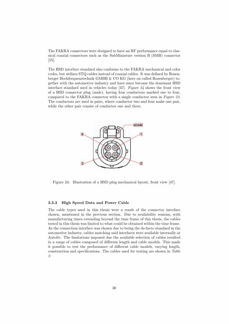
The FAKRA connectors were designed to have an RF performance equal to clas-sical coaxial connectors such as the SubMiniature version B (SMB) connector[55].
The HSD interface standard also conforms to the FAKRA mechanical and colorcodes, but utilizes STQ cables instead of coaxial cables. It was defined by Rosen-berger Hochfrequenstechnik GMBH & CO KG (here on called Rosenberger) to-gether with the automotive industry and have since become the dominant HSDinterface standard used in vehicles today [47]. Figure 24 shows the front viewof a HSD connector plug (male), having four conductors marked one to four,compared to the FAKRA connector with a single conductor seen in Figure 23.The conductors are used in pairs, where conductor two and four make one pair,while the other pair consist of conductor one and three.
Figure 24: Illustration of a HSD plug mechanical layout, front view [47].
3.3.3 High Speed Data and Power Cable
The cable types used in this thesis were a result of the connector interfacechosen, mentioned in the previous section. Due to availability reasons, withmanufacturing times extending beyond the time frame of this thesis, the cablestested in this thesis was limited to what could be obtained within the time frame.As the connection interface was chosen due to being the de-facto standard in theautomotive industry, cables matching said interfaces were available internally atAutoliv. The limitations imposed due the available selection of cables resultedin a range of cables composed of different length and cable models. This madeit possible to test the performance of different cable models, varying length,construction and specifications. The cables used for testing are shown in Table2.
30

Table 2: Type of cables tested and available length(s)
Connection Cable Length(s)Interface
STQ LEONI Dacar 535-2 [62] 10 m
STQ LEONI Dacar 538 [63] 5 m
Coax LEONI Dacar 462 [64] 5 m, 10 m (2×5 m)
Coax Gebauer & Griller (G&G) 5 m, 10 mKoax-B(105)-50-2,1-3,3 [65]
Coax Coleman Cable Inc (CCI) 2 m991069-xx-08 [66]
The cables differ from each other in terms of performance, construction andshielding. The specifications that were of main interests for the application areshown in Table 3 and Table 4, where the data was obtained from the cables’datasheets. The frequency for which the attenuation is presented were chosensuch that all cables within one type have recorded data. The shield types isgiven in order of appearance seen from cable center, and include the constructionmaterial. All STQ cables are specified with a differential impedance at 100 Ω,while all coaxial cables are specified with a 50 Ω impedance.
Table 3: Specifications of STQ cables tested
Cable LEONI Dacar 535-2 LEONI Dacar 538
Attenuation [dB/m] 1.24 @ 1 GHz 1.24 @ 1 GHz
Shield Type(s) PETP/Al Foil Ti-Cu Braid& Ti-Cu Braid & PVC/Al Foil
Shield Coverage 100% & 92% ≥92% & 100%
Shielding Effectiveness ≥40 dB @ 1 GHz ≥40 dB @ 1 GHz
Insulation Polypropylene (PP) Polypropylene (PP)
Diameter [mm] 4.6 4.6
The two STQ cables tested were from the same manufacturer, and shared almostidentical specifications. This was due to the Dacar 535 being the successor ofthe Dacar 538 cable, where the ”-2” addition to Dacar 535 implies it being thenon-stationary version of Dacar 535. The difference between the non-stationaryversion and original version of the cable was a filler placed in the cable center,as seen in Figure 25. The purpose of the filler was to reduce the displacementand alignment errors between the wire pairs, which could arise from the cablebeing regularly moved or bent.
31

Figure 25: Cross-section of a STQ cable, with and without filler.
Both cables was build with a Tinned Copper (Ti-Cu) Braid with a visual cov-erage of at least 90% and a Aluminum (Al) foil with 100% visual coverage.The foil shield differed in terms of the plastic used for the foil, where PolyvinylChloride (PVC) was used in the Dacar 538 foil, and Polyethylene terephthalate(PETP) was used in the Dacar 535-2 foil.
Table 4: Specifications of coaxial cables tested
Cable LEONI Dacar 462 G&G Koax-B(105) CCI 991069-xx-08-50-2,1-3,3
Attenuation 2.38 @ 6 GHz 1.72 @ 5.6 GHz 0.99 @ 1 GHz[dB/m] (0.88 @ 1 GHz) (1.8 @ 6 GHz
calculated, and0.6 @ 1 GHz )
Shield Type(s) Al/PETP/Al Foil Al/PETP/Al Foil Ti-Cu Braid& Ti-Cu Braid & Ti-Cu Braid
Shield Coverage 100% & 80% 100% & 90% 88%
Shielding No Data ≥90 dB @ 1 GHz No DataEffectiveness
Dielectric Cross-linked PP Polyethylene (PE)polyethylene (XPE)
Capacitance Max 106 Max 94 Nominal 101[pF/m]
Conductor 317 52 No DataResistance[Ohm/km]
Diameter [mm] 2.8 3.3 2.5
The three coaxial cables tested differed from each other in many of the statedspecifications, where the shield types were the only factor shared by the G&Gand Dacar cable, while the CCI cable only had a single braided shield. Theattenuation given in Table 4 is given for the highest frequency specified in thedatasheets available for each cable. For comparison reasons, attenuation for theG&G and Dacar cable is also given at 1 GHz, as it is the maximum given valuefor the CCI cable. Furthermore, the 6 GHz attenuation for the G&G cable is
32

calculated using the formula provided within the datasheet to further supportthe comparison between it and the Dacar 462 cable.
The cable from G&G had a specified attenuation of approximately 25 per-cent less then the Dacar cable (using the calculated attenuation at 6 GHz) andbetter shield coverage. This makes it a theoretically better cable in terms ofsignal integrity and EMI. At 1 GHz, the G&G cable performed better in termsof attenuation than that of the Dacar, with almost an 32 percent difference inattenuation. The CCI cable had the worst performance seen in regards to at-tenuation with an attenuation approximately 40 percent higher than the G&Gcable, and 11 percent higher than the Dacar cable. Due to the CCI cable onlyhaving a braided shield, it can be assumed to have significantly worse perfor-mance at higher frequencies, where the foil shield is most efficient, as discussedin Section 2.7.1.2.
The difference in capacitance per meter and conductor resistance per kilometerwould affect the attenuation of the cables. The G&G cable, specified with lowervalues in both categories, should therefore provide less attenuation at higherfrequencies, as supported by the specified attenuation in Table 4. These valuesare affected, among other things, by the type of dielectric and materials in thecore and shield of the cable.
For the Dacar and CCI cables, no value for shielding effectiveness was givenin the datasheet. However, an assumption based on section 2.7.1.3 was made,where the shielding effectiveness was assumed to be less than that of the G&Gcable, based on the Dacar and CCI cable, having either or both, higher conduc-tor resistance and a copper braid with less coverage than that of the G&G cable.
3.3.4 Power over Coaxial Filter
The design of the Power-over-Coaxial (PoC) filter used together with the coaxialcable interface in order to interleave the power and data transfer was done intwo different implementations. A reference design was used together with an al-ternative design in order to be able to compare performance and price of the twosolutions. The reference design was provided by M1 together with simulationson the filter performance. Using the provided filter simulations, the alternativefilter was designed by the authors (of this report) with the goal of reducing thecomponent count, over all size and price of the final filter.
The author filter design was made by surveying websites of manufacturers offerrite beads and inductors. The filter was supposed to block both the front-and back-channels, therefore a band-stop type filter needed to be designed forpower transfer, where the series capacitance was the parasitic capacitance of theinductors and ferrite beads, see Section 2.6. The PoC filter given by M1 wassimulated in ADS [6] and using data from the inductor and ferrite bead manu-facturers, equivalent circuits were used to model the ferrite beads and inductors.
Simulations of the given PoC-filter were done in order to compare the author’sdesign to a supposedly working filter. The author’s filter designs equivalent
33
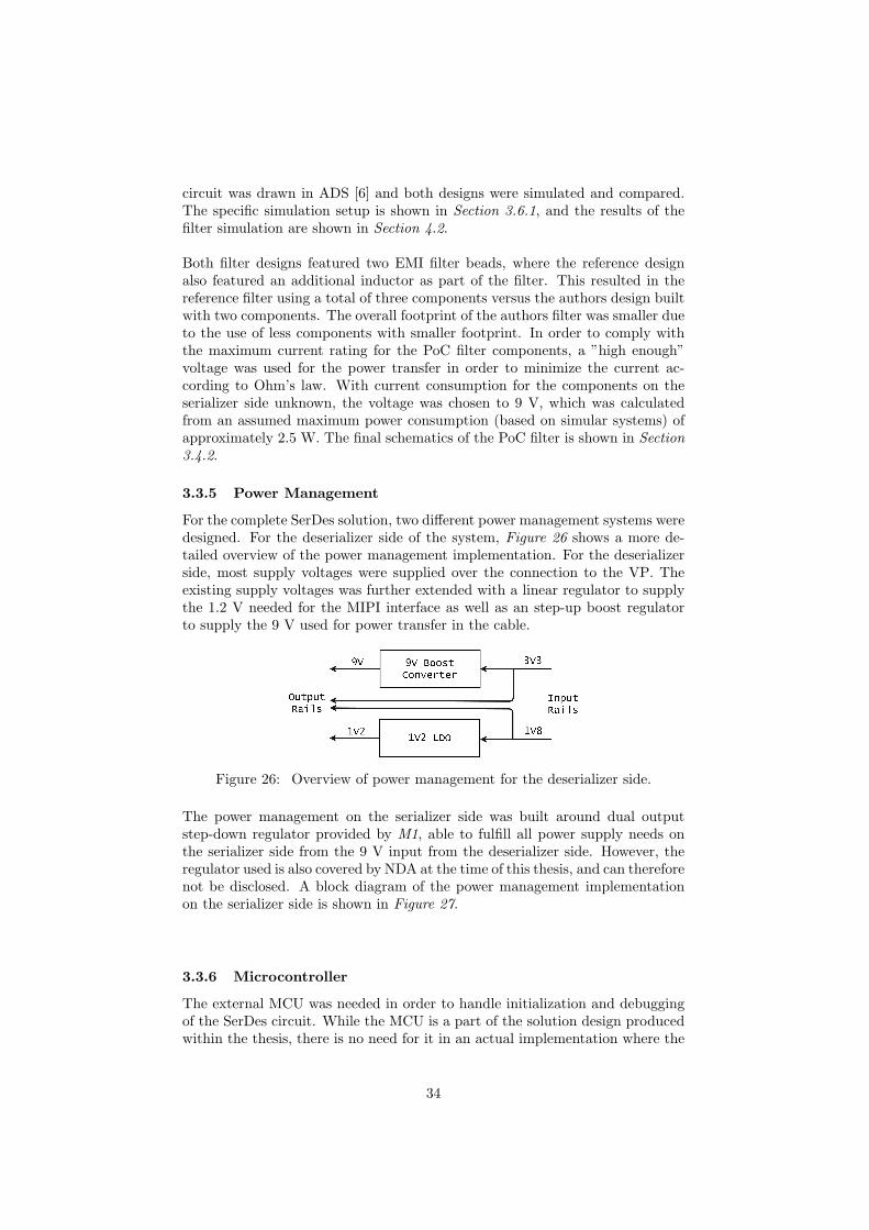
circuit was drawn in ADS [6] and both designs were simulated and compared.The specific simulation setup is shown in Section 3.6.1, and the results of thefilter simulation are shown in Section 4.2.
Both filter designs featured two EMI filter beads, where the reference designalso featured an additional inductor as part of the filter. This resulted in thereference filter using a total of three components versus the authors design builtwith two components. The overall footprint of the authors filter was smaller dueto the use of less components with smaller footprint. In order to comply withthe maximum current rating for the PoC filter components, a ”high enough”voltage was used for the power transfer in order to minimize the current ac-cording to Ohm’s law. With current consumption for the components on theserializer side unknown, the voltage was chosen to 9 V, which was calculatedfrom an assumed maximum power consumption (based on simular systems) ofapproximately 2.5 W. The final schematics of the PoC filter is shown in Section3.4.2.
3.3.5 Power Management
For the complete SerDes solution, two different power management systems weredesigned. For the deserializer side of the system, Figure 26 shows a more de-tailed overview of the power management implementation. For the deserializerside, most supply voltages were supplied over the connection to the VP. Theexisting supply voltages was further extended with a linear regulator to supplythe 1.2 V needed for the MIPI interface as well as an step-up boost regulatorto supply the 9 V used for power transfer in the cable.
Figure 26: Overview of power management for the deserializer side.
The power management on the serializer side was built around dual outputstep-down regulator provided by M1, able to fulfill all power supply needs onthe serializer side from the 9 V input from the deserializer side. However, theregulator used is also covered by NDA at the time of this thesis, and can thereforenot be disclosed. A block diagram of the power management implementationon the serializer side is shown in Figure 27.
3.3.6 Microcontroller
The external MCU was needed in order to handle initialization and debuggingof the SerDes circuit. While the MCU is a part of the solution design producedwithin the thesis, there is no need for it in an actual implementation where the
34

Figure 27: Overview of power management for the serializer side.
VP can control the SerDes IC’s.
The chosen MCU was STM8AF6223 from STMicroelectronics, which is an au-tomotive classified 8-bit MCU supporting I2C and Universal Asynchronous Re-ceiver/Transmitter (UART), among other peripherals. The addition of the ex-ternal MCU allows for further configuration, monitoring and status readoutof the system while active, using the MCU UART interface to provide statusprintout and configuration possibilities.
3.4 Schematics Design
The schematic designs were based on the block diagrams in Figure 21 and Figure22 where each block’s auxiliary components were determined by their individualdatasheet and reference designs. The goal was to make the design as versatileas possible, in order to facilitate re-configuration and measurements on the fin-ished circuit board.
The possibilities to re-configure the system involved interfaces, PoC-filters andstart-up configuration, and the schematics were designed with this in mind.This was solved by using 0 Ω resistors and 2.54 mm general purpose headers,used as jumpers on the PCB. Headers were also used for accessing the I2C andUART to/from the SerDes IC and MCU as well as measuring current for thesystem and measuring a reference voltage for the camera.
The parts of schematics design that involves the high speed connectors, PoCfilter and MCU are shown in the following sections. The whole SerDes schemat-ics is not shown due to the NDA in effect. However, the schematic parts thatincludes the SerDes ICs were designed based on recommendation provided bythe M1 and the datasheet. The remaining parts of the schematics, presented inthe following sections, were designed by the authors to be able to operate andinterface the main ICs and auxiliary components.
3.4.1 High Speed Connector Schematics
Since two different high speed connectors and cables was to be tested, theschematics were designed with this taken into account. This was done by mount-ing jumpers and resistors associated with either the coaxial or STQ interface.The final procedure for switching interface involved changing two resistors andone jumper. The schematics for the deserializer high speed connectors is shownin Figure 28 and the schematics for the serializer high speed connectors is shownin Figure 29.
35

Figure 28: Deserializer high speed front end connector schematic.
The two leftmost connections in Figure 28 connects to the deserializer IC, fol-lowed by the two capacitors that are always mounted on the PCB independentof the chosen high speed interface. The resistors in the figure decide whichconnector will be used, where mounting only R123 and R124 will result in thecoaxial connector and mounting only R122 and R125 will results in the use ofthe STQ connector. No other combination of resistor mounting is supportedand might result in malfunction.
Figure 29: Serializer high speed front end connector schematic.
As done for the deserializer interface selection, the serializer connector was cho-sen by mounting the specific resistors related to the desired interface. Theleftmost connections in Figure 29 goes to the serializer IC, and the capacitorswill always be mounted.
36

To use the coaxial connector, only resistors R116 and R119 must be installed,while for the STQ connector only resistors R117 and R118 must be installed.As for the deserializer, any combination of these other than the above men-tioned might cause the system to malfunction and is therefore not supported orrecommended.
The AC-coupling capacitors mounted on the input and output of the SerDesfront end provides a DC block in the IC ports, increasing common-mode noiserejection at the input while also protecting against overvoltage and electricalshort scenarios [56].
3.4.2 Power-Over-Coaxial Filter Schematics
The PoC filter design in the serializer and deserializer schematics were donesimilar to each other, both including the reference and custom filter designsmentioned in Section 3.3.4 . The design of the PoC filter for the serializer isshown in Figure 30, while the design for the deserializer is shown in Figure 31.The two schematics differ in regards to the placement of the resistors due to theinput and output of the filter. The filtering components seen in Figure 30 andFigure 31 are ferrite beads (denoted as FB*) and inductors (denoted as L*).
Figure 30: Serializer Power over Coaxial filter schematic.
Figure 31: Deserializer Power over Coaxial filter schematic.
37

The order of the filter components is chosen in such a way that the componentsresponsible for blocking the most high frequency signals are placed closest tothe high speed interface. This was done to minimize the length and impact ofthe stub created due to the filter placement on the high speed trace, see Section2.6. This is seen in as FB102 and FB103 in Figure 30 are placed close to themarked input, while the same components (with the same name) in Figure 31are placed close to the marked output.
The selection of which filter that was used were done by mounting either R139and R140 in Figure 30 on the serializer side. Or the corresponding resistorsR137 and R138 on the deserializer design, seen in Figure 31. This to provideflexibility when evaluation of the two different filter designs was to be per-formed. All component except for the resistors were installed at all time, andby installing R139 (serializer) or R137 (deserializer), the filter designed by theauthors were chosen. If R140 (serializer) or R138 (deserializer), is installed,the filter designed by M1 will be chosen. Installing both resistors in any of thedesigns will result in both filter being active, which is not recommended sincethis will result in an reduced equivalent of the series resistance of the combinedfilters, as well as introduce additional stub elements on the high speed trace,affecting the signal integrity, see Section 2.6.
The OUTPUT in the deserializer PoC design is connected to the coaxial highspeed front end, called ”PWR POCF” in Figure 28. Furthermore, the INPUTin the serializer PoC design is connected to the coaxial high speed-front end,called ”PWR POC IN” in Figure 29. The ability to choose from two differentfilter designs was to evaluate the performance versus footprint factor from afunctionality point of view. The PoC filter was simulated in order to evaluatefunctionality, see Section 3.6.1.
3.4.3 Microcontroller Unit and Level Converter Schematic
The STM8AF6223 microcontroller have a recommended layout, which was fol-lowed as closely as possible. The UART, I2C and programming interface wasconnected to 2.54 mm headers to be easily accessible. The voltage level of theI2C port of the MCU was 3.3 V, while the camera and SerDes ICs operatesat 1.8 V. Therefore, an I2C level converter, which unidirectionally converts thedifferent voltage level I2C’s was implemented into the design. The Texas In-struments TXB0102 level converter was used, and the schematics for the levelconverter was taken from the datasheet of said converter, and pull-up resistorsbetween the MCU and the level converters were added. The schematics for thelevel converter can be seen in Figure 32 and the MCU schematics is shown inFigure 33.
The component named U104 in Figure 33 is the level converter IC, with the re-spective power levels and outputs shown on each side of the IC. The right-mostresistors in Figure 32, R126 and R127 are the I2C pull up resistors.
38
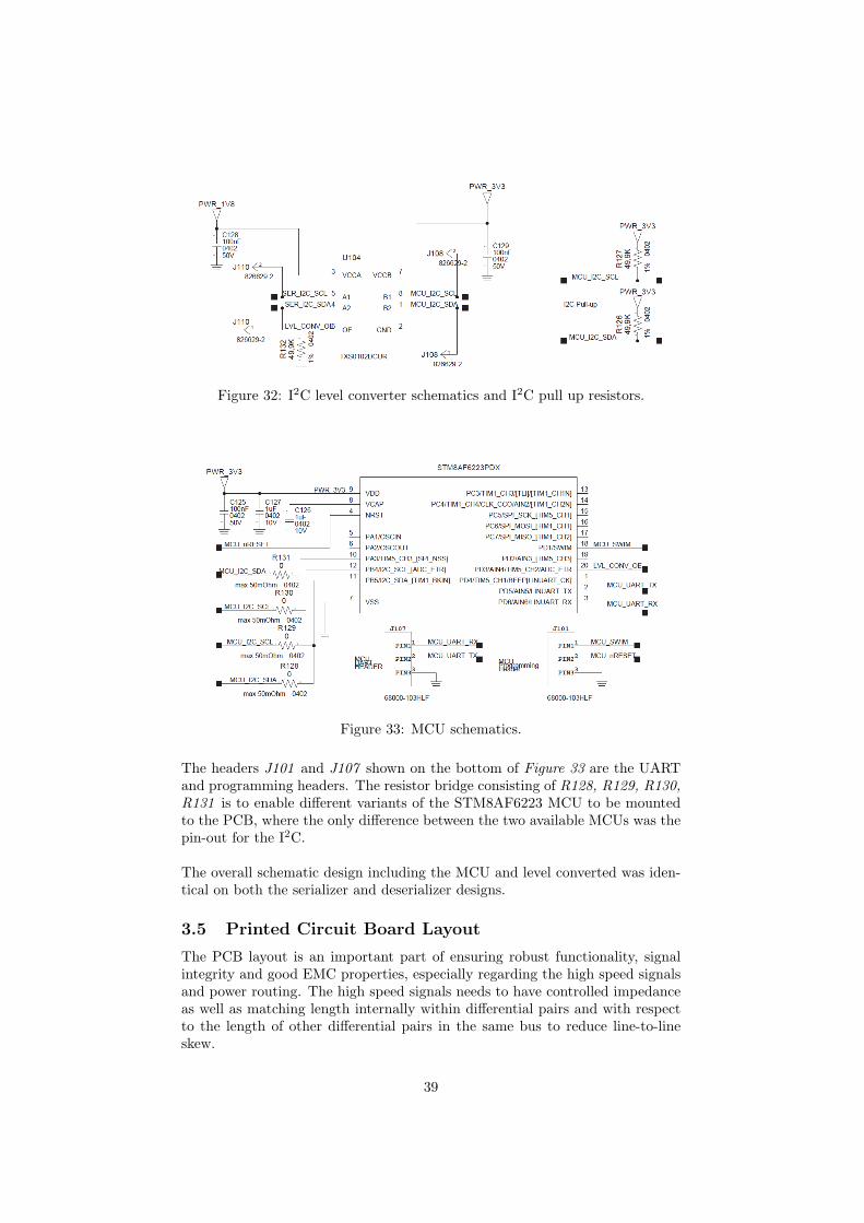
Figure 32: I2C level converter schematics and I2C pull up resistors.
Figure 33: MCU schematics.
The headers J101 and J107 shown on the bottom of Figure 33 are the UARTand programming headers. The resistor bridge consisting of R128, R129, R130,R131 is to enable different variants of the STM8AF6223 MCU to be mountedto the PCB, where the only difference between the two available MCUs was thepin-out for the I2C.
The overall schematic design including the MCU and level converted was iden-tical on both the serializer and deserializer designs.
3.5 Printed Circuit Board Layout
The PCB layout is an important part of ensuring robust functionality, signalintegrity and good EMC properties, especially regarding the high speed signalsand power routing. The high speed signals needs to have controlled impedanceas well as matching length internally within differential pairs and with respectto the length of other differential pairs in the same bus to reduce line-to-lineskew.
39

A four metal layer PCB stack-up were chosen for the PCB design, utilizingthe top and bottom layers for signal routing and the two internal layers aspower planes. Furthermore, the differential and single-ended impedances thathad to be controlled were specified by the authors. A request was then madeto the appointed PCB manufacturer Cogra (Cogra Pro AB, fabriksvagen 1, 44637 Alvangen), where a stack-up suitable for the needed impedance control andtheir processes was requested.
The trace width and spacing for the impedance control was given by manufac-turer and was based on their previous experience regarding impedance controlledtraces and manufacturing of said traces. The stack-up with the calculated tracewidth and spacing done by Cogra is shown in Table 5.
Table 5: Stack-up given by PCB manufacturer for controlled impedance
Layer, thickness 100 Ω trace width/spacing 50 Ω trace width ǫr
Signal, 18 µm w=154 µm, s=170 µm w=220 µm N/A
Pre-preg, 126 µm N/A N/A 3.95
Plane, 35 µm N/A N/A N/A
Core, 1200 µm N/A N/A 4.04
Plane, 35 µm N/A N/A N/A
Pre-preg, 126 µm N/A N/A 3.95
Signal, 18 µm w= 154 µm, s=170 µm w=220 µm N/A
The PCB was designed so that all components were mounted on the primaryside to favor the mounting process, since no space restrictions were implied onthe PCB produced in this thesis due to the system was to be used as a demon-strator. The PCB size was 70x70 mm, and featured silk screen printing ofheader locations to ease setup and installation of the system for demonstrationpurposes.
3.5.1 High Speed Layout Guidelines
The routing of high speed traces had to be done with care in order to reduceeffects which reduces the signal integrity. For the layout of the high speed signalscovered in the following sections, the rules were collected from IC manufacturersapplication documents [57],[58],[59].There is however a great selection of rules, and stating every rule would beproduce a list to long to include in this thesis. Therefore, a selection of ruleswhich were considered most important in the scope of this thesis are statedbelow.
• Do not use right-angle bends, use arcs or curves instead
• For single ended signals, the minimum spacing to other electrical objectsshould be no smaller than 2 times the width of the trace
• For differential signals, the minimum spacing to other electrical objectsshould be no smaller than 2 times the spacing of the differential pair
40
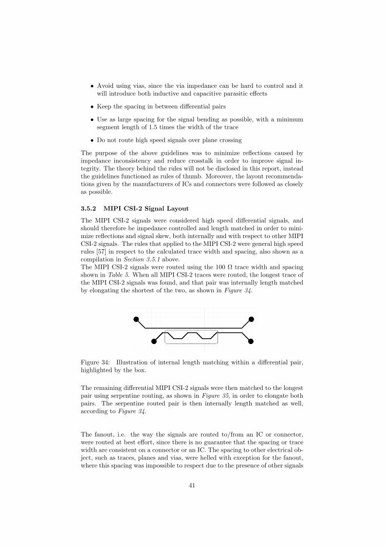
• Avoid using vias, since the via impedance can be hard to control and itwill introduce both inductive and capacitive parasitic effects
• Keep the spacing in between differential pairs
• Use as large spacing for the signal bending as possible, with a minimumsegment length of 1.5 times the width of the trace
• Do not route high speed signals over plane crossing
The purpose of the above guidelines was to minimize reflections caused byimpedance inconsistency and reduce crosstalk in order to improve signal in-tegrity. The theory behind the rules will not be disclosed in this report, insteadthe guidelines functioned as rules of thumb. Moreover, the layout recommenda-tions given by the manufacturers of ICs and connectors were followed as closelyas possible.
3.5.2 MIPI CSI-2 Signal Layout
The MIPI CSI-2 signals were considered high speed differential signals, andshould therefore be impedance controlled and length matched in order to mini-mize reflections and signal skew, both internally and with respect to other MIPICSI-2 signals. The rules that applied to the MIPI CSI-2 were general high speedrules [57] in respect to the calculated trace width and spacing, also shown as acompilation in Section 3.5.1 above.The MIPI CSI-2 signals were routed using the 100 Ω trace width and spacingshown in Table 5. When all MIPI CSI-2 traces were routed, the longest trace ofthe MIPI CSI-2 signals was found, and that pair was internally length matchedby elongating the shortest of the two, as shown in Figure 34.
Figure 34: Illustration of internal length matching within a differential pair,highlighted by the box.
The remaining differential MIPI CSI-2 signals were then matched to the longestpair using serpentine routing, as shown in Figure 35, in order to elongate bothpairs. The serpentine routed pair is then internally length matched as well,according to Figure 34.
The fanout, i.e. the way the signals are routed to/from an IC or connector,were routed at best effort, since there is no guarantee that the spacing or tracewidth are consistent on a connector or an IC. The spacing to other electrical ob-ject, such as traces, planes and vias, were helled with exception for the fanout,where this spacing was impossible to respect due to the presence of other signals
41
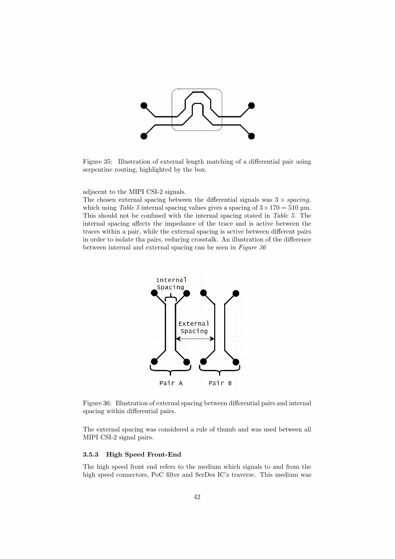
Figure 35: Illustration of external length matching of a differential pair usingserpentine routing, highlighted by the box.
adjacent to the MIPI CSI-2 signals.The chosen external spacing between the differential signals was 3 × spacing,which using Table 5 internal spacing values gives a spacing of 3×170 = 510 µm.This should not be confused with the internal spacing stated in Table 5. Theinternal spacing affects the impedance of the trace and is active between thetraces within a pair, while the external spacing is active between different pairsin order to isolate tha pairs, reducing crosstalk. An illustration of the differencebetween internal and external spacing can be seen in Figure 36
Figure 36: Illustration of external spacing between differential pairs and internalspacing within differential pairs.
The external spacing was considered a rule of thumb and was used between allMIPI CSI-2 signal pairs.
3.5.3 High Speed Front-End
The high speed front end refers to the medium which signals to and from thehigh speed connectors, PoC filter and SerDes IC’s traverse. This medium was
42

the copper traces on the PCB, and not unlike the MIPI CSI-2 signals, these highspeed signals needed special consideration in regards to impedance, length andspacing to other electrical objects. M1 provided specifications for the design ofthe front end, in form of benchmarks regarding signal integrity for which theIC would work. These benchmarks included Insertion Loss, Return Loss andInsertion loss to Return loss Ratio (IRR).The insertion loss was given by S21 for the forward channel and by S12 for thereverse channel. The return loss was given by S11 for the forward channel andby S22 for the reverse channel. The IRR is the ratio between above mentionedparameters, the calculation for which is shown in Eq. 11 and Eq. 12.
IRRFrontChannel =S21
S22
(11)
IRRBackChannel =S12
S11
(12)
Using Eq. 11 and Eq. 12 above, it can be seen that the IRR show the interfer-ence at the forward channel receiver caused by reflected energy from the reversechannel transmitter.The high speed front end layout must fulfill either the insertion loss specifica-tion and return loss specification, or the insertion loss specification and IRRspecification, according to M1. The simulation implementation regarding thecomparison of these parameters are further explained in Section 3.6.2.2.
The use of two different connectors, where the STQ connector have a 100Ω differential impedance and the coaxial connector got a 50 Ω single endedimpedance, induces some more requirements on the characteristic impedance ofthe high speed front-end traces.
Due to the schematic of the front-end, the optimum would be to have a 100Ω differential pair with 50 Ω single ended impedance. To calculate this, Sat-urn PCB Toolkit[7] was used. The calculated dimensions needed to be withinthe manufacturing specifications, but using the example values in Table 5 as astarting point, the desired dimensions would be larger than the given values.The resulting dimensions for the combined 100 Ω differential and 50 Ω singleended dimensions are shown in Table 6. The plating thickness was given as 35µm.Using Saturn PCB Toolkit [7], the impedances for Table 5 and Table 6 werecalculated and the results are shown in Table 7 for a comparison. The differen-tial impedance was calculated using the ”Differential Pairs” tab and the singleended impedance was calculated using the ”Conductor Impedance” tab in Sat-urn PCB Toolkit[7]. The conductor height value in both cases was taken fromthe pre-preg layer in the stack-up shown in both Table 5 and Table 6.When the dimensions were calculated, the high speed front end was routed. Therouting was made so that the copper traces followed high speed routing rule ofthumbs in Section 3.5.1. The routing was also made so that the total lengthwas minimized while still being able to length match the differential pair. The
43
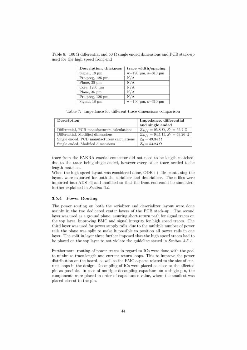
Table 6: 100 Ω differential and 50 Ω single ended dimensions and PCB stack-upused for the high speed front end
Description, thickness trace width/spacing
Signal, 18 µm w=190 µm, s=310 µm
Pre-preg, 126 µm N/A
Plane, 35 µm N/A
Core, 1200 µm N/A
Plane, 35 µm N/A
Pre-preg, 126 µm N/A
Signal, 18 µm w=190 µm, s=310 µm
Table 7: Impedance for different trace dimensions comparison
Description Impedance, differentialand single ended
Differential, PCB manufacturers calculations Zdiff = 95.8 Ω, Z0 = 55.2 Ω
Differential, Modified dimensions Zdiff = 94.1 Ω, Z0 = 49.26 Ω
Single ended, PCB manufacturers calculations Z0 = 49.34 Ω
Single ended, Modified dimensions Z0 = 53.23 Ω
trace from the FAKRA coaxial connector did not need to be length matched,due to the trace being single ended, however every other trace needed to belength matched.When the high speed layout was considered done, ODB++ files containing thelayout were exported for both the serializer and deserializer. These files wereimported into ADS [6] and modified so that the front end could be simulated,further explained in Section 3.6.
3.5.4 Power Routing
The power routing on both the serializer and deserializer layout were donemainly in the two dedicated center layers of the PCB stack-up. The secondlayer was used as a ground plane, assuring short return path for signal traces onthe top layer, improving EMC and signal integrity for high speed traces. Thethird layer was used for power supply rails, due to the multiple number of powerrails the plane was split to make it possible to position all power rails in onelayer. The split in layer three further imposed that the high speed traces had tobe placed on the top layer to not violate the guideline stated in Section 3.5.1.
Furthermore, routing of power traces in regard to ICs were done with the goalto minimize trace length and current return loops. This to improve the powerdistribution on the board, as well as the EMC aspects related to the size of cur-rent loops in the design. Decoupling of ICs were placed as close to the affectedpin as possible. In case of multiple decoupling capacitors on a single pin, thecomponents were placed in order of capacitance value, where the smallest wasplaced closest to the pin.
44

3.5.4.1 Low Speed Signal Routing and Passive Components
The remaining signals needed to be routed were lower speed signals and theconnection to passive components, e.g. decoupling capacitors and pull-up resis-tors.The decoupling capacitors were placed as close as possible to the IC pin whichwas decoupled, in order to reduce inductive effect created in the trace. Theguidelines provided by the IC manufacturers regarding placing of the decou-pling capacitors were followed as closely as possible.The low speed signals, e.g. UART, I2C and control signals were routed last, dueto few restrictions.
3.6 Simulation
In order to investigate stability and functionality of certain parts of the schemat-ics and layout, simulation using ADS [6] was performed. The parts that weresimulated was the PoC filter schematics and high speed front end layout, whichfunctionality was critical for the system.
3.6.1 Schematics Simulation
The schematics which were simulated was the two PoC filters, needed to complywith the specifications given by M1. The specifications for the PoC filter isunder a NDA due to the specifications revealing some properties of the link.The filter must not affect the high speed front end such that the final design iscompromised by it.The layout was simulated in order to ensure function of the high speed serialfront end before ordering the PCBs.
3.6.1.1 PoC Component Equivalent Circuit
The filters which were simulated consisted of two ferrite beads along an inductorand two ferrite beads, as seen in Figure 30 and Figure 31.Since the filter had to block the frequencies of front- and back-channel, theparasitic effects of both the ferrite beads and inductors were prominent andtherefore could not be ignored.In order to accurately simulate the filters, the parasitic effect needed to befound for each component, and most of the components that were used had thisinformation stated in the datasheet of that component family. The informationgiven by manufacturers included SRF, inductance, parasitic capacitance andEquivalent Series Resistance (ESR) with exceptions for some components. Themissing values were calculated using Eq. 6.The calculated values are shown in Table 8 in reference to Figure 30 and Figure31 in Section 3.4.2, along with values found in the manufacturer’s datasheets.
45

Table 8: Calculated values for the PoC filter simulation, in reference to theschematics shown in Figure 30 and Figure 31
Component Value
LFB101 2.65 µH
CFB101 0.047 pF
ESRFB101 1500 Ω
SRFFB101 450 MHz
LL101 22 µH
CL101 2.88 pF
ESRL101 0.84 Ω
SRFL101 20 MHz
LFB102 2.66 µH
CFB102 0.11 pF
ESRFB102 280 Ω
SRFFB102 300 MHz
LFB103 2.9 µH
CFB103 0.7 1pF
ESRFB103 1000 Ω
RFB103 (series) 0.179 Ω
SRFFB103 150 MHz
LFB104 0.811 µH
CFB104 0.0453 pF
ESRFB104 3910 Ω
RFB104 (series) 1.3 Ω
SRFFB104 900 MHz
The series resistance for FB101 and FB102 was not disclosed in the componentmodel given by the manufacturer of the ferrite beads. However, the series resis-tance has a low impact due to its low impedance in comparison with the othercomponents in the filter.The ferrite beads was modeled as an inductor parallel with a capacitance anda resistance, followed by a resistance in series [60], as shown in Figure 37.
Figure 37: Ferrite bead equivalent circuit model.
46
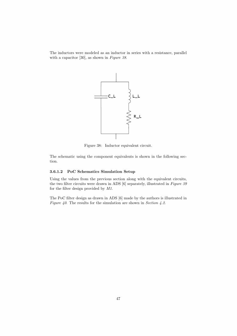
The inductors were modeled as an inductor in series with a resistance, parallelwith a capacitor [30], as shown in Figure 38.
Figure 38: Inductor equivalent circuit.
The schematic using the component equivalents is shown in the following sec-tion.
3.6.1.2 PoC Schematics Simulation Setup
Using the values from the previous section along with the equivalent circuits,the two filter circuits were drawn in ADS [6] separately, illustrated in Figure 39for the filter design provided by M1.
The PoC filter design as drawn in ADS [6] made by the authors is illustrated inFigure 40. The results for the simulation are shown in Section 4.2.
47

Figure 39: Reference PoC filter design with inactive fields in ADS.
48

Figure 40: Authors PoC filter design with inactive fields in ADS.
49

Figure 39 and Figure 40 have inactive fields and are modified in order to easepresentation and comply with Table 8. For a complete simulation setup withvariables and active fields used in the simulation, see Appendix A. The circuitswere simulated using the S-parameter simulation tool in ADS [6], with a startfrequency of 500 Hz, a stop frequency of 4 GHz and 500 MHz step size.
3.6.2 Layout Simulation
In order to comply with the specifications for the high speed front end, men-tioned in Section 3.6.1, the layout of the high speed front end was simulated inADS [6] using the S-parameter electromagnetic simulation.The OBD++ files which were exported for the layout was imported into ADS[6] and controlled so that the alignment was correct. The stackup for the PCBwas included in the ODB++ files and was controlled after import to ADS [6].The layout was divided into two separate simulations, investigating differentareas of interest; the 0 Ω resistor network for choosing the high speed front endinterface (Section 3.6.2.1) and the whole high speed front end (Section 3.6.2.2).Both simulations were performed using the Electromagnetic Model (EM) S-parameter simulation tool in the layout view, and the model was used togetherwith lumped components in the schematics view. In order to use the EM to-gether with lumped components in the schematics, ports needed to be added inthe layout view to connect the components and a symbol had to be created.
3.6.2.1 Specific Section High Speed Front End Layout Simulation
The specific section of the high speed front end that was simulated was the re-sistor network which chooses the coaxial or STQ interface. This was consideredan area of specific interest since it contains 90 degree turns and resistor pads,which is recommended to avoid when designing high speed systems.Therefore, it was concluded that the impact of the design in this specific areawas to be simulated, in order to estimate the impact of these non-ideal features.The area of specific interest is shown as a conceptual image in Figure 41, inorder to show the location of this area on the PCB.
The imported layout was cropped so that only the area of interest was simulated.The impact of the removed electrical objects were considered small, and the re-moved objects reduced the EM simulation time and complexity. Ports wereadded on the pads and the signal traces in order to attach lumped componentsand simulation terminations in the schematics view. Moreover, layer three andfour, i.e. the power plane and secondary side, were removed completely sincethe impact of these layer were considered small enough to approximate to none.This was due to that no specific power was needed for the area of interest, andno signals were routed on layer four underneath the area of specific interest, aswell as the existence of a ground layer on layer two. Layer one contained all therouted high speed signals for this simulation.The ports connecting the Surface Mount Device (SMD) used a ”delta gap” cal-ibration, while all other ports used no calibration. All ports used 50 + 0i Ωreference impedance. The EM was simulated using a 2D-distributed solver forlayer two, a 3D-distributed solver for layer one and the stitching vias was ap-proximated as lumped, using the lumped via solver. The simulation setup was
50

Figure 41: Conceptual image of the PCB showing the area of special interestfor the EM.
a Momentum Microwave (Mom uW) from 1.5 GHz to 3 GHz with 50 steps.This was done for both the serializer and deserializer layout, since some differ-ences existed as shown in the cropped specific layouts in Figure 42 and Figure43.
Figure 42: Simulation layout of the serializer special area of interest, withcomments explaining the placements of the components.
Two new schematics were made, one for the serializer and one for the dese-rializer. The serializer EM was imported twice into the serializer schematics,and the EM was connected to passive components for the coaxial and STQinterface. The two circuits were terminated with S-parameter simulation ter-minations with 50 + 0i Ω for the coaxial interface and 100 + 0i Ω for the STQ
51

Figure 43: Simulation layout of the deserializer special area of interest, withcomments explaining the placements of the components.
interface and was simulated using the S-parameter simulation from 1.5 GHz to3 GHz in 50 steps. The simulations results are presented in Section 4.2.
3.6.2.2 Complete High Speed Front End Layout Simulation
The complete high speed front end layout was simulated in order to compare theresults with the specifications given for the SerDes ICs that were used. In orderto reduce the simulation time for the EM, the components not related to thehigh speed front end was removed, along with the related layout, conceptuallyshown in Figure 44.
Figure 44: Conceptual Image of the PCB showing the area of interest for theEM model.
The EM that was simulated using the imported layout cropped to only contain
52

the ”area of interest”, as shown above. The impact of the removed electricalobject was approximated to none, since distance between the high speed frontend signals and the removed electrical object was considered large.In order to further reduce the EM simulation time, all stitching vias was ap-proximated to a lumped model, which was the majority of the vias in the areaof interest. The two vias used for the STQ interface front end was howeversimulated using a 3D-distributed via solver.
The ground and power planes were approximated to be simulated with a 2D-distributed solver, since the point of interest regarding the planes was the sta-bility. The top- and bottom-layers were simulated using a 3D-solver in orderto get the most accurate solution, since the signals of interest were located inthese layers. Moreover, some power nets was specifically chosen to be modeledas sheets, since no current was flowing in the power planes during simulation,except the planes related to the PoC filter output, which were modeled as 2D-distributed.
The ports which were used to connect S-parameter simulation terminationsin the schematics view were modeled with the no calibration model. The portwhich was used for measuring the output of the PoC filter used no calibration,and the ports which was to be connected to the lumped components were cali-brated using the ”delta gap” calibration model. All remaining ports, which wereused to connect the ground used no port calibration. All ports used 50 + 0i Ωreference impedance. The cropped serializer layout is shown in Figure 45 andthe cropped layout for the deserializer is shown in Figure 46.
Figure 45: Simulation layout for the serializer high speed front end.
Using the above described simulation setting, a Momentum Microwave EM wassimulated from 1.5 GHz to 4 GHz in 50 steps. A new schematic was createdand the model was imported trice, one for the STQ front end interface setupand two for the coaxial front end interface setup with different PoC filters. Thepassive components related to the high speed front end were imported into the
53

Figure 46: Simulation layout for the deserializer high speed front end.
schematics and connected to the model according to the front end schematic foreither STQ or coaxial interface.
The S-parameter simulation controller and terminations were imported and con-nected, and the setup was simulated from 1.5 GHz to 4 GHz using 50 steps. Thiswas done for both the serializer and deserializer layouts.The results of both the serializer and deserializer high speed front end layoutsimulation for both the coaxial and STQ interface are presented in Section 4.2.The EMs for the complete serializer and deserializer high speed front end wereconnected with a cable model in order to test the link quality to compare to thebenchmarks M1 provided. An illustration of the connected simulation setupis shown in Figure 47 where the serializer and deserializer PCBs represent theEM.
54

Figure 47: Illustration of simulation setup for the connected serializer anddeserializer system.
Using the previous S-parameter results from the complete high speed layout sim-ulations would be efficient since the simulation time for each simulation wereextensive. This was done by using the 8-Port S-Parameter(S8P) module andimporting the previous simulated results for the complete high speed layoutschematics.The S8P module was able to accept an eight port S-parameter dataset file,which complied to the previously simulated results, where six of the ports werethe S-parameter simulation results of the input and output of the high speedtraces of different setups described above.
The cables were modelled using the 2-Port S-parameter Equation(S2P Eqn)module which accepts 2-port S-parameters, where S11 and S22 were set to zeroand S12 and S21 were set to the attenuation equation of the cable found in thecable datasheet. In the cases of missing attenuation equations, these were foundby importing the attenuation values into MATLAB [17] and performing ”curvefit”. For the STQ cables, the attenuation was equal for all the cables used inthis thesis, therefore the Leoni Dacar 535 cable represented all STQ cables.
Therefore only the attenuation of the cables were accounted for, and the in-put and output reflection were approximated to zero since no such data could
55

be found for the connectors or cables. The attenuation values of all cables weregiven in dB/m and the setup was tested for 1, 2, 5 and 10 m by multiplying theattenuation by the length of the cable. In order to protect the specifications ofthe high speed link, the curve fit functions will not be disclosed in this report.The cable S2P Eqn modules and SerDes S8P modules were connected and ter-minated with S-parameter simulation terminations according to Figure 47 andan S-parameter simulation controller was imported. The setup was simulatedfrom 1.5 to 4 GHz with 50 steps for each cable and length.In order to compare the simulation results with the link benchmarks providedby M1, the simulated data were exported to a text file and thereafter importedinto MATLAB [17] to be plotted together with the benchmarks. The results ofthe above described simulations are shown in Section 4.2.3.3.
3.7 Software
In order to operate the finished SerDes system, the SerDes ICs had to be prop-erly setup with the desired function. For this, software was written for theon-board MCU to allow for setup and debug of the final system.
3.7.1 Microcontroller Firmware
The firmware needed for the MCU in order to handle initialization and debug-ging of the system was written in the C-language, using the IAR EmbeddedWorkbench IDE and compiler for STM8 microcontrollers [8]. A free ”kick-starter” license of the compiler were used, limiting the maximum code size to 8kB.
The firmware featured a serial port console implementation, using the UARTmodule to print a debug console over the serial port. The serial port was con-nected to the host computer using a USB to UART interface, and operatedusing the terminal software PuTTy [61]. The debug console allows the user toprint the status of the serial link, as well as read and write internal registers inthe SerDes IC’s. The status and the read and write commands involved readingand writing over the I2C bus. A state diagram overview of the debug interfaceis seen in Figure 48.
56

Figure 48: State diagram of the MCU debug interface.
In addition to the general commands presented in Figure 48, a Pseudo-RandomBit Sequence (PRBS) Test and Select Link Speed command was added to thedeserializer debug interface. This to allow for selection between low and highlink speed, as well as testing the link functionality.Both UART and I2C were based on the peripheral drivers provided by STMicro-electronics, and supporting functions such as ”Read” and ”Write” over the I2Cbus were created based on these functions. The UART functions were recoveredfrom an existing example project, and required no further developing in orderto achieve the desired functionality.
During the Prompt Initial Message state shown in Figure 48, both sides ofthe SerDes system are initialized, configuring GPIO and link parameters forproper function of the link. The initialization procedure are further describedin Section 3.7.2.
3.7.2 SerDes Initialization Table
The initialization process of both SerDes ICs followed the same steps with smallvariations in register values. The complete process, involving registers and val-ues could not be disclosed in this report due to the NDA protecting the registermap. A general overview of the process steps is shown in Table 9.
First the deserializer is initialized by the local MCU following the configurationsteps presented in Table 9. After the deserializer is configured, the serializer isinitialized by the deserializer over the serial link, following the same configura-tion procedure as the deserializer.
57

Table 9: Initialization process for the SerDes solution, performed by the on-board MCU
Initialization DescriptionStep
1 Configure link speed
2 Configure I2C pass-through
3 Configure GPIO connection across the link
4 Configure MIPI CSI-2 lane swap as needed
5 Configure MIPI CSI-2 polarity swap as needed
6 Configure video data format
7 Configure internal pipeline routing for output and input port selection
3.8 Layout and Schematics Review
The layout and schematics produced were subject for review in order to vali-date the designs and minimize possible errors and problem areas in the finalizeddesign. The review were performed both by M1 and internally within Autoliv.A full review was performed where the electrical schematics and layout of thetwo designs were evaluated.
The review of the electrical schematics was important in order to verify thatthe desired functionality was met. This as the datasheets and information pro-vided with the SerDes ICs at the design phase were still incomplete, and someelectrical aspects were still subject to possible change. Furthermore, a reviewof the layout was done by both parties, with an extra effort at reviewing thehigh speed traces and power routing, to further minimize possible problem areas.
After the reviews were complete and the review comments had been addressed,the design files were forwarded to the manufacturer for price inquiry and order.
3.9 Ordering and Assembly
In order to test the SerDes systems, the serializer and deserializer sub-systemswere manufactured and assembled, described in this section.
3.9.1 PCB, Cable and Component Ordering
When the design was reviewed and all components availability were checked,the PCB, components and cables were ordered from Autolivs subcontractors.The cable manufacturer was however unable to deliver the desired cables, andtherefore cables were sourced from Autoliv in-house stock.
3.9.2 PCB Assembly
The components were soldered to the PCB using solder paste, hot air oven andsoldering iron in TP4009, Campus Norrkoping, Linkopings University. Dueto time and simplicity reasons, the assembly was done by the authors sincethe number of components were considered low and only the primary side waspopulated.Due to delivery delay, the deserializer PCBs were assembled four weeks after the
58

components were ordered. The deserializer IC was delivered approximately oneweek before the serializer IC, which resulted in a total delay of five weeks betweenordering the components and having assembled the whole SerDes system.
3.10 Testing
The tests conducted on the assembled system are described in this section.
3.10.1 Power-over-Coaxial Filter
The assembled PoC filter designs were tested in TP5004 at Linkopings Univer-sity, Campus Norrkoping. The test of the PoC filter designs performance wasperformed only on the deserializer side, as the serializer side featured the samefilter design. The resulting attenuation of the PoC filters in the actual design,featuring filters on both sides of the link, could therefore be approximated totwice that of the single side results. Both filter designs were tested using thesame test setup, and using the same test parameters. Figure 49 shows the equip-ment setup used for testing.
Figure 49: Complete setup used to test the PoC filter design performance.
The test was performed by populating a PCB with the filter design to be tested,where the coaxial connector were terminated via 50 Ω resistor to ground, insteadof being terminated towards the deserializer IC. The filter was then feed via theFAKRA connector, using the 5 m LEONI Dacar 462 cable. The cable wasconnected to the tracking generator of an Agilent N9320B Spectrum Analyzerusing an adapter card to change from a FAKRA interface to an SMA interface.To probe the filter for measurements, an Agilent N1020A TDR probe was used.Figure 50 shows the probe mounting on the PCB. The filter was tested over thefrequency span 0 to 3 GHz with a 1 MHz bandwidth and -5 dBm amplitude.Each measurements ran in 30 seconds to allow the spectrum analyzer to performseveral sweeps over the frequency span.
59

Figure 50: Probe mounting for test of mounted PoC filters.
For each filter, three measurements were performed, where the measurementprobe was moved slightly each time to verify that the probe had proper con-nection to the testing points. After the filter measurements were performed,both filters were removed, and the attenuation after the FAKRA connector wasmeasured. Due to the 50 Ω impedance of the probe, the last measurementperformed without the filters mounted had an equivalent termination of 25 Ωinstead of the desired 50 Ω termination. The measurement suffered thereforefrom an attenuation bias of -4.77 dB, proportional to the signal reflection seenat the termination. The bias introduced due to said reflection is compensatedfor by adding a 4 dB marginal to the affected measurement results in Section4.3.1. While the compensation with 4 dB is less than the theoretical error, thelower compensation is chosen to allow for imperfections in the actual physicaltest due to factors such as contact resistance and component variations.
3.10.2 EMC Testing
The EMC testing was conducted in the EMC lab TP5004 at Linkopings Uni-versity, Campus Norrkoping, where the goal was to derive the EMC impactthat the cable have in the complete SerDes system. The measurements wereused as an indication on how the cable would compare to each other and to thestandards for radiated emissions in the automotive industry.
While international and national EMC standards exists for both on- and in-board performance, car manufacturers can have internal specifications for thesetests [67].For this thesis, only the CISPR standard was investigated, and only on-boardradiated emissions covered by CISPR 25 was of interest [68].Notable is that the focus was on the cable, since the end product use of theSerDes system would be integrated to the actual product design, which often
60

are enclosed in metal heat shields. The serializer and deserializer PCBs in thisthesis will not be mounted in a car nor sold, and would therefore not need tocomply with these regulations.
However, the EMC measurements of the cables were dependant on the SerDesICs being active, resulting in the SerDes platforms being present during theduration of the test. To reduce the impact of the SerDes platforms in the mea-surements, the SerDes PCBs were placed inside shielding boxes, seen in Figure51.
Figure 51: Shielding box used to house the SerDes PCBs.
The CISPR 25 standard requires an anechoic chamber of a certain size [67],which the anechoic chamber at Linkopings University, Campus Norrkoping doesnot comply with. However, the results would still be valid as a base for discus-sion about the expected EMC performance and comparison of the cables.
Each cable was tested in two different measurement setups, where several mea-surements were performed and the position of the cable was changed. The worstcase measurements was selected in each case. The cables were tested in the ane-choic chamber, using the test setup illustrated in Figure 52.
The anechoic chamber measurements were focused on radiated emissions, andthe system was setup so that the radiated emissions from the cable would bemeasured. Both the deserializer and serializer were placed in said shieldingboxes and a linear power supply was used in order to minimize the radiatedemissions from the power supply. In order to ensure stable operation of thelink, the power supply output voltage rails were checked using multimeters andthe link status was checked using a computer connected to the UART prior to
61

Figure 52: Illustration of test setup for radiated emission measurement.
the measurements being conducted. The computer and UART to USB converterwere not present in the chamber during the measurements.Table 10 show the equipment used in the radiated emission measurements, andTable 11 show the spectrum analyzer settings used in the radiated emissionmeasurements.
Table 10: Instrument declaration used in radiated emission measurements
Manufacturer Model Number Description
Agilent N9302B 3 GHz spectrum analyzer
Powerbox AB 3000 A Dual output linear power supply
N/A N/A Shielding Boxes
The Eaton Corporation 96001 Double ridge guide horn antenna
Belling Lee - anechoic chamber
Table 11: Spectrum analyzer frequency settings used in radiated emission mea-surements
Test No. Resolution Bandwidth Frequency Span Center Frequency
1 100 kHz 100 MHz Low speed mode
2 10 kHz 100 MHz Low speed mode
3 100 kHz Zero Span Low speed mode
4 100 kHz 200 MHz High speed mode
5 10 kHz 200 MHz High speed mode
6 100 kHz Zero Span High speed mode
The input gain of the spectrum analyzer was set to 10 dB in order to lowerthe noise floor, providing a noise floor around -90 dBm with 10 kHz resolutionbandwidth.
3.10.3 Link Quality Measurements
The quality of the link in terms of link margin was measured using a debuggingtoolbox provided by M1, able to read out the link margin at the serializer and
62

deserializer side. The toolbox included debug hardware, connected to the de-serializer via the I2C bus. The debug hardware was connected to a computerrunning the debug GUI that allowed readout of said measurement. Measure-ments were done for all of the cables presented in Table 2.
For all cables and PoC filters, the measurements were performed with the SerDeslink running in both low and full speed mode in order to verify the function overthe complete link speed spectrum. The measurement span of the link margintest where given in signal amplitude, where the forward and reverse channelwere tested within a given amplitude span. In order to disclose the results, themeasurement results were normalized against the full span of the forward andreveres channel measurements. This allows the results to be presented in per-centage of the measured span where the link transmitted data without errors,instead of the actual signal amplitude span. The measurements of link mar-gin was compared to values that was considered ”good enough” by M1. Thesemargins were then used to rank each cables with pass or fail for each of theperformed test. The minimum values for a test to be considered passed wasapproximately 42 percent for the forward channel and 75 percent for the reversechannel, where both values had to be reached for the cable to pass.
The eye diagram measurements method was protected by NDA, and the methodin which the eye diagrams were produced can therefore not be disclosed in thisreport. The eye diagram measurements was conducted for each cable and PoCfilter, where the eye diagram was presented as an image.The comparison between the eye diagram measurement results was done interms of zero-crossing jitter, since the link quality measurements covers the am-plitude and thereby loss, and the resulting eye diagram images having too lowresolution in order to make accurate comparisons of either overshoot or ringing.No absolute values could be disclosed due to the NDA.
3.10.4 Complete System
Due to external factors that resulted in a delay of the design and assembly ofthe demonstration platform, the test of the complete system together with theVP and camera are not disclosed within this report. Instead the results arefocused around verifying the SerDes link function and quality, discussed in Sec-tion 3.10.3.
However, the process of finalizing the demonstration platform, and testing ittogether with the camera and VP was to be continued outside of the time frameof this thesis.
63

64

4 Results
The results of the market survey, simulations and tests described in previoussections are presented in this section.
4.1 Market Survey
The compiled results of the market survey are shown in this section. The com-piled information is divided over a series of tables, presenting both an overviewof found systems, as well as an overview of different key system specifications.
Table 12 shows an overview of the available and upcoming solutions and an es-timation of the design complexity of the system. Furthermore, Table 13 presentsome of the key specifications used when comparing the solutions. However,some specifications are presented in a generalized way, or left undisclosed, dueto active NDAs.
The complexity was estimated and based on IC packages, minimal number ofICs needed and total component count. Where complexity is not listed, there isnot enough available information in order to make an assumption. In the casesof the SerDes solution being under NDA, the part numbers are replaced withthe number of individual ICs involved.
Table 12: Overview of found SerDes solutions, and system cost and complexity
Manufacturer Part Number Complexity Availability
M1 Two ICs (Ser+Des) Low Sampling start17Q2
M2 Single IC (Ser+Des) High -
Texas Instruments (TI) DS90UB953 Medium Sampling start& DS90UB9(54/60) 17Q2-Q3
Silicon Line SL83215 & SL83115 High Available
Lattice Semiconductor LIF-MD6000-6MG81I High Available/ LIA-MD6000-80
The SerDes solution chosen to be implemented within this thesis is the one pro-vided by M1 in both Table 12 and Table 13. The specifications in Table 13 seenbelow are presented as given by the manufacturer, and in case of conflict withthe NDAs, the upper limit specified as within Section 1.3 is given.
65

Table 13: Key specifications of the found SerDes solutions
Specification M1 TI Silicon Lattice M2-Line Semicond-
uctor
Link Bandwidth >3 Gbps 4 Gbps 4 Gbps 1.2 Gbps > 100(Max) per Lane Mbps
Link Interface Coax Coax Optical N/A STP/STP /STP
4-lane MIPI Yes Yes Yes Yes YesCSI-2 Support
Compliant no. Yes No No Data Yes Yesof GPIOs
I2C interface Yes Yes No Data Yes Yes
Need External No No Yes - -Driver
Video No No No No YesCompression
Power TBD 325mW 18/42mW TBD TBDConsumption (per IC)(typ)
Automotive Yes Yes No Yes YesGrade
IC Package QFN QFN QFN BGA BGA
Most solutions were fully compliant with the specifications required within thisthesis regarding e.g. MIPI CSI-2 and bandwidth. However, only the solutionfrom M1 proved feasible in terms of system complexity and time frame. Thesolutions from Lattice and M2 both involved more complex PCB design as bothfeatures at least two Ball Grid Array (BGA) components, while the other solu-tions featured the less complex Quad Flat pack No lead (QFN) package.
While most solutions presented in Table 12 and Table 13 uses the coaxial and/orSTP interface, alternative solutions exist, such as the solution from Silicon-Line.While the Silicon-Line require an external driver for its optical link, the possibleEMC aspects related to the transfer medium is removed. However, the utiliz-ing of optical cable removes the possibility for power transfer using the samemedium as in the case of coaxial and STP cables. This removes some of theflexibility related to the traditional copper transfer medium, as power supply tothe remote side would need to be provided from another source.
The solution from M2 differentiates from other solutions as it utilizes a 100Mbps 802.3bw link over only a STP to transfer the data. This is solved bycompression of the camera data, which impose information loss in the data asthe compression algorithm is lossy. With regards to Sections 1.4, M2 ’s solutioncould not be used.
4.2 Simulation Results
The results of the simulations for the PoC filter and high speed front end layoutare shown in this section.
66
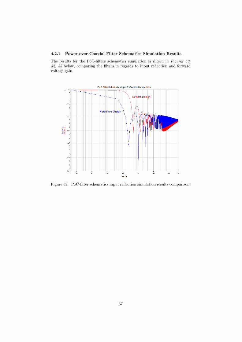
4.2.1 Power-over-Coaxial Filter Schematics Simulation Results
The results for the PoC-filters schematics simulation is shown in Figures 53,54, 55 below, comparing the filters in regards to input reflection and forwardvoltage gain.
Figure 53: PoC-filter schematics input reflection simulation results comparison.
67
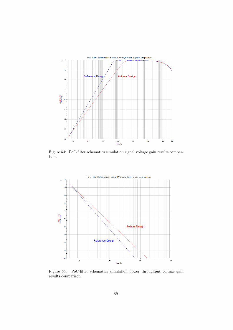
Figure 54: PoC-filter schematics simulation signal voltage gain results compar-ison.
Figure 55: PoC-filter schematics simulation power throughput voltage gainresults comparison.
68
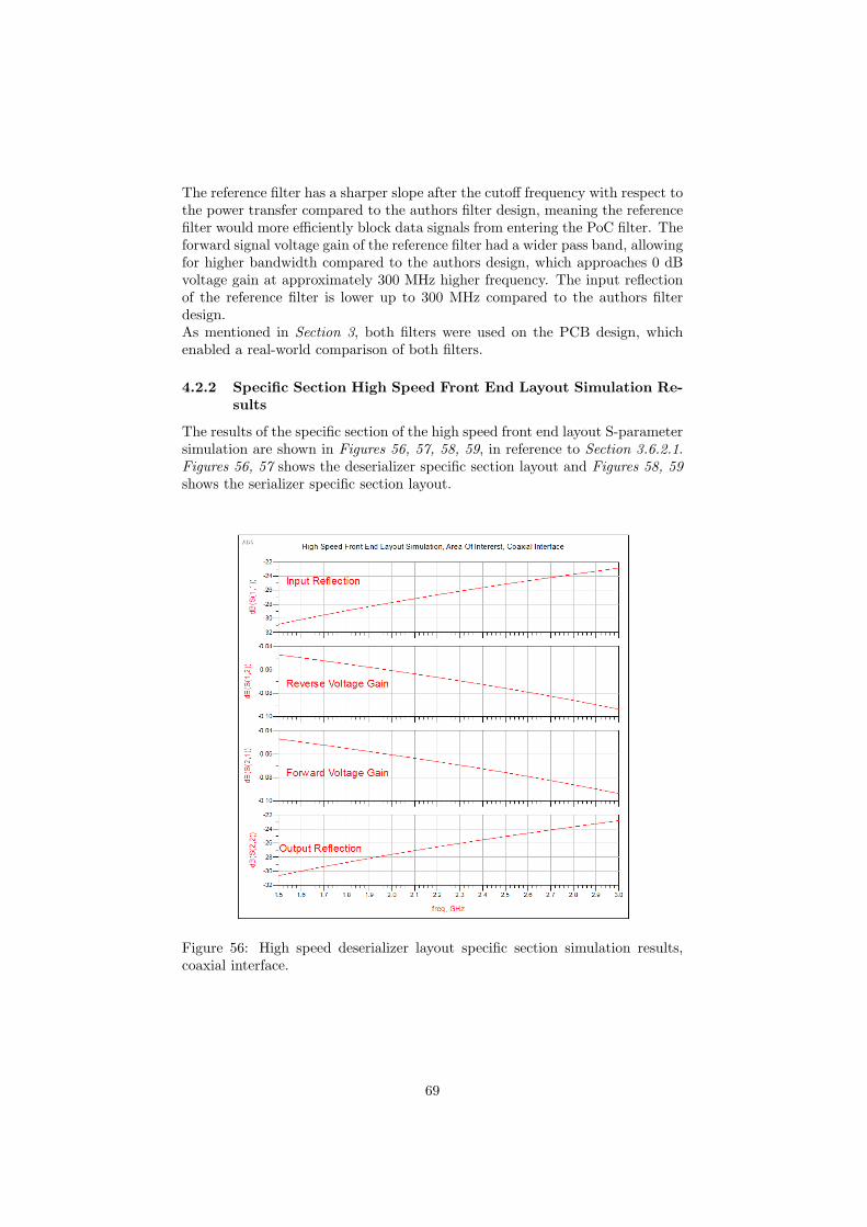
The reference filter has a sharper slope after the cutoff frequency with respect tothe power transfer compared to the authors filter design, meaning the referencefilter would more efficiently block data signals from entering the PoC filter. Theforward signal voltage gain of the reference filter had a wider pass band, allowingfor higher bandwidth compared to the authors design, which approaches 0 dBvoltage gain at approximately 300 MHz higher frequency. The input reflectionof the reference filter is lower up to 300 MHz compared to the authors filterdesign.As mentioned in Section 3, both filters were used on the PCB design, whichenabled a real-world comparison of both filters.
4.2.2 Specific Section High Speed Front End Layout Simulation Re-
sults
The results of the specific section of the high speed front end layout S-parametersimulation are shown in Figures 56, 57, 58, 59, in reference to Section 3.6.2.1.Figures 56, 57 shows the deserializer specific section layout and Figures 58, 59shows the serializer specific section layout.
Figure 56: High speed deserializer layout specific section simulation results,coaxial interface.
69

Figure 57: High speed deserializer layout specific section simulation results,STQ interface.
70

Figure 58: High speed serializer layout specific section simulation results, coax-ial interface.
71

Figure 59: High speed serializer layout specific section simulation results, STQinterface.
72

4.2.3 Complete High Speed Front End Layout Simulation Results
The results for the different configurations of the complete high speed frontend simulations are shown in this section. The deserializer high speed front endlayout results are presented in Section 4.2.3.1 and the serializer high speed frontend layout simulation results are presented in Section 4.2.3.2. The simulationresults of the serializer and deserializer connected with a cable model is shownin Section 4.2.3.3.
4.2.3.1 Complete Deserializer High Speed Front End Simulation Re-
sults
The results for the deserializer high speed front end layout S-parameter simu-lations is shown in Figures 60, 61, 62, where Figure 60 shows the results forthe coaxial interface with the reference PoC filter, Figure 61 shows the resultsfor the coaxial interface with the authors PoC filter and Figure 62 shows theresults for the STQ interface.
Figure 60: High speed deserializer front end full layout simulation results,coaxial interface with reference PoC filter.
73

Figure 61: High speed deserializer front end full layout simulation results,coaxial interface with the authors PoC filter.
74

Figure 62: High speed deserializer front end full layout simulation results, STQinterface.
75

4.2.3.2 Complete Serializer High Speed Front End Simulation Re-
sults
The results for the serializer high speed front end layout S-parameter simulationsis shown in Figures 63, 64, 65, where Figure 63 show the results for the coaxialinterface with the reference PoC filter, Figure 64 show the results for the coaxialinterface with the authors PoC filter design. Figure 65 show the simulationresults for the STQ interface.
Figure 63: High speed deserializer front end full layout simulation results,coaxial interface with reference PoC filter.
76

Figure 64: High speed deserializer front end full layout simulation results,coaxial interface with the authors PoC filter.
77
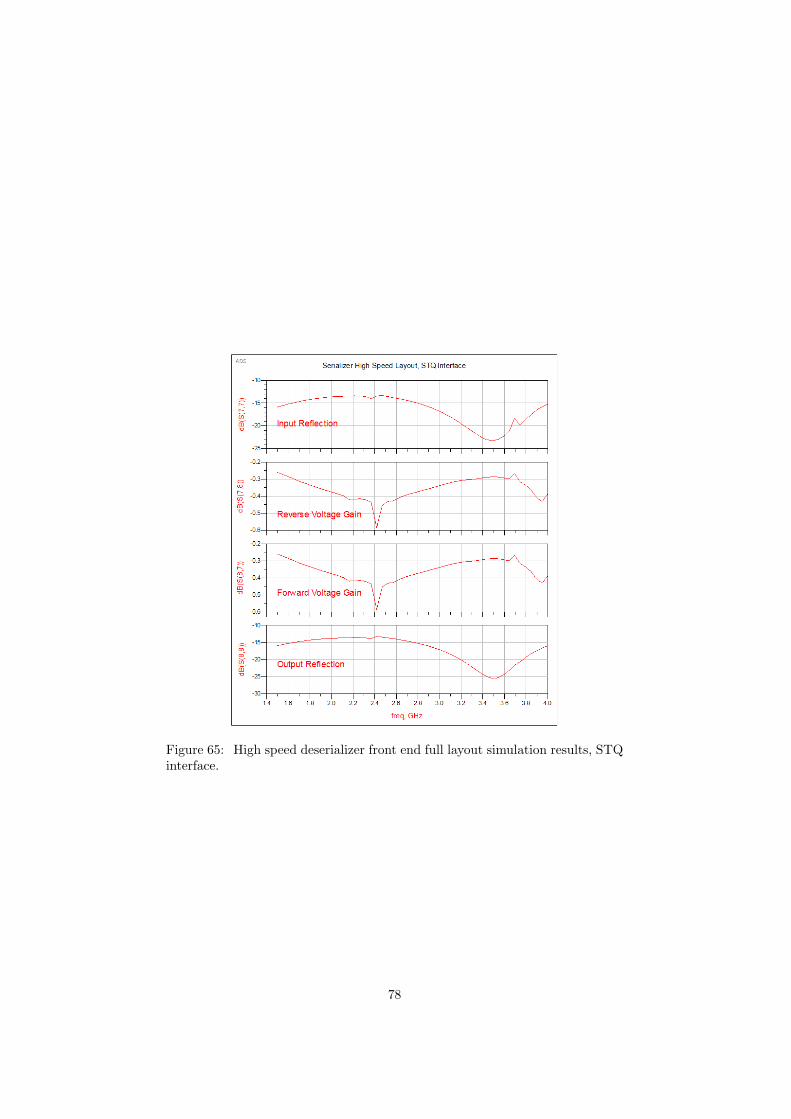
Figure 65: High speed deserializer front end full layout simulation results, STQinterface.
78

4.2.3.3 Serializer and Deserializer High Speed Front End And Bench-
marks Comparison
M1 provided key specifications which needed to be followed for the high speedfront end, consisting of Insertion Loss (IL), Return Loss (RL) and IRR, as de-scribed in Section 3.5.3.
The S-parameter simulation results of the high speed front end and benchmarkcomparison is shown in Appendix B, where the values on the y-axis is not dis-closed due to the NDA. However, the simulation results of the complete systemusing different cable with varying lengths is presented as a comparison with thegiven the specifications. The ”Y ” value on the y-axis found in the simulationresults figures is a placeholder for a value and is the same in each figure in orderto compare the results.
The green area named Specification Passed Area illustrates an area in whichthe results graph must be inside in order to pass the benchmark.According to M1, the link must pass the insertion loss specification and eitherthe return loss or IRR specification to pass the benchmark. A compilationof which cables and filter simulation results which passed the specifications isshown in Table 17.
4.3 Functional Test Result
The test results provided by the functional tests made on the manufacturedSerDes system is presented in this section.
4.3.1 PoC Filter Results
The results for the PoC filter were twofold, while the functionality is prioritized,footprint is a factor which affects the total size, weight and cost of the system.
4.3.1.1 PoC Filter Footprint
The footprint of the two different PoC filters on the PCB design are shown inTable 14.
Table 14: PoC Filter Footprint Measurements
Measurement Reference Filter Authors Filter
Component Footprint [imperial] 0603 + 0603 + 1008 0402 + 0603
Component Footprint sum [mm2] 7.56 1.78
Design Size, serializer [mm2] 20.1 6.3
Design Size, deserializer [mm2] 19.1 4.2
As seen in Table 14, the authors PoC filter footprint was 31% of the referencefilter design footprint on the serializer side and 22% of the reference filter designsize on the deserializer side. Using only the component footprint size codes, theauthors filter footprint is 23% of the reference filter footprint.
79

4.3.1.2 PoC Filter Functionality Measurements
The results of the attenuation measurements of the PoC filters are shown inFigures 66, 67, where Figure 66 shows the measured attenuation before andafter both filter designs when feed via a 5 m LEONI Dacar 462 cable. Figure67 shows the resulting attenuation in the filters.
Figure 66: Attenuation measured after and before both PoC filter designs.
The attenuation of the filters is derived using the measurements seen in Figure66 by deriving the margin of the attenuation before and after both filters.
Figure 67: Relative attenuation for reference and author designed PoC filters.
The measured DC resistance was 1.2 Ω with a deviation of 0.5 Ω.
80
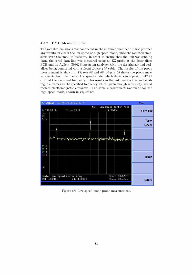
4.3.2 EMC Measurements
The radiated emissions test conducted in the anechoic chamber did not produceany results for either the low speed or high speed mode, since the radiated emis-sions were too small to measure. In order to ensure that the link was sendingdata, the serial data line was measured using an EZ probe at the deserializerPCB and an Agilent N9302B spectrum analyzer with the deserializer and seri-alizer being connected with a Leoni Dacar 462 cable. The results of the probemeasurement is shown in Figures 68 and 69. Figure 68 shows the probe mea-surements front channel at low speed mode, which depicts in a peak of -17.71dBm at the low speed frequency. This results in the link being active and send-ing idle frames at the specified frequency which, given enough sensitivity, wouldradiate electromagnetic emissions. The same measurement was made for thehigh speed mode, shown in Figure 69.
Figure 68: Low speed mode probe measurement.
81

Figure 69: High speed mode probe measurement.
Since the probe introduces a 50 Ω load parallel to the IC load, resulting in a 25Ω termination which introduces reflection into the link. The probe load affectsthe amplitude of the measured signal, which in reality is larger than -17.71 dBm.The added attenuation as a result of the reflection is 4.77 dB, meaning the realamplitude was closer to -12.94 dBm.
In order to test the link without the parallel load, the FAKRA to SMA con-nector used in the PoC filter functionality measurements was used, connectingonly the serializer or deserializer in (line) to the spectrum analyzer. The resultsfor these measurements are shown in Figures 70 and 71, where Figure 70 showsthe back channel measurements from the deserializer and Figure 71 shows thelow speed front channel from the serializer.
82

Figure 70: Reverse channel in line measurements.
Figure 71: Forward channel, low speed mode in line measurement.
83
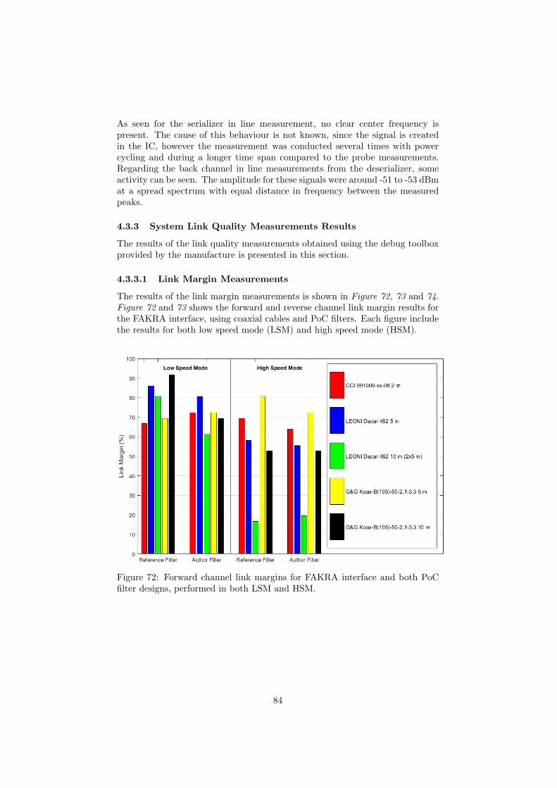
As seen for the serializer in line measurement, no clear center frequency ispresent. The cause of this behaviour is not known, since the signal is createdin the IC, however the measurement was conducted several times with powercycling and during a longer time span compared to the probe measurements.Regarding the back channel in line measurements from the deserializer, someactivity can be seen. The amplitude for these signals were around -51 to -53 dBmat a spread spectrum with equal distance in frequency between the measuredpeaks.
4.3.3 System Link Quality Measurements Results
The results of the link quality measurements obtained using the debug toolboxprovided by the manufacture is presented in this section.
4.3.3.1 Link Margin Measurements
The results of the link margin measurements is shown in Figure 72, 73 and 74.Figure 72 and 73 shows the forward and reverse channel link margin results forthe FAKRA interface, using coaxial cables and PoC filters. Each figure includethe results for both low speed mode (LSM) and high speed mode (HSM).
Figure 72: Forward channel link margins for FAKRA interface and both PoCfilter designs, performed in both LSM and HSM.
84
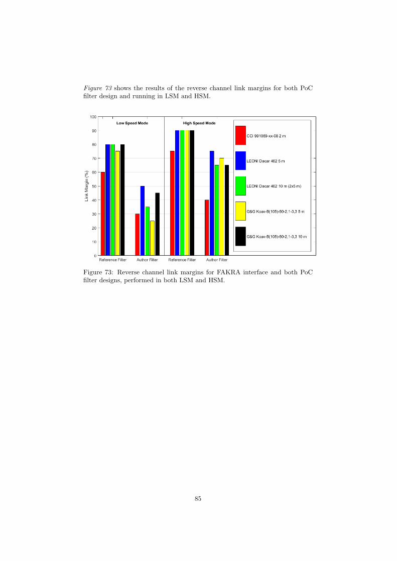
Figure 73 shows the results of the reverse channel link margins for both PoCfilter design and running in LSM and HSM.
Figure 73: Reverse channel link margins for FAKRA interface and both PoCfilter designs, performed in both LSM and HSM.
85

Figure 74 shows the link margin results for the STQ cables, including both theforward and reverse channel link margins in LSM and HSM.
Figure 74: Forward and reverse channel link margins for STQ interface in bothLSM and HSM.
4.3.3.2 LVDS Eye Diagram Measurement Results
The eye diagrams provided a visual representation of the link quality and jitterpresent in the link. The resulting images of the eye diagram measurements willbe presented in this section, as well as a comparison between zero-crossing jitter.The zero-crossing jitter was compared with regards to forward or reverse chan-nel, cable type with the same length, PoC filter and transfer speed.The eye diagram measurements are presented in Figures 75, 76 and 77, whereFigure 75 shows the reverse channel eye diagrams for different 10 m cables andfilters, Figure 76 shows the low speed front channel eye diagram for different10 m cables and filters, and Figure 77 shows the high speed front channel eyediagram for different 10 m cables and filters.
86

Figure 75: 10 m cables reverse channel eye diagram comparison.
Figure 76: 10 m cables low speed forward channel eye diagram comparison.
87

Figure 77: 10 m cables high speed forward channel eye diagram comparison.
The eye diagram measurements for the 5 m Leoni Dacar 538 is shown in FigureC.1 and the 2 m CCI 991069-xx-08 is shown in Figure C.2 in Appendix C. The5 m cables eye diagram comparison is not disclosed in this report, since the 5m cables were of the same type as for 10 m with the exception of the LeoniDacar 538 and the 10 m is considered the worst case scenario and would pro-vide a comparison in itself. The comparative results will therefore be based onthe 10 m cable eye diagram measurements, these results is presented in Table 15.
The compiled eye diagram results for the 10 m cables were compared by measur-ing the width of the zero-crossing in the images. The results are presented witha scale of smallest, widest and middle, where smallest means least zero-crossingjitter. This is due to the comparative element only being the cables, since nospecifications for the zero-crossing jitter was given. The choice of scale is dueto the inability to accurately measure exact time in the images.The compilation results will only be presented where the comparison is measur-able, otherwise it is noted as not measurable (NM).
Table 15: 10 m cable eye diagram zero-crossing jitter measurement compilation
Channel/ Filter Reverse LSM Forward HSM ForwardCable Channel Channel Channel
LEONI Dacar 535-2 N/A Smallest NM Widest
LEONI Dacar 462 Reference Middle NM MiddleFilterAuthors Widest NM MiddleFilter
G&G Koax-B(105) Reference Middle NM Smallest-50-2,1-3,3 Filter
Authors Middle NM MiddleFilter
In the case of the low speed mode forward channel, the zero-crossing was one
88

or no pixels wide in the image, making a comparison unfeasible.
4.4 Compiled Cable Results
The compiled results for the cables shown in Table 2 is presented in this section.Table 16 contains the results of the link function test, running the link margintest in both low and high speed mode for both PoC filter designs.
Table 16: Cables passing or failing the link margin test minimum levels
Cable Length Low Speed Mode High Speed Mode
LEONI Dacar 535-2 10 m Passed Failed
LEONI Dacar 538 5 m Passed Failed
LEONI Dacar 462 5 m Passed (only with Passedreference filter)
10 m Failed Failed
G&G Koax-B(105)-50-2,1-3,3 5 m Passed Passed (only withreference filter) reference filter)
10 m Passed Passedreference filter) reference filter)
CCI 991069-xx-08 2 m Failed Passedreference filter)
In Table 17, the IL, RL and IRR simulation pass or fail results for the completesystem for each cable is compiled and presented. The results are presented aspass or fail, as compared to the acceptable levels specified by M1.
Table 17: Results of simulated system IL, RL and IRR for the different cablescompared to specified acceptable levels
Cable Length Low Speed Mode High Speed Mode
LEONI Dacar 535-2/538 1 m Failed Failed2 m Failed Failed5 m Failed Failed10 m Failed Failed
LEONI Dacar 462 1 m Passed Passed2 m Passed Passed5 m Passed Passed (only with
reference filter)10 m Passed (only with Passed (only with
reference filter) reference filter)
G&G Koax-B(105)-50-2,1-3,3 1 m Passed Passed2 m Passed Passed5 m Passed Passed (only with
reference filter)10 m Failed Failed
CCI 991069-xx-08 1 m Passed Failed2 m Failed Failed5 m Failed Failed10 m Failed Failed
89

90

5 Discussion
This section will discuss the implementation and results obtained in this thesis.
5.1 Market Survey Discussion
By interpreting the result of the market survey presented in Section 4.1, theavailability of SerDes solutions that fulfill all the specifications and limitationsof the system was few. While the available solutions presented within this the-sis is limited, it is worth pointing out that several high-speed SerDes solutionsexist on the market, able to handle a vast amount of signal types such as LVDSand Parallel video among others. However, only a fraction of the system on themarket support the MIPI CSI-2 standard.
Of the solutions presented within this thesis, only the systems delivered fromM1, M3, Texas Instruments and Silicon-Line was able to handle both the re-quired bandwidth and desired input interface. The solution from Lattice Semi-conductor, being a FPGA system, provide extra flexibility in the system itself.However, with the limitation in bandwidth, with a maximum of only 1.2 Gbpsper lane and Input-/Output pin, a total of three twisted pars would be needed inorder to achieve the desired bandwidth, making the cable more complex. Whilebeing limited by the bandwidth, the flexibility of the Lattice Semiconductor so-lution prove to make it a good solution for larger systems, where an additionalSerDes solution that are able to handle arbitrary LVDS signals could be used.
The alternative solution presented by M2, utilizing the 802.3bw Ethernet stan-dard and video compression to provide a video link over a 100 Mbps STP in-terface, further allows for interesting applications. The solution is implementedaround a System-On-a-Chip system, identical on both ends. This makes it suit-able to perform additional task, such as running image algorithms while alsoproviding support for common Ethernet protocols. However, the video com-pression makes it unsuitable for certain ADAS systems as it introduces extraoverhead as the video compression need to be considered in the image algo-rithms, as well as adding an uncertain factor to the video feed due to the lossin information due to the compression algorithm.
The Silicon-Line differentiates itself from the other solutions, were it utilizes anoptical transfer medium instead of the traditional copper based wire medium.While this adds the need for an line driver if it is to be used in the systemproposed within the thesis, the EMC aspects of the cable removed due to theuse of light. However, the need to power the device over the cable require spe-cial cables, combining both the optical fiber and two copper wires for powertransfer. This would most likely introduce not only a high cable cost, but alsomaking the cable less flexible than the alternatives, making it not suitable forbeing used in a wide range of automotive systems.
The two solutions manufactured by M1 and Texas Instruments were both verysimilar in function and performance, both being well suited for the applicationpresented in this thesis. However, the solution from Texas Instruments did notprovide enough GPIO in order to fully comply with the VP and camera system
91

used within this thesis. To address this, additional logic would be needed in thedesign in order to provide GPIO expansion possibilities, further increasing thecomplexity of the design. The solution from M1, being the solution chosen tobe implemented, fulfilled all the needs for the proposed system, while also beingavailable for sampling, making it the best candidate for the implementation atthe time of the thesis.
The fact that the best suited solutions presented within the thesis, manufac-tured by M1, M3 and Texas Instruments, are not yet commercially availablegives an indication on the state of the field, where this type of specialized cir-cuits are to be considered state-of-the-art. This severely impacted the choice ofsolution, as the selected solution had to be available within the time frame ofthe thesis.
A sixth SerDes solution was presented by a manufacturer (from here on ref-ered to as M3 ) at the end of the thesis work, with expected sample deliveryduring 2018. However, since this solution was still in IC prototype stage, nohard specifications were given more than an estimated throughput higher thanall above presented solutions. No data about this solution can however be dis-closed in this report, partly due to that specifications were subject to changeand the performance estimations were protected by a NDA. This solution washowever disclosed in the documentation delivered to Autoliv.
5.2 System Discussion
The results of the simulations, together with the measured results, are discussedin the following subsections.
5.2.1 PoC Filter Discussion
The PoC filter simulations were done in order to ensure that the function of thefilter was sufficient for blocking out the signal frequencies while not affectingthe DC power transfer. The filter performance designed by the authors wascompared to that of the reference filter given by M1. The results of the PoCfilter simulations show that due to a narrower pass band in the forward voltagesignal gain comparison (Figure 54) the authors design would not be as efficientfor data signals under 3 MHz, in comparison with the reference filter which hasthe same efficiency around 800 kHz. The back channel frequency for the appli-cable serial links found in the market survey was however above 3 MHz, makingthe narrower pass band of the authors design functional for the back channel.Regarding the higher frequency front channel, the reference design and the au-thors design converge to similar values for both forward voltage signal gain andinput reflection, making the authors design theoretically ”as good” as the ref-erence filter design.The forward voltage power gain for the PoC filters only needs to be low impedancefor low frequencies, due to the DC, and the negative slope of both filter wereconsidered sufficient enough for blocking the front- and back-channels, e.g. thereference filter reaches -50 dB at 5 kHz and the authors filter reach -50 dB at7.5 kHz.Looking at the simulation results for the PoC filters in comparison with the
92

functionality, the authors filter design would be a quarter of the size of the ref-erence filter, while still providing similar functionality. The measurements thatwas performed on the assembled filter when mounted on the PCB were limitedto the noise floor, as seen in Figure 66, where the attenuation behind both filtersare almost completely equal, except from a small spike in lower frequencies forthe reference filters. Due to the measurements being limited by the noise floor,the actual performance of the filters could not be measured, but the results stillshowed that the performance of both the reference and author design functionwas sufficient for the appointed function. Taking the attenuation due to boththe serializer and deserializer sides in to consideration, the best case signal at-tenuation would be only half of that measured within the thesis. This due tothe complete system including two filters, lowering the over all impedance byapproximately a factor two. Thus the worst case attenuation would be -15 dBat 3 GHz, as seen in Figure 67 where the attenuation is approximately -30 dBat the given frequency. However, the attenuation is assumed to be higher, asthe attenuation as previously stated, was limited by the noise floor and possiblycould be higher than what could be measured at the time.
When comparing the results of the link quality tests, it became clear that theauthors filter designed was insufficient for the task with a link margin belowthe 75 percent mark which was considered a good margin. The reference filterproved to be working for all of the cables and link speed that was tested exceptfor the CCI cable in low speed mode, where the link failed the reverse channelmark. These results shows that great care and consideration have to be taken into account when designing the PoC filters, both in terms of the physical layoutas well as in component selection. The connection of the filter to the signalline introduce an impedance error, and this have to be minimized to lower thereturn loss of the reverse channel. In regards to component selection, the ma-jor difference between the two filter design was the lack of an inductor in theauthors filter design. The purpose of this inductor is mainly blocking out thefrequencies around the reverse channel and is possibly one of the main reasonto the main difference in performance between the two different filter designs.
5.2.2 High Speed Front End Simulation Discussion
The reason for simulating the specific section of the high speed front end con-sisting of the 0 Ω resistor network was due to the structure not being completelycompliant with the routing guidelines since the pads and fan-out would changethe characteristic impedance on the traces. Moreover, there was some differ-ences in the layout of the serializer and deserializer routing, although the resistornetwork schematics were equal. The main difference was the fan-out, where thedeserializer PCB design had no fan-out, causing the impedance to be correctright up to the pad and entering the pad off-center, while the serializer PCB de-sign had regular fan-out, entering the pad in the center. The simulation resultsof the specific section of the high speed front end layout shows no difference sig-nificant enough to make any conclusions regarding the impact these differencesbetween the deserializer and serializer results, see Figures 56, 57 versus Figures58, 59 .
The complete high speed front end deserializer layout simulation results show
93

a forward and reverse voltage gain around -0.5 dB for the coaxial interface and-0.3 dB for the STQ interface at 1.5 GHz, decreasing to -1 dB to -1.7 dB de-pending on the interface and PoC filter, see Figures 60, 61, 62.The dip in voltage gain at 2.48 GHz shown in the STQ interface is most likelydue to non-idealities in the PCB design, however it resides in a frequency rangewhich is not used by the link.These values are above the channel target requirements given by M1 for thefront channel frequency, which supports the functionality of the design. Specificvalues for the channel target requirements can not be disclosed due to a NDA.
The complete high speed front end serializer layout simulation results showa forward voltage gain of around -0.5 dB at 1.5 GHz for the coaxial interfacewith both filters, and -0.25 dB for the STQ interface at 1.5 GHz. The coaxialinterface with both filters have a forward voltage gain around -4 dB at 4 GHz,which is a higher attenuation compared to the deserializer, but still in consid-erable range for the specifications. The STQ interface have a similar behaviourto the deserializer side, with a dip in the forward and reverse voltage gain at2.42 GHz, and as for the deserializer it resides in a frequency range not used bythe link.
The complete high speed front end simulation, i.e. in reference to Figure 47,was done using the simulation results of the high speed serializer and deseri-alizer front end layout simulations.The connector and cable was approximatedto have no input or output reflection since only data regarding the attenuationwas available. The reason for simulating this was in order to compare the simu-lations to the specifications given by M1. It would also reveal simulation resultsregarding the best suited PoC filter and cable as well as which cables wouldperform in a real world application.However, since limited attenuation data and no reflection data were given forthe cables for the frequencies used in the simulations, the given data neededto be curve fitted. Therefore it was approximated that the attenuation of thecables would follow the fitted curves. This is not necessarily the case due tothe parasitic effects such as the capacitive coupling between the shield and theconductors. However most coaxial cables had given attenuation values acrossa large frequency span, making the curve fit an reasonable approximation ofthe cable attenuation model. The curve fit models for the CCI and STQ cablesthat did not provide specified attenuation above 1 and 1.5 GHz respectively, andcould therefore contain errors at frequencies far beyond the given specification.
The results of the complete high speed front end simulation with the serial-izer and deserializer connected with a cable model correlated with the providedspecifications and behaviour that M1 stated in the link specifications documen-tation.The results for the complete high speed front end connecting the serializer, de-serializer and cable in regards to Table 17 show that the STQ cable should notbe able to comply with the link specs, however the functional testing revealsthat the link works with said cable, concluding that the attenuation simulationfunction might introduce a higher attenuation than a real cable would. Thesame case regards the CCI 991069-xx08 cable, where the 2 m cable works withthe tested system. However, the CCI cable is only rated to 1 GHz which is
94
lower than the frequencies considered in this thesis, as well as the cable beingtheoretically least suited for these frequencies (see Table 4).Over all the simulations were considered useful in the evaluation of the design,and using the ODB++ file format to export the layout facilitated the use ofADS for the simulations, which the authors had previous experience with. Thecomplete layout EM simulations were time consuming, however when the EMwas simulated the remaining simulations was quickly executed.
5.2.3 Cable Discussion
The selection of cables was limited due to availability at the Autoliv site inLinkoping. This resulted in a limited amount of available cables, where only afew different cables in each category (coaxial and STQ) were available. In thecase of coaxial cables, three different brands with different specifications wasavailable and tested, while in the case of the STQ cables, the brand and modelof cables shared similar specification due to the models only differentiating by afamily-generation change. While there would be preferable to perform the teston different brand/models of the STQ cable, the fact that most cables availablebeing from the same brand and cable family shows on its strong position withinthe automotive industry and together with the HSD connector interface. It isworth noting that when investigating possible providers for HSD cable assem-blies, the cable selection was defaulted to the LEONI Dacar 535 cable in all ofthe cases.
Looking at the specification for the coaxial cables tested, presented in Table4, the cable from G&G was expected to be the cable yielding the best resultin both function and from an EMC perspective. This due to the lower signalattenuation, allowing for longer cables as well as the improved shield coverageand lower conductor resistance. While the cable length in many automotiveapplications regarding regular cars would not require cable length above a fewmeters, the improved attenuation per meter could also allow for cheaper/othersolutions. An example would be the PoC-filter, which could allow for a lowerimpedance across the blocked frequency range, thus increasing the attenuationseen due to the filters. However, the improved specifications of the G&G ca-ble versus the LEONI Dacar and CCI cables comes with the cost of increasedweight, where the diameter of the G&G cable is around 15 percent larger thanthat of the Dacar cable, and 25 percent larger than the CCI. Thus the G&Gcable have an increased weight, and require more space than the the other cabels.
The results of the performance of each cable when running the link marginstests, presented in Section 4.3.3.1 and 4.4 showed that nearly all cables thatwere tested could be considered for an actual implementation. While none ofthe STQ cables passed the link margin test in high speed mode, most of thecoaxial cables tested were able to pass all the tests. Among the coaxial cablestested, the 10 m Dacar 462 and 2 m CCI cable were the only two cables thatdid not pass all tests. However, as the 10 m Dacar 462 cable consisted of twolinked 5 m cables, the result can be expected to suffer from the added inlineconnection on the cable. Thus it can be expected that an actual 10 m Dacar462 cable should be able to fulfill the specifications for the link margin. Lookingat Figure 72 and 73, it can be seen that the reason for the CCI cable failing
95

the link margin test when running in low speed mode was due to the reversechannel link margin being below 75 percent. However, the CCI cable passed thetest when the link was running in high speed mode, when the forward channelwas moved further away from the reverse channel.
The reverse channel link margin is greatly depending on the presence of thePoC filter, as can be seen when looking at Figure 74 where no filter was needed,and the link margin is close to perfect across all speed modes. The impactof the PoC filter is further noticed in the link margin results, where only onecoaxial cable passed a link margins test when the authors filter design was used.The difference in the reverse channel link margins in Figure 73 when comparingthe reference filters is large, where only the 5 m Dacar 462 cable reached themark of 75 percent when the link was running high speed mode. This is a clearindication on the impact of the PoC filter design in the system, where only thereference design was good enough for the link to be considered ”good”.Considering the performance of the cables, all of the coaxial cables tested couldbe used in actual applications, where the main factor when selecting the cabletype is the required length and operation environment. With common lengtharound a few meters, most of the cable proved sufficient for a functional SerDeslink. Among the cables, only the STQ cables can be considered unsuited for thelink. However, the STQ cables tested in this thesis is not specified to handlethe complete frequency range required to fully utilize the SerDes link. Usinganother STQ cable, such as the LEONI Dacar 636 cable, specified for twice thefrequency range of that of the Dacar 535-2/538 cables, could prove working forthe complete speed range of the SerDes link. However, even if the STQ cablealternative would be sufficient for the considered task, the increase in cable di-ameter compared to the thickest coaxial cable is at least 30 percent comparedto the G&G cable. The increase in size, as well as weight, makes it harder tointegrate in to products with weight and space restrictions.
Regarding the inability to measure radiated emissions in the anechoic chamber,the radiations are assumed to be too small to measure. Assuming a shieldingeffectiveness of 40 dB (i.e. data for the STQ cables), and a signal energy of -10dBm (the signal measured by the probe was around -17 dBm, assumed to bearound -13 dBm due to the reflection added due to the probe). The strength ofthe radiated energy from the cable, assuming all incoming energy is radiated,would be around -50 dBm (i.e. incoming signal strength minus the shield atten-uation). The radiated emission level of -50 dBm is valid under the assumptionthat all of the signal was radiated and the cable (after the shield) was approx-imated to an antenna with 100% efficiency, which was not a feasible real lifescenario. Since the link was active, and working, during the tests, meaning themajority of the signal propagated between the serializer and deserializer IC.Moreover, there is attenuation of the radiated emission between the cable andantenna and in the antenna and the cable. Using these arguments along withthe measured link power, it was concluded that any radiated emissions wouldbe too small to measure with the equipment available.
96

5.2.4 Noticeable Observations
While the results of the link margin mostly suffered in performance in the re-verse channel, manufacturing variations were observed during the process oftesting that could further affect the link margin for better or worse. Amongother things, a problem at the start of the testing was bad solder joints betweenthe SerDes ICs thermal pad and the thermal pads on the PCB. This affectedthe link margin to the worse, severely decreasing the link margin for each cableand interface. Addressing the problem resulted in an 30-40 percent increase inlink margin.
It is also worth noting that the FAKRA and HSD interfaces used together withthe cables are designed for a limited amount of mating cycles, with the purposeof being connected and disconnected only a few times. Thus the cables used inthe test, being connected and disconnected several times could suffer from weardown in the connections, further affecting the results.
97

98

6 Conclusion
The result of the market survey showed five IC solutions conforming with theinterfaces and throughput stated within this thesis. Of the found solutions, twowere commercially available at the time of the thesis, where the remaining so-lutions were either in early development or engineering sampling phase. Of thefive found solutions, only three systems remain feasible in terms of a completesystem due to the high complexity of some candidates. While all systems con-formed with the specifications for the data throughput, the systems from M2and Lattice Semiconductor impose a more complex design due to the encapsu-lation. These systems impose a higher complexity in terms of as well software,being SoC and FPGA systems in comparison to the other solutions presented,being application specific and thereby less time consuming to configure.
While the higher complexity in software allows for more customized systems,the increased flexibility is not a needed component in the proposed system.While the solution from Silicon-Line provide an interesting alternative to theother solutions using a optical medium, the IC was lacking automotive classifica-tion, which made it unsuited for the proposed system. The remaining solutions,manufactured by M1, Texas Instruments and M3 were better suited for theproposed application, being application oriented, low weight and easy to imple-ment. However, these systems were in either early or late development phase,showing that the market segment for the type of specific SerDes solutions thatwas young at the time of this thesis. The market segment showed a rapid growthwith new products together with an increased demand for similar systems, as aresult of the growing research and adaption of ADAS and autonomous drivingsystems that is currently taking place in the automotive industry. The latencyand power consumption could not be compared due to the majority of the so-lutions being in the development phase.
The tests of the link quality of the designed system using different cables showedthat the PoC filter proposed by the authors as an alternative to the referencefilter was not ideally designed for the intended application. The link margin ofthe reverse channel suffered greater losses compared to the link margin observedin the forward channel.The test of the link quality showed satisfactory performance for most of thecoaxial cables when using the reference PoC filter design. Furthermore, nonoticeable radiated EMC could be measured, with the conclusion that the sen-sitivity of the test equipment was insufficient to measure the signals. Thus theselection of a cable for an actual system is more likely to be dependant on theability to shield against incoming EMI, rather than the radiated emissions dueto the SerDes link. The tests of STQ cables showed that the performance im-pact when moving from low speed mode to high speed mode was noticeable,and both cables could not fulfill the link margins to be considered a good link.However, using a STQ cable such as the LEONI Dacar 636 could theoreticallyimprove the result due to the improved frequency characteristics.
99

100

References
[1] Ratings Explained; Lane Support, EuroNCAP, Accessed 2017-01-31; http://www.euroncap.com/en/vehicle-safety/the-ratings-
explained/safety-assist/lane-support/
[2] S.Morris & T.Wilson, Trends, Challenges and Opportunities in Vision-Based Automotive Safety and Autonomous Driving Systems, CogniVuevia Embedded Vision Alliance, Presentation, Accessed 2017-01-20;http://www.slideshare.net/embeddedvision/trends-challenges-
and-opportunities-in-visionbased-automotive-safety-and-
autonomous-driving-systems-a-presentation-from-cognivue
[3] S. Dabral, S. Kamath & V. Appria, ”Trends in Camera based AutomotiveDriver Assistance Systems (ADAS),” Circuits and Systems (MWSCAS);10.1109/MWSCAS.2014.6908613
[4] 2020 ROADMAP, EUROPEAN NEW CAR ASSESSMENT PRO-GRAMME, EuroNCAP, March 2015, Accessed 2017-01-25; http:
//euroncap.blob.core.windows.net/media/16472/euro-ncap-2020-
roadmap-rev1-march-2015.pdf
[5] SOFTWARE Xpedition Enterprise, Mentor Graphics Corporation 1985-2015;https://www.mentor.com/pcb/
[6] SOFTWARE Advanced Design Systems 2016, Keysight Technologies 2000-2017;http://www.keysight.com/en/pc-1297113/advanced-design-system-
ads?cc=SE&lc=eng
[7] SOFTWARE Saturn PCB toolkit V7.02 (free software), Saturn PCB Design,Inc., Accessed 2017-03-23; https://www.saturnpcb.com/pcb_toolkit.
htm
[8] SOFTWARE IAR Embedded Workbench, IAR Systems, Accessed 2017-04-03;https://www.iar.com/iar-embedded-workbench/
[9] Camera serial Interface, CSI-2 and CSI-3 ,MIPI Alliance, Inc. 2015-03-04, Accessed 2017-01-31; http://mipi.org/sites/default/files/
tutorials/Camera\%20Serial\%20Interface_CSI2_CSI3_Overview.pdf
[10] P. Lefkin & R. Wietfeldt, Understanding MIPI Alliance Inter-face Specifications, Electronic Design, 2014-04-01, Accessed 2017-01-30; http://electronicdesign.com/communications/understanding-mipi-alliance-interface-specifications
[11] Camera Interface Specifications, MIPI Alliance, Inc., Accessed 2017-01-30;http://mipi.org/specifications/camera-interface
[12] MIPI D-PHY Protocol Fundamentals, Agilent Technologies, Inc., Accessed2017-01-31; http://rfmw.em.keysight.com/mod/pdf/axie_u4421a_
mipi_d-phy_protocol_fundamentals_detailed_presentation.pdf
[13] PHY Overview, MIPI Alliance, Inc., 2015, Accessed 2017-01-31;http://mipi.org/sites/default/files/tutorials/M-PHY_C-PHY_D-
PHY_Overview.pdf
101

[14] Physical Layer Specifications, MIPI Alliance, Inc., Accessed 2017-01-30;http://mipi.org/specifications/physical-layer
[15] Understanding and Performing MIPI® D-PHY Physical Layer, CSI andDSI Protocol Layer Testing, Tektronix, Inc., 2010, Accessed 2017-01-31;http://www.tek.com/dl/55W_28277_0_MR_Letter.pdf
[16] Mark Sauerwald, FPD-Link III – doing more with less, Texas InstrumentsInc., Q3 2014, Accessed 2017-02-13; http://www.ti.com/lit/an/slyt581/slyt581.pdf
[17] SOFTWARE MATLAB R2014b, The MathWorks, Inc; https://se.
mathworks.com/products/new_products/release2014b.html
[18] Automotive Infotainment Guide, Texas Instruments Inc., 2016, Accessed2017-02-13; http://www.ti.com/lit/sl/ssay002d/ssay002d.pdf
[19] LVDS Serializer-Deserializer Performance over Twisted Pair Cable, MaximIntegrated Products, Inc. Application Note 2023, Accessed 2017-01-31;https://www.maximintegrated.com/en/app-notes/index.mvp/id/2023
[20] Peffers, Michael,Get Connected: SerDes demystified, Texas InstrumentsInc., May 8, 2014, Accessed 2017-02-08; http://e2e.ti.com/blogs_/b/
analogwire/archive/2014/05/08/get-connected-serdes-demystified
[21] Technical Overview, Serial ATA International Organization, Accessed 2017-02-08; http://www.sata-io.org/technical-overview
[22] Serial ATA (SATA) developer page, Intel Corporation, Accessed2017-02-08; http://www.intel.com/content/www/us/en/io/serial-
ata/serial-ata-developer.html
[23] Patel, Atul,The basics of SerDes (serializers/deserializers) for inter-facing, Planet Analog, 2010-09-16, Accessed 2017-02-08; http://www.
planetanalog.com/document.asp?doc_id=528099
[24] LVDS Owner’s Manual Design Guide, 4th Edition, Texas Instruments Inc.,2012, earlier published by National Instruments Corporation, January 2008,Accessed 2017-01-24; http://www.ti.com/lit/ml/snla187/snla187.pdf
[25] Goldie, John, LVDS, CML, ECL-differential interfaces with odd volt-ages, EETimes, 2003-01-21, Accessed 2017-02-08; http://www.eetimes.
com/document.asp?doc_id=1225744
[26] LVDS Application and Data Handbook, Texas Instruments Inc., November2002, TI Litterature number SLLD009, Accessed 2017-02-08; http://www.ti.com/lit/ug/slld009/slld009.pdf
[27] Stephen Kempainen, Low-Voltage Differential Signaling (LVDS) - Applica-tion Note 1382-6, National Semiconductor for Agilent, now Keysight, May10 2002, publ. nr: 5988-4797EN, Accessed 2017-02-15; http://literature.cdn.keysight.com/litweb/pdf/5988-4797EN.pdf
102

[28] APPLICATION NOTE 3570 LVDS Multimedia Interface Has Bright Fu-ture in Automotive Systems, Maxim Integrated Products, Inc., 2005-08-10, Accessed 2017-02-16; https://www.maximintegrated.com/en/app-notes/index.mvp/id/3570
[29] ELECTRICAL CHARACTERISTICS OF LOW VOLTAGE DIFFER-ENTIAL SIGNALING (LVDS) INTERFACE CIRCUITS, PN-4584rev 1.2, TIA Subcommittee TR-30.2, May 2000, Accessed 2017-02-16; http://ftp.tiaonline.org/TR-30/TR-30.2/Public/2000\
%20Contributions/20005017.pdf
[30] Clayton R. Paul, Introduction to Electromagnetic Compatibility, SecondEdition, Wiley & Sons, Inc., 2008
[31] Andy Kuo, Roberto Rosales, Touraj Farahmand, Sassan Tabatabaei, andAndre Ivanov, Crosstalk Bounded Uncorrelated Jitter (BUJ) for High-SpeedInterconnects, IEEE TRANSACTIONS ON INSTRUMENTATION ANDMEASUREMENT, VOL. 54, NO. 5, OCTOBER 2005, Accessed 2017-02-17; http://www.ece.ubc.ca/~soc/soc/publications/KUO.pdf
[32] Michael Schnecker, Jitter Measurements in Serial Data Signals, LeCroyCorporation, Accessed 2017-02-17; http://cdn.teledynelecroy.com/
files/whitepapers/wp_jittermeasurement_in_serialdatasignals.
[33] Interface Circuits for TIA/EIA-644 (LVDS) Design Notes, Texas Instru-ments, Inc., September 2002, Accessed 2017-02-16; http://www.ti.com/
lit/an/slla038b/slla038b.pdf
[34] DS90C031, DS90C032 LVDS Signal Quality: Jitter Measurements UsingEye Patterns Test Report 1, Texas Instruments Inc., previosly released byNational Semiconductor, October 1994, Acessed 2017-05-11, http://www.ti.com/lit/an/snla166/snla166.pdf
[35] SMSC Design Guide for Power Over Ethernet Applications, SMSC Inc.,2009-09-19, Accessed 2017-02-13; http://ww1.microchip.com/downloads/en/AppNotes/en562768.pdf
[36] Sending Power Over Coax in DS90UB913A Designs Texas InstrumentsInc., june 2014, application note SNLA224, Accessed 2017-02-13; http://www.ti.com/lit/an/snla224/snla224.pdf
[37] Kimberly Versaw, ”Types of Cable Shielding,” AlphaWire, December2015, Accessed 2017-10-5; http://www.alphawire.com/en/Company/Blog/2015/December/Types\%20of\%20Cable\%20Shielding
[38] Understanding Shielded Cable, AlphaWire, 2009, Accessed 2017-5-10; http://www.mouser.com/pdfdocs/alphawire-Understanding-
Shielded-Cable.pdf
[39] Michel Mardiguian, ”Shielded cable: Their Role in Reducing EMISusceptibility and Emissions,” Electronic.nu, Accessed 2017-10-5;https://www.electronic.nu/2016/05/30/shielded-cables-their-
role-in-reducing-emi-susceptibilty-and-emissions/
103

[40] IEEE Std. 1143-2012, textitIEEE Guide on Shielding Practice for Low Volt-age Cables, IEEE, 2012
[41] A Pratical Guide To Cable Selection, Texas Instruments Inc., 2011, earlierpublished by National Semiconductor, October 1993, Accessed 2017-05-10;http://www.ti.com/lit/an/snla164/snla164.pdf
[42] Preventing and Attacking Measurment Noise Problems, Campbell Sci-entific, Inc., 2001, Accessed 2017-05-10; https://s.campbellsci.com/
documents/sp/technical-papers/mnoise.pdf
[43] Jullien, Besnier, Dunand and Junqua, Advanced Modeling of Crosstalk Be-tween an Unshielded Twisted Pair Cable and an Unshielded Wire Above aGround Plane., IEEE Transactions on Electromagnetic Compatibility, vol-ume 55 , NO.1 February 2013 S. Dabral, S. Kamath & V. Appria, ”Trendsin Camera based Automotive Driver Assistance Systems (ADAS),” Circuitsand Systems (MWSCAS); 10.1109/MWSCAS.2014.6908613
[44] A. Knobloch, H. Garbe, J.P Karst, ”Shielded or unshielded twisted-pair forhigh speed data transmission?”,Electromagnetic Compatibility, 1998. 1998IEEE International Symposium on, 1998; 10.1109/ISEMC.1998.750069
[45] John Siau, The Importance of Starquad Microphone Cable, Bench-mark Media, February 12, 2012, Accessed 2017-02-16; https:
//benchmarkmedia.com/blogs/application_notes/116637511-the-
importance-of-star-quad-microphone-cable
[46] Steve Lampen, How Starquad Works, Belden Inc., August 2, 2012, Accessed2017-02-16; http://www.belden.com/blog/broadcastav/How-Starquad-
Works.cfm
[47] Technical Reference, RosenbergerHSD, Accessed 2017-05-10; http:
//www.rosenberger.com/0_documents/de/catalogs/ba_automotive/
AUTO_HSD_TechnicalReferences.pdf
[48] Ian Poole, ”Coaxial Feeder / RF Coax Cable Tutorial”, radio-electronics.com, accessed 2017-02-17; http://www.radio-electronics.
com/info/antennas/coax/rf-coaxial-feeder-cable.php
[49] The Introduction of Coaxial Cables, Caledonian Cables Limited Cor-poration, Accessed 2017-02-17; http://www.caledonian-cables.co.uk/
Coaxia_Cable/Introduction.html
[50] Martin J. Van Der Burgt, Coaxial Cables and Applications, Belden Elec-tronics Division, 2003, Accessed 2017-02-16; http://www.belden.com/
pdfs/Techpprs/CoaxialCablesandApplications.pdf
[51] Ian Poole, ”Coaxial Feeder / RF Coax Cable Impedance”, radio-electronics.com, Accessed 2017-02-17; http://www.radio-electronics.
com/info/antennas/coax/rf-coaxial-cable-impedance.php
[52] Introduction to coaxial cacbles, R.F. elettronica di Rota Franco, Accessed2017-02-17; http://www.rf-microwave.com/uploads/cables/coaxial_
cables_en.pdf
104

[53] ISO 20860-1:2008, Road vehicles — 50 ohms impedance radio frequencyconnection system interface — Part 1: Dimensions and electrical require-ments,International Organization for Standardization, 2008, Accessed 2017-17-03; https://www.iso.org/obp/ui/#iso:std:iso:20860:-1:ed-1:v1:en
[54] Image of FAKRA color and mechanical coding, Accessed 2017-28-03; http://www.whnet.com/4x4/radio/FAKRA.jpg
[55] Product Catalogue, Automotive Connectors, FAKRA/USCAR series R114-R197, Radiall, Accessed 2017-17-03; http://radio.passus.pl/files/
Fakra.pdf
[56] Application Note 4085, Advantages of AC-Coupling in SerDes Applica-tions, Maxim Integrated Products, Inc., Mar 04, 2008, Accessed 2017-29-03;https://www.maximintegrated.com/en/app-notes/index.mvp/id/4085
[57] High-Speed Interface Layout Guidelines,Texas Instruments Application re-port, aug 2014, revised sep 2016, Accessed 2017-03-22, URL: http://www.ti.com/lit/an/spraar7f/spraar7f.pdf
[58] High Speed Layout Design Guidelines, NXP (prev. Freescale Semiconduc-tor), document number AN2536, Rev. 2, 04/2006, Accessed 2017-03-27,URL: http://www.nxp.com/assets/documents/data/en/application-
notes/AN2536.pdf
[59] High-Speed Layout Guidelines, Texas Instruments Application Report, doc-ument number SCAA082, nov 2006, Accessed 2017-03-27; http://www.ti.com/lit/an/scaa082/scaa082.pdf
[60] Technical Support, Chip Beads, TDK Corporation, Accessed 2017-03-28;https://product.tdk.com/info/en/technicalsupport/tvcl/general/
beads.html
[61] SOFTWARE PuTTy (open source software), Accessed 2017-04-03; http://www.putty.org/
[62] LEONI, LEONI Dacar 535-2 Technical Datasheet, version 1.4, August 08,2014
[63] LEONI, LEONI Dacar 538 Technical Datasheet, version 2.0, June 06, 2009
[64] LEONI, LEONI Dacar 462 Technical Datasheet, version 2.10, June 20, 2015
[65] Gebauer & Griller, Gebauer & Griller Koax-B(105)-50-2,1-3,3 TechnicalDatasheet, December 7, 2016
[66] Coleman Cable Inc, Coleman Cable Inc 991069-xx-08 Product Datasheet,August 21, 2006
[67] Rodrigues V., Automotive Component EMC Testing: CISPR 25, ISO11452-2 and Equivalent Standards, ETS-Lindgren, Accessed 2017-05-04;http://www.ets-lindgren.com/pdf/AutomotiveComponentEMCTesting.
105

[68] Standard CISPR 25:2006 Vehicles, boats and internal combustion engines -Radio disturbance characteristics - Limits and methods of measurement forthe protection of on-board receivers IEC
106

Appendices
A PoC Filter Design Setup in ADS
Figure A.1: Reference PoC filter design, S-parameter setup without inactivefields in ADS.
A1

Figure A.2: Authors PoC filter design, S-parameter setup without inactive fieldsin ADS.
A2

B Connected high speed front end layout and benchmarkcomparison simulation result figures
Figures B.1, B.2, B.3, B.4 show the insertion loss comparison results for thecoaxial cables, Figures B.5, B.6, B.7, B.8 show the return loss comparisonresults for the coaxial cables and Figures B.9, B.10, B.11, B.12 show the IRRresults for the coaxial cables. Figure B.13 show the insertion loss, return lossand IRR results for the Leoni Dacar 535 STQ cable.
Figure B.1: Connected SerDes high speed front end insertion loss simulationresults, 1 m coaxial cables.
Figure B.2: Connected SerDes high speed front end insertion loss simulationresults, 2 m coaxial cables.
B1

Figure B.3: Connected SerDes high speed front end insertion loss simulationresults, 5 m coaxial cables.
Figure B.4: Connected SerDes high speed front end insertion loss simulationresults, 10 m coaxial cables.
B2

Figure B.5: Connected SerDes high speed front end return loss simulationresults, 1 m coaxial cables.
Figure B.6: Connected SerDes high speed front end return loss simulationresults, 2 m coaxial cables.
B3

Figure B.7: Connected SerDes high speed front end return loss simulationresults, 5 m coaxial cables.
Figure B.8: Connected SerDes high speed front end return loss simulationresults, 10 m coaxial cables.
B4

Figure B.9: Connected SerDes high speed front end IRR simulation results, 1m coaxial cables.
Figure B.10: Connected SerDes high speed front end IRR simulation results, 2m coaxial cables.
B5

Figure B.11: Connected SerDes high speed front end IRR simulation results, 5m coaxial cables.
Figure B.12: Connected SerDes high speed front end IRR simulation results,10 m coaxial cables.
B6

Figure B.13: Connected SerDes high speed front end insertion loss, return lossand IRR simulation results, Leoni Dacar 535 STQ cable.
B7

C Eye Diagram Measurement Results For The Leoni Dacar538 and CCI 991069-xx-08 Cable
Figure C.1: 5 m Leoni Dacar 538 eye diagram.
Figure C.2: 2 m CCI 991069-xx-08 eye diagram.
C1