serial lite iv intel® fpga ip user guide · • hardware designers when integrating the ip into...
TRANSCRIPT

Serial Lite IV Intel® FPGA IP UserGuide
Updated for Intel® Quartus® Prime Design Suite: 19.4
IP Version: 1.2.0
SubscribeSend Feedback
UG-20240 | 2020.03.12Latest document on the web: PDF | HTML

Contents
1. About the Serial Lite IV Intel® FPGA IP User Guide.........................................................4
2. Serial Lite IV Intel FPGA IP Core Overview..................................................................... 62.1. Release Information...............................................................................................72.2. Supported Features............................................................................................... 82.3. IP Version Support Level.........................................................................................82.4. Device Speed Grade Support...................................................................................92.5. Resource Utilization and Latency..............................................................................92.6. Bandwidth Efficiency.............................................................................................. 9
3. Functional Description.................................................................................................. 113.1. TX Datapath........................................................................................................12
3.1.1. TX MAC Adapter...................................................................................... 133.1.2. CW Insertion........................................................................................... 153.1.3. TX CRC...................................................................................................203.1.4. TX MII Encoder........................................................................................213.1.5. TX PCS and PMA...................................................................................... 22
3.2. RX Datapath....................................................................................................... 223.2.1. RX PCS and PMA......................................................................................233.2.2. RX MII Decoder....................................................................................... 233.2.3. RX CRC.................................................................................................. 243.2.4. RX Deskew..............................................................................................243.2.5. RX CW Removal.......................................................................................27
3.3. Serial Lite IV Intel FPGA IP Clock Architecture..........................................................283.4. Reset and Link Initialization...................................................................................29
3.4.1. TX Reset and Initialization Sequence.......................................................... 303.4.2. RX Reset and Initialization Sequence.......................................................... 313.4.3. PMA Adaptation Flow................................................................................ 32
3.5. Link Rate and Bandwidth Efficiency Calculation........................................................ 32
4. Getting Started............................................................................................................. 344.1. Installing and Licensing Intel FPGA IP Cores............................................................ 34
4.1.1. Intel FPGA IP Evaluation Mode................................................................... 344.2. Specifying the IP Core Parameters and Options........................................................374.3. Generated File Structure.......................................................................................374.4. Simulating Intel FPGA IP Cores.............................................................................. 39
4.4.1. Simulating and Verifying the Design........................................................... 404.5. Synthesizing IP Cores in Other EDA Tools................................................................ 404.6. Compiling the Full Design......................................................................................41
5. Parameters................................................................................................................... 42
6. Serial Lite IV Intel FPGA IP Interface Signals............................................................... 446.1. Clock Signals.......................................................................................................446.2. Reset Signals...................................................................................................... 446.3. MAC Signals........................................................................................................456.4. Transceiver Reconfiguration Signals........................................................................476.5. PMA Signals........................................................................................................ 50
Contents
Serial Lite IV Intel® FPGA IP User Guide Send Feedback
2

7. Designing with Serial Lite IV Intel FPGA IP.................................................................. 517.1. Reset Guidelines.................................................................................................. 517.2. Error Handling Guidelines......................................................................................517.3. E-Tile Channel Placement Tool............................................................................... 52
8. Serial Lite IV Intel FPGA IP Registers........................................................................... 53
9. Serial Lite IV Intel FPGA IP User Guide Archives...........................................................54
10. Document Revision History for the Serial Lite IV Intel FPGA IP User Guide................ 55
Contents
Send Feedback Serial Lite IV Intel® FPGA IP User Guide
3

1. About the Serial Lite IV Intel® FPGA IP User GuideThis user guide provides IP features, architecture description, steps to generate, andguidelines to design the Serial Lite IV Intel® FPGA IP using the E-tile transceivers inIntel Stratix® 10 (TX and MX series) and Intel Agilex™ (F-series) devices.
Intended Audience
This user guide is intended for:
• Design architects to make IP selection during the system-level design planningphase
• Hardware designers when integrating the IP into their system-level design
• Validation engineers during the system-level simulation and hardware validationphases
Related Documents
The following table lists other reference documents that are related to the Serial LiteIV Intel FPGA IP.
Table 1. Related Documents
Reference Description
Serial Lite IV Intel Stratix 10 Design Example User Guide This document provides generation, usage guidelines, andfunctional description of the Serial Lite IV Intel FPGA IPdesign examples in Intel Stratix 10 devices.
Serial Lite IV Intel Agilex Design Example User Guide This document provides generation, usage guidelines, andfunctional description of the Serial Lite IV Intel FPGA IPdesign examples in Intel Agilex devices.
E-tile Hard IP User Guide: E-tile Hard IP for Ethernet and E-Tile CPRI PHY Intel FPGA IPs
This document describes the features, functionality, andguidelines of the E-Tile Hard IP for Ethernet and E-Tile CPRIPHY Intel FPGA IP cores in Intel Stratix 10 devices.
Intel Stratix 10 Device Data Sheet This document describes the electrical characteristics,switching characteristics, configuration specifications, andtiming for Intel Stratix 10 devices.
Intel Agilex Device Data Sheet This document describes the electrical characteristics,switching characteristics, configuration specifications, andtiming for Intel Agilex devices.
E-Tile Transceiver PHY User Guide This document describes the features, functionality, andguidelines of the E-Tile Transceiver PHY in Intel Stratix 10devices.
UG-20240 | 2020.03.12
Send Feedback
Intel Corporation. All rights reserved. Agilex, Altera, Arria, Cyclone, Enpirion, Intel, the Intel logo, MAX, Nios,Quartus and Stratix words and logos are trademarks of Intel Corporation or its subsidiaries in the U.S. and/orother countries. Intel warrants performance of its FPGA and semiconductor products to current specifications inaccordance with Intel's standard warranty, but reserves the right to make changes to any products and servicesat any time without notice. Intel assumes no responsibility or liability arising out of the application or use of anyinformation, product, or service described herein except as expressly agreed to in writing by Intel. Intelcustomers are advised to obtain the latest version of device specifications before relying on any publishedinformation and before placing orders for products or services.*Other names and brands may be claimed as the property of others.
ISO9001:2015Registered

Acronyms and Glossary
Table 2. Acronym List
Acronym Expansion
CW Control Words
RS-FEC Reed-Solomon Forward Error Correction
PMA Physical Medium Attachment
TX Transmitter
RX Receiver
PAM4 Pulse-Amplitude Modulation 4-Level
NRZ Non-return-to-zero
PCS Physical Coding Sublayer
MII Media Independent Interface
XGMII 10Gigabit Media Independent Interface
1. About the Serial Lite IV Intel® FPGA IP User Guide
UG-20240 | 2020.03.12
Send Feedback Serial Lite IV Intel® FPGA IP User Guide
5

2. Serial Lite IV Intel FPGA IP Core OverviewSerial Lite IV Intel FPGA IP core is suitable for high bandwidth data communication forchip-to-chip, board-to-board, and backplane applications.
Serial Lite IV IP core incorporates a media access control (MAC), physical codingsublayer (PCS), and physical media attachment (PMA) block. The IP supports datatransfer up to 56 Gbps per lane with a maximum of eight PAM4 lanes in a single linkor 28 Gbps per lane with a maximum of 16 NRZ lanes. This protocol offers highbandwidth, low overhead frames, low I/O count, and supports high scalability in bothnumbers of lanes and speed. The IP is easily reconfigurable with support of a widerange of data rates with Ethernet PCS mode of the E-tile transceiver. It also supportsreference clocks provided from separate clock chips or oscillators with a tolerance of±100 ppm clock variation between the different clock chips or oscillators.
This IP supports two transmission modes:
• Basic mode—This is a pure streaming mode where data is sent without the start-of-packet, empty cycle, and end-of-packet to increase bandwidth. The IP takes thefirst valid data as the start of a burst.
• Full mode—This is a packet transfer mode. In this mode, the IP sends a burst anda sync cycle at the start and end of a packet as delimiters.
UG-20240 | 2020.03.12
Send Feedback
Intel Corporation. All rights reserved. Agilex, Altera, Arria, Cyclone, Enpirion, Intel, the Intel logo, MAX, Nios,Quartus and Stratix words and logos are trademarks of Intel Corporation or its subsidiaries in the U.S. and/orother countries. Intel warrants performance of its FPGA and semiconductor products to current specifications inaccordance with Intel's standard warranty, but reserves the right to make changes to any products and servicesat any time without notice. Intel assumes no responsibility or liability arising out of the application or use of anyinformation, product, or service described herein except as expressly agreed to in writing by Intel. Intelcustomers are advised to obtain the latest version of device specifications before relying on any publishedinformation and before placing orders for products or services.*Other names and brands may be claimed as the property of others.
ISO9001:2015Registered
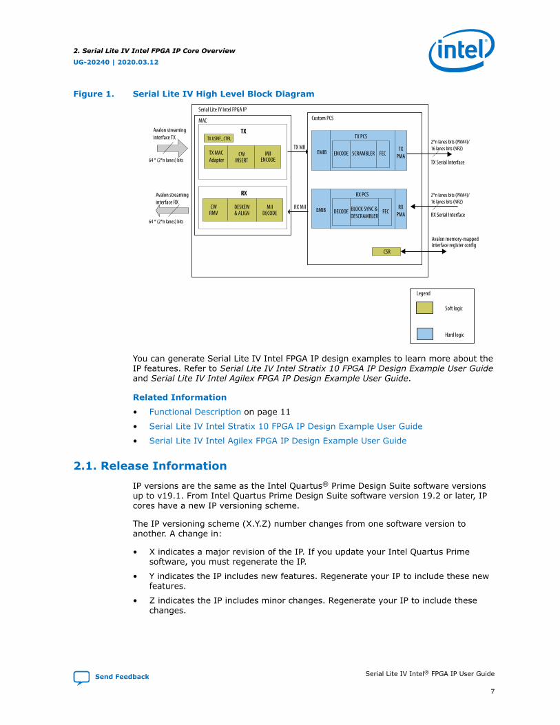
Figure 1. Serial Lite IV High Level Block Diagram
CSR
TX MAC Adapter
TX USRIF_CTRL
Avalon streaminginterface TX
Avalon streaminginterface RX
TX
RX
CWINSERT
MIIENCODE
Avalon memory-mappedinterface register config
TX PCS
ENCODE FECSCRAMBLERTX
PMA
RX PCS
DECODE FECBLOCK SYNC &DESCRAMBLER
RXPMA
DESKEW& ALIGN
CWRMV
MIIDECODE RX Serial Interface
TX Serial Interface
EMIB
EMIB
64 * (2*n lanes) bits
64 * (2*n lanes) bits
2*n lanes bits (PAM4)/16 lanes bits (NRZ)
2*n lanes bits (PAM4)/16 lanes bits (NRZ)
Serial Lite IV Intel FPGA IP
MAC Custom PCS
TX MII
RX MII
Soft logic
Hard logic
Legend
You can generate Serial Lite IV Intel FPGA IP design examples to learn more about theIP features. Refer to Serial Lite IV Intel Stratix 10 FPGA IP Design Example User Guideand Serial Lite IV Intel Agilex FPGA IP Design Example User Guide.
Related Information
• Functional Description on page 11
• Serial Lite IV Intel Stratix 10 FPGA IP Design Example User Guide
• Serial Lite IV Intel Agilex FPGA IP Design Example User Guide
2.1. Release Information
IP versions are the same as the Intel Quartus® Prime Design Suite software versionsup to v19.1. From Intel Quartus Prime Design Suite software version 19.2 or later, IPcores have a new IP versioning scheme.
The IP versioning scheme (X.Y.Z) number changes from one software version toanother. A change in:
• X indicates a major revision of the IP. If you update your Intel Quartus Primesoftware, you must regenerate the IP.
• Y indicates the IP includes new features. Regenerate your IP to include these newfeatures.
• Z indicates the IP includes minor changes. Regenerate your IP to include thesechanges.
2. Serial Lite IV Intel FPGA IP Core Overview
UG-20240 | 2020.03.12
Send Feedback Serial Lite IV Intel® FPGA IP User Guide
7

Table 3. Serial Lite IV Intel FPGA IP Release Information
Item Description
IP Version 1.2.0
Intel Quartus Prime Version 19.4
Release Date December 2019
Ordering Code IP-SLITE4
2.2. Supported Features
The following table lists the features available in Serial Lite IV Intel FPGA IP:
Table 4. Serial Lite IV Intel FPGA IP Features
Feature Description
Data Transfer • Supports up to 56 Gbps per lane with a maximum ofeight PAM4 lanes in a single link.
• Supports up to 28 Gbps per lane with a maximum of 16NRZ lanes.
• Supports continuous streaming (Basic) or packet (Full)modes.
• Supports low overhead frame packets.• Supports byte granularity transfer for every burst size.• Supports user-initiated or automatic lane alignment.• Supports programmable alignment period.
PCS • Uses hard IP logic that interfaces seamlessly to IntelStratix 10 and Intel Agilex E-tile transceivers for softlogic resource reduction.
• Supports PAM4 modulation mode for 100GBASE-KP4specification. RS-FEC is always enabled in thismodulation mode.
• Supports NRZ with optional RS-FEC modulation mode.• Supports 64b/66b encoding decoding.
Error Detection and Handling • Supports CRC error checking on TX and RX data paths.• Supports RX link error checking.• Supports RX PCS error detection.
Interfaces • Supports only full duplex packet transfer withindependent links.
• Uses point-to-point interconnect to multiple FPGAdevices with low transfer latency.
• Supports user-defined commands.
2.3. IP Version Support Level
The following are the supported Intel Quartus Prime software versions and devices forthe Serial Lite IV Intel FPGA IP.
Table 5. IP Version and Support Level
Intel Quartus Prime Device IP Version Simulation Compilation Hardware Design
19.4 Intel Stratix 10 E-tile transceivers 1.2.0 √ √ √
Intel Agilex E-tile transceivers 1.2.0 √ √ √
2. Serial Lite IV Intel FPGA IP Core Overview
UG-20240 | 2020.03.12
Serial Lite IV Intel® FPGA IP User Guide Send Feedback
8
2.4. Device Speed Grade Support
The Serial Lite IV Intel FPGA IP supports the following speed grades for Intel Stratix10 and Intel Agilex E-tile devices:
• Transceiver speed grade: -1, -2, and -3
• Core speed grade: -1, -2, and -3
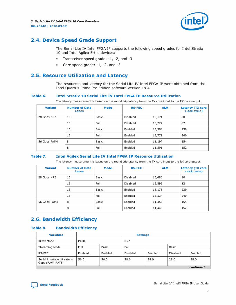
2.5. Resource Utilization and Latency
The resources and latency for the Serial Lite IV Intel FPGA IP were obtained from theIntel Quartus Prime Pro Edition software version 19.4.
Table 6. Intel Stratix 10 Serial Lite IV Intel FPGA IP Resource UtilizationThe latency measurement is based on the round trip latency from the TX core input to the RX core output.
Variant Number of DataLanes
Mode RS-FEC ALM Latency (TX coreclock cycle)
28 Gbps NRZ 16 Basic Disabled 16,171 80
16 Full Disabled 16,724 82
16 Basic Enabled 15,383 239
16 Full Enabled 15,771 240
56 Gbps PAM4 8 Basic Enabled 11,197 154
8 Full Enabled 11,591 152
Table 7. Intel Agilex Serial Lite IV Intel FPGA IP Resource UtilizationThe latency measurement is based on the round trip latency from the TX core input to the RX core output.
Variant Number of DataLanes
Mode RS-FEC ALM Latency (TX coreclock cycle)
28 Gbps NRZ 16 Basic Disabled 16,480 80
16 Full Disabled 16,896 82
16 Basic Enabled 15,173 239
16 Full Enabled 15,534 240
56 Gbps PAM4 8 Basic Enabled 11,356 154
8 Full Enabled 11,448 152
2.6. Bandwidth Efficiency
Table 8. Bandwidth Efficiency
Variables Settings
XCVR Mode PAM4 NRZ
Streaming Mode Full Basic Full Basic
RS-FEC Enabled Enabled Disabled Enabled Disabled Enabled
Serial interface bit rate inGbps (RAW_RATE)
56.0 56.0 28.0 28.0 28.0 28.0
continued...
2. Serial Lite IV Intel FPGA IP Core Overview
UG-20240 | 2020.03.12
Send Feedback Serial Lite IV Intel® FPGA IP User Guide
9

Variables Settings
Burst size of a transfer innumber of word(BURST_SIZE)(1)
2,048 4,194,304 2,048 2,048 4,194,304 4,194,304
Alignment period in clockcycle(SRL4_ALIGN_PERIOD)
4,096 4,096 4,096 4,096 4,096 4,096
64/66b encode 0.96969697 0.96969697 0.96969697 0.96969697 0.96969697 0.96969697
Overhead of a burst sizein number of word(BURST_SIZE_OVHD)
2 0 2(2) 2(2) 0(3) 0(3)
Alignment marker periodin clock cycle(ALIGN_MARKER_PERIOD)
81,915 81,915 81,916 81,916 81,916 81,916
Alignment marker width inclock cycle(ALIGN_MARKER_WIDTH)
5 5 0 4 0 4
Bandwidth efficiency(4) 0.96821788 0.96916433 0.96827698 0.96822967 0.96922348 0.96917616
Effective rate (Gbps) (5) 54.2202012 54.27320236 27.11175544 27.11043076 27.13825744 27.13693248
Maximum user clockfrequency (MHz) (6)
423.59532225 424.00939437 423.62117875 423.6004806 424.0352725 424.01457
Related Information
Link Rate and Bandwidth Efficiency Calculation on page 32
(1) The BURST_SIZE for Basic mode approaches infinity, hence a large number is used.
(2) In Full mode, the BURST_SIZE_OVHD size is inclusive of the START/END paired Control Wordsin a data stream.
(3) For Basic mode, BURST_SIZE_OVHD is 0 because there is no START/END during streaming.
(4) Refer to Link Rate and Bandwidth Efficiency Calculation for bandwidth efficiency calculation.
(5) Refer to Link Rate and Bandwidth Efficiency Calculation for effective rate calculation.
(6) Refer to Link Rate and Bandwidth Efficiency Calculation for maximum user clock frequencycalculation.
2. Serial Lite IV Intel FPGA IP Core Overview
UG-20240 | 2020.03.12
Serial Lite IV Intel® FPGA IP User Guide Send Feedback
10
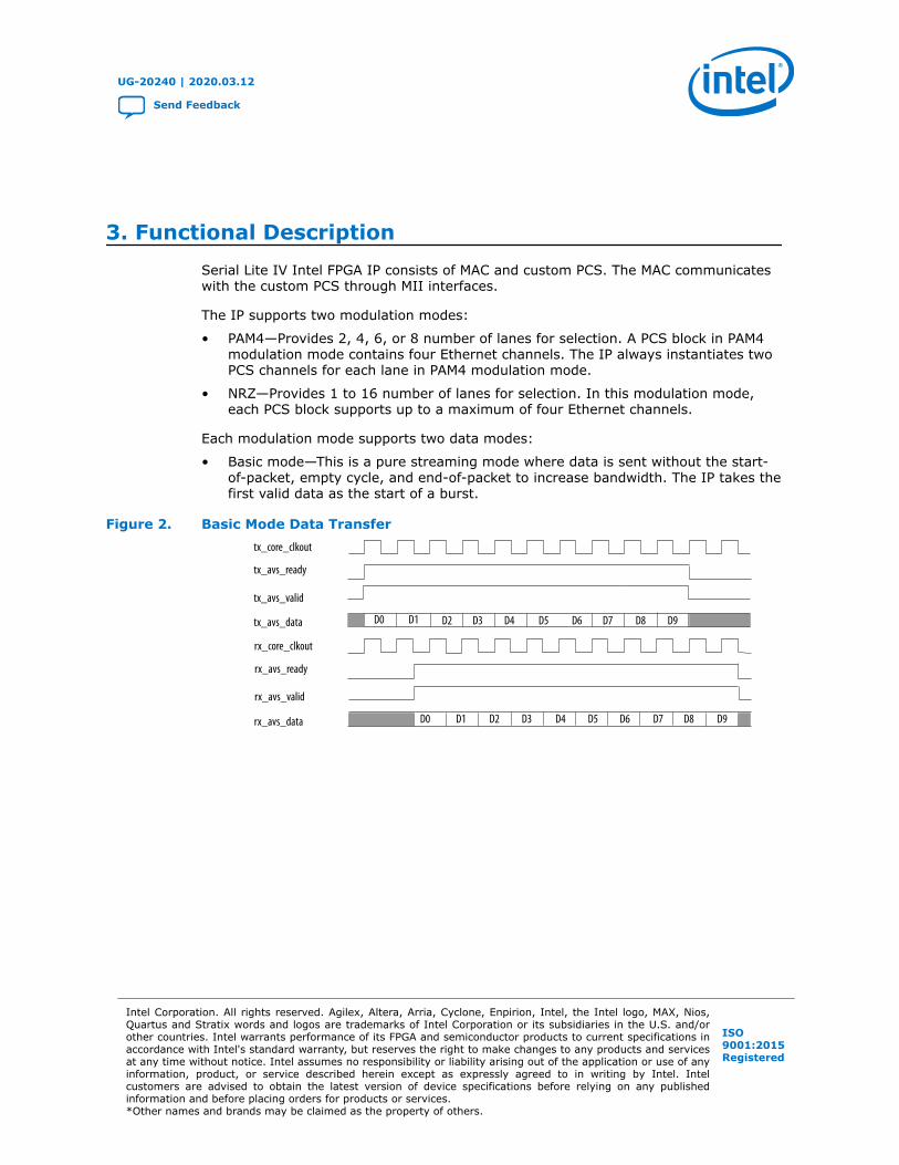
3. Functional DescriptionSerial Lite IV Intel FPGA IP consists of MAC and custom PCS. The MAC communicateswith the custom PCS through MII interfaces.
The IP supports two modulation modes:
• PAM4—Provides 2, 4, 6, or 8 number of lanes for selection. A PCS block in PAM4modulation mode contains four Ethernet channels. The IP always instantiates twoPCS channels for each lane in PAM4 modulation mode.
• NRZ—Provides 1 to 16 number of lanes for selection. In this modulation mode,each PCS block supports up to a maximum of four Ethernet channels.
Each modulation mode supports two data modes:
• Basic mode—This is a pure streaming mode where data is sent without the start-of-packet, empty cycle, and end-of-packet to increase bandwidth. The IP takes thefirst valid data as the start of a burst.
Figure 2. Basic Mode Data Transfertx_core_clkout
tx_avs_valid
tx_avs_data D0 D1 D2 D3 D4 D5 D6 D7
rx_core_clkout
rx_avs_data D0 D1 D2 D3 D4 D5 D6 D7
rx_avs_valid
tx_avs_ready
rx_avs_ready
D8 D9
D8 D9
UG-20240 | 2020.03.12
Send Feedback
Intel Corporation. All rights reserved. Agilex, Altera, Arria, Cyclone, Enpirion, Intel, the Intel logo, MAX, Nios,Quartus and Stratix words and logos are trademarks of Intel Corporation or its subsidiaries in the U.S. and/orother countries. Intel warrants performance of its FPGA and semiconductor products to current specifications inaccordance with Intel's standard warranty, but reserves the right to make changes to any products and servicesat any time without notice. Intel assumes no responsibility or liability arising out of the application or use of anyinformation, product, or service described herein except as expressly agreed to in writing by Intel. Intelcustomers are advised to obtain the latest version of device specifications before relying on any publishedinformation and before placing orders for products or services.*Other names and brands may be claimed as the property of others.
ISO9001:2015Registered

• Full mode—This is the packet mode data transfer. In this mode, the IP sends aburst and a sync cycle at the start and the end of a packet as delimiters.
Figure 3. Full Mode Data Transfertx_core_clkout
tx_avs_valid
tx_avs_data D0 D1 D2 D3 D4 D5 D6 D7
tx_avs_startofpacket
tx_avs_endofpacket
rx_core_clkout
rx_avs_startofpacket
rx_avs_endofpacket
rx_avs_data D0 D1 D2 D3 D4 D5 D6 D7
rx_avs_valid
tx_avs_ready
rx_avs_ready
D8 D9
D8 D9
Related Information
• Serial Lite IV Intel FPGA IP Core Overview on page 6
• Serial Lite IV Intel Stratix 10 FPGA IP Design Example User Guide
• Serial Lite IV Intel Agilex FPGA IP Design Example User Guide
• E-Tile Transceiver PHY User Guide
• Ethernet Link Inspector User Guide for Intel Stratix 10 DevicesInformation about the Ethernet Link Inspector, an inspection tool that cancontinuously monitor an Ethernet link.
3.1. TX Datapath
The TX datapath consists of the following components:
• MAC adapter
• Control word insertion block
• CRC
• MII encoder
• PCS block
• PMA block
3. Functional Description
UG-20240 | 2020.03.12
Serial Lite IV Intel® FPGA IP User Guide Send Feedback
12

Figure 4. TX Datapath
Avalon StreamingInterface
MAC Adapter
MII Interface
From user logic
Control Word Insertion
CRC
MII Encoder
TX MAC
Custom PCS
TX Serial Interface
To Other FPGA Device
PCS and PMA
3.1.1. TX MAC Adapter
The function of the TX MAC adapter is to control the data transmission to the userlogic using the Avalon streaming interface. This block supports user-definedinformation transmission and flow control.
Transferring User-defined Information
In Full mode, the IP provides the tx_is_usr_cmd signal which lets you initiate user-defined information cycle such as XOFF/XON transmission to the user logic. You caninitiate the user-defined information transmission cycle by asserting this signal andtransfer the information using tx_avs_data along with the assertion oftx_avs_startofpacket and tx_avs_valid signals. The block then deasserts thetx_avs_ready for two cycles.
Note: The user-defined information feature is only available in Full mode.
3. Functional Description
UG-20240 | 2020.03.12
Send Feedback Serial Lite IV Intel® FPGA IP User Guide
13
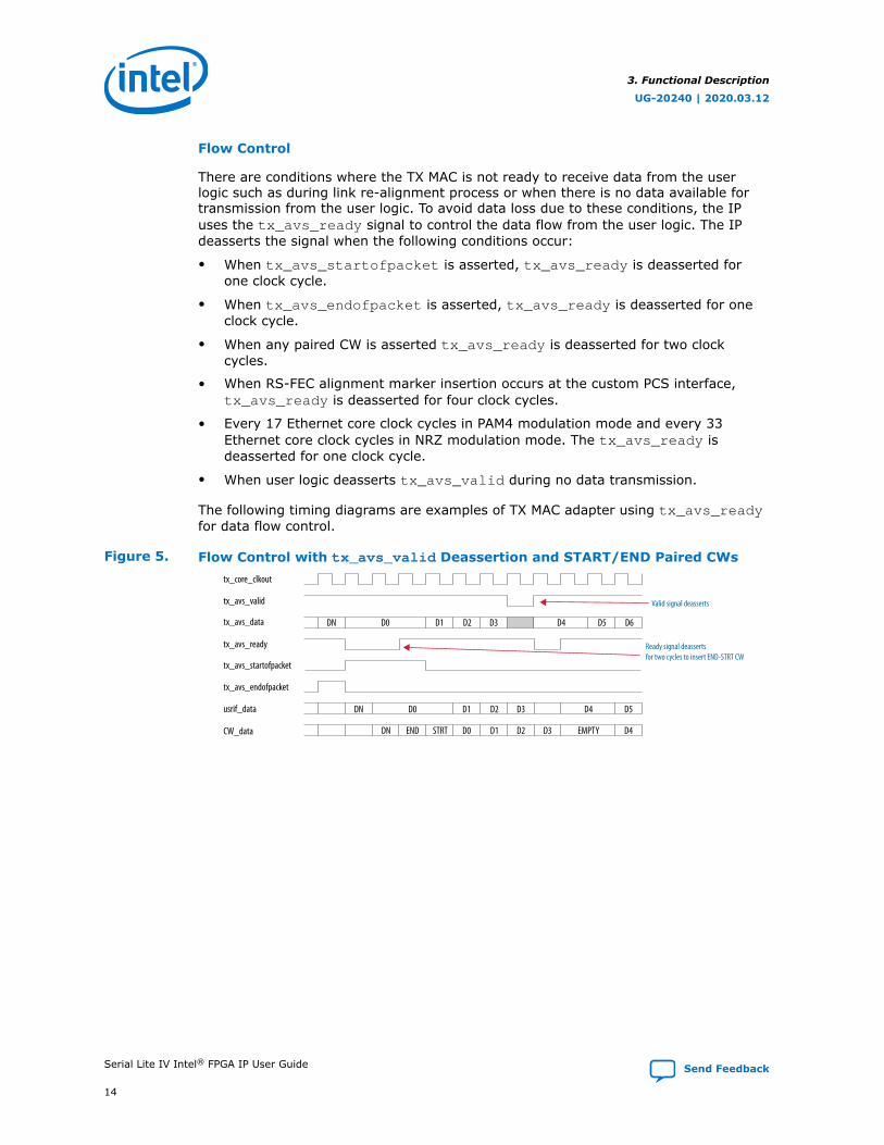
Flow Control
There are conditions where the TX MAC is not ready to receive data from the userlogic such as during link re-alignment process or when there is no data available fortransmission from the user logic. To avoid data loss due to these conditions, the IPuses the tx_avs_ready signal to control the data flow from the user logic. The IPdeasserts the signal when the following conditions occur:
• When tx_avs_startofpacket is asserted, tx_avs_ready is deasserted forone clock cycle.
• When tx_avs_endofpacket is asserted, tx_avs_ready is deasserted for oneclock cycle.
• When any paired CW is asserted tx_avs_ready is deasserted for two clockcycles.
• When RS-FEC alignment marker insertion occurs at the custom PCS interface,tx_avs_ready is deasserted for four clock cycles.
• Every 17 Ethernet core clock cycles in PAM4 modulation mode and every 33Ethernet core clock cycles in NRZ modulation mode. The tx_avs_ready isdeasserted for one clock cycle.
• When user logic deasserts tx_avs_valid during no data transmission.
The following timing diagrams are examples of TX MAC adapter using tx_avs_readyfor data flow control.
Figure 5. Flow Control with tx_avs_valid Deassertion and START/END Paired CWs
DN D0 D1 D2 D3 D4
D0DN D1 D2 D3 D4 D5
Valid signal deasserts
Ready signal deasserts for two cycles to insert END-STRT CW
D5 D6
END STRTDN D0 D1 D2 D3 EMPTY D4
tx_core_clkout
tx_avs_valid
tx_avs_data
tx_avs_ready
tx_avs_startofpacket
tx_avs_endofpacket
usrif_data
CW_data
3. Functional Description
UG-20240 | 2020.03.12
Serial Lite IV Intel® FPGA IP User Guide Send Feedback
14

Figure 6. Flow Control with Alignment Marker Insertiontx_core_clkout
tx_avs_valid
tx_avs_data
tx_avs_ready
tx_avs_startofpacket
tx_avs_endofpacket
usrif_data
CW_data
CRC_data
MII_data
i_sl_tx_mii_valid
i_sl_tx_mii_d[63:0]
i_sl_tx_mii_c[7:0]
i_sl_tx_mii_am
i_sl_tx_mii_am_pre3
DN-5 DN-4 DN-3 DN-2 DN-1 DN+1D0
0 1 2 3 4
DN-1 DN+1DN
0 1 2 3 4
0x0
0 1 2 3 4
DN DN DN DN DN DN DN+1DN-1
DN-1 DN DN DN DN DN DN DN+1
DN-1 DN DN DN DN DN DN DN+1
DN-1 DN DN DN DN DN DN DN+1
Figure 7. Flow Control with START/END Paired CW Coincide with Alignment MarkerInsertion
DN-5
tx_core_clkout
tx_avs_valid
tx_avs_data
tx_avs_ready
tx_avs_startofpacket
tx_avs_endofpacket
usrif_data
CW_data
CRC_data
MII_data
i_sl_tx_mii_valid
i_sl_tx_mii_d[63:0]
i_sl_tx_mii_c[7:0]
i_sl_tx_mii_am
i_sl_tx_mii_am_pre3
DN-4 DN-3 DN-2 DN-1
DN-1 DN-1 DN-1 DN-1 DN-1 END STRT D0DN-1
DN-1 DN-1 DN-1 DN-1 DN-1 DN-1 END STRT D0
DN-1 DN-1 DN-1 DN-1 DN-1 DN-1 END STRT D0
DN-1 DN-1 DN-1 DN-1 DN-1 DN-1 END STRT D0
D0
0 1 2 3 4 5 6
DN-1
0x0
0 1 2 3 4
0 1 2 3 4
END D0STRT
3.1.2. CW Insertion
The Serial Lite IV Intel FPGA IP constructs CW based on the input signals from theuser logic. The CW are to indicates packet delimiters, transmission status informationor user data to the PCS block and they are derived from XGMII control codes.
The following table shows the description of the supported CW:
3. Functional Description
UG-20240 | 2020.03.12
Send Feedback Serial Lite IV Intel® FPGA IP User Guide
15

Table 9. Description of Supported CW
CW Number of Words (1 word= 64 bits)
In-band Description
START 1 Yes Start of data delimiter
END 1 Yes End of data delimiter
ALIGN 2 Yes Control word for RXalignment
EMPTY_CYC 2 Yes Empty cycle in a datatransfer
IDLE 1 No IDLE (out of band)
DATA 1 Yes Payload
Table 10. CW Field Description
Field Description
RSVD Reserved field. May be used for future extension. Tied to 0.
num_valid_bytes_eob Number of valid bytes in the last word (64-bit). This is a 3-bit value.• 3'b000: 8 bytes• 3'b001: 1 byte• 3'b010: 2 bytes• 3'b011: 3 bytes• 3'b100: 4 bytes• 3'b101: 5 bytes• 3'b110: 6 bytes• 3'b111: 7 bytes
EMPTY Number of non-valid words at the end of a burst.
eop Indicates the RX Avalon streaming interface to assert anend-of-packet signal.
sop Indicates the RX Avalon streaming interface to assert astart-of-packet signal.
seop Indicates the RX Avalon streaming interface to assert astart-of-packet and an end-of-packet in the same cycle.
align Check RX alignment.
CRC32 The values of computed CRC.
usr Indicates that the control word contains user-definedinformation.
3. Functional Description
UG-20240 | 2020.03.12
Serial Lite IV Intel® FPGA IP User Guide Send Feedback
16
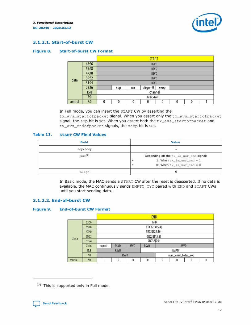
3.1.2.1. Start-of-burst CW
Figure 8. Start-of-burst CW Format
63:5655:4847:4039:3231:2423:16 sop usr align=0 seop15:87:0
control 7:0 0 0 0 0 0 0 0 1
RSVDRSVD
channel'hFB(START)
START
data
RSVDRSVDRSVD
In Full mode, you can insert the START CW by asserting thetx_avs_startofpacket signal. When you assert only the tx_avs_startofpacketsignal, the sop bit is set. When you assert both the tx_avs_startofpacket andtx_avs_endofpacket signals, the seop bit is set.
Table 11. START CW Field Values
Field Value
sop/seop 1
usr(7) Depending on the tx_is_usr_cmd signal:• 1: When tx_is_usr_cmd = 1• 0: When tx_is_usr_cmd = 0
align 0
In Basic mode, the MAC sends a START CW after the reset is deasserted. If no data isavailable, the MAC continuously sends EMPTY_CYC paired with END and START CWsuntil you start sending data.
3.1.2.2. End-of-burst CW
Figure 9. End-of-burst CW Format
CRC32[31:24]63:5655:4847:4039:3231:2423:16 eop=1 RSVD RSVD RSVD15:8 RSVD7:0
control 7:0 1 0 0 0 0 0 0 0
END'hFD
data
RSVD
num_valid_bytes_eobRSVDEMPTY
CRC32[23:16]CRC32[15:8]CRC32[7:0]
(7) This is supported only in Full mode.
3. Functional Description
UG-20240 | 2020.03.12
Send Feedback Serial Lite IV Intel® FPGA IP User Guide
17

The MAC inserts the END CW when the tx_avs_endofpacket is asserted. The ENDCW contains the number of valid bytes at the last word and the CRC information.
The CRC value is a 32-bit CRC result for the data between the START CW and theword before the END CW.
The following table shows the values of the fields in END CW.
Table 12. END CW Field Values
Field Value
eop 1
CRC32 CRC32 computed value.
num_valid_bytes_eob Number of valid bytes at the last word.
3.1.2.3. Alignment Paired CW
Figure 10. Alignment Paired CW Format
63:5655:4847:4039:3231:2423:16 eop=0 sop=0 usr=0 align=1 seop=015:87:0
control 7:0 0 0 0 0 0 0 0 1
63:5655:4847:4039:3231:2423:16 eop=0 RSVD RSVD RSVD15:87:0
control 7:0 1 0 0 0 0 0 0 0
RSVD
START
data
RSVDRSVDRSVDRSVDRSVD
RSVD'hFB
ALIGN CW Pair with START/END
64+8 bits XGMII Interface
data
RSVDRSVD
64+8 bits XGMII InterfaceEND'hFDRSVDRSVDRSVDRSVD
63:5655:4847:4039:3231:2423:16 eop=0 RSVD RSVD RSVD15:87:0
control 7:0 1 0 0 0 0 0 0 0
63:5655:4847:4039:3231:2423:16 eop=0 sop=0 usr=0 align=1 seop=015:87:0
control 7:0 0 0 0 0 0 0 0 1
64+8 bits XGMII Interface
START
data
RSVDRSVDRSVDRSVDRSVD
RSVD'hFB
ALIGN CW Pair with END/START
64+8 bits XGMII Interface
END
data
'hFDRSVDRSVDRSVDRSVD
RSVDRSVDRSVD
The ALIGN CW is a paired CW with START/END or END/START CWs. You can insert theALIGN paired CW by either asserting the tx_link_reinit signal, set the AlignmentPeriod counter, or initiating a reset. When the ALIGN paired CW is inserted, the alignfield is set to 1 to initiate the receiver alignment block to check data alignment acrossall lanes.
3. Functional Description
UG-20240 | 2020.03.12
Serial Lite IV Intel® FPGA IP User Guide Send Feedback
18

Table 13. ALIGN CW Field Values
Field Value
align 1
eop 0
sop 0
usr 0
seop 0
3.1.2.4. Empty-cycle CW
Figure 11. Empty-cycle CW Format
63:5655:4847:4039:3231:2423:16 eop=0 RSVD RSVD RSVD15:8 RSVD7:0
control 7:0 1 0 0 0 0 0 0 0
63:5655:4847:4039:3231:2423:16 sop=0 usr=0 align=0 seop=015:87:0
control 7:0 0 0 0 0 0 0 0 1
END
data
'hFDRSVDRSVDRSVDRSVD
RSVD
'hFB
64+8 bits XGMII InterfaceSTART
data
RSVDRSVDRSVDRSVDRSVD
RSVD
RSVDRSVD RSVD
EMPTY_CYC Pair with END/START
64+8 bits XGMII Interface
When you deassert tx_avs_valid for two clock cycles during a burst, the MACinserts an EMPTY_CYC CW paired with END/START CWs. You can use this CW whenthere is no data available for transmission momentarily.
When you deassert tx_avs_valid for one cycle, the IP deasserts tx_avs_valid fortwice the period of tx_avs_valid deassertion to generate a pair of END/START CWs.
Table 14. EMPTY_CYC CW Field Values
Field Value
align 0
eop 0
continued...
3. Functional Description
UG-20240 | 2020.03.12
Send Feedback Serial Lite IV Intel® FPGA IP User Guide
19

Field Value
sop 0
usr 0
seop 0
3.1.2.5. Idle CW
Figure 12. Idle CW Format
63:5655:4847:4039:3231:2423:1615:87:0
control 7:0 1 1 1 1 1 1 1 1'h07
IDLE CW
data
'h07'h07'h07'h07'h07'h07'h07
The MAC insert the IDLE CW when there is no transmission. During this period, thetx_avs_valid signal is low.
You can use the IDLE CW when a burst transfer has completed or the transmission isin an idle state.
3.1.2.6. Data Word
The data word is the payload of a packet. The XGMII control bits are all set to 0 indata word format.
Figure 13. Data Word Format
63:5655:4847:4039:3231:2423:1615:87:0
control 7:0 0 0 0 0 0 0 0 0
data
user data 7user data 6user data 5user data 4user data 3
user data 0
user data 2user data 1
DATA WORD64+8 bits XGMII Interface
3.1.3. TX CRC
You can enable the TX CRC block using the Enable CRC parameter in the IPParameter Editor. This feature is supported in both Basic and Full modes.
3. Functional Description
UG-20240 | 2020.03.12
Serial Lite IV Intel® FPGA IP User Guide Send Feedback
20

The MAC adds the CRC value to the END CW by asserting the tx_avs_endofpacketsignal. In the BASIC mode, only the ALIGN CW paired with END CW contains a validCRC field.
The TX CRC block interfaces with the TX Control Word Insertion and TX MII Encodeblock. The TX CRC block computes the CRC value for 64-bit value per-cycle datastarting from the START CW up to the END CW.
You can assert the crc_error_inject signal to intentionally corrupt data in aspecific lane to create CRC errors.
3.1.4. TX MII Encoder
The TX MII encoder handles the packet transmission from the MAC to the TX PCS.
In PAM4 mode, a custom PCS always contains four Ethernet channels. Therefore theMII bus data pattern in PAM4 mode is different than the MII bus data pattern in NRZmode. The following figure shows the data pattern on the 8-bit MII bus in PAM4modulation mode. The START and END CW appear once in every four MII lanes.
Figure 14. PAM4 Modulation Mode MII Data Pattern
SOP_CW
DATA_DUMMY
DATA_DUMMY
DATA_DUMMY
DATA_DUMMY
SOP_CW
DATA_DUMMY
DATA_DUMMY
DATA_1
DATA_2
DATA_3
DATA_4
DATA_5
DATA_6
DATA_7
DATA_8
DATA_9
DATA_10
DATA_11
DATA_12
DATA_13
DATA_14
DATA_15
DATA_16
DATA_17
DATA_18
DATA_19
DATA_20
DATA_21
DATA_22
DATA_23
DATA_24
EOP_CW
IDLE
EOP_CW
IDLE
IDLE
IDLE
IDLE
IDLE
CYCLE 1 CYCLE 2 CYCLE 3 CYCLE 4 CYCLE 5
The following figure shows the data pattern on the 8-bit MII bus in NRZ modulationmode. The START and END CW appear in every MII lanes.
3. Functional Description
UG-20240 | 2020.03.12
Send Feedback Serial Lite IV Intel® FPGA IP User Guide
21
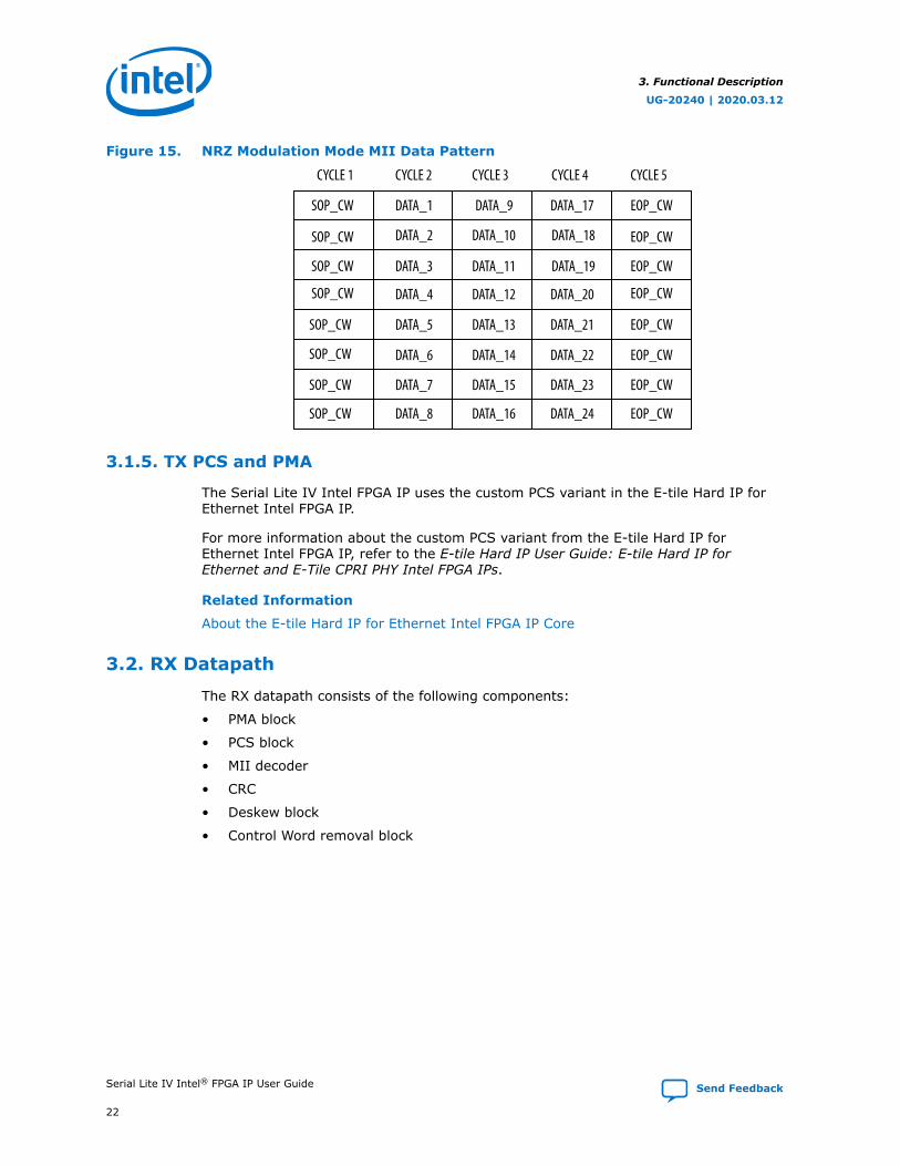
Figure 15. NRZ Modulation Mode MII Data Pattern
SOP_CW
SOP_CW
DATA_1
DATA_2
DATA_3
DATA_4
DATA_5
DATA_6
DATA_7
DATA_8
DATA_9
DATA_10
DATA_11
DATA_12
DATA_13
DATA_14
DATA_15
DATA_16
DATA_17
DATA_18
DATA_19
DATA_20
DATA_21
DATA_22
DATA_23
DATA_24
EOP_CW
EOP_CW
CYCLE 1 CYCLE 2 CYCLE 3 CYCLE 4 CYCLE 5
SOP_CW EOP_CW
SOP_CW
SOP_CW
SOP_CW
SOP_CW
SOP_CW
EOP_CW
EOP_CW
EOP_CW
EOP_CW
EOP_CW
3.1.5. TX PCS and PMA
The Serial Lite IV Intel FPGA IP uses the custom PCS variant in the E-tile Hard IP forEthernet Intel FPGA IP.
For more information about the custom PCS variant from the E-tile Hard IP forEthernet Intel FPGA IP, refer to the E-tile Hard IP User Guide: E-tile Hard IP forEthernet and E-Tile CPRI PHY Intel FPGA IPs.
Related Information
About the E-tile Hard IP for Ethernet Intel FPGA IP Core
3.2. RX Datapath
The RX datapath consists of the following components:
• PMA block
• PCS block
• MII decoder
• CRC
• Deskew block
• Control Word removal block
3. Functional Description
UG-20240 | 2020.03.12
Serial Lite IV Intel® FPGA IP User Guide Send Feedback
22

Figure 16. RX Datapath
Avalon Streaming Interface
MII Interface
To user logic
Control Word Removal
Deskew
MII Decoder
PCS and PMA
RX MAC
Custom PCS
RX Serial Interface
From Other FPGA Device
CRC
3.2.1. RX PCS and PMA
The Serial Lite IV Intel FPGA IP uses the custom PCS variant in the E-tile Hard IP forEthernet Intel FPGA IP.
For more information about the custom PCS variant from the E-tile Hard IP forEthernet Intel FPGA IP, refer to the E-tile Hard IP User Guide: E-tile Hard IP forEthernet and E-Tile CPRI PHY Intel FPGA IPs.
Related Information
About the E-tile Hard IP for Ethernet Intel FPGA IP Core
3.2.2. RX MII Decoder
This block identifies if incoming data contains control word and alignment markers.
The RX MII decoder outputs data in the form of 1-bit valid, 1-bit marker indicator, 1-bit control indicator, and 64-bit data per lane.
3. Functional Description
UG-20240 | 2020.03.12
Send Feedback Serial Lite IV Intel® FPGA IP User Guide
23

3.2.3. RX CRC
You can enable the TX CRC block using the Enable CRC parameter in the IPParameter Editor. This feature is supported in both Basic and Full modes.
The RX CRC block interfaces with the RX Control Word Removal and RX MII Decoderblocks. The IP asserts rx_crc_error signal when a CRC error occurs.
The IP deasserts the rx_crc_error at every new burst. It is an output to the userlogic for user logic error handling.
3.2.4. RX Deskew
The RX deskew block detects the alignment markers for each lane and re-aligns thedata before sending it to the RX CW removal block.
You can choose to let the IP core to align the data for each lane automatically when analignment error occurs by setting the Enable Auto Alignment parameter in the IPparameter Editor. If you disable the automatic alignment feature, the IP core assertsthe rx_error signal to indicate alignment error. You must assert therx_link_reinit to initiate the lane alignment process when a lane alignment erroroccurs.
The RX deskew detects the alignment markers based on a state machine. Thefollowing diagram shows the states in the RX deskew block.
3. Functional Description
UG-20240 | 2020.03.12
Serial Lite IV Intel® FPGA IP User Guide Send Feedback
24

Figure 17. RX Deskew Lane Alignment State Machine with Auto Alignment Enabled FlowChart
Start
IDLE
WAIT
Reset = 1yes
no
All PCS lanes ready?
yes
no
All sync markersdetected?
yes
no Timeout?yes
no
End
ALIGN
Lost of alignment?yes
no
3. Functional Description
UG-20240 | 2020.03.12
Send Feedback Serial Lite IV Intel® FPGA IP User Guide
25
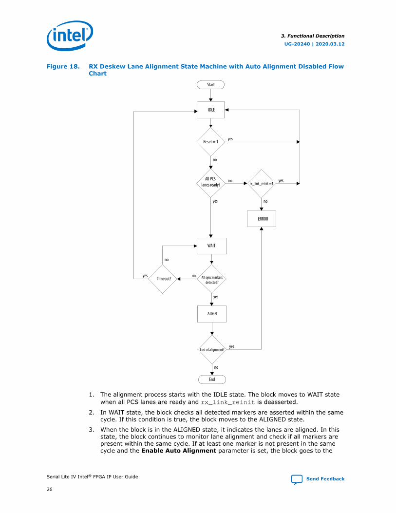
Figure 18. RX Deskew Lane Alignment State Machine with Auto Alignment Disabled FlowChart
Start
IDLE
WAIT
Reset = 1yes
no
All PCS lanes ready?
yes
norx_link_reinit =1
yes
no
All sync markersdetected?
yes
noTimeout?
yes
no
End
ALIGN
Lost of alignment?yes
no
ERROR
1. The alignment process starts with the IDLE state. The block moves to WAIT statewhen all PCS lanes are ready and rx_link_reinit is deasserted.
2. In WAIT state, the block checks all detected markers are asserted within the samecycle. If this condition is true, the block moves to the ALIGNED state.
3. When the block is in the ALIGNED state, it indicates the lanes are aligned. In thisstate, the block continues to monitor lane alignment and check if all markers arepresent within the same cycle. If at least one marker is not present in the samecycle and the Enable Auto Alignment parameter is set, the block goes to the
3. Functional Description
UG-20240 | 2020.03.12
Serial Lite IV Intel® FPGA IP User Guide Send Feedback
26

IDLE state to re-initialize the alignment process. If Enable Auto Alignment is notset and at least one marker is not present in the same cycle, the block goes toERROR state and waits for the user logic to assert rx_link_reinit signal toinitiate lane alignment process.
Figure 19. Lane Realignment with Enable Auto Alignment Enabled
rx_core_clk
ALGNED ALGNEDIDLE
AUTO_ALIGN = 1
WAIT
rx_link_up
rx_link_reinit
and_all_markers
Deskew State
Figure 20. Lane Realignment with Enable Auto Alignment Disabled
rx_core_clk
ALGNED ALGNEDERROR IDLE WAIT
AUTO_ALIGN = 0
rx_link_up
rx_link_reinit
and_all_markers
Deskew State
3.2.5. RX CW Removal
This block decodes the CW and sends data to the user logic using the Avalonstreaming interface after the removal of the CW.
When there is no valid data available, the RX CW removal block deasserts therx_avs_valid signal.
In FULL mode, if the user bit is set, this block asserts the rx_is_usr_cmd signal andthe data in the first clock cycle is used as user-defined information or command.
When rx_avs_ready deasserts and rx_avs_valid asserts, the RX CW removalblock generates an error condition to the user logic.
The Avalon streaming signals related to this block are:
• rx_avs_startofpacket
• rx_avs_endofpacket
• rx_avs_channel
• rx_avs_empty
• rx_avs_data
3. Functional Description
UG-20240 | 2020.03.12
Send Feedback Serial Lite IV Intel® FPGA IP User Guide
27

• rx_avs_valid
• rx_num_valid_bytes_eob
• rx_is_usr_cmd (only available in Full mode)
3.3. Serial Lite IV Intel FPGA IP Clock Architecture
The Serial Lite IV Intel FPGA IP has four clock inputs which generate clocks to differentblocks:
• Transceiver reference clock (xcvr_ref_clk)—Input clock from external clockchips or oscillators which generates clocks for TX MAC, RX MAC, and TX and RXcustom PCS blocks. The IP supports reference clocks provided from separate clockchips or oscillators with a tolerance of ±100 ppm clock variation between thedifferent clock chips or oscillators. Refer to Parameters for supported frequencyrange.
• TX core clock (tx_core_clk)—This clock is derived from transceiver PLL(clk_pll_div64[mid_ch]) in the custom PCS and is used for TX custom PCSinterface and TX MAC. This clock is also an output clock from the IP to connect tothe TX user logic.
• RX core clock (rx_core_clk)—This clock is derived from the transceiver PLL(clk_pll_div64[mid_ch]) in the custom PCS and is used for RX custom PCSinterface, RX deskew FIFO, and RX MAC. This clock is also an output clock fromthe IP to connect to the RX user logic.
• Clock for transceiver reconfiguration interface (reconfig_clk)—input clock fromexternal clock circuits or oscillators which generates clocks for custom PCS andRS-FEC reconfiguration interface in both TX and RX datapaths. The clockfrequency is 100 to 162 MHz. For more about custom PCS and RS-FECreconfiguration interface, refer to E-tile Hard IP User Guide: E-tile Hard IP forEthernet and E-Tile CPRI PHY Intel FPGA IPs.
The following block diagram shows Serial Lite IV Intel FPGA IP clock domains and theconnections within the IP.
3. Functional Description
UG-20240 | 2020.03.12
Serial Lite IV Intel® FPGA IP User Guide Send Feedback
28

Figure 21. Serial Lite IV Intel FPGA IP Clock Architecture
Avalon streaminginterface TX data
tx_core_clkout(connect to user logic)
Transceiver reconfiguration interface clock(reconfig_clk)
FPGA2Serial Lite IV Intel FPGA IP
FPGA1
tx_core_clk=clk_pll_div64[mid_ch]
rx_core_clk=clk_pll_div64[mid_ch]
Trans
ceive
r Ref
Clock
(xcvr
_ref_
clk)
Oscillator* Oscillator*
*Use two separate oscillators with a +/-100ppm variation or a single oscillator.
serial_link[(n*2)-1:0]
Legend
FPGA device
RX core clock domain
External device
Transceiver reference clock domain
TX core clock domain
FIFODeskew
Custom PCS
TX MAC RX MAC
FIFODeskew
RX MAC
rx_core_clk=clk_pll_div64[mid_ch]
tx_core_clk=clk_pll_div64[mid_ch]
clk_p
ll_div
64[n
-1:0]
serial_link[(n*2)-1:0]
TX MAC
rx_core_clkout(connect to user logic)
Serial Lite IV Intel FPGA IP
TX
RX
Custom PCS
TX
RX
Data Signals
clk_p
ll_div
64[m
id_ch
]
Oscillator Oscillator
rx_core_clkout(connect to user logic)
tx_core_clkout(connect to user logic)
Trans
ceive
r Ref
Clock
(xcvr
_ref_
clk)
Transceiver reconfiguration interface clock(reconfig_clk)
Avalon streaminginterface RX data
Avalon streaminginterface TX data
Avalon streaminginterface RX data
Related Information
• E-Tile Transceiver PHY User Guide: Ports and Parameters
• E-tile Hard IP User Guide: E-Tile Hard IP for Ethernet and E-Tile CPRI PHY IntelFPGA IPs
More information about Ethernet reconfiguration interfaces.
• Parameters on page 42
3.4. Reset and Link Initialization
The MAC, custom PCS, and reconfiguration blocks have different reset signals:
• TX and RX MAC blocks use tx_core_rst_n and rx_core_rst_n reset signals.
• TX and RX RS-FEC blocks use tx_pcs_fec_phy_reset_n andrx_pcs_fec_phy_reset_n reset signals.
• Reconfiguration block uses the reconfig_reset reset signal.
3. Functional Description
UG-20240 | 2020.03.12
Send Feedback Serial Lite IV Intel® FPGA IP User Guide
29
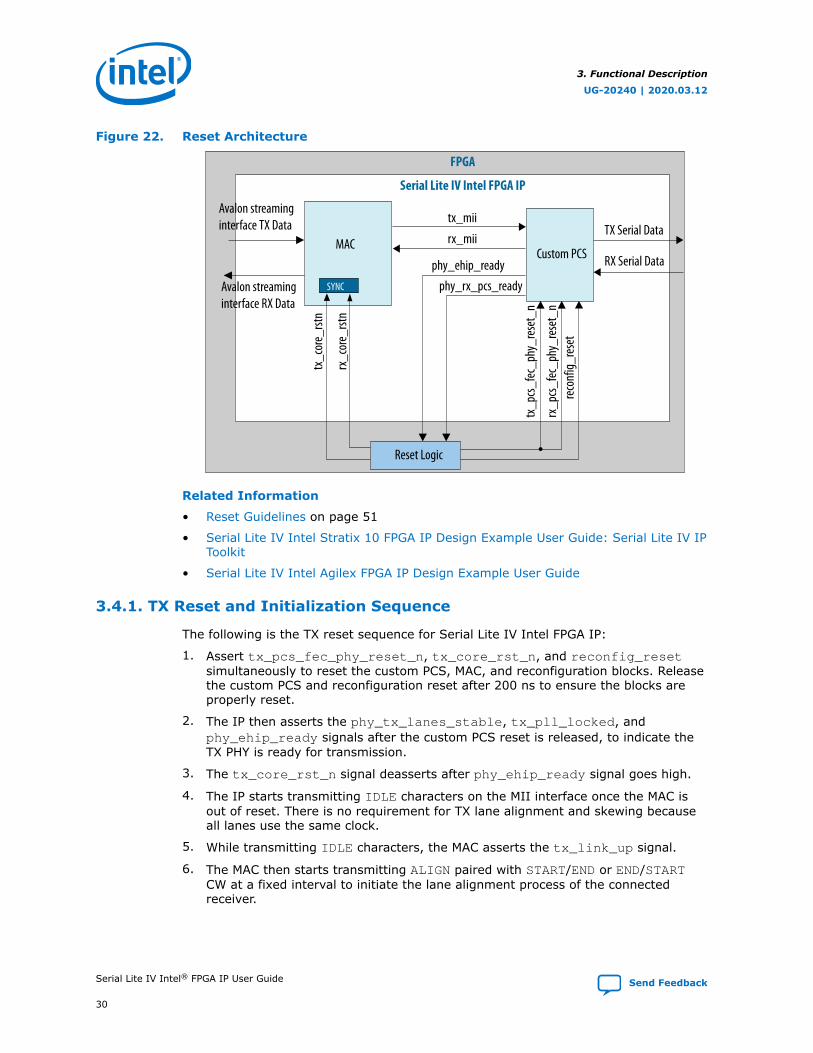
Figure 22. Reset Architecture
MAC
Serial Lite IV Intel FPGA IP
FPGA
Avalon streaminginterface TX Data
Avalon streaming interface RX Data
SYNC
Reset Logic
rx_c
ore_
rstn
tx_c
ore_
rstn
tx_p
cs_fec
_phy
_res
et_n
rx_p
cs_fec
_phy
_res
et_n
reco
nfig_
rese
t
tx_mii
rx_miiTX Serial Data
RX Serial DataCustom PCSphy_ehip_ready
phy_rx_pcs_ready
Related Information
• Reset Guidelines on page 51
• Serial Lite IV Intel Stratix 10 FPGA IP Design Example User Guide: Serial Lite IV IPToolkit
• Serial Lite IV Intel Agilex FPGA IP Design Example User Guide
3.4.1. TX Reset and Initialization Sequence
The following is the TX reset sequence for Serial Lite IV Intel FPGA IP:
1. Assert tx_pcs_fec_phy_reset_n, tx_core_rst_n, and reconfig_resetsimultaneously to reset the custom PCS, MAC, and reconfiguration blocks. Releasethe custom PCS and reconfiguration reset after 200 ns to ensure the blocks areproperly reset.
2. The IP then asserts the phy_tx_lanes_stable, tx_pll_locked, andphy_ehip_ready signals after the custom PCS reset is released, to indicate theTX PHY is ready for transmission.
3. The tx_core_rst_n signal deasserts after phy_ehip_ready signal goes high.
4. The IP starts transmitting IDLE characters on the MII interface once the MAC isout of reset. There is no requirement for TX lane alignment and skewing becauseall lanes use the same clock.
5. While transmitting IDLE characters, the MAC asserts the tx_link_up signal.
6. The MAC then starts transmitting ALIGN paired with START/END or END/STARTCW at a fixed interval to initiate the lane alignment process of the connectedreceiver.
3. Functional Description
UG-20240 | 2020.03.12
Serial Lite IV Intel® FPGA IP User Guide Send Feedback
30

Figure 23. TX Reset and Initialization Timing Diagram
< - ALIGN_CNTR_PERIOD - >
200ns
reconfig_clk
tx_core_rst_n
tx_pcs_fec_phy_reset_n
reconfig_reset
tx_pll_locked
phy_tx_lanes_stable
phy_ehip_ready
tx_link_up
Lane 0 CW(MII)
Lane n-1 CW(MII) alignalign IDLE IDLEIDLE
alignalign IDLE IDLEIDLE
1
1
2
2
2
13
4
5
6
3.4.2. RX Reset and Initialization Sequence
The following is the TX reset sequence for Serial Lite IV Intel FPGA IP:
1. Assert rx_pcs_fec_phy_reset_n, rx_core_rst_n, and reconfig_resetsimultaneously to reset the custom PCS, MAC, and reconfiguration blocks. Releasethe custom PCS and reconfiguration reset after 200 ns to ensure the blocks areproperly reset.
2. The IP then asserts the phy_rx_pcs_readysignal after the custom PCS reset isreleased, to indicate RX PHY is ready for transmission.
3. The rx_core_rst_n signal deasserts after phy_rx_pcs_ready signal goes high.
4. The IP starts the lane alignment process after the RX MAC reset is released andupon receiving ALIGN paired with START/END or END/START CW.
5. The RX deskew block asserts the rx_link_up signal once alignment for all laneshas complete.
6. The IP then asserts the rx_link_up signal to the user logic to indicate that theRX link is ready to start data reception.
Figure 24. RX Reset ad Initialization Timing Diagram
alignalign IDLEIDLE
alignalign IDLEIDLE
< ALIGN_PERIOD >
200ns
reconfig_clk
rx_core_rst_n
rx_pcs_fec_phy_reset_n
reconfig_reset
rx_cdr_lock
rx_block_lock
phy_rx_pcs_ready
rx_link_up
Lane 0 CW(MII)
Lane n-1 CW(MII)
1
1
1
2
3
4
5
3. Functional Description
UG-20240 | 2020.03.12
Send Feedback Serial Lite IV Intel® FPGA IP User Guide
31

3.4.3. PMA Adaptation Flow
The PMA block in the Serial Lite IV Intel FPGA IP uses the same PMA adaptation flowas the E-Tile Hard IP for Ethernet Intel FPGA IP. You may refer to the EthernetAdaptation Flow with Non-external AIB clocking in the E-tile Hard IP User Guide: E-TileHard IP for Ethernet and E-Tile CPRI PHY Intel FPGA IPs user guide to trigger the PMAadaptation flow for the Serial Lite IV Intel FPGA IP.
Related Information
E-tile Hard IP User Guide: E-Tile Hard IP for Ethernet and E-Tile CPRI PHY Intel FPGAIPs
More information about PMA adaptation flow.
3.5. Link Rate and Bandwidth Efficiency Calculation
The Serial Lite IV Intel FPGA IP bandwidth efficiency calculation is as below:
Bandwidth efficiency = raw_rate * 64/66 * (burst_size - burst_size_ovhd)/burst_size* [align_marker_period / (align_marker_period + align_marker_width)] *[(srl4_align_period - 2) / srl4_align_period]
Table 15. Bandwidth Efficiency Variables Description
Variable Description
raw_rate This is the bit rate achieved by the serial interface.raw_rate = SERDES width * transceiver clock frequencyExample: raw_rate = 64 * 402.812500 Gbps = 25.78 Gbps
burst_size Value of burst size.To calculate average bandwidth efficiency, use commonburst size value.For maximum rate, use maximum burst size value.
burst_size_ovhd The burst size overhead value.In Full mode, the burst_size_ovhd value is referring to theSTART and END paired CW.In Basic mode, there is no burst_size_ovhd because there isno START and END paired CW.
align_marker_period The value of the period where an alignment marker isinserted.The value is 81920 clock cycle for compilation and 1280 forfast simulation. This value is obtained from the PCS hardlogic.
align_marker_width The number of clock cycles where a valid alignment markersignal is held high.
srl4_align_period The number of clock cycles between two alignmentmarkers. You can set this value using the AlignmentPeriod parameter in the IP Parameter Editor.
The link rate calculations are as below:
Effective rate = bandwidth efficiency * raw_rate
You can get the maximum user clock frequency with the following equation. Themaximum user clock frequency calculation assumes continuous data streaming and noIDLE cycle occurs at the user logic. This rate is important when designing the userlogic FIFO to avoid FIFO overflow.
3. Functional Description
UG-20240 | 2020.03.12
Serial Lite IV Intel® FPGA IP User Guide Send Feedback
32

Maximum user clock frequency = effective rate / 64
3. Functional Description
UG-20240 | 2020.03.12
Send Feedback Serial Lite IV Intel® FPGA IP User Guide
33

4. Getting Started
4.1. Installing and Licensing Intel FPGA IP Cores
The Intel Quartus Prime software installation includes the Intel FPGA IP library. Thislibrary provides many useful IP cores for your production use without the need for anadditional license. Some Intel FPGA IP cores require purchase of a separate license forproduction use. The Intel FPGA IP Evaluation Mode allows you to evaluate theselicensed Intel FPGA IP cores in simulation and hardware, before deciding to purchase afull production IP core license. You only need to purchase a full production license forlicensed Intel IP cores after you complete hardware testing and are ready to use theIP in production.
The Intel Quartus Prime software installs IP cores in the following locations by default:
Figure 25. IP Core Installation Path
intelFPGA(_pro)
quartus - Contains the Intel Quartus Prime softwareip - Contains the Intel FPGA IP library and third-party IP cores
altera - Contains the Intel FPGA IP library source code<IP name> - Contains the Intel FPGA IP source files
Table 16. IP Core Installation Locations
Location Software Platform
<drive>:\intelFPGA_pro\quartus\ip\altera Intel Quartus Prime Pro Edition Windows*
<home directory>:/intelFPGA_pro/quartus/ip/altera Intel Quartus Prime Pro Edition Linux*
Note: The Intel Quartus Prime software does not support spaces in the installation path.
4.1.1. Intel FPGA IP Evaluation Mode
The free Intel FPGA IP Evaluation Mode allows you to evaluate licensed Intel FPGA IPcores in simulation and hardware before purchase. Intel FPGA IP Evaluation Modesupports the following evaluations without additional license:
• Simulate the behavior of a licensed Intel FPGA IP core in your system.
• Verify the functionality, size, and speed of the IP core quickly and easily.
• Generate time-limited device programming files for designs that include IP cores.
• Program a device with your IP core and verify your design in hardware.
UG-20240 | 2020.03.12
Send Feedback
Intel Corporation. All rights reserved. Agilex, Altera, Arria, Cyclone, Enpirion, Intel, the Intel logo, MAX, Nios,Quartus and Stratix words and logos are trademarks of Intel Corporation or its subsidiaries in the U.S. and/orother countries. Intel warrants performance of its FPGA and semiconductor products to current specifications inaccordance with Intel's standard warranty, but reserves the right to make changes to any products and servicesat any time without notice. Intel assumes no responsibility or liability arising out of the application or use of anyinformation, product, or service described herein except as expressly agreed to in writing by Intel. Intelcustomers are advised to obtain the latest version of device specifications before relying on any publishedinformation and before placing orders for products or services.*Other names and brands may be claimed as the property of others.
ISO9001:2015Registered
Intel FPGA IP Evaluation Mode supports the following operation modes:
• Tethered—Allows running the design containing the licensed Intel FPGA IPindefinitely with a connection between your board and the host computer.Tethered mode requires a serial joint test action group (JTAG) cable connectedbetween the JTAG port on your board and the host computer, which is running theIntel Quartus Prime Programmer for the duration of the hardware evaluationperiod. The Programmer only requires a minimum installation of the Intel QuartusPrime software, and requires no Intel Quartus Prime license. The host computercontrols the evaluation time by sending a periodic signal to the device via theJTAG port. If all licensed IP cores in the design support tethered mode, theevaluation time runs until any IP core evaluation expires. If all of the IP coressupport unlimited evaluation time, the device does not time-out.
• Untethered—Allows running the design containing the licensed IP for a limitedtime. The IP core reverts to untethered mode if the device disconnects from thehost computer running the Intel Quartus Prime software. The IP core also revertsto untethered mode if any other licensed IP core in the design does not supporttethered mode.
When the evaluation time expires for any licensed Intel FPGA IP in the design, thedesign stops functioning. All IP cores that use the Intel FPGA IP Evaluation Mode timeout simultaneously when any IP core in the design times out. When the evaluationtime expires, you must reprogram the FPGA device before continuing hardwareverification. To extend use of the IP core for production, purchase a full productionlicense for the IP core.
You must purchase the license and generate a full production license key before youcan generate an unrestricted device programming file. During Intel FPGA IP EvaluationMode, the Compiler only generates a time-limited device programming file (<projectname>_time_limited.sof) that expires at the time limit.
4. Getting Started
UG-20240 | 2020.03.12
Send Feedback Serial Lite IV Intel® FPGA IP User Guide
35

Figure 26. Intel FPGA IP Evaluation Mode Flow
Install the Intel Quartus Prime Software with Intel FPGA IP Library
Parameterize and Instantiate aLicensed Intel FPGA IP Core
Purchase a Full Production IP License
Verify the IP in a Supported Simulator
Compile the Design in theIntel Quartus Prime Software
Generate a Time-Limited DeviceProgramming File
Program the Intel FPGA Deviceand Verify Operation on the Board
No
Yes
IP Ready forProduction Use?
Include Licensed IP in Commercial Products
Note: Refer to each IP core's user guide for parameterization steps and implementationdetails.
Intel licenses IP cores on a per-seat, perpetual basis. The license fee includes first-year maintenance and support. You must renew the maintenance contract to receiveupdates, bug fixes, and technical support beyond the first year. You must purchase afull production license for Intel FPGA IP cores that require a production license, beforegenerating programming files that you may use for an unlimited time. During IntelFPGA IP Evaluation Mode, the Compiler only generates a time-limited deviceprogramming file (<project name>_time_limited.sof) that expires at the timelimit. To obtain your production license keys, visit the Self-Service Licensing Center.
The Intel FPGA Software License Agreements govern the installation and use oflicensed IP cores, the Intel Quartus Prime design software, and all unlicensed IP cores.
4. Getting Started
UG-20240 | 2020.03.12
Serial Lite IV Intel® FPGA IP User Guide Send Feedback
36
Related Information
• Intel Quartus Prime Licensing Site
• Introduction to Intel FPGA Software Installation and Licensing
4.2. Specifying the IP Core Parameters and Options
The IP parameter editor allows you to quickly configure your custom IP variation. Usethe following steps to specify IP core options and parameters in the Intel QuartusPrime Pro Edition software.
1. If you do not already have an Intel Quartus Prime Pro Edition project in which tointegrate your Serial Lite IV Intel FPGA IP core, you must create one.
a. In the Intel Quartus Prime Pro Edition, click File ➤ New Project Wizard tocreate a new Quartus Prime project, or File ➤ Open Project to open anexisting Quartus Prime project. The wizard prompts you to specify a device.
b. Specify the device family Intel Stratix 10 or Intel Agilex and select aproduction E-tile device that meets the speed grade requirements for the IPcore.
c. Click Finish.
2. In the IP Catalog, locate and select Serial Lite IV. The New IP Variationwindow appears.
3. Specify a top-level name for your new custom IP variation. The parameter editorsaves the IP variation settings in a file named <your_ip>.ip.
4. Click OK. The parameter editor appears.
5. Specify the parameters for your IP core variation. Refer to Parameters on page42 for information about Serial Lite IV Intel FPGA IP core parameters.
6. Optionally, to generate a simulation testbench or compilation and hardware designexample, follow the instructions in the Design Example User Guide.
7. Click Generate HDL. The Generation dialog box appears.
8. Specify output file generation options, and then click Generate. The IP variationfiles generate according to your specifications.
9. Click Finish. The parameter editor adds the top-level .ip file to the currentproject automatically. If you are prompted to manually add the .ip file to theproject, click Project ➤ Add/Remove Files in Project to add the file.
10. After generating and instantiating your IP variation, make appropriate pinassignments to connect ports and set any appropriate per-instance RTLparameters.
4.3. Generated File Structure
The Intel Quartus Prime Pro Edition software generates the following IP core outputfile structure.
For information about the file structure of the design example, refer to the Serial LiteIV Intel Stratix 10 FPGA IP Design Example User Guide and Serial Lite IV Intel AgilexFPGA IP Design Example User Guide.
4. Getting Started
UG-20240 | 2020.03.12
Send Feedback Serial Lite IV Intel® FPGA IP User Guide
37

Figure 27. Serial Lite IV IP Core Generated Files
<your_ip>.cmp - VHDL component declaration file
<your_ip>.xml - XML report file
<your_ip>.qip - Lists IP synthesis files
<your_ip>.v Top-level IP synthesis file
<your_ip>.v Top-level simulation file
<simulator_setup_scripts>
<your_ip>.ip - IP integration file
<your_ip>_bb.v - Verilog HDL black box EDA synthesis file
<your_ip>_inst.v and .vhd - Sample instantiation templates
<your_ip>_generation.rpt - IP generation report
<your_ip>.sopcinfo - Software tool-chain integration file
<your_ip>.html - Connection and memory map data
<your_ip>.csv - Pin assignment file
<your_ip>.spd - Combines individual simulation scripts
<project directory>
<your_ip>
IP variation files
example_design
Example location for your IP core design example files. The default location is example_design, but you are promptedto specify a different path.
sim
Simulation files
synth
IP synthesis files
<EDA tool name>
Simulator scripts
<ip subcores_ver>Subcore libraries
simSubcore
Simulation files
synthSubcore
synthesis files
<HDL files><HDL files>
<your_ip>_<n>
IP variation files
<your_ip>.qgsynthc - Lists synthesis parameters to support incremental regeneration
<your_ip>.qgsimc - Lists simulation parameters to support incremental regeneration
Table 17. Serial Lite IV IP Core Generated Files
File Name Description
<your_ip>.ip The Platform Designer system or top-level IP variation file. <your_ip> is thename that you give your IP variation.
<your_ip>.cmp The VHDL Component Declaration (.cmp) file is a text file that contains localgeneric and port definitions that you can use in VHDL design files.
<your_ip>.html A report that contains connection information, a memory map showing theaddress of each slave with respect to each master to which it is connected, andparameter assignments.
<your_ip>_generation.rpt IP or Platform Designer generation log file. A summary of the messages duringIP generation.
<your_ip>.qgsimc Lists simulation parameters to support incremental regeneration.
<your_ip>.qgsynthc Lists synthesis parameters to support incremental regeneration.
<your_ip>.qip Contains all the required information about the IP component to integrate andcompile the IP component in the Intel Quartus Prime software.
continued...
4. Getting Started
UG-20240 | 2020.03.12
Serial Lite IV Intel® FPGA IP User Guide Send Feedback
38

File Name Description
<your_ip>.sopcinfo Describes the connections and IP component parameterizations in yourPlatform Designer system. You can parse its contents to get requirementswhen you develop software drivers for IP components.Downstream tools such as the Nios® II tool chain use this file. The .sopcinfofile and the system.h file generated for the Nios II tool chain include addressmap information for each slave relative to each master that accesses the slave.Different masters may have a different address map to access a particularslave component.
<your_ip>.csv Contains information about the upgrade status of the IP component.
<your_ip>.spd Required input file for ip-make-simscript to generate simulation scripts forsupported simulators. The .spd file contains a list of files generated forsimulation, along with information about memories that you can initialize.
<your_ip>_bb.v You can use the Verilog black-box (_bb.v) file as an empty module declarationfor use as a black box.
<your_ip>_inst.v or _inst.vhd HDL example instantiation template. You can copy and paste the contents ofthis file into your HDL file to instantiate the IP variation.
<your_ip>.regmap If IP contains register information, .regmap file generates. The .regmap filedescribes the register map information of master and slave interfaces. This filecomplements the .sopcinfo file by providing more detailed registerinformation about the system. This enables register display views and usercustomizable statistics in the System Console.
<your_ip>.svd Allows hard processor system (HPS) System Debug tools to view the registermaps of peripherals connected to HPS in a Platform Designer system.During synthesis, the .svd files for slave interfaces visible to System Consolemasters are stored in the .sof file in the debug section. System Console readsthis section, which Platform Designer can query for register map information.For system slaves, Platform Designer can access the registers by name.
<your_ip>.v or <your_ip>.vhd HDL files that instantiate each submodule or child IP core for synthesis orsimulation.
mentor/ Contains a ModelSim* script msim_setup.tcl to set up and run a simulation.
synopsys/vcs/
synopsys/vcsmx/
Contains a shell script vcs_setup.sh to set up and run a VCS* simulation.Contains a shell script vcsmx_setup.sh and synopsys_sim.setup file toset up and run a VCS MX simulation.
cadence/ Contains a shell script ncsim_setup.sh and other setup files to set up andrun an NCSim simulation.
xcelium/ Contains a shell script xcelium_setup.sh and other setup files to set up andrun Xcelium* simulation
submodules/ Contains HDL files for the IP core submodules.
<child IP cores>/ For each generated child IP core directory, Platform Designer generatessynth/ and sim/ sub-directories.
4.4. Simulating Intel FPGA IP Cores
The Intel Quartus Prime software supports IP core RTL simulation in specific EDAsimulators. IP generation creates simulation files, including the functional simulationmodel, any testbench (or example design), and vendor-specific simulator setup scriptsfor each IP core. Use the functional simulation model and any testbench or exampledesign for simulation. IP generation output may also include scripts to compile and runany testbench. The scripts list all models or libraries you require to simulate your IPcore.
4. Getting Started
UG-20240 | 2020.03.12
Send Feedback Serial Lite IV Intel® FPGA IP User Guide
39

The Intel Quartus Prime software provides integration with many simulators andsupports multiple simulation flows, including your own scripted and custom simulationflows. Whichever flow you choose, IP core simulation involves the following steps:
1. Generate simulation model, testbench (or example design), and simulator setupscript files.
2. Set up your simulator environment and any simulation scripts.
3. Compile simulation model libraries.
4. Run your simulator.
4.4.1. Simulating and Verifying the Design
By default, the parameter editor generates simulator-specific scripts containingcommands to compile, elaborate, and simulate Intel FPGA IP models and simulationmodel library files. You can copy the commands into your simulation testbench script,or edit these files to add commands for compiling, elaborating, and simulating yourdesign and testbench.
Table 18. Intel FPGA IP Core Simulation Scripts
Simulator File Directory Script
ModelSim - Intel FPGAEditionModelSim - Intel FPGAStarter Edition
<variation name>_sim/mentor msim_setup.tcl (8)
VCS <variation name>_sim/synopsys/vcs vcs_setup.sh
VCS MX <variation name>_sim/synopsys/vcsmx vcsmx_setup.shsynopsys_sim.setup
NCSim <variation name>_sim/cadence ncsim_setup.sh
Xcelium <variation name>_sim/xcelium xcelium_setup.sh
4.5. Synthesizing IP Cores in Other EDA Tools
Optionally, use another supported EDA tool to synthesize a design that includes IntelFPGA IP cores. When you generate the IP core synthesis files for use with third-partyEDA synthesis tools, you can create an area and timing estimation netlist. To enablegeneration, turn on Create timing and resource estimates for third-party EDAsynthesis tools when customizing your IP variation.
The area and timing estimation netlist describes the IP core connectivity andarchitecture, but does not include details about the true functionality. This informationenables certain third-party synthesis tools to better report area and timing estimates.In addition, synthesis tools can use the timing information to achieve timing-drivenoptimizations and improve the quality of results.
(8) If you did not set up the EDA tool option— which enables you to start third-party EDAsimulators from the Intel Quartus Prime software—run this script in the ModelSim-Intel FPGASimulator Tcl console (not in the Intel Quartus Prime software Tcl console) to avoid any errors.
4. Getting Started
UG-20240 | 2020.03.12
Serial Lite IV Intel® FPGA IP User Guide Send Feedback
40
The Intel Quartus Prime software generates the <variant name>_syn.v netlist filein Verilog HDL format, regardless of the output file format you specify. If you use thisnetlist for synthesis, you must include the IP core wrapper file <variant name>.v or<variant name> .vhd in your Intel Quartus Prime project.
4.6. Compiling the Full Design
You can use the Start Compilation command on the Processing menu in the IntelQuartus Prime Pro Edition software to compile your design.
4. Getting Started
UG-20240 | 2020.03.12
Send Feedback Serial Lite IV Intel® FPGA IP User Guide
41
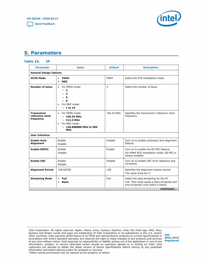
5. ParametersTable 19. IP
Parameter Value Default Description
General Design Options
XCVR Mode • PAM4• NRZ
PAM4 Select the PCS modulation mode.
Number of lanes • For PAM4 mode:— 2— 4— 6— 8
• For NRZ mode:— 1 to 16
2 Select the number of lanes.
Transceiverreference clockfrequency
• For PAM4 mode:— 156.25 MHz— 312.5 MHz
• For NRZ mode:— 138.888888 MHz to 500
MHz
156.25 MHz Specifies the transceiver's reference clockfrequency.
User Interface
Enable AutoAlignment
EnableDisable
Disable Turn on to enable automatic lane alignmentfeature.
Enable RSFEC EnableDisable
Enable Turn on to enable the RS-FEC feature.For PAM4 PCS modulation mode, RS-FEC isalways enabled.
Enable CRC EnableDisable
Disable Turn on to enable CRC error detection andcorrection.
Alignment Period 128-65536 128 Specifies the alignment marker period.The value must be x2.
Streaming Mode • Full• Basic
Full Select the data streaming for the IP.Full: This mode sends a start-of-packet andend-of-packet cycle within a frame.
continued...
UG-20240 | 2020.03.12
Send Feedback
Intel Corporation. All rights reserved. Agilex, Altera, Arria, Cyclone, Enpirion, Intel, the Intel logo, MAX, Nios,Quartus and Stratix words and logos are trademarks of Intel Corporation or its subsidiaries in the U.S. and/orother countries. Intel warrants performance of its FPGA and semiconductor products to current specifications inaccordance with Intel's standard warranty, but reserves the right to make changes to any products and servicesat any time without notice. Intel assumes no responsibility or liability arising out of the application or use of anyinformation, product, or service described herein except as expressly agreed to in writing by Intel. Intelcustomers are advised to obtain the latest version of device specifications before relying on any publishedinformation and before placing orders for products or services.*Other names and brands may be claimed as the property of others.
ISO9001:2015Registered

Parameter Value Default Description
Basic: This is a pure streaming modewhere data is sent without a start-of-packet, empty, and end-of-packet toincrease bandwidth.
Transceiver datarate
• For PAM4 mode:— 32.0 Gbps— 40.0 Gbps— 53.125 Gbps— 56.0 Gbps
• For NRZ with RS-FEC disabledmode:— 9.92 Gbps to 28.0 Gbps
• For NRZ with RS-FEC enabledmode:— 10.3125 Gbps to 28.0 Gbps
53.125 Gbps(PAM4)25.0 Gbps(NRZ)
Specifies the effective data rate at theoutput of the transceiver incorporatingtransmission and other overheads. Thevalue is calculated by the IP by roundingup to 1 decimal place in Gbps unit.
IP Debug and Phy Dynamic Reconfiguration
Table 20. Native Transceiver Phy
Parameter Value Default Description
Dynamic Reconfiguration
Enable dynamicreconfiguration
— Enable Turn on to enable dynamic reconfiguration interface of TransceiverNative PHY.
Enable Native PHY DebugMaster Endpoint
DisableEnable
Disable Turn on to enable the Native PHY Debug Master Endpoint andOptional Reconfiguration Logic Parameters of Transceiver NativePHY.
Optional Reconfiguration Logic
Enable capability registers DisableEnable
Disable Turn on to enable capability register of Transceiver Native PHY,which provide high level information about the transceiver PLLconfiguration.
Set user-defined IP identifier — 0 Sets a user-defined numeric identifier that can be read from theuser-identifier offset when the capability registers are enabled.You must enable the Enable capability registers parameter tochange the value for this parameter.
Enable control and statusregisters
DisableEnable
Disable Turn on to enable control and status registers of Transceiver NativePHY.
For parameters in the PMA Adaptation tab, refer to the PMA Adaptation topic in theE-Tile Transceiver PHY User Guide.
Related Information
• E-Tile Transceiver PHY User Guide: PMA ParametersInformation about PMA Adaptation parameters.
• E-Tile Transceiver PHY User Guide: Dynamic Reconfiguration ExamplesInformation about configuring PMA parameters.
• Serial Lite IV Intel FPGA IP Clock Architecture on page 28
• Clock Signals on page 44
5. Parameters
UG-20240 | 2020.03.12
Send Feedback Serial Lite IV Intel® FPGA IP User Guide
43

6. Serial Lite IV Intel FPGA IP Interface Signals
6.1. Clock Signals
Table 21. Clock Signals
Name Width Direction Description
tx_core_clkout 1 Output TX core clock for the TX custom PCS interface, TX MAC and user logics in the TXdatapath.This clock is generated from the custom PCS block.
rx_core_clkout 1 Output RX core clock for the RX custom PCS interface, RX deskew FIFO, RX MAC and userlogics in the RX datapath.This clock is generated from the custom PCS block.
xcvr_ref_clk 1 Input Transceiver reference clock.The IP supports reference clocks provided from separate clock chips or oscillatorswith a tolerance of ±100 ppm clock variation between the different clock chips oroscillators.Refer to Parameters for supported frequency range.
reconfig_clk 1 Input Input clock for transceiver reconfiguration interface.The clock frequency is 100 to 162 MHz.Connect this input clock signal to external clock circuits or oscillators.
Related Information
Parameters on page 42
6.2. Reset Signals
Table 22. Reset Signals
Name Width Direction Clock Domain Description
tx_core_rst_n 1 Input Asynchronous Active-low reset signal.Resets the Serial Lite IV TX MAC.
rx_core_rst_n 1 Input Asynchronous Active-low reset signal.Resets the Serial Lite IV RX MAC.
tx_pcs_fec_phy_reset_n 1 Input Asynchronous Active-low reset signal.Resets the Serial Lite IV TX custom PCS.
rx_pcs_fec_phy_reset_n 1 Input Asynchronous Active-low reset signal.Resets the Serial Lite IV RX custom PCS.
reconfig_reset • lane/2 (PAM4mode)
• lane/4 (NRZmode)
Input reconfig_clk Active-low reset signal.Resets the Avalon memory-mappedinterface reconfiguration block.
UG-20240 | 2020.03.12
Send Feedback
Intel Corporation. All rights reserved. Agilex, Altera, Arria, Cyclone, Enpirion, Intel, the Intel logo, MAX, Nios,Quartus and Stratix words and logos are trademarks of Intel Corporation or its subsidiaries in the U.S. and/orother countries. Intel warrants performance of its FPGA and semiconductor products to current specifications inaccordance with Intel's standard warranty, but reserves the right to make changes to any products and servicesat any time without notice. Intel assumes no responsibility or liability arising out of the application or use of anyinformation, product, or service described herein except as expressly agreed to in writing by Intel. Intelcustomers are advised to obtain the latest version of device specifications before relying on any publishedinformation and before placing orders for products or services.*Other names and brands may be claimed as the property of others.
ISO9001:2015Registered

6.3. MAC Signals
Table 23. TX MAC SignalsIn this table, N represents the number of lanes set in the IP parameter editor.
Name Width Direction Clock Domain Description
tx_avs_ready 1 Output tx_core_clkout Avalon streaming signal.When asserted, indicates that the TXMAC is ready to accept data.
tx_avs_data • (64*N)*2(PAM4mode)
• 64*N (NRZmode)
Input tx_core_clkout Avalon streaming signal.TX data.
tx_avs_channel 8 Input tx_core_clkout Avalon streaming signal.The channel number for data beingtransferred on the current cycle.This signal is not available in Basic mode.
tx_avs_valid 1 Input tx_core_clkout Avalon streaming signal.When asserted, indicates the TX datasignal is valid.
tx_avs_startofpacket 1 Input tx_core_clkout Avalon streaming signal.When asserted, indicates the start of aTX data packet.Assert for only a single clock cycle foreach packet.This signal is not available in Basic mode.
tx_avs_endofpacket 1 Input tx_core_clkout Avalon streaming signal.When asserted, indicates the end of a TXdata packet.Assert for only a single clock cycle foreach packet.This signal is not available in Basic mode.
tx_avs_empty 5 Input tx_core_clkout Avalon streaming signal.Indicates the number of non-valid wordsin the final burst of the TX data.This signal is not available in Basic mode.
tx_num_valid_bytes_eob 4 Input tx_core_clkout Indicates the number of valid bytes in thelast word of the final burst.This signal is not available in Basic mode.
tx_is_usr_cmd 1 Input tx_core_clkout When asserted, this signal initiate a user-defined information cycle.Assert this signal at the same clock cycleas tx_startofpacket assertion.This signal is not available in Basic mode.
tx_link_up 1 Output tx_core_clkout When asserted, indicates the TX data linkis ready for data transmission.
tx_link_reinit 1 Output tx_core_clkout When asserted, this signal initiates lanesre-alignment.
continued...
6. Serial Lite IV Intel FPGA IP Interface Signals
UG-20240 | 2020.03.12
Send Feedback Serial Lite IV Intel® FPGA IP User Guide
45

Name Width Direction Clock Domain Description
Assert this signal for one clock cycle totrigger the MAC to send ALIGN CW.
crc_error_inject N Input tx_core_clkout When asserted, the MAC injects a CRC32error to selected lanes.
tx_error 5 Output tx_core_clkout Not used.
The following timing diagram shows an example of TX data transmissions of 10 wordsfrom user logic across 10 TX serial lanes.
Figure 28. TX Data Transmission Timing Diagram
............
............
STRT 0 10 N-10
...... ...0,1,2,...,910,11...190,1..,19 N-10.. N-10..
END STRT 0 N-10 END IDLE IDLE
............ STRT 1 11 N-9 END STRT 1 N-9 END IDLE IDLE
............ STRT 9 19 N-1 END STRT 9 N-1 END IDLE IDLE
tx_core_clkout
tx_avs_valid
tx_avs_ready
tx_avs_startofpackets
tx_avs_endofpackets
tx_avs_data
Lane 0
Lane 1
Lane 9
Table 24. RX MAC SignalsIn this table, N represents the number of lanes set in the IP parameter editor.
Name Width Direction Clock Domain Description
rx_avs_ready 1 Input rx_core_clkout Avalon streaming signal.When asserted, indicates that the userlogic is ready to accept data.
rx_avs_data (64*N)*2(PAM4 mode)64*N (NRZ
mode)
Output rx_core_clkout Avalon streaming signal.RX data.
rx_avs_channel 8 Output rx_core_clkout Avalon streaming signal.The channel number for data beingreceived on the current cycle.This signal is not available in Basic mode.
rx_avs_valid 1 Output rx_core_clkout Avalon streaming signal.When asserted, indicates the RX datasignal is valid.
rx_avs_startofpacket 1 Output rx_core_clkout Avalon streaming signal.When asserted, indicates the start of an RXdata packet.Assert for only a single clock cycle for eachpacket.This signal is not available in Basic mode.
rx_avs_endofpacket 1 Output rx_core_clkout Avalon streaming signal.
continued...
6. Serial Lite IV Intel FPGA IP Interface Signals
UG-20240 | 2020.03.12
Serial Lite IV Intel® FPGA IP User Guide Send Feedback
46
Name Width Direction Clock Domain Description
When asserted, indicates the end of an RXdata packet.Assert for only a single clock cycle for eachpacket.This signal is not available in Basic mode.
rx_avs_empty 5 Output rx_core_clkout Avalon streaming signal.Indicates the number of non-valid words inthe final burst of the RX data.This signal is not available in Basic mode.
rx_num_valid_bytes_eob 4 Output rx_core_clkout Indicates the number of valid bytes in thelast word of the final burst.This signal is not available in Basic mode.
rx_is_usr_cmd 1 Output rx_core_clkout When asserted, this signal initiate a user-defined information cycle.Assert this signal at the same clock cycleas tx_startofpacket assertion.This signal is not available in Basic mode.
rx_link_up 1 Output rx_core_clkout When asserted, indicates the RX data linkis ready for data reception.
rx_link_reinit 1 Input rx_core_clkout When asserted, this signal initiates lanesre-alignment.If you disable Enable Auto Alignment,assert this signal for one clock cycle totrigger the MAC to re-align the lanes. If theEnable Auto Alignment is set, the MACre-align the lanes automatically.Do not assert this signal when EnableAuto Alignment is set.
rx_error (N*2*2)+3(PAM4 mode)
(N*2)*3(NRZ mode)
Output rx_core_clkout When asserted, indicates error conditionsoccur in the RX datapath.• [(N*2+2):N+3] = Indicates PCS error
for specific lane.• [N+2] = Indicates alignment error. Re-
initialize lane alignment if this bit isasserted.
• [N+1]= Indicates data is forwarded tothe user logic when user logic is notready.
• [N] = Indicates loss of alignment.• [(N-1):0] = Indicates the data contains
CRC error.
6.4. Transceiver Reconfiguration Signals
Table 25. PCS Reconfiguration SignalsIn this table, N represents the number of lanes set in the IP parameter editor.
Name Width Direction Clock Domain Description
phy_reconfig_read N/2 (PAM4 mode)N (NRZ mode)
Input reconfig_clk PCS reconfiguration read commandsignals.
phy_reconfig_write N/2 (PAM4 mode)N (NRZ mode)
Input reconfig_clk PCS reconfiguration writecommand signals.
continued...
6. Serial Lite IV Intel FPGA IP Interface Signals
UG-20240 | 2020.03.12
Send Feedback Serial Lite IV Intel® FPGA IP User Guide
47

Name Width Direction Clock Domain Description
phy_reconfig_address 21*(N/2) (PAM4mode)
19*N (NRZ mode)
Input reconfig_clk Specifies PCS reconfigurationAvalon memory-mapped interfaceaddress in a selected lane.For NRZ mode, each lane has 19bits and lane 0 address starts fromphy_reconfig_address[18:0].Example, for a 4-lane NRZ design:• phy_reconfig_address[18:
0] = address for lane 0.• phy_reconfig_address[37:
19] = address for lane 1.• phy_reconfig_address[56:
38] = address for lane 2.• phy_reconfig_address[75:
57] = address for lane 3.For PAM4 mode, the lower 19 bitswithin the 21-bit bus specify theaddress and the upper 2 bitsspecify the lane.Example, for a 4-lane PAM4design:• phy_reconfig_address[18:
0] = address for lane 0 and 1,phy_reconfig_address[20:19] = lane number 0 and 1.
• phy_reconfig_address[39:21] = address for lane 2and 3,phy_reconfig_address[41:40] = lane number 2 and 3.
phy_reconfig_readdata 32*(N/2)32*N (NRZ mode)
Output reconfig_clk Specifies PCS reconfiguration datato be read by a ready cycle in aselected lane.
phy_reconfig_waitrequest N/2 (PAM4 mode)N (NRZ mode)
Output reconfig_clk Represents PCS reconfigurationAvalon memory-mapped interfacestalling signal in a selected lane.
phy_reconfig_writedata 32*(N/2) (PAM4mode)
32*N (NRZ mode)
Input reconfig_clk Specifies PCS reconfiguration datato be written on a write cycle in aselected lane.
phy_reconfig_readdata_valid
N/2 (PAM4 mode)N (NRZ mode)
Output reconfig_clk Specifies PCS reconfigurationreceived data is valid in a selectedlane.
Table 26. PMA Reconfiguration SignalsIn this table, N represents the number of lanes set in the IP parameter editor.
Name Width Direction Clock Domain Description
xcvr_reconfig_read N*2 (PAM4 mode)N (NRZ mode)
Input reconfig_clk PMA reconfiguration readcommand signals.
xcvr_reconfig_write N*2 (PAM4 mode)N (NRZ mode)
Input reconfig_clk PMA reconfiguration writecommand signals.
xcvr_reconfig_address 19*N*2 (PAM4mode)
19*N (NRZ mode)
Input reconfig_clk Specifies PMA Avalon memory-mapped interface address in aselected lane.
continued...
6. Serial Lite IV Intel FPGA IP Interface Signals
UG-20240 | 2020.03.12
Serial Lite IV Intel® FPGA IP User Guide Send Feedback
48
Name Width Direction Clock Domain Description
In both PAM4 ad NRZ modes, eachlane has 19 bits and lane 0address starts fromxcvr_reconfig_address[18:0].Example, for a 4-lane design:• xcvr_reconfig_address[18
:0] = address for lane 0.• xcvr_reconfig_address[37
:19] = address for lane 1.• xcvr_reconfig_address[56
:38] = address for lane 2.• xcvr_reconfig_address[75
:57] = address for lane 3.
xcvr_reconfig_readdata 8*N*2 (PAM4mode)
8*N (NRZ mode)
Output reconfig_clk Specifies PMA data to be read by aready cycle in a selected lane.
xcvr_reconfig_waitrequest N*2 (PAM4 mode)N (NRZ mode)
Output reconfig_clk Represents PMA Avalon memory-mapped interface stalling signal ina selected lane.
xcvr_reconfig_writedata 8*N*2 (PAM4mode)
8*N (NRZ mode)
Input reconfig_clk Specifies PMA data to be writtenon a write cycle in a selected lane.
Table 27. RS-FEC Reconfiguration Signals
Name Width Direction Clock Domain Description
rsfec_reconfig_read 1 Input reconfig_clk RS-FEC reconfiguration read command signal.
rsfec_reconfig_write 1 Input reconfig_clk RS-FEC reconfiguration write commandsignal.
rsfec_reconfig_address 11 +lane
offset
Input reconfig_clk Specifies RS-FEC reconfiguration Avalonmemory-mapped interface address.For PAM4 mode:• If N/2 = 1, lane offset is 0• If N/2 = 2, lane offset is 1• If N/2 = 3, lane offset is 2• If N/2 = 4, lane offset is 2For NRZ mode:• For number of lanes from 1 to 4, the lane
offset is 0.• For number of lanes from 5 to 8, the lane
offset is 1.• For number of lanes from 9 to 16, the
lane offset is 2.
rsfec_reconfig_readdata 8 Output reconfig_clk Specifies RS-FEC reconfiguration data to beread by a ready cycle in a selected lane.
rsfec_reconfig_waitrequest 1 Output reconfig_clk Represents RS-FEC reconfiguration Avalonmemory-mapped interface stalling signal in aselected lane.
rsfec_reconfig_writedata 8 Input reconfig_clk Specifies RS-FEC reconfiguration data to bewritten on a write cycle in a selected lane.
6. Serial Lite IV Intel FPGA IP Interface Signals
UG-20240 | 2020.03.12
Send Feedback Serial Lite IV Intel® FPGA IP User Guide
49
6.5. PMA Signals
Table 28. PMA SignalsIn this table, N represents the number of lanes set in the IP parameter editor.
Name Width Direction Clock Domain Description
phy_tx_lanes_stable N*2 (PAM4mode)
N (NRZ mode)
Output Asynchronous When asserted, indicates TX datapath is readyto send data.
tx_pll_locked N*2 (PAM4mode)
N (NRZ mode)
Output Asynchronous When asserted, indicates the TX PLL hasachieved lock status.
phy_ehip_ready N*2 (PAM4mode)
N (NRZ mode)
Output Asynchronous When asserted, indicates that the custom PCShas completed internal initialization and readyfor transmission.This signal asserts aftertx_pcs_fec_phy_reset_n andtx_pcs_fec_phy_reset_nare deasserted.
tx_serial_data N*2 (PAM4mode)
N (NRZ mode)
Output TX serial clock TX serial pins.
rx_serial_data N*2 (PAM4mode)
N (NRZ mode)
Input RX serial clock RX serial pins.
phy_rx_block_lock N*2 (PAM4mode)
N (NRZ mode)
Output Asynchronous When asserted, indicates that the 66b blockalignment has completed for the lanes.
rx_cdr_lock N*2 (PAM4mode)
N (NRZ mode)
Output Asynchronous When asserted, indicates that the recoveredclocks are locked to data.
phy_rx_pcs_ready N*2 (PAM4mode)
N (NRZ mode)
Output Asynchronous When asserted, indicates that the RX lanes ofthe corresponding Ethernet channel are fullyaligned and ready to receive data.
phy_rx_hi_ber N*2 (PAM4mode)
N (NRZ mode)
Output Asynchronous When asserted, indicates that the RX PCS of thecorresponding Ethernet channel is in a HI BERstate.
6. Serial Lite IV Intel FPGA IP Interface Signals
UG-20240 | 2020.03.12
Serial Lite IV Intel® FPGA IP User Guide Send Feedback
50
7. Designing with Serial Lite IV Intel FPGA IP
7.1. Reset Guidelines
Follow these reset guidelines to implement your system-level reset.
• Tie tx_pcs_fec_phy_reset_n and rx_pcs_fec_phy_reset_n signalstogether on the system level in order to reset the TX and RX PCS simultaneously.
• Assert tx_pcs_fec_phy_reset_n, rx_pcs_fec_phy_reset_n,tx_core_rst_n, rx_core_rst_n, and reconfig_reset signals at the sametime. Refer to Reset and Link Initialization for more information about the IP resetand initialization sequences.
• Hold tx_pcs_fec_phy_reset_n, and rx_pcs_fec_phy_reset_n signals low,and reconfig_reset signal high for at least 200 ns to properly reset the customPCS and the reconfiguration blocks.
• To achieve fast link-up between FPGA devices, reset connected Serial Lite IV IntelFPGA IP cores at the same time. Refer to Serial Lite IV Intel Stratix 10 FPGA IPDesign Example User Guide for information about monitoring the IP TX and RX linkusing the toolkit.
Related Information
• Reset and Link Initialization on page 29
• Serial Lite IV Intel Stratix 10 FPGA IP Design Example User Guide: Serial Lite IV IPToolkit
• Serial Lite IV Intel Agilex FPGA IP Design Example User Guide
7.2. Error Handling Guidelines
The following table lists the error handling guidelines for error conditions which mayoccur with the Serial Lite IV Intel FPGA IP design.
UG-20240 | 2020.03.12
Send Feedback
Intel Corporation. All rights reserved. Agilex, Altera, Arria, Cyclone, Enpirion, Intel, the Intel logo, MAX, Nios,Quartus and Stratix words and logos are trademarks of Intel Corporation or its subsidiaries in the U.S. and/orother countries. Intel warrants performance of its FPGA and semiconductor products to current specifications inaccordance with Intel's standard warranty, but reserves the right to make changes to any products and servicesat any time without notice. Intel assumes no responsibility or liability arising out of the application or use of anyinformation, product, or service described herein except as expressly agreed to in writing by Intel. Intelcustomers are advised to obtain the latest version of device specifications before relying on any publishedinformation and before placing orders for products or services.*Other names and brands may be claimed as the property of others.
ISO9001:2015Registered

Table 29. Error Condition and Handling Guidelines
Error Condition Guidelines
One or more lanes cannot establish communication after agiven time frame.
Implement a time-out system to reset the link at theapplication level.
A lane loses communication after communication isestablished.
This may happen after or during the data transfer phases.Implement a link loss detection at the application level andreset the link.
A lane loses communication during the deskew process. Implement link reinitialization process for the erroneouslane.
Loss lane alignment after all lanes have been aligned. This may happen after or during data transfer phases.Implement a lane alignment loss detection at theapplication level to restart the lane alignment process.
7.3. E-Tile Channel Placement Tool
You can use the Intel Stratix 10 E-Tile Channel Placement Tool to plan your channelplacement for Serial Lite IV Intel FPGA IP.
E-tile supports Data Centers, 5G networks, Smart Grid, and other market segments.Ethernet, CPRI, and OTN are the backbone of these emerging and traditionaltechnologies. The E-Tile Channel Placement Tool, in conjunction with the DeviceFamily Pin Connection Guidelines, allows you to swiftly plan protocol placements in theproduct prior to reading comprehensive documentation and implementing designs inIntel Quartus Prime.
The Excel-based E-Tile Channel Placement Tool, supplemented with Instructions,Legend, and Revision tabs, is available for download at E-Tile Channel PlacementTool.
Figure 29. E-Tile Channel Placement Tool
Related Information
• Intel Stratix 10 Device Family Pin Connection Guidelines
• Intel Agilex Device Family Pin Connection Guidelines
7. Designing with Serial Lite IV Intel FPGA IP
UG-20240 | 2020.03.12
Serial Lite IV Intel® FPGA IP User Guide Send Feedback
52

8. Serial Lite IV Intel FPGA IP RegistersThere is no register available for the Serial Lite IV MAC. However, the IP utilizes theRS-FEC and PMA registers in the custom PCS. The following table lists the baseaddresses for the RS-FEC and PMA registers.
Table 30. RS-FEC and PMA Register Base Address
Register Type Address Range
TX and RX RS-FEC registers 0x000-0x2FF
PMA capability registers 0x40000-0x40144
PMA Avalon memory-mapped interface registers 0x000-0x207
For information on RS-FEC and PMA registers, refer to the E-Tile Transceiver PHY UserGuide.
Related Information
• E-Tile Transceiver PHY User Guide: RS-FEC Registers
• E-Tile Transceiver PHY User Guide: PMA Register Map
UG-20240 | 2020.03.12
Send Feedback
Intel Corporation. All rights reserved. Agilex, Altera, Arria, Cyclone, Enpirion, Intel, the Intel logo, MAX, Nios,Quartus and Stratix words and logos are trademarks of Intel Corporation or its subsidiaries in the U.S. and/orother countries. Intel warrants performance of its FPGA and semiconductor products to current specifications inaccordance with Intel's standard warranty, but reserves the right to make changes to any products and servicesat any time without notice. Intel assumes no responsibility or liability arising out of the application or use of anyinformation, product, or service described herein except as expressly agreed to in writing by Intel. Intelcustomers are advised to obtain the latest version of device specifications before relying on any publishedinformation and before placing orders for products or services.*Other names and brands may be claimed as the property of others.
ISO9001:2015Registered

9. Serial Lite IV Intel FPGA IP User Guide ArchivesIP versions are the same as the Intel Quartus Prime Design Suite software versions upto v19.1. From Intel Quartus Prime Design Suite software version 19.2 or later, IPcores have a new IP versioning scheme.
If an IP core version is not listed, the user guide for the previous IP core version applies.
IP Core Version User Guide
1.1.0 Serial Lite IV Streaming Intel FPGA IP User Guide
1.0.0 Serial Lite IV Streaming Intel FPGA IP User Guide
UG-20240 | 2020.03.12
Send Feedback
Intel Corporation. All rights reserved. Agilex, Altera, Arria, Cyclone, Enpirion, Intel, the Intel logo, MAX, Nios,Quartus and Stratix words and logos are trademarks of Intel Corporation or its subsidiaries in the U.S. and/orother countries. Intel warrants performance of its FPGA and semiconductor products to current specifications inaccordance with Intel's standard warranty, but reserves the right to make changes to any products and servicesat any time without notice. Intel assumes no responsibility or liability arising out of the application or use of anyinformation, product, or service described herein except as expressly agreed to in writing by Intel. Intelcustomers are advised to obtain the latest version of device specifications before relying on any publishedinformation and before placing orders for products or services.*Other names and brands may be claimed as the property of others.
ISO9001:2015Registered

10. Document Revision History for the Serial Lite IV IntelFPGA IP User Guide
Document Version Intel QuartusPrime Version
Intel FPGA IPVersion
Changes
2020.03.12 19.4 1.2.0 • Updated effective rates for PAM4 transceiver modein the Bandwidth Efficiency table.
• Removed the effective rate calculation for PAM4 inthe Link Rate and Bandwidth Efficiency Calculationtopic.
• Added PMA Adaptation Flow topic and link to theEthernet Adaptation Flow with Non-external AIBClocking in the E-tile Hard IP User Guide: E-TileHard IP for Ethernet and E-Tile CPRI PHY Intel FPGAIPs user guide.
2020.01.23 19.4 1.2.0 • Added ALM count and IP latency for NRZ with RS-FEC enabled mode in the Intel Stratix 10 Serial LiteIV Intel FPGA IP Resource Utilization and IntelAgilex Serial Lite IV Intel FPGA IP ResourceUtilization tables.
• Added bandwidth efficiency values for NRZ with RS-FEC enabled mode in the Bandwidth Efficiencytable.
• Updated the effective rate calculations for both NRZand PAM4 features in the Link Rate and BandwidthEfficiency Calculation topic.
• Updated values for the following parameters in theParameters topic:— Transceiver data rate— Set user-defined IP identifier
• Updated rsfec_reconfig_address signalsdescription for NRZ mode.
• Added description to decode addresses and lanenumbers for the phy_reconfig_address andxcvr_reconfig_address signals.
2019.09.30 19.3 1.1.0 • Changed IP name to Serial Lite IV Intel FPGA IP.• Added support for Intel Agilex devices.• Added support for NRZ mode.• Added information for CRC feature.• Updated PCS, PMA and RS-FEC reconfiguration
signals width.
2019.07.01 19.2 1.0.0 Initial release.
UG-20240 | 2020.03.12
Send Feedback
Intel Corporation. All rights reserved. Agilex, Altera, Arria, Cyclone, Enpirion, Intel, the Intel logo, MAX, Nios,Quartus and Stratix words and logos are trademarks of Intel Corporation or its subsidiaries in the U.S. and/orother countries. Intel warrants performance of its FPGA and semiconductor products to current specifications inaccordance with Intel's standard warranty, but reserves the right to make changes to any products and servicesat any time without notice. Intel assumes no responsibility or liability arising out of the application or use of anyinformation, product, or service described herein except as expressly agreed to in writing by Intel. Intelcustomers are advised to obtain the latest version of device specifications before relying on any publishedinformation and before placing orders for products or services.*Other names and brands may be claimed as the property of others.
ISO9001:2015Registered