serial-in / parallel-out driver series serial / parallel 4 ... filepower dissipation 1 pd1 450 *1...
TRANSCRIPT
1/24 www.rohm.com 2009.06 - Rev.A
© 2009 ROHM Co., Ltd. All rights reserved.
Serial-in / Parallel-out Driver Series
Serial / Parallel 4-input Drivers
BU2050F,BU2092F,BU2092FV,BU2099FV,BD7851FP,BU2152FS Description
Serial-in-parallel-out driver incorporates a built-in shift register and a latch circuit to control a maximum of 24 LED by a 4-line interface, linked to a microcontroller. A single external resistor can set the output current value of the constant current up to a maximum of 50mA. (BD7851FP only) CMOS open drain output type products can drive the maximum current of 25mA.
Features 1) LED can be driven directly. 2) Parallel output of a maximum of 24 bit 3) Operational on low voltage (2.7V to 5.5V) 4) Cascade connection is possible (BU2050F and BU2092F,BU2092FV are not acceptable)
Application
For AV equipment such as, audio stereo sets, videos and TV sets, PCs, control microcontroller mounted equipment. Product line-up
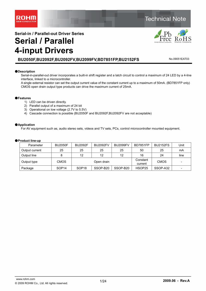
Parameter BU2050F BU2092F BU2092FV BU2099FV BD7851FP BU2152FS Unit
Output current 25 25 25 25 50 25 mA
Output line 8 12 12 12 16 24 line
Output type CMOS Open drain Constant current
CMOS -
Package SOP14 SOP18 SSOP-B20 SSOP-B20 HSOP25 SSOP-A32 -
No.09051EAT03
BU2050F,BU2092F,BU2092FV,BU2099FV,BD7851FP,BU2152FS Technical Note
2/24 www.rohm.com 2009.06 - Rev.A
© 2009 ROHM Co., Ltd. All rights reserved.
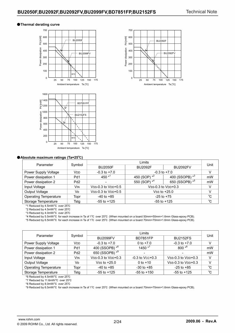
Thermal derating curve
Absolute maximum ratings (Ta=25)
Parameter Symbol Limits
Unit BU2050F BU2092F BU2092FV
Power Supply Voltage VDD -0.3 to +7.0 -0.3 to +7.0 V Power dissipation 1 Pd1 450 *1 450 (SOP) *2 400 (SSOPB) *3 mW Power dissipation 2 Pd2 - 550 (SOP) *4 650 (SSOPB) *5 mW Input Voltage VIN VSS-0.3 to VDD+0.5 VSS-0.3 to VDD+0.3 V Output Voltage Vo VSS-0.3 to VDD+0.5 VSS to +25.0 V Operating Temperature Topr -40 to +85 -25 to +75 Storage Temperature Tstg -55 to +125 -55 to +125 *1 Reduced by 4.5mW/ over 25 *2 Reduced by 4.5mW/ over 25 *3 Reduced by 4.0mW/ over 25 *4 Reduced by 5.5mW/ for each increase in Ta of 1 over 25 (When mounted on a board 50mm×50mm×1.6mm Glass-epoxy PCB). *5 Reduced by 6.5mW/ for each increase in Ta of 1 over 25 (When mounted on a board 70mm×70mm×1.6mm Glass-epoxy PCB).
Parameter Symbol Limits
Unit BU2099FV BD7851FP BU2152FS
Power Supply Voltage VDD -0.3 to +7.0 0 to +7.0 -0.3 to +7.0 V Power dissipation 1 Pd1 400 (SSOPB) *6 1450 *7 800 *8 mW Power dissipation 2 Pd2 650 (SSOPB) *9 - - mW Input Voltage VIN VSS-0.3 to VDD+0.3 -0.3 to VCC+0.3 VSS-0.3 to VDD+0.3 V Output Voltage Vo VSS to +25.0 0 to +10 VSS-0.3 to VDD+0.3 V Operating Temperature Topr -40 to +85 -30 to +85 -25 to +85 Storage Temperature Tstg -55 to +125 -55 to +150 -55 to +125 *6 Reduced by 4.5mW/ over 25 *7 Reduced by 11.6mW/ over 25 *8 Reduced by 8.0mW/ over 25 *9 Reduced by 6.5mW/ for each increase in Ta of 1 over 25 (When mounted on a board 70mm×70mm×1.6mm Glass-epoxy PCB).
700
600
500
400
300
200
100
025 50 75 100 125 150 175
Ambient temperature Ta []
Pow
er d
issi
patio
n
Pd
[mW
]
BU2099FV
85
BU2050F
25 50 75 100 125 150 175
Ambient temperature Ta []
Pow
er d
issi
patio
n
Pd
[mW
]
85
400
200
0
800
600
1200
1000
1600
1400
BU2152FS
BD7851FP
700
600
500
400
300
200
100
025 50 75 100 125 150 175
Ambient temperature Ta []
Pow
er d
issi
patio
n
Pd
[mW
]
BU2092FV
BU2092F

BU2050F,BU2092F,BU2092FV,BU2099FV,BD7851FP,BU2152FS Technical Note
3/24 www.rohm.com 2009.06 - Rev.A
© 2009 ROHM Co., Ltd. All rights reserved.
Electrical characteristics BU2050F (Unless otherwise noted, Ta=25, VDD=4.5 to 5.5V)
Parameter Symbol Min. Typ. Max. Unit Condition
Power Supply Voltage VDD 4.5 - 5.5 V
Input high-level Voltage VIH 0.7VDD - VDD V
Input low-level Voltage VIL VSS - 0.3VDD V
Input Hysteresis VHYS - 0.5 - V
Output high-level Voltage VOHD
VDD-1.5 - VDD
V
IOH=-25mA
VDD-1.0 - VDD IOH=-15mA
VDD-0.5 - VDD IOH=-10mA
Output low-level Voltage VOLD
VSS - 1.5
V
IOL=25mA
VSS - 0.8 IOL=15mA
VSS - 0.4 IOL=10mA
Quiescent Current IDD - - 0.1 mA VIH=VDD, VIL=VSS
BU2092F/BU2092FV (Unless otherwise noted, Ta=25, VSS=0V, VDD=5.0V/3.0V) Parameter Symbol Min. Typ. Max. Unit Condition
Power Supply Voltage VDD 2.7 - 5.5 V
Input high-level Voltage VIH 3.5 / 2.5 - - V VDD=5V/3V
Input low-level Voltage VIL - - 1.5 / 0.4 V VDD=5V/3V
Output low-level Voltage VOL - - 2.0 / 1.0 V VDD=5V/3V, IOL=20mA/5mA
Output high-level disable Current IOZH - - 10.0 μA VO=25.0V
Output low-level disable Current IOZL - - -5.0 μA VO=0V
Quiescent Current IDD - - 5.0 / 3.0 μA VIN=VSS or VDD
(VDD=5V/3V) OUTPUT:OPEN
BU2099FV (Unless otherwise noted, Ta=25, VSS=0V, VDD=5.0V/3.0V)
Parameter Symbol Min. Typ. Max. Unit Condition
Power Supply Voltage VDD 2.7 - 5.5 V
Input high-level Voltage VIH 3.5 / 2.1 - - V VDD=5V/3V
Input low-level Voltage VIL - - 1.5 / 0.9 V VDD=5V/3V
Output high-level Voltage (SO) VOH VDD-0.5
/ VDD-0.3- - V
VDD=5V/3V, IOH=-400μA/-100μA
Output low-level Voltage 1 (Qx) VOL1
- - 1.0
V
VDD=5V/3V, IOL1=10mA/5mA
- - 1.5 VDD=5V, IOL1=15mA
- - 2.0 VDD=5V, IOL1=20mA
Output low-level Voltage 2 (SO) VOL2 - - 0.4 / 0.3 V VDD=5V/3V, IOL2=1.5mA/0.5mA
Output high-level disable Current (Qx)
IOZH - - 10 μA VO=25.0V
Output low-level disable Current (Qx)
IOZL - - -5.0 μA VO=0V
IPULLDOWN (OE) IPD - - 150 / 60 μA OE= VDD, VDD=5V/3V
Low Voltage Reset VCLR 1.1 - 2.4 V
Quiescent Current IDD - - 200 μA VIN=VSS or VDD, VDD=5V
OUTPUT:OPEN
BU2050F,BU2092F,BU2092FV,BU2099FV,BD7851FP,BU2152FS Technical Note
4/24 www.rohm.com 2009.06 - Rev.A
© 2009 ROHM Co., Ltd. All rights reserved.
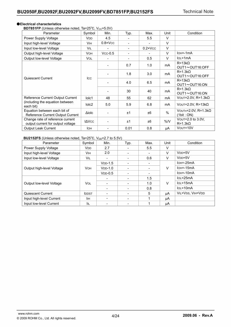
Electrical characteristics BD7851FP (Unless otherwise noted, Ta=25, VCC=5.0V)
Parameter Symbol Min. Typ. Max. Unit Condition
Power Supply Voltage VDD 4.5 - 5.5 V
Input high-level Voltage VIH 0.8×VCC - - V
Input low-level Voltage VIL - - 0.2×VCC V
Output high-level Voltage VOH VCC-0.5 - - V IOH=-1mA
Output low-level Voltage VOL - - 0.5 V IOL=1mA
Quiescent Current ICC
- 0.7 1.0 mA R=13kΩ OUT1~OUT16:OFF
- 1.8 3.0 mA R=1.3kΩ OUT1~OUT16:OFF
- 4.0 6.5 mA R=13kΩ OUT1~OUT16:ON
- 30 40 mA R=1.3kΩ OUT1~OUT16:ON
Reference Current Output Current (including the equation between each bit)
Iolc1 48 55 62 mA VOUT=2.0V, R=1.3kΩ
Iolc2 5.0 5.9 6.8 mA VOUT=2.0V, R=13kΩ
Equation between each bit of Reference Current Output Current
Δiolc - ±1 ±6 % VOUTn=2.0V, R=1.3kΩ(1bit : ON)
Change rate of reference current output current for output voltage
IΔVCC - ±1 ±6 %/V VOUT=2.0 to 3.0V, R=1.3kΩ
Output Leak Current IOH - 0.01 0.8 μA VOUT=10V
BU2152FS (Unless otherwise noted, Ta=25, VDD=2.7 to 5.5V)
Parameter Symbol Min. Typ. Max. Unit Condition
Power Supply Voltage VDD 2.7 - 5.5 V
Input high-level Voltage VIH 2.0 - - V VDD=5V
Input low-level Voltage VIL - - 0.6 V VDD=5V
Output high-level Voltage VOH
VDD-1.5 - -
V
IOH=-25mA
VDD-1.0 - - IOH=-15mA
VDD-0.5 - - IOH=-10mA
Output low-level Voltage VOL
- - 1.5
V
IOL=25mA
- - 1.0 IOL=15mA
- - 0.8 IOL=10mA
Quiescent Current IDDST - - 5 μA VIL=VSS, VIH=VDD
Input high-level Current IIH - - 1 μA
Input low-level Current IIL - - 1 μA

BU2050F,BU2092F,BU2092FV,BU2099FV,BD7851FP,BU2152FS Technical Note
5/24 www.rohm.com 2009.06 - Rev.A
© 2009 ROHM Co., Ltd. All rights reserved.
Block diagram BU2050F
BU2092F/BU2092FV
BU2099FV
BD7851FP
BU2152FS
Controller
Shift
Register
STB
CLR
CLOCK
DATA
8bit
Lat ch
Write
Buffer P1~P8
Controller
Shift
Register
LCK
CLOCK
DATA
12bit
Lat ch
Write
Buffer Q0~Q11
OE
Controller
Shift
Register
LCK
CLOCK
DATA
12bit
Lat ch
Write
Buffer Q0~Q11
OE
LPF
Shift
Register
S_IN16bit
Lat ch
Write
Buffer OUT1~OUT16
LATCH
CLOCK
Controller
Shift
Register
STB
CLB
CLOCK
DATA
24bit
Lat ch
Write
Buffer P1~P24
SO
ENABLE
R_Iref
SOUT
Current Adjustment
BU2050F,BU2092F,BU2092FV,BU2099FV,BD7851FP,BU2152FS Technical Note
6/24 www.rohm.com 2009.06 - Rev.A
© 2009 ROHM Co., Ltd. All rights reserved.
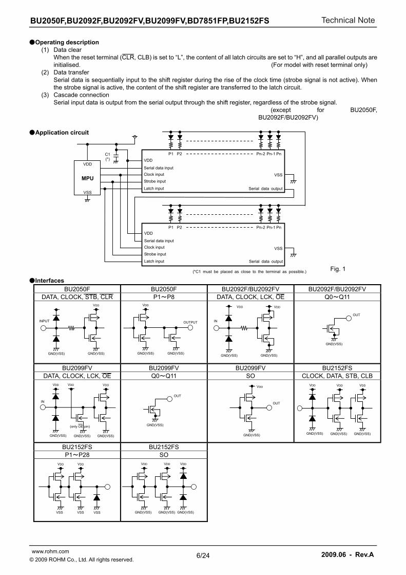
Operating description (1) Data clear
When the reset terminal (CLR, CLB) is set to “L”, the content of all latch circuits are set to “H”, and all parallel outputs are initialised. (For model with reset terminal only)
(2) Data transfer Serial data is sequentially input to the shift register during the rise of the clock time (strobe signal is not active). When the strobe signal is active, the content of the shift register are transferred to the latch circuit.
(3) Cascade connection Serial input data is output from the serial output through the shift register, regardless of the strobe signal.
(except for BU2050F, BU2092F/BU2092FV)
Application circuit
Fig. 1
Interfaces BU2050F BU2050F BU2092F/BU2092FV BU2092F/BU2092FV
DATA, CLOCK, STB, CLR P1~P8 DATA, CLOCK, LCK, OE Q0~Q11
BU2099FV BU2099FV BU2099FV BU2152FS DATA, CLOCK, LCK, OE Q0~Q11 SO CLOCK, DATA, STB, CLB
BU2152FS BU2152FS P1~P28 SO
VDD
Serial data input
Clock input
Strobe input
Latch input
P1 P2 Pn-2 Pn-1 Pn
Serial data output
VSS
P1 P2 Pn-2 Pn-1 Pn
VSS
VDD
VSS
MPU
C1 (*)
(*C1 must be placed as close to the terminal as possible.)
VDD
Serial data input
Clock input
Strobe input
Latch input Serial data output
INPUT
GND(VSS) GND(VSS)
VDD
GND(VSS)
VDD
OUTPUT
GND(VSS)
IN
GND(VSS) GND(VSS)
VDDVDD
OUT
GND(VSS)
GND(VSS)
VDD
OUT
OUT
GND(VSS)
VSS
VDD VDD
VSS VSS GND(VSS)
VDD VDD VDD
GND(VSS) GND(VSS)
GND(VSS)
VDD VDD
GND(VSS)
VDD
GND(VSS) GND(VSS)
VDD
GND(VSS)
VDD
GND(VSS)
VDD
IN
(only OE pin)
BU2050F,BU2092F,BU2092FV,BU2099FV,BD7851FP,BU2152FS Technical Note
7/24 www.rohm.com 2009.06 - Rev.A
© 2009 ROHM Co., Ltd. All rights reserved.
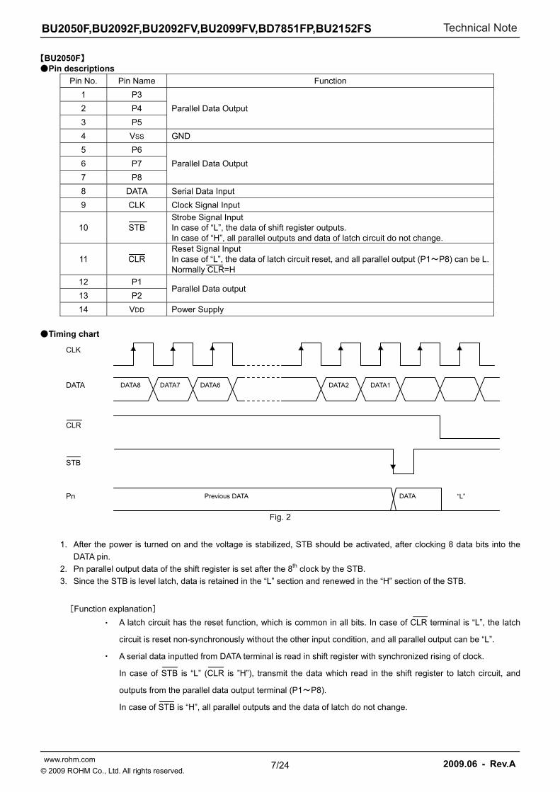
【BU2050F】 Pin descriptions
Pin No. Pin Name Function
1 P3
Parallel Data Output 2 P4
3 P5
4 VSS GND
5 P6
Parallel Data Output 6 P7
7 P8
8 DATA Serial Data Input
9 CLK Clock Signal Input
10 STB Strobe Signal Input In case of “L”, the data of shift register outputs. In case of “H”, all parallel outputs and data of latch circuit do not change.
11 CLR Reset Signal Input In case of “L”, the data of latch circuit reset, and all parallel output (P1~P8) can be L.Normally CLR=H
12 P1 Parallel Data output
13 P2
14 VDD Power Supply
Timing chart
Fig. 2
1. After the power is turned on and the voltage is stabilized, STB should be activated, after clocking 8 data bits into the
DATA pin.
2. Pn parallel output data of the shift register is set after the 8th clock by the STB.
3. Since the STB is level latch, data is retained in the “L” section and renewed in the “H” section of the STB.
[Function explanation]
・ A latch circuit has the reset function, which is common in all bits. In case of CLR terminal is “L”, the latch
circuit is reset non-synchronously without the other input condition, and all parallel output can be “L”.
・ A serial data inputted from DATA terminal is read in shift register with synchronized rising of clock.
In case of STB is “L” (CLR is ”H”), transmit the data which read in the shift register to latch circuit, and
outputs from the parallel data output terminal (P1~P8).
In case of STB is “H”, all parallel outputs and the data of latch do not change.
CLK
STB
DATA DATA8 DATA7 DATA6 DATA2 DATA1
Pn Previous DATA DATA
CLR
“L”

BU2050F,BU2092F,BU2092FV,BU2099FV,BD7851FP,BU2152FS Technical Note
8/24 www.rohm.com 2009.06 - Rev.A
© 2009 ROHM Co., Ltd. All rights reserved.
Switching characteristics (Unless otherwise specified, VDD=4.5 to 5.5V, Ta=25)
Parameter Symbol Limit
Unit Condition Min. Typ. Max.
Set up time (DATA-CLK) tSD 20 - - ns -
Hold time (DATA-CLK) tHD 20 - - ns -
Set up time CLK)STB( tSSTB 30 - - ns -
Hold time CLK)STB( tHSTB 30 - - ns -
Propagation P8)P1CLR( ~ tPDPCK - - 100 ns P1~P8 terminal load 20pF or less
Propagation P8)P1STB( ~ tPDPSTB - - 80 ns P1~P8 terminal load 20pF or less
Propagation P8)P1CLR( ~ tPDPCLR - - 80 ns P1~P8 terminal load 20pF or less
Maximum clock frequency fMAX 5 - - MHz -
Switching Time Test Waveform
Fig. 3
CLK
DATA
P8
P1
STB
CLR
1 2 8 9 10 11 12
fMAX
tHD
tSD
tHSTB tSSTB
tPDPSTB tPDPCLR
tPDPCK

BU2050F,BU2092F,BU2092FV,BU2099FV,BD7851FP,BU2152FS Technical Note
9/24 www.rohm.com 2009.06 - Rev.A
© 2009 ROHM Co., Ltd. All rights reserved.
【BU2092F/BU2092FV】 Pin descriptions
Timing chart
Fig. 4
1. After the power is turned on and the voltage is stabilized, LCK should be activated, after clocking 12 data bits into
the DATA terminal.
2. Qx parallel output data of the shift register is set after the 12th clock by the LCK.
3. Since the LCK is a label latch, data is retained in the “L” section and renewed in the “H” section of the LCK.
4. Data retained in the internal latch circuit is output when the OE is in the “L” section.
[Truth Table]
Input Function
CLOCK DATA LCK OE
× × × H Output (Q0~Q11) Disable
× × × L Output (Q0~Q11) Enable
L × ×
Store “L” in the first stage data of shift register, the previous stage data in the
others. (The conditions of storage register and output have no change.)
H × ×
Store “H” in the first stage data of shift register, the previous stage data in the
others. (The conditions of storage register and output have no change.)
× × × The data of shift register has no change.
× × × The data of shift register is transferred to the storage register.
× × × The data of storage register has no change.
Pin No. Pin Name I/O Function
1 VSS - GND
2 DATA I Serial Data Input
3 CLOCK I Shift clock of DATA (Rising Edge Trigger)
4 LCK I Latch clock of DATA (Rising Edge Trigger)
5~11,
14~18 Q0~Q11 O
Parallel Data Output (Nch Open Drain FET)
Latch Data L H
Output FET ON OFF
12, 13 N.C. - Non connected
17 OE I Output Enable (“H” level : output FET is OFF)
18 VDD - Power Supply
CLOCK
LCK
DATA DATA11 DATA10 DATA9 DATA1 DATA0
OE
Qx Previous DATA DATA11~0 “H”
Note) Diagram shows a status where a pull-up resistor is connected to output.
BU2050F,BU2092F,BU2092FV,BU2099FV,BD7851FP,BU2152FS Technical Note
10/24 www.rohm.com 2009.06 - Rev.A
© 2009 ROHM Co., Ltd. All rights reserved.
Switching characteristics (Unless otherwise specified, VDD=5V, VSS=0V, Ta=25)
Parameter Symbol Limit
Unit
Condition Min. Typ. Max. VDD(V)
Minimum Clock Pulse Width tw 1000 - - ns 3
- 500 - - ns 5
Minimum Latch Pulse Width
(LCK)
tw
(LCK)
1000 - - ns 3 -
500 - - ns 5
Setup Time
(LCK→CLOCK) ts
400 - - ns 3 -
200 - - ns 5
Setup Time
(DATA→CLOCK) tsu
400 - - ns 3 -
200 - - ns 5
Hold Time
(CLOCK→DATA) tH
400 - - ns 3 -
200 - - ns 5
Propagation
(LCK→OUTPUT QX)
tPLZ
(LCK)
- 90 - ns 3 RL=5kΩ
CL=10pF - 55 - ns 5
tPZL (LCK)
- 115 - ns 3 RL=5kΩ
CL=10pF - 50 - ns 5
Propagation
( OE →OUTPUT QX)
tPLZ - 70 - ns 3 RL=5kΩ
CL=10pF - 45 - ns 5
tPZL - 80 - ns 3 RL=5kΩ
CL=10pF - 35 - ns 5
Switching Time Test Circuit
Fig. 5
CLOCK
Pulse Gen.
DATA
Pulse Gen.
Q11
RL
±25V
Q0
RL
±25VVDD
GND (Vss)
Pulse Gen.
Pulse Gen.
LCK
OE
GND (Vss)
GND (Vss)
CL
CL

BU2050F,BU2092F,BU2092FV,BU2099FV,BD7851FP,BU2152FS Technical Note
11/24 www.rohm.com 2009.06 - Rev.A
© 2009 ROHM Co., Ltd. All rights reserved.
【BU2092F/BU2092FV】 Switching Time Test Waveforms
Fig. 6
CLOCK
DATA
tSU
90%
10%
90% 90%
tH
90% 90%
10%
90%
10%
tW tW
50% LCK
50%
90%
10%
tS
90%
tW(CLK)
50% 50%OE
Qx
tPLZ(LCK) tPZL(LCK)
10%
50%10%
tPLZ
50%
tPZL
VDD
GND (VSS)
VDD
GND (VSS)
VDD
GND (VSS)
VDD
GND (VSS)
VDD
GND (VSS)
BU2050F,BU2092F,BU2092FV,BU2099FV,BD7851FP,BU2152FS Technical Note
12/24 www.rohm.com 2009.06 - Rev.A
© 2009 ROHM Co., Ltd. All rights reserved.
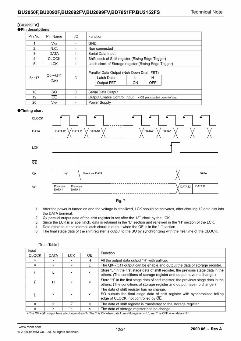
【BU2099FV】 Pin descriptions
Pin No. Pin Name I/O Function
1 VSS - GND 2 N.C. - Non connected 3 DATA I Serial Data Input 4 CLOCK I Shift clock of Shift register (Rising Edge Trigger) 5 LCK I Latch clock of Storage register (Rising Edge Trigger)
6~17 Q0~Q11
(Qx) O
Parallel Data Output (Nch Open Drain FET) Latch Data L H Output FET ON OFF
18 SO O Serial Data Output 19 OE I Output Enable Control Input *OE pin is pulled down to Vss.
20 VDD - Power Supply
Timing chart
Fig. 7
1. After the power is turned on and the voltage is stabilized, LCK should be activates, after clocking 12 data bits into the DATA terminal.
2. Qx parallel output data of the shift register is set after the 12th clock by the LCK. 3. Since the LCK is a label latch, data is retained in the “L” section and renewed in the “H” section of the LCK. 4. Data retained in the internal latch circuit is output when the OE is in the “L” section. 5. The final stage data of the shift register is output to the SO by synchronizing with the rise time of the CLOCK.
[Truth Table]
Input Function
CLOCK DATA LCK OE × × × H All the output data output “H” with pull-up. × × × L The Q0~Q11 output can be enable and output the data of storage register.
L × × Store “L” in the first stage data of shift register, the previous stage data in the others. (The conditions of storage register and output have no change.)
H × ×
Store “H” in the first stage data of shift register, the previous stage data in the others. (The conditions of storage register and output have no change.)
× × ×
The data of shift register has no change. SO outputs the final stage data of shift register with synchronized falling edge of CLOCK, not controlled by OE.
× × × The data of shift register is transferred to the storage register. × × × The data of storage register has no change.
*The Q0~Q11 output have a Nch open drain Tr. The Tr is ON when data from shift register is “L”, and Tr is OFF when data is “H”.
CLOCK
LCK
DATA DATA12 DATA11 DATA10 DATA2 DATA1
OE
Qx Previous DATA DATA
SO Previous DATA 11
Previous DATA 11
DATA12 DATA11
“H”

BU2050F,BU2092F,BU2092FV,BU2099FV,BD7851FP,BU2152FS Technical Note
13/24 www.rohm.com 2009.06 - Rev.A
© 2009 ROHM Co., Ltd. All rights reserved.
【BU2099FV】 Switching characteristics (Unless otherwise specified, VDD=5V, VSS=0V, Ta=25)
Parameter Symbol Limit
Unit
Condition Min. Typ. Max. VDD(V)
Minimum Clock Pulse Width (CLOCK)
tW 1000 - - ns 3
- 500 - - ns 5
Minimum Latch Pulse Width (LCK)
tW (LCK)
1000 - - ns 3 -
500 - - ns 5 Setup Time (LCK→CLOCK)
tS 400 - - ns 3
- 200 - - ns 5
Setup Time (DATA→CLOCK)
tsu 400 - - ns 3
- 200 - - ns 5
Hole Time (CLOCK→DATA)
tH 400 - - ns 3
- 200 - - ns 5
Propagation (SO)
tPLH tPHL
- - 500 ns 3 - - - 250 ns 5 -
Propagation (LCK→QX) *
tPLZ (LCK)
- 360 - ns 3 RL=5kΩ CL=10pF - 170 - ns 5
tPZL
(LCK) - 260 - ns 3 RL=5kΩ
CL=10pF - 175 - ns 5
Propagation ( QE →QX) *
tPLZ - 115 - ns 3 RL=5kΩ
CL=10pF - 85 - ns 5
tPZL - 175 - ns 3 RL=5kΩ
CL=10pF - 65 - ns 5 Noise Pulse Suppression Time (LCK) *
tI - 30 ns -
- - 20 ns -
*Reference value
Input Voltage Test Circuit
Fig. 8 Switching Time Test Circuit
Fig. 9
RL =10kΩ
GND (Vss)
P.G.
VIH
VIL
GND
RL =5kΩ
VDD
GND (Vss)
P.G.
GND(Vss)
CL =10pF
+25V
RL =5kΩ
GND(Vss)
CL =10pF
+25V
BU2050F,BU2092F,BU2092FV,BU2099FV,BD7851FP,BU2152FS Technical Note
14/24 www.rohm.com 2009.06 - Rev.A
© 2009 ROHM Co., Ltd. All rights reserved.
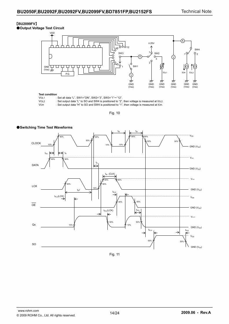
【BU2099FV】 Output Voltage Test Circuit
Fig. 10
Switching Time Test Waveforms
Fig. 11
VDD
GND (Vss)
P.G.
GND(Vss)
GND(Vss)
GND (Vss)
GND (Vss)
GND (Vss)
GND(Vss)
IOL2IOH
SW4
1 2
±25V
SW21
2
3
SW11
12
SW3
Test condition VOL1 :Set all data “L”. SW1=”ON”, SW2=”3”, SW3=”1”~”12”. VOL2 :Set output data “L” to SO and SW4 is positioned to “2”, then voltage is measured at IOL2. VOH :Set output data “H” to SO and SW4 is positioned to “1”, then voltage is measured at IOH.
CLOCK
DATA
tSU
90%
10%
90% 90%
tH
90% 90%
10%
90%
10%
tW tW
50%LCK
50%
90%
10%
tS
90%
tW (CLK)
50% 50%
OE
Qx
tPLZ
tPZL(LCK)
10%
50%
10%
50%
tPZL
VDD
GND (VSS)
VDD
GND (VSS)
VDD
GND (VSS)
VDD
GND (VSS)
VEXT
GND (VSS)
50% 50% 50%
tS2
tPLZ(LCK)
SO 50% 50%
tPLH tPHL
VDD
GND (VSS)
IOL1
BU2050F,BU2092F,BU2092FV,BU2099FV,BD7851FP,BU2152FS Technical Note
15/24 www.rohm.com 2009.06 - Rev.A
© 2009 ROHM Co., Ltd. All rights reserved.
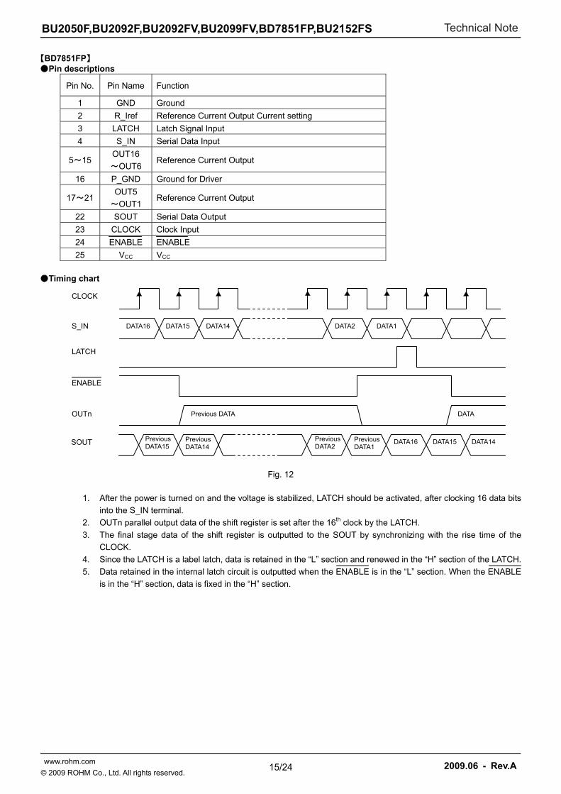
【BD7851FP】 Pin descriptions
Pin No. Pin Name Function
1 GND Ground
2 R_Iref Reference Current Output Current setting
3 LATCH Latch Signal Input
4 S_IN Serial Data Input
5~15 OUT16
~OUT6 Reference Current Output
16 P_GND Ground for Driver
17~21 OUT5
~OUT1 Reference Current Output
22 SOUT Serial Data Output
23 CLOCK Clock Input
24 ENABLE ENABLE
25 VCC VCC
Timing chart
Fig. 12
1. After the power is turned on and the voltage is stabilized, LATCH should be activated, after clocking 16 data bits
into the S_IN terminal.
2. OUTn parallel output data of the shift register is set after the 16th clock by the LATCH.
3. The final stage data of the shift register is outputted to the SOUT by synchronizing with the rise time of the
CLOCK.
4. Since the LATCH is a label latch, data is retained in the “L” section and renewed in the “H” section of the LATCH.
5. Data retained in the internal latch circuit is outputted when the ENABLE is in the “L” section. When the ENABLE
is in the “H” section, data is fixed in the “H” section.
CLOCK
LATCH
S_IN DATA16 DATA15 DATA14 DATA2 DATA1
OUTn Previous DATA DATA
SOUT Previous DATA15
Previous DATA14
Previous DATA2
DATA16 Previous DATA1
DATA15 DATA14
ENABLE
BU2050F,BU2092F,BU2092FV,BU2099FV,BD7851FP,BU2152FS Technical Note
16/24 www.rohm.com 2009.06 - Rev.A
© 2009 ROHM Co., Ltd. All rights reserved.
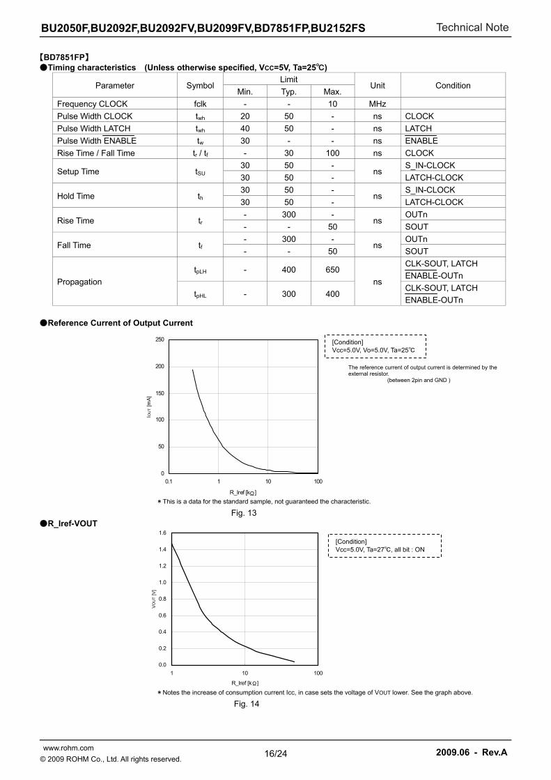
【BD7851FP】 Timing characteristics (Unless otherwise specified, VCC=5V, Ta=25)
Parameter Symbol Limit
Unit Condition Min. Typ. Max.
Frequency CLOCK fclk - - 10 MHz
Pulse Width CLOCK twh 20 50 - ns CLOCK
Pulse Width LATCH twh 40 50 - ns LATCH
Pulse Width ENABLE tw 30 - - ns ENABLE
Rise Time / Fall Time tr / tf - 30 100 ns CLOCK
Setup Time tSU 30 50 -
ns S_IN-CLOCK
30 50 - LATCH-CLOCK
Hold Time th 30 50 -
ns S_IN-CLOCK
30 50 - LATCH-CLOCK
Rise Time tr - 300 -
ns OUTn
- - 50 SOUT
Fall Time tf - 300 -
ns OUTn
- - 50 SOUT
Propagation
tpLH - 400 650
ns
CLK-SOUT, LATCH
ENABLE-OUTn
tpHL - 300 400 CLK-SOUT, LATCH
ENABLE-OUTn
Reference Current of Output Current
*This is a data for the standard sample, not guaranteed the characteristic.
Fig. 13 R_Iref-VOUT
*Notes the increase of consumption current Icc, in case sets the voltage of VOUT lower. See the graph above.
Fig. 14
0
50
100
150
200
250
0.1 1 10 100
R_Iref [kΩ]
IOU
T [
mA
]
[Condition] Vcc=5.0V, Vo=5.0V, Ta=25
0.0
0.2
0.4
0.6
0.8
1.0
1.2
1.4
1.6
1 10 100
R_Iref [kΩ]
VO
UT [V
]
[Condition] Vcc=5.0V, Ta=27, all bit : ON
The reference current of output current is determined by theexternal resistor. (between 2pin and GND )
BU2050F,BU2092F,BU2092FV,BU2099FV,BD7851FP,BU2152FS Technical Note
17/24 www.rohm.com 2009.06 - Rev.A
© 2009 ROHM Co., Ltd. All rights reserved.
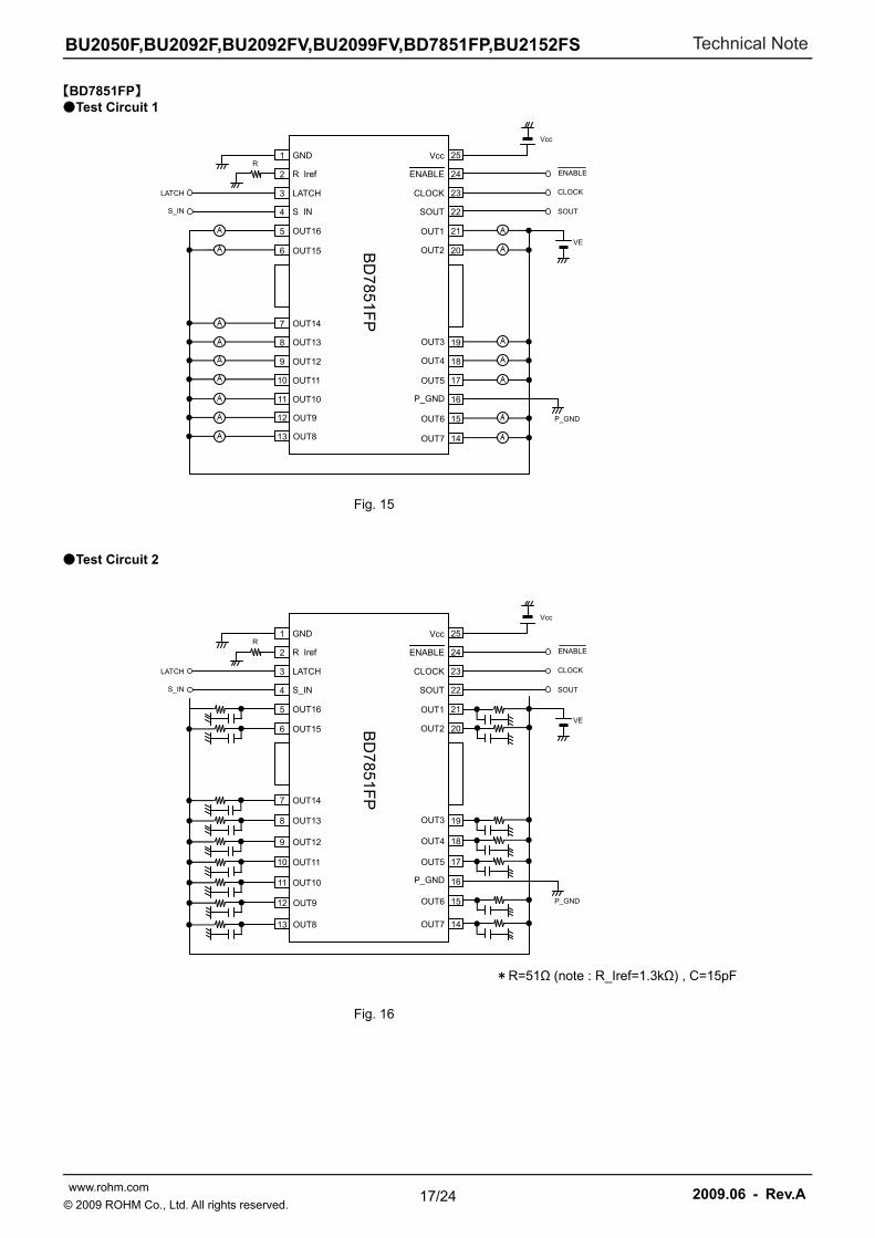
【BD7851FP】 Test Circuit 1
Fig. 15
Test Circuit 2
*R=51Ω (note : R_Iref=1.3kΩ) , C=15pF
Fig. 16
1
2
3
4
5
6
7
8
9
10
11
12
13
19
18
17
16
15
14
25
24
23
22
21
20BD
7851FP
GND
R_Iref
LATCH
S_IN
OUT16
OUT15
OUT14
OUT13
OUT12
OUT11
OUT10
OUT9
OUT8 OUT7
OUT6
P_GND
OUT5
OUT4
OUT3
OUT2
OUT1
SOUT
CLOCK
ENABLE
Vcc
Vcc
ENABLE
SOUT
CLOCK
VE
P_GND
S_IN
LATCH
R
1
2
3
4
5
6
7
8
9
10
11
12
13
19
18
17
16
15
14
25
24
23
22
21
20BD
7851FP
GND
R_Iref
LATCH
S_IN
OUT16
OUT15
OUT14
OUT13
OUT12
OUT11
OUT10
OUT9
OUT8 OUT7
OUT6
P_GND
OUT5
OUT4
OUT3
OUT2
OUT1
SOUT
CLOCK
ENABLE
Vcc
Vcc
ENABLE
SOUT
CLOCK
VE
P_GND
S_IN
LATCH
R
BU2050F,BU2092F,BU2092FV,BU2099FV,BD7851FP,BU2152FS Technical Note
18/24 www.rohm.com 2009.06 - Rev.A
© 2009 ROHM Co., Ltd. All rights reserved.
【BD7851FP】 Switching Time Test Waveforms
Fig. 17
CLOCK
tSU
0.2×VCC
th
tWh tr
0.8×VCC 0.8×VCC
0.2×VCC
tf
0.8×VCC
S_IN
0.8×VCC 0.8×VCC
LATCH
th
twh
0.8×VCC
0.2×VCC
tSU
OUTn
90%
10%
tpHL・tpLH
90%
10%
tpHL
tf
tpHL
90%
10%
tr
ENABLE 0.2×VCC
0.8×VCC
tw
SOUT
0.8×VCC
0.2×VCC
tpHL・tpLH
tf・tr
BU2050F,BU2092F,BU2092FV,BU2099FV,BD7851FP,BU2152FS Technical Note
19/24 www.rohm.com 2009.06 - Rev.A
© 2009 ROHM Co., Ltd. All rights reserved.
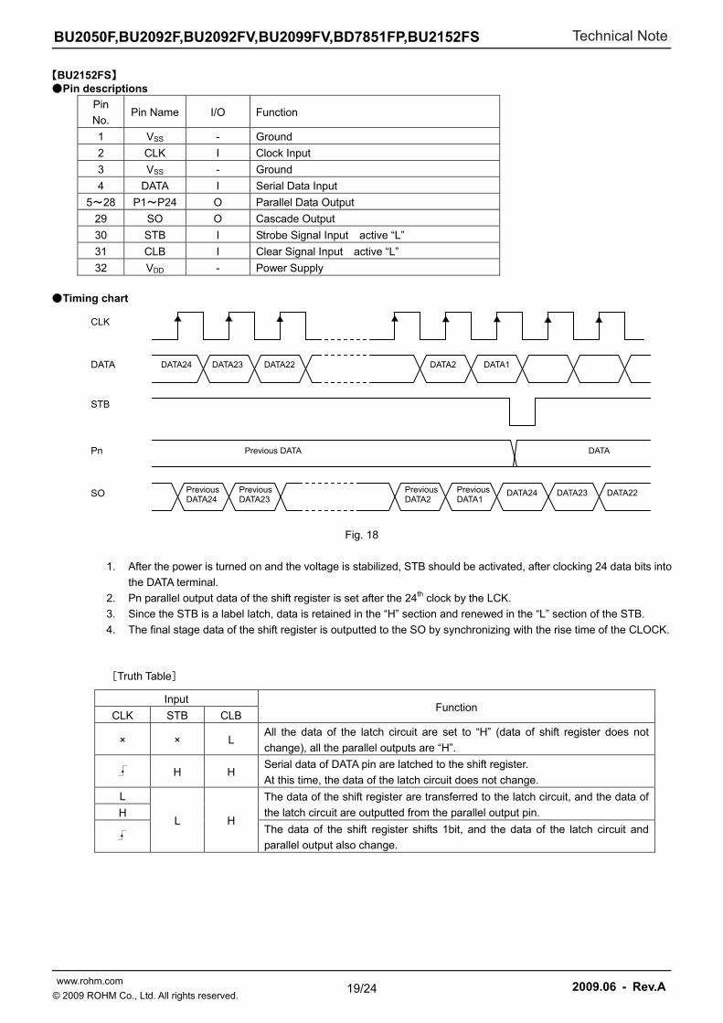
【BU2152FS】 Pin descriptions
Pin
No. Pin Name I/O Function
1 VSS - Ground
2 CLK I Clock Input
3 VSS - Ground
4 DATA I Serial Data Input
5~28 P1~P24 O Parallel Data Output
29 SO O Cascade Output
30 STB I Strobe Signal Input active “L”
31 CLB I Clear Signal Input active “L”
32 VDD - Power Supply
Timing chart
Fig. 18
1. After the power is turned on and the voltage is stabilized, STB should be activated, after clocking 24 data bits into
the DATA terminal.
2. Pn parallel output data of the shift register is set after the 24th clock by the LCK.
3. Since the STB is a label latch, data is retained in the “H” section and renewed in the “L” section of the STB.
4. The final stage data of the shift register is outputted to the SO by synchronizing with the rise time of the CLOCK.
[Truth Table]
Input Function
CLK STB CLB
× × L All the data of the latch circuit are set to “H” (data of shift register does not
change), all the parallel outputs are “H”.
H H
Serial data of DATA pin are latched to the shift register.
At this time, the data of the latch circuit does not change.
L
L H
The data of the shift register are transferred to the latch circuit, and the data of
the latch circuit are outputted from the parallel output pin. H
The data of the shift register shifts 1bit, and the data of the latch circuit and
parallel output also change.
CLK
STB
DATA DATA24 DATA23 DATA22 DATA2 DATA1
SO Previous DATA24
Previous DATA23
Previous DATA2
DATA24 Previous DATA1
DATA23 DATA22
Pn Previous DATA DATA

BU2050F,BU2092F,BU2092FV,BU2099FV,BD7851FP,BU2152FS Technical Note
20/24 www.rohm.com 2009.06 - Rev.A
© 2009 ROHM Co., Ltd. All rights reserved.
【BU2152FS】 Switching characteristics (Unless otherwise specified, VDD=2.7 to 5.5V, VSS=0V, Ta=25)
Parameter Symbol Limit
Unit Condition Min. Typ. Max.
Maximum Clock Frequency fMAX 5 - - MHz
Setup Time 1 tSU1 20 - - ns DATA-CLK
Hold Time 1 tHD1 20 - - ns CLK-DATA
Setup Time 2 tSU2 30 - - ns STB-CLK
Hold Time 2 tHD2 30 - - ns CLK-STB
Setup Time 3 tSU3 30 - - ns CLB-CLK
Hold Time 3 tHD3 30 - - ns CLK-CLB
Setup Time 4 tSU4 30 - - ns STB-CLB
Hold Time 4 tHD4 30 - - ns CLB-STB
Output Delay Time 1* tPD1 - - 100 ns CLK-P1~P24
Output Delay Time 2* tPD2 - - 80 ns STB-P1~P24
Output Delay Time 3* tPD3. - - 80 ns CLB-P1~P24
*50pF of load is attached.

BU2050F,BU2092F,BU2092FV,BU2099FV,BD7851FP,BU2152FS Technical Note
21/24 www.rohm.com 2009.06 - Rev.A
© 2009 ROHM Co., Ltd. All rights reserved.
Switching characteristic conditions Setup/Hold Time (DATA-CLOCK, STB-CLOCK, CLB-CLOCK)
Setup/Hold Time (STB-CLB)
Fig. 19 Switching characteristic conditions 1
Output Delay Time (CLOCK-P1~P24)
Output Delay Time (STB-P1~P24)
Output Delay Time (CLB-P1~P24)
Fig. 20 Switching characteristic conditions 2
CLOCK
90%
10%
tr
50%
90%
10%
tr
50%
50%50%
tSU1
tHD1
tHD2 tSU2
50%50%
tHD3 tSU3
DATA
STB
CLB
50%CLB
tSU4 tHD4
STB
50%
tPD1
CLOCK
P1~P24
50%
STB
P1~P24
tPD2
50%
CLB
50%
tPD3

BU2050F,BU2092F,BU2092FV,BU2099FV,BD7851FP,BU2152FS Technical Note
22/24 www.rohm.com 2009.06 - Rev.A
© 2009 ROHM Co., Ltd. All rights reserved.
Notes for use
1. Absolute maximum ratings
An excess in the absolute maximum ratings, such as supply voltage, temperature range of operating conditions, etc., can
break down the devices, thus making impossible to identify breaking mode, such as a short circuit or an open circuit. If any
over rated values will expect to exceed the absolute maximum ratings, consider adding circuit protection devices, such as
fuses.
2. Connecting the power supply connector backward
Connecting of the power supply in reverse polarity can damage IC. Take precautions when connecting the power supply
lines. An external direction diode can be added.
3. Power supply lines
Design PCB layout pattern to provide low impedance GND and supply lines. To obtain a low noise ground and supply line,
separate the ground section and supply lines of the digital and analog blocks. Furthermore, for all power supply terminals to
ICs, connect a capacitor between the power supply and the GND terminal. When applying electrolytic capacitors in the circuit,
not that capacitance characteristic values are reduced at low temperatures.
4. GND voltage
The potential of GND pin must be minimum potential in all operating conditions.
5. Thermal design
Use a thermal design that allows for a sufficient margin in light of the power dissipation (Pd) in actual operating conditions.
6. Inter-pin shorts and mounting errors
Use caution when positioning the IC for mounting on printed circuit boards. The IC may be damaged if there is any
connection error or if pins are shorted together.
7. Actions in strong electromagnetic field
Use caution when using the IC in the presence of a strong electromagnetic field as doing so may cause the IC to malfunction.
8. Testing on application boards
When testing the IC on an application board, connecting a capacitor to a pin with low impedance subjects the IC to stress.
Always discharge capacitors after each process or step. Always turn the IC's power supply off before connecting it to or
removing it from a jig or fixture during the inspection process. Ground the IC during assembly steps as an antistatic measure.
Use similar precaution when transporting or storing the IC.
9. Ground Wiring Pattern
When using both small signal and large current GND patterns, it is recommended to isolate the two ground patterns, placing
a single ground point at the ground potential of application so that the pattern wiring resistance and voltage variations caused
by large currents do not cause variations in the small signal ground voltage. Be careful not to change the GND wiring pattern
of any external components, either.
10. Unused input terminals
Connect all unused input terminals to VDD or VSS in order to prevent excessive current or oscillation.
Insertion of a resistor (100kΩ approx.) is also recommended.

BU2050F,BU2092F,BU2092FV,BU2099FV,BD7851FP,BU2152FS Technical Note
23/24 www.rohm.com 2009.06 - Rev.A
© 2009 ROHM Co., Ltd. All rights reserved.
Ordering part number
B U 2 0 9 2 F V - E 2
Part No. Part No. 2050 2092 2099 7851 2152
Package F : SOP14 : SOP18 FV : SSOP-B20 FP : HSOP25 FS : SSOP-A32
Packaging and forming specification E2: Embossed tape and reel
(Unit : mm)
SOP14
7
14
1.27
0.11
1
8
0.3M
IN
8.7±0.2
0.4±0.1
0.15±0.1
1.5
±0.1
6.2
±0.3
4.4
±0.2
(MAX 9.05 include BURR)
0.1
∗ Order quantity needs to be multiple of the minimum quantity.
<Tape and Reel information>
Embossed carrier tapeTape
Quantity
Direction of feed
The direction is the 1pin of product is at the upper left when you hold reel on the left hand and you pull out the tape on the right hand
2500pcs
E2
( )
Direction of feed
Reel1pin
(Unit : mm)
SOP18
18
0.3M
IN
1.27
91
10
11.2±0.2
0.15±0.1
0.4±0.1
7.8
±0.3
1.8
±0.1
0.11
5.4
±0.2
(MAX 11.55 include BURR)
0.1
∗ Order quantity needs to be multiple of the minimum quantity.
<Tape and Reel information>
Embossed carrier tapeTape
Quantity
Direction of feed
The direction is the 1pin of product is at the upper left when you hold reel on the left hand and you pull out the tape on the right hand
2000pcs
E2
( )
Direction of feed
Reel1pin
(Unit : mm)
SSOP-B20
0.1
11
10
20
1
0.1±
0.1
6.4
± 0.
3
4.4
± 0.
2
6.5 ± 0.2
0.15 ± 0.1
0.22 ± 0.1
0.65
1.15
± 0
.1
0.3M
in.
∗ Order quantity needs to be multiple of the minimum quantity.
<Tape and Reel information>
Embossed carrier tapeTape
Quantity
Direction of feed
The direction is the 1pin of product is at the upper left when you hold reel on the left hand and you pull out the tape on the right hand
2500pcs
E2
( )
Direction of feed
Reel1pin

BU2050F,BU2092F,BU2092FV,BU2099FV,BD7851FP,BU2152FS Technical Note
24/24 www.rohm.com 2009.06 - Rev.A
© 2009 ROHM Co., Ltd. All rights reserved.
∗ Order quantity needs to be multiple of the minimum quantity.
<Tape and Reel information>
Embossed carrier tapeTape
Quantity
Direction of feed
The direction is the 1pin of product is at the upper left when you hold reel on the left hand and you pull out the tape on the right hand
2000pcs
E2
( )
Direction of feed
Reel1pin
(Unit : mm)
SSOP-A32
1
17
16
32
0.11
0.3M
IN
0.36±0.10.8
13.6±0.2
0.15±0.1
5.4
±0.2
7.8
±0.3
1.8
±0.1
(MAX 13.95 include BURR)
0.1
(Unit : mm)
HSOP257.
8 ±
0.3
5.4
± 0.
2
2.75 ± 0.1
1.95 ± 0.1
25 14
1 13
0.111.
9 ±
0.1
0.36 ± 0.1
12.0 ± 0.2
0.3M
in.
0.25 ± 0.1
13.6 ± 0.2
0.8
(MAX 13.95 include BURR)
S
0.1 S
∗ Order quantity needs to be multiple of the minimum quantity.
<Tape and Reel information>
Embossed carrier tapeTape
Quantity
Direction of feed
The direction is the 1pin of product is at the upper left when you hold reel on the left hand and you pull out the tape on the right hand
2000pcs
E2
( )
Direction of feed
Reel1pin

R0039Awww.rohm.com© 2009 ROHM Co., Ltd. All rights reserved.
Notice
ROHM Customer Support Systemhttp://www.rohm.com/contact/
Thank you for your accessing to ROHM product informations. More detail product informations and catalogs are available, please contact us.
No t e s
No copying or reproduction of this document, in part or in whole, is permitted without the consent of ROHM Co.,Ltd.
The content specified herein is subject to change for improvement without notice.
The content specified herein is for the purpose of introducing ROHM's products (hereinafter "Products"). If you wish to use any such Product, please be sure to refer to the specifications, which can be obtained from ROHM upon request.
Examples of application circuits, circuit constants and any other information contained herein illustrate the standard usage and operations of the Products. The peripheral conditions must be taken into account when designing circuits for mass production.
Great care was taken in ensuring the accuracy of the information specified in this document. However, should you incur any damage arising from any inaccuracy or misprint of such information, ROHM shall bear no responsibility for such damage.
The technical information specified herein is intended only to show the typical functions of and examples of application circuits for the Products. ROHM does not grant you, explicitly or implicitly, any license to use or exercise intellectual property or other rights held by ROHM and other parties. ROHM shall bear no responsibility whatsoever for any dispute arising from the use of such technical information.
The Products specified in this document are intended to be used with general-use electronic equipment or devices (such as audio visual equipment, office-automation equipment, commu-nication devices, electronic appliances and amusement devices).
The Products specified in this document are not designed to be radiation tolerant.
While ROHM always makes efforts to enhance the quality and reliability of its Products, a Product may fail or malfunction for a variety of reasons.
Please be sure to implement in your equipment using the Products safety measures to guard against the possibility of physical injury, fire or any other damage caused in the event of the failure of any Product, such as derating, redundancy, fire control and fail-safe designs. ROHM shall bear no responsibility whatsoever for your use of any Product outside of the prescribed scope or not in accordance with the instruction manual.
The Products are not designed or manufactured to be used with any equipment, device or system which requires an extremely high level of reliability the failure or malfunction of which may result in a direct threat to human life or create a risk of human injury (such as a medical instrument, transportation equipment, aerospace machinery, nuclear-reactor controller, fuel-controller or other safety device). ROHM shall bear no responsibility in any way for use of any of the Products for the above special purposes. If a Product is intended to be used for any such special purpose, please contact a ROHM sales representative before purchasing.
If you intend to export or ship overseas any Product or technology specified herein that may be controlled under the Foreign Exchange and the Foreign Trade Law, you will be required to obtain a license or permit under the Law.