sequence detector
DESCRIPTION
Design and implementation of a sequence detectorTRANSCRIPT
UNIVERSITY OF MAURITIUS
Faculty of Engineering
Dept of Electrical and Electronic Engineering
Electronic System Design (3005Y)
Assignment
Sequence Detector
Date submitted: 4th March 2013
Name: BADULLA Mushood Yaahya ID: 1011907 EEE
Name: KISTO Nandraj ID: 1010095 ECE
Name: LI KAM SHUN Brandon ID: 1014730 EEE
Name: RAJUBALLY Arshad ID: 1012188 EEE
Team: 9
SAMPLE

ii
TABLE OF CONTENTS
1. Introduction 1
2. Objectives 2
3. Machine design 3
3.1. Moore state diagram 3
3.2. Mealy state diagram 4
3.3. Moore state table 5
3.4. State minimisation 5
3.5. State assignment 6
3.6 State transition table 7
4. Implementation using combinational logic and memory
elements
8
4.1. Derivation of state equations 8
4.2. Multisim simulation 9
5. Implementation using a registered field programmable
logic arrays
10
5.1. Product terms 10
5.2. Personality matrix 12
SAMPLE
iii
5.3. RPLA representation 13
6. Implementation using generic array logic 14
6.1. WinCupl design file 14
6.2. Symbol table 16
6.3. Fuse plot 17
6.4. Chip diagram 19
6.5. Final circuit 20
7. Conclusion 21
8. References 22
SAMPLE

1
INTRODUCTION
A sequence detector is to be designed and implemented. The sequence detector has two
input lines, x1 and x2 and one output line. The machine produces an output 1 if the
sequence 101 is detected on the x1 line and with x2 remaining 1 for all 3 bits. Once the
output is 1, it remains 1 until x2 becomes zero.
This report presents the design process of the sequence detector and the implementation
of the sequence detector. The sequence detector was implemented by the following
methods: combinational and logic elements, registered field programmable logic arrays,
generic array logic.
The hardware implementation of the sequence detector was carried out for the generic
array logic system along with the WinCUPL design.
SAMPLE

2
CHAPTER 2: OBJECTIVES
The sequence detector clock mode machine has two input lines, x1 and x2 and one
output line. The machine produces an output 1 if the sequence 101 is detected on the x1
line and with x2 remaining 1 for all 3 bits. Once the output is 1, it remains 1 until x2
becomes zero. The objectives of this assignment are:
• To derive the Moore state diagram of the machine
• To convert the Moore machine into a Mealy machine
• To minimise the Moore machine into a minimum state machine
• To implement the machine with combinational logic and memory elements
• To implement the machine using registered field programmable logic arrays
• To implement the machine using generic array logic, WINCUPL to be used to
write the design file
• To show the hardware implementation of the GAL system
SAMPLE
3
CHAPTER 3: MACHINE DESIGN
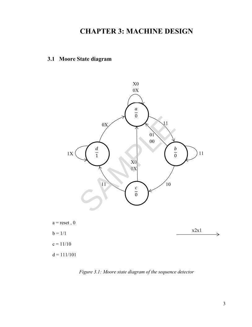
3.1 Moore State diagram
Figure 3.1: Moore state diagram of the sequence detector
�
0
�
0
�
0
�
1
11 0X
11 10
X0
0X
11
1X
X0
0X
01
00
x2x1
a = reset , 0
b = 1/1
c = 11/10
d = 111/101
SAMPLE
4
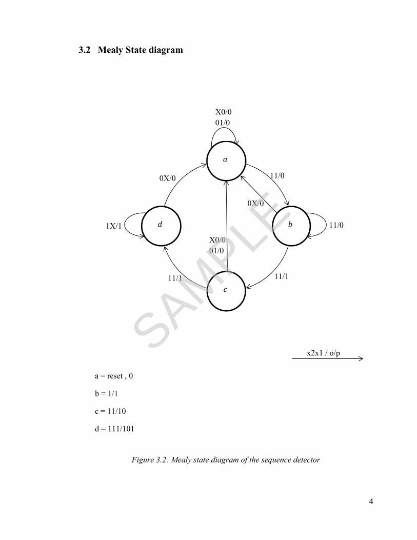
3.2 Mealy State diagram
Figure 3.2: Mealy state diagram of the sequence detector
�
�
�
�
11/0 0X/0
11/1 11/1
X0/0
01/0
11/0
1X/1
X0/0
01/0
0X/0
x2x1 / o/p
a = reset , 0
b = 1/1
c = 11/10
d = 111/101
SAMPLE

5
3.3 Moore State table
Present
State
Next state, x2x1=
o/p 00 01 10 11
a a a a b 0
b a a c b 0
c a a a d 0
d a a d d 1
3.4 State Minimisation
b ac
c bd ac
d X X X
a b c
The Moore machine is already a minimum state machine.
SAMPLE
6
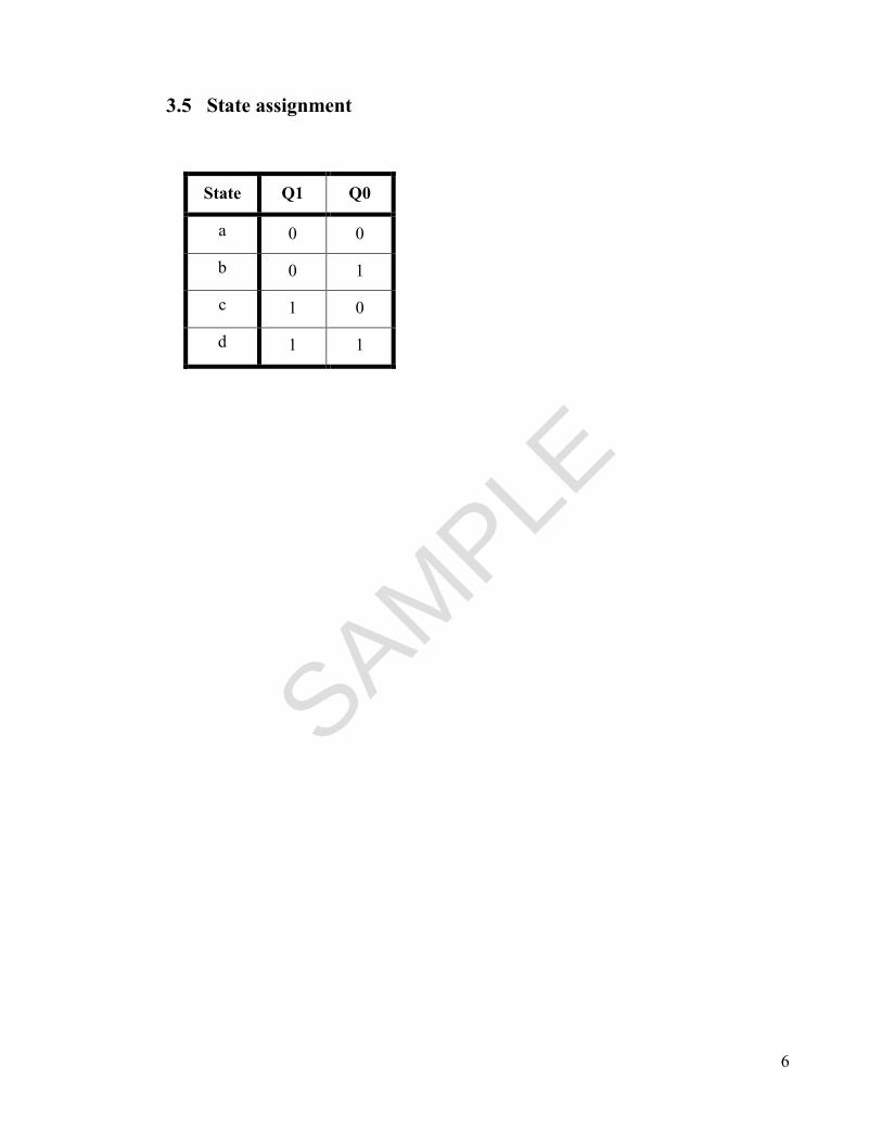
3.5 State assignment
State Q1 Q0
a 0 0
b 0 1
c 1 0
d 1 1
SAMPLE
7
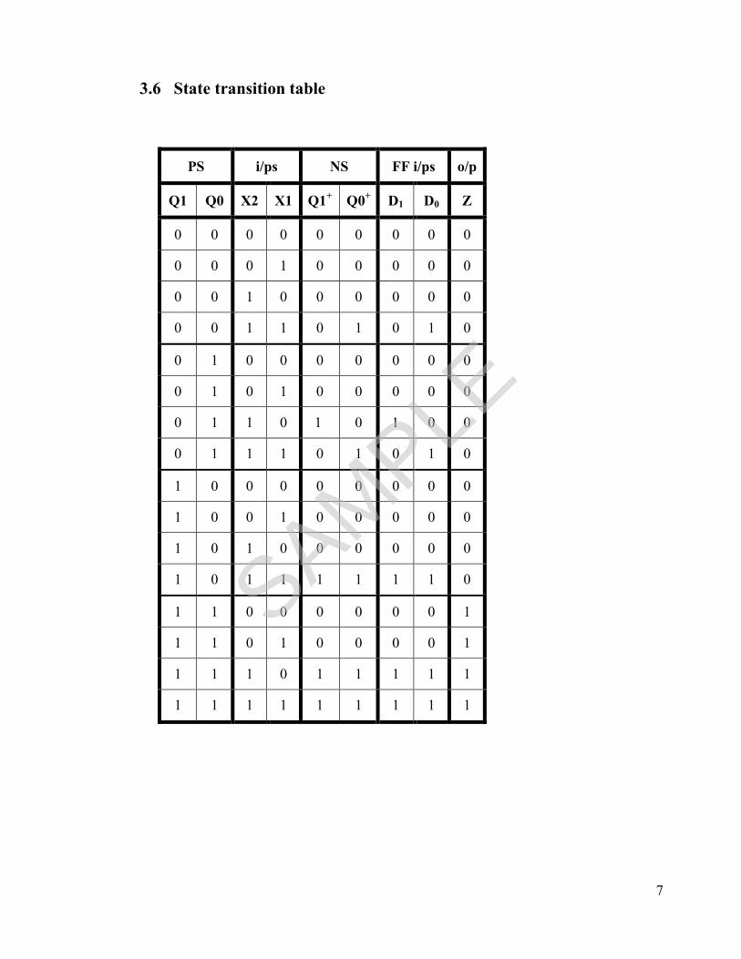
3.6 State transition table
PS i/ps NS FF i/ps o/p
Q1 Q0 X2 X1 Q1+ Q0
+ D1 D0 Z
0 0 0 0 0 0 0 0 0
0 0 0 1 0 0 0 0 0
0 0 1 0 0 0 0 0 0
0 0 1 1 0 1 0 1 0
0 1 0 0 0 0 0 0 0
0 1 0 1 0 0 0 0 0
0 1 1 0 1 0 1 0 0
0 1 1 1 0 1 0 1 0
1 0 0 0 0 0 0 0 0
1 0 0 1 0 0 0 0 0
1 0 1 0 0 0 0 0 0
1 0 1 1 1 1 1 1 0
1 1 0 0 0 0 0 0 1
1 1 0 1 0 0 0 0 1
1 1 1 0 1 1 1 1 1
1 1 1 1 1 1 1 1 1
SAMPLE
8
CHAPTER 4:
IMPLEMENTATION USING COMBINATIONAL
LOGIC AND MEMORY ELEMENTS
4.1 Derivation of the state equations
D1 = ΣM (6,11,14,15)
D0 = ΣM (3,7,11,14,15)
Z = Q1 AND Q0
The sequence detector was implemented using a 4 to 16 decoder, 2 NAND gates, 2 D flip
flops and 1 AND gate.
SAMPLE
9
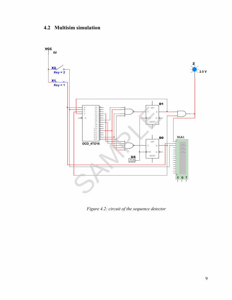
4.2 Multisim simulation
Figure 4.2: circuit of the sequence detector
DCD_4TO16
ABC
~G
D
Y0Y1Y2
Y4Y3
Y5Y6Y7Y8Y9Y10Y11Y12Y13Y14Y15
D1
D Q
~Q
RESET
CLK
SET
D0
D Q
~Q
RESET
CLK
SET
VCC
5V
Z
2.5 V
X2
Key = 2
X1
Key = 1
U4
XLA1
C Q T
1
F
SAMPLE
10
CHAPTER 5:
IMPLEMENTATION USING A REGISTERED
FIELD PROGRAMMABLE LOGIC ARRAYS
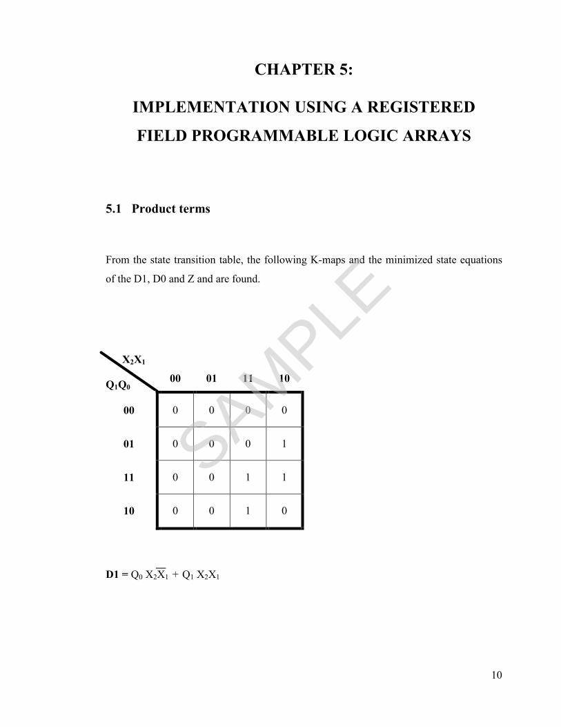
5.1 Product terms
From the state transition table, the following K-maps and the minimized state equations
of the D1, D0 and Z and are found.
X2X1
Q1Q0……
00
01
11
10
00 0 0 0 0
01 0 0 0 1
11 0 0 1 1
10 0 0 1 0
D1 = Q0 X2X1 + Q1 X2X1
SAMPLE
11
X2X1
Q1Q0……
00
01
11
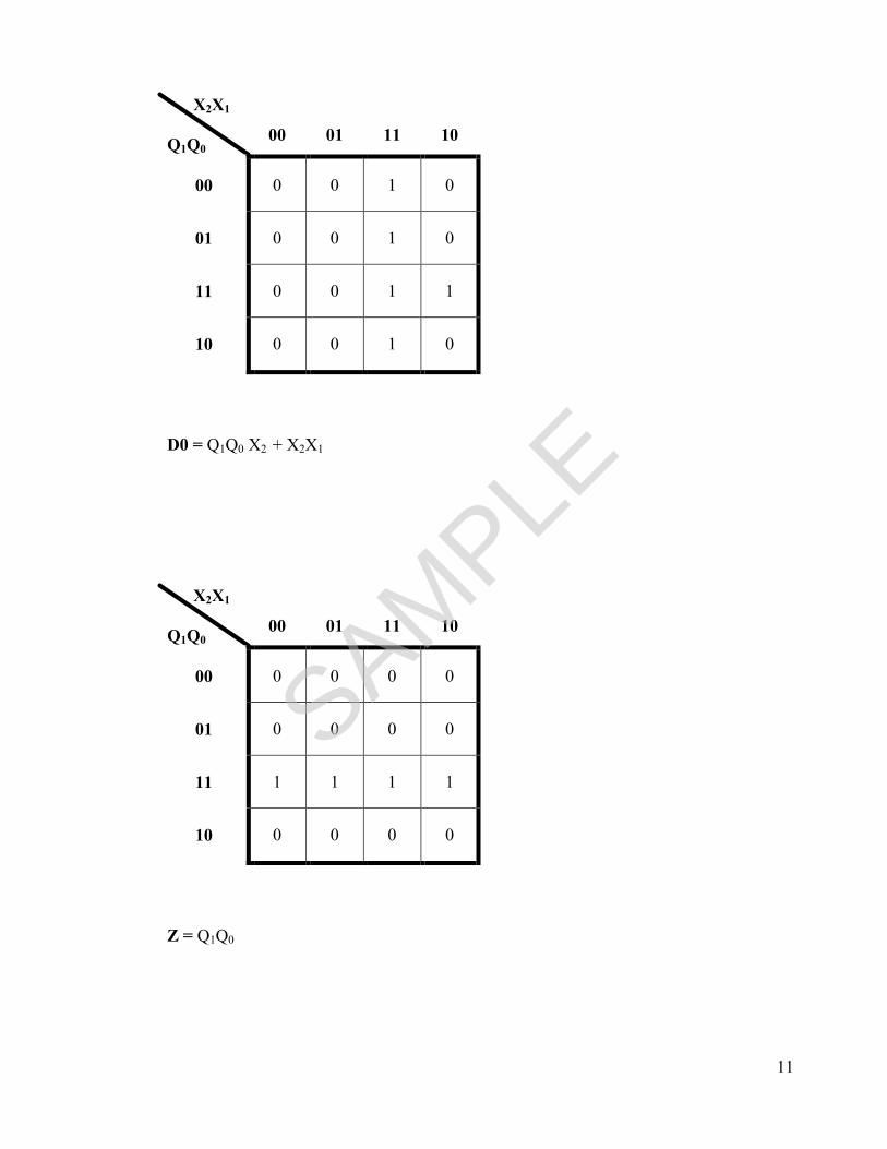
10
00 0 0 1 0
01 0 0 1 0
11 0 0 1 1
10 0 0 1 0
D0 = Q1Q0 X2 + X2X1
X2X1
Q1Q0……
00
01
11
10
00 0 0 0 0
01 0 0 0 0
11 1 1 1 1
10 0 0 0 0
Z = Q1Q0
SAMPLE
12
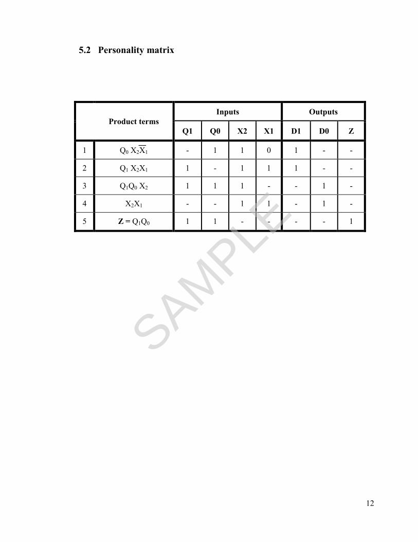
5.2 Personality matrix
Product terms
Inputs Outputs
Q1 Q0 X2 X1 D1 D0 Z
1 Q0 X2X1 - 1 1 0 1 - -
2 Q1 X2X1 1 - 1 1 1 - -
3 Q1Q0 X2 1 1 1 - - 1 -
4 X2X1 - - 1 1 - 1 -
5 Z = Q1Q0 1 1 - - - - 1
SAMPLE
13
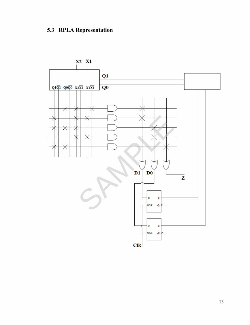
5.3 RPLA Representation
SAMPLE
14
CHAPTER 6:
IMPLEMENTATION USING GENERIC ARRAY
LOGIC
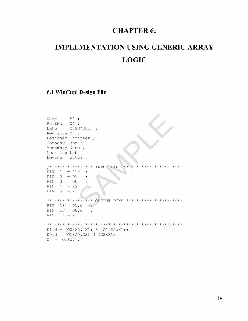
6.1 WinCupl Design File
Name A2 ; PartNo 00 ; Date 2/23/2013 ; Revision 01 ; Designer Engineer ; Company uom ; Assembly None ; Location Lab ; Device g16v8 ; /* *************** INPUT PINS *********************/ PIN 1 = Clk ; PIN 2 = Q1 ; PIN 3 = Q0 ; PIN 4 = X2 ; PIN 5 = X1 ; /* *************** OUTPUT PINS *********************/ PIN 12 = D1.d ; PIN 13 = D0.d ; PIN 14 = Z ; /* *************************************************/ D1.d = (Q0&X2&!X1) # (Q1&X2&X1); D0.d = (Q1&Q0&X2) # (X2&X1); Z = (Q1&Q0);
SAMPLE

15
****************************************************************************** A2 ******************************************************************************* CUPL(WM) 5.0a Serial# 60008009 Device g16v8ms Library DLIB-h-40-11 Created Mon Feb 25 19:38:01 2013 Name A2 Partno 00 Revision 01 Date 2/23/2013 Designer Engineer Company uom Assembly None Location Lab =============================================================================== Expanded Product Terms =============================================================================== D0 => Q0 & Q1 & X2 # X1 & X2 D1 => Q0 & !X1 & X2 # Q1 & X1 & X2 Z => Q0 & Q1 Z.oe => 1
SAMPLE
16
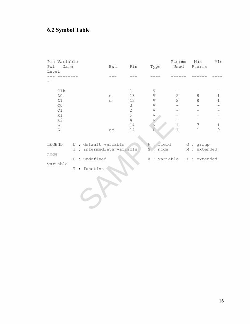
6.2 Symbol Table
Pin Variable Pterms Max Min Pol Name Ext Pin Type Used Pterms Level --- -------- --- --- ---- ------ ------ ----- Clk 1 V - - - D0 d 13 V 2 8 1 D1 d 12 V 2 8 1 Q0 3 V - - - Q1 2 V - - - X1 5 V - - - X2 4 V - - - Z 14 V 1 7 1 Z oe 14 D 1 1 0 LEGEND D : default variable F : field G : group I : intermediate variable N : node M : extended node U : undefined V : variable X : extended variable T : function
SAMPLE
17
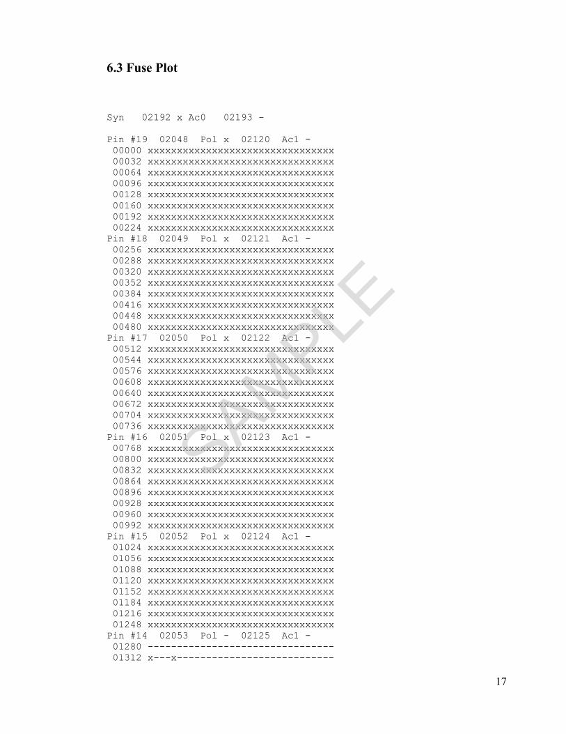
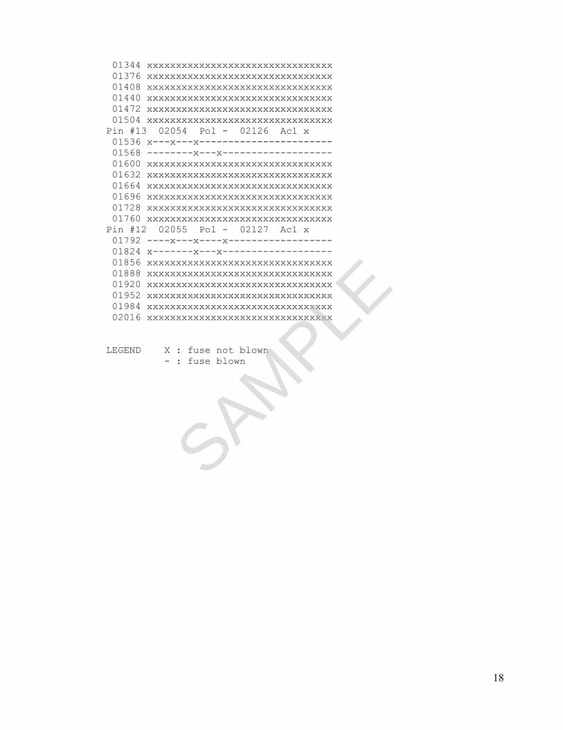
6.3 Fuse Plot
Syn 02192 x Ac0 02193 - Pin #19 02048 Pol x 02120 Ac1 - 00000 xxxxxxxxxxxxxxxxxxxxxxxxxxxxxxxx 00032 xxxxxxxxxxxxxxxxxxxxxxxxxxxxxxxx 00064 xxxxxxxxxxxxxxxxxxxxxxxxxxxxxxxx 00096 xxxxxxxxxxxxxxxxxxxxxxxxxxxxxxxx 00128 xxxxxxxxxxxxxxxxxxxxxxxxxxxxxxxx 00160 xxxxxxxxxxxxxxxxxxxxxxxxxxxxxxxx 00192 xxxxxxxxxxxxxxxxxxxxxxxxxxxxxxxx 00224 xxxxxxxxxxxxxxxxxxxxxxxxxxxxxxxx Pin #18 02049 Pol x 02121 Ac1 - 00256 xxxxxxxxxxxxxxxxxxxxxxxxxxxxxxxx 00288 xxxxxxxxxxxxxxxxxxxxxxxxxxxxxxxx 00320 xxxxxxxxxxxxxxxxxxxxxxxxxxxxxxxx 00352 xxxxxxxxxxxxxxxxxxxxxxxxxxxxxxxx 00384 xxxxxxxxxxxxxxxxxxxxxxxxxxxxxxxx 00416 xxxxxxxxxxxxxxxxxxxxxxxxxxxxxxxx 00448 xxxxxxxxxxxxxxxxxxxxxxxxxxxxxxxx 00480 xxxxxxxxxxxxxxxxxxxxxxxxxxxxxxxx Pin #17 02050 Pol x 02122 Ac1 - 00512 xxxxxxxxxxxxxxxxxxxxxxxxxxxxxxxx 00544 xxxxxxxxxxxxxxxxxxxxxxxxxxxxxxxx 00576 xxxxxxxxxxxxxxxxxxxxxxxxxxxxxxxx 00608 xxxxxxxxxxxxxxxxxxxxxxxxxxxxxxxx 00640 xxxxxxxxxxxxxxxxxxxxxxxxxxxxxxxx 00672 xxxxxxxxxxxxxxxxxxxxxxxxxxxxxxxx 00704 xxxxxxxxxxxxxxxxxxxxxxxxxxxxxxxx 00736 xxxxxxxxxxxxxxxxxxxxxxxxxxxxxxxx Pin #16 02051 Pol x 02123 Ac1 - 00768 xxxxxxxxxxxxxxxxxxxxxxxxxxxxxxxx 00800 xxxxxxxxxxxxxxxxxxxxxxxxxxxxxxxx 00832 xxxxxxxxxxxxxxxxxxxxxxxxxxxxxxxx 00864 xxxxxxxxxxxxxxxxxxxxxxxxxxxxxxxx 00896 xxxxxxxxxxxxxxxxxxxxxxxxxxxxxxxx 00928 xxxxxxxxxxxxxxxxxxxxxxxxxxxxxxxx 00960 xxxxxxxxxxxxxxxxxxxxxxxxxxxxxxxx 00992 xxxxxxxxxxxxxxxxxxxxxxxxxxxxxxxx Pin #15 02052 Pol x 02124 Ac1 - 01024 xxxxxxxxxxxxxxxxxxxxxxxxxxxxxxxx 01056 xxxxxxxxxxxxxxxxxxxxxxxxxxxxxxxx 01088 xxxxxxxxxxxxxxxxxxxxxxxxxxxxxxxx 01120 xxxxxxxxxxxxxxxxxxxxxxxxxxxxxxxx 01152 xxxxxxxxxxxxxxxxxxxxxxxxxxxxxxxx 01184 xxxxxxxxxxxxxxxxxxxxxxxxxxxxxxxx 01216 xxxxxxxxxxxxxxxxxxxxxxxxxxxxxxxx 01248 xxxxxxxxxxxxxxxxxxxxxxxxxxxxxxxx Pin #14 02053 Pol - 02125 Ac1 - 01280 -------------------------------- 01312 x---x---------------------------
SAMPLE
18
01344 xxxxxxxxxxxxxxxxxxxxxxxxxxxxxxxx 01376 xxxxxxxxxxxxxxxxxxxxxxxxxxxxxxxx 01408 xxxxxxxxxxxxxxxxxxxxxxxxxxxxxxxx 01440 xxxxxxxxxxxxxxxxxxxxxxxxxxxxxxxx 01472 xxxxxxxxxxxxxxxxxxxxxxxxxxxxxxxx 01504 xxxxxxxxxxxxxxxxxxxxxxxxxxxxxxxx Pin #13 02054 Pol - 02126 Ac1 x 01536 x---x---x----------------------- 01568 --------x---x------------------- 01600 xxxxxxxxxxxxxxxxxxxxxxxxxxxxxxxx 01632 xxxxxxxxxxxxxxxxxxxxxxxxxxxxxxxx 01664 xxxxxxxxxxxxxxxxxxxxxxxxxxxxxxxx 01696 xxxxxxxxxxxxxxxxxxxxxxxxxxxxxxxx 01728 xxxxxxxxxxxxxxxxxxxxxxxxxxxxxxxx 01760 xxxxxxxxxxxxxxxxxxxxxxxxxxxxxxxx Pin #12 02055 Pol - 02127 Ac1 x 01792 ----x---x----x------------------ 01824 x-------x---x------------------- 01856 xxxxxxxxxxxxxxxxxxxxxxxxxxxxxxxx 01888 xxxxxxxxxxxxxxxxxxxxxxxxxxxxxxxx 01920 xxxxxxxxxxxxxxxxxxxxxxxxxxxxxxxx 01952 xxxxxxxxxxxxxxxxxxxxxxxxxxxxxxxx 01984 xxxxxxxxxxxxxxxxxxxxxxxxxxxxxxxx 02016 xxxxxxxxxxxxxxxxxxxxxxxxxxxxxxxx LEGEND X : fuse not blown - : fuse blown
SAMPLE
19
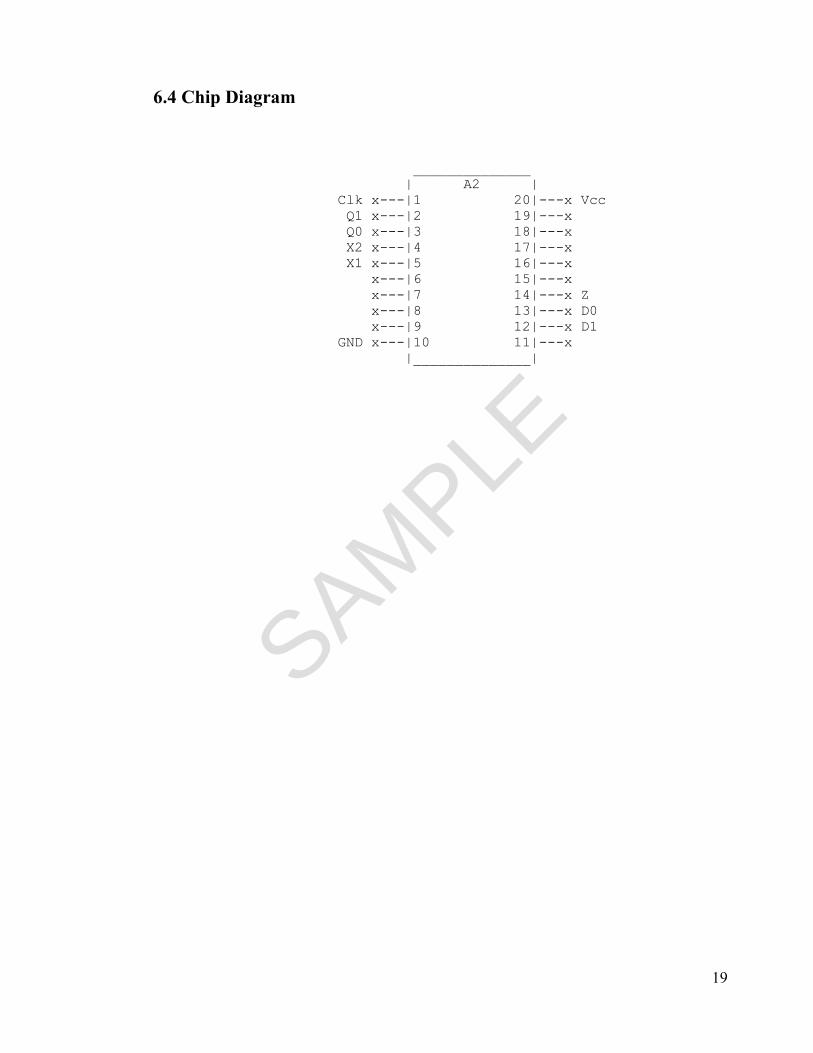
6.4 Chip Diagram
______________ | A2 | Clk x---|1 20|---x Vcc Q1 x---|2 19|---x Q0 x---|3 18|---x X2 x---|4 17|---x X1 x---|5 16|---x x---|6 15|---x x---|7 14|---x Z x---|8 13|---x D0 x---|9 12|---x D1 GND x---|10 11|---x |______________|
SAMPLE
20
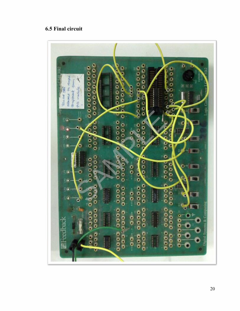
6.5 Final circuit
SAMPLE
21
CONCLUSION
Three different methods to implement the sequence detector have been presented and
discussed in this report. Firstly combinational logic and memory elements were used.
Secondly, the sequence detector was designed using a RPLA. Finally, the sequence
detector was implemented using generic array logic. The WinCupl design file was
written, and the g16v8 PLD was used for the hardware implementation. The sequence
detector was successfully implemented using the g16v8 PLD.
SAMPLE
22
REFERENCES
[1] Lecture notes
[2] A.K Maini, “Programmable Logic Devices,” in Digital Electronics, 1st ed. West
Sussex, England: John Wiley & Sons, 2007, ch. 9, pp. 318–374.
[3] CUPL Programmer’s Reference Guide, 2nd ed. Denver, USA: Logical Devices,
1997
[4] Floyd and Jain, “Programmable Logic Devices,” in Digital Fundamentals, 8th ed.
New Delhi, India: Pearson Education, 2009, ch. 12, pp. 441–469.
[5] GAL16V8 Datasheet, available from:
http://www.atmel.com/Images/doc0364.pdf
SAMPLE