sensortape: modular and programmable 3d-aware … strips are cuttable and employ the same form...
TRANSCRIPT

SensorTape: Modular and Programmable 3D-Aware DenseSensor Network on a Tape
Artem DementyevMIT Media Lab
Cambridge, MA, [email protected]
Hsin-Liu (Cindy) KaoMIT Media Lab
Cambridge, MA, [email protected]
Joseph A. ParadisoMIT Media Lab
Cambridge, MA, [email protected]
ABSTRACTSensorTape is a modular and dense sensor network in a formfactor of a tape. SensorTape is composed of interconnectedand programmable sensor nodes on a flexible electronics sub-strate. Each node can sense its orientation with an inertialmeasurement unit, allowing deformation self-sensing of thewhole tape. Also, nodes sense proximity using time-of-flightinfrared. We developed network architecture to automaticallydetermine the location of each sensor node, as SensorTape iscut and rejoined. Also, we made an intuitive graphical inter-face to program the tape. Our user study suggested that Sen-sorTape enables users with different skill sets to intuitivelycreate and program large sensor network arrays. We devel-oped diverse applications ranging from wearables to homesensing, to show low deployment effort required by the user.We showed how SensorTape could be produced at scale usingcurrent technologies and we made a 2.3-meter long prototype.
Author KeywordsSensor tape; cuttable; dense sensor network; self-sensing;flexible electronics
ACM Classification KeywordsH.5.m. Information Interfaces and Presentation (e.g. HCI):Miscellaneous
INTRODUCTIONWe envision a sensate material in the form factor of a tape.Like a roll of ScotchTM tape, it is ubiquitous and inexpensive.It is flexible and cuttable to any length and can be attached toa curved surface. Unlike Scotch tape, it has dense arrays ofdifferent sensors and embedded computation. The tape hasinputs and outputs, and can be programmed and left in theenvironment. The tape is modular, as one can get differenttypes of tape: for example, with inertial measurement units(IMUs), or proximity sensors, or even sensors directly printedon the tape as in [25, 10]. Tapes with different sensors canbe joined together for mixed functionality. Such tape can doself-sensing, so it knows its length, sensor locations, and 3Dshape.
Permission to make digital or hard copies of all or part of this work for personal orclassroom use is granted without fee provided that copies are not made or distributedfor profit or commercial advantage and that copies bear this notice and the full cita-tion on the first page. Copyrights for components of this work owned by others thanACM must be honored. Abstracting with credit is permitted. To copy otherwise, or re-publish, to post on servers or to redistribute to lists, requires prior specific permissionand/or a fee. Request permissions from [email protected] ’15, November 08-11, 2015, Charlotte, NC, USACopyright © 2015 ACM. ISBN 978-1-4503-3779-3/15/11...$15.00.DOI: http://dx.doi.org/10.1145/2807442.2807507
a
b
d
c
e
Figure 1. a) Current flexible circuit prototype, showing electronics oftwo nodes. Each node has a microcontroller, inertial measurement unit(IMU), proximity and light sensors. b) SensorTape can be cut anywhereand rejoined. We develop algorithms to automatically determine theorder and the number of nodes. c) Form factor of SensorTape is of 1-inch wide masking tape. d) SensorTape sensing it’s deformations withIMUs e) The 2.3 meter long testbed with 66 sensor nodes. Proximitysensors are visualized on the laptop, while hovering foot over the tape.
The abilities of sensors to deal with complex phenomena aregreatly increased if they are in dense arrays. For example, anarray of capacitive sensors can track finger on a touchpad oran array of pressure sensors can detect walking patterns in aroom or make an electronic drum. Such sensor arrays havemany applications ranging from engineering to arts, but theyare out of reach for most users. To create them using cur-rent electronics platforms, many discrete modules have to bephysically wired, and a custom communication network hasto be created. This is a time consuming task, and does not al-low easy experimentation, as the network has to be manuallyreprogrammed and rewired when it changes.
A sensor network in the shape of a tape allows for freedomof experimentation. Since tapes and ribbons are familiar ev-eryday materials: the manipulations with the tape are intu-itive. Actions such as cutting and rejoining have direct digital

metaphors. The tape form factor yields well to the currentflexible electronics manufacturing methods. Also, it enablesprecise localization of all sensors, since all the nodes are in alinear array. Sensor nodes can be placed on single communi-cation and power buses, thus removing the need for multiplebatteries and wireless communications.
Current electronics technologies are sufficiently mature forsuch a tape to be made, especially as flexible electronics arebecoming more affordable and prevalent. For example, wehave witnessed emergence of usable and inexpensive LEDstrips e.g. [4]. But so far, LED strips provide only output,and do not have distributed sensing or localization. As elec-tronics are becoming less power hungry, more powerful, andaffordable, it is possible to add such capacities. Even beforethe emergence of such systems, we need to understand theirpotential capacities and how to design them. To do so, wedeveloped the SensorTape platform which enables anyone toexperiment with such a sensate strips. In our implementa-tion, we place programmable and interconnected sensor nodemodules on a flexible substrate, as shown in Figure 1a, and inFigure 4 in detail.
The contributions of the paper are as follows:
1. We introduce a novel sensor network platform in the formfactor of a tape. Such a platform enables fast prototypingand deployment of continuous sensors, as it is modular andcan be cut or joined.
2. We develop a prototype 2.3m long (66 nodes), and a novelself-configurable network architecture. We explain howSensorTape can be manufactured in large quantities.
3. We develop algorithms to demonstrate that SensorTape canbe used for deformation self-sensing (e.g. bend and twist),and measure the accuracy.
4. We evaluate a number of parameters such as cost, speed,power, and maximum length. We conduct user studies tounderstand the usability and possible applications.
5. We explore ways to program such a tape, and implementfour applications to explore use cases.
DESIGN CONSIDERATIONThe sensate tape should meet the following design consider-ations:
1. Employs tape form-factor: The SensorTape should in-herit physical properties of masking tape: it should be cut-table, flexible, and thin. We are inspired by masking tapebecause it is commonly used in craft applications, and thusfamiliar to most users. Masking tape is shown in Figure 1a.
2. Easily configurable: We envision that the tape shouldbe intuitive enough to be manipulated as a traditional craftmaterial. When cutting and joining, the tape should be self-configurable, and know the total number of sensor nodes andthe location of each one. Furthermore, the user should beable to connect the pieces of tape at different angles, for ex-ample to create a rectangular surface. To enable direct userfeedback, the tape should be programmable and have input
and output. A new user interface (UI) should be used to eas-ily program the input and output. The UI can be graphical,leveraging the intuitive tape form factor.
3. High usability: The tape should encourage user’s ex-perimentation. The tape should be able to support a largenumber of sensor nodes without significant bandwidth andpower compromises. As a core sensing modality, the tapeshould sense proximity to physical objects and it’s own bendand twist. Such modalities allow for real-time and tangiblehuman interactions, which facilitate more user experimenta-tion. The tape should be modular to allow addition of nodeswith other sensors. To facilitate physical modifications, thetape should be inexpensive. To reduce the cost, it has to yieldwell to the current manufacturing methods. Communicationprotocol should be robust and able to bypass a broken node.Also, the tape should be physically durable, and able to flexeasily and repeatedly.
PREVIOUS WORKWe are not aware of any projects that explore the tape formfactor to make a modular sensor network. LED strips arecuttable and employ the same form factor, but do not havedistributed computation or sensing capacities. This projecttakes the LED strip concept further to create a modular sen-sor network. Popular electronics platforms (e.g. Arduino) aremostly designed to build discrete devices. Networking 100sof them is beyond the skill and the time frame of many users.Even current modular electronics platforms are not flexibleor cuttable and do not have deformation sensing. They aremostly composed of rigid blocks that snap together. Thiswork draws from four areas, that we categorize below:
Customizable flexible sensors. The technologies [14, 1] toinexpensively and quickly prototype flexible electronics cre-ated a substantial interest in customizable arrays of flexiblesensors. Using paper-like printed circuits, cuttable capaci-tive and resistive sensors were demonstrated in [9, 20, 10, 12]for HCI applications. The work in customizable sensors ismostly concerned with customization of discrete modules.
Dense sensor networks. Most of the research in sensor net-works was done for wireless networks such as Smart Dust[13] or Berkeley’s Mica platform [11]. Wired networks re-ceived less attention. The ChainMail [19] is a sensate-skinsensor network. It is made of rigid circuit board nodes, net-worked with wires. The system does not have deformationsensing ability. Pushpin [17] is a platform for prototypingsensor networks. To provide power each node is pressed intoa multilayer foam-like substrate. Nodes communicate to eachother with infrared signals and can estimate their location.
Substantial work focused on embedding arrays of sensors intoa floor to detect footsteps. For example, Z-tiles [24] usedmodules with pressure sensors, that can network and self-localize. Another work [8] used networked capacitive sensingnodes that were placed on a flexible printed substrate. Thesensor networks above are mostly application specific (e.g.,floor sensing) and do not allow customization and general-purpose use.

Self-sensing surfaces. There has been attempts to createdeformation self-sensing surfaces using piezoelectric sen-sors [23], resistive bend sensors [15] and capacitance [9].ShapeTape (Measurand) is a tape that can sense its bend andtwist, using an array of bundled fiber optic sensors spaced at6 cm. ShapeTape is useful for 3D curve mapping [6], butit is not cuttable or programmable. Many projects in thisspace use machine learning; therefore require retraining if thenumber of sensing elements changes. Our approach is purelyalgorithmic, therefore is scalable to any size. CommercialIMU-based systems (e.g., Xsens MVN, MotionNode) for 3Dmotion tracking are not customizable, bulky, and expensive.
Modular electronics platforms. There has been great in-terest in creating modular electronics platforms [7, 18, 22,26], where one can construct a complex system from modu-lar building blocks. In platforms such as Syftio [18] and Lit-tlebits [7] the rigid modules are snapped together with mag-nets, and communicate through radios or a common bus. Fur-thermore, in the Circuit Stickers platform [21], flexible circuitmodules are attached to paper with copper tape. SeeduinoFilm [3] is an Arduino-based platform composed of rigid-flex PCBs that can be linked together. We are not aware ofany platforms that leverage the flexible tape form factor, orachieve self-sensing.
NETWORK ARCHITECTUREOverview: Our architecture is outlined in Figure 2. The net-work has one master, and all the sensor nodes on the tape areslaves. The master is concerned with coordinating the com-munication and shuttling data to the PC. Each slave contains amicrocontroller (MCU), LEDs and sensors. We used the I2C(Inter-Integrated Circuit) communication bus running at 100kHz to talk between the master and slaves. In I2C slaves andthe master are daisy chained by clock and data wires. Slavescan receive and send data. I2C is often used to talk betweenchips, and was used in some previous work [19, 8, 24].
Slave 1 MCU+sensors
Slave 2 MCU+sensors
P2P P2PMaster
(MCU)
P2P … Slave N MCU+sensors
I2C (2 wires)
Power (2 wires)
PCSerial
MCU
6-Axis IMU
ToF range finder
RGB LED
Light sensor MCU
3-Axis compass
USB transceiver
Bluetooth
Inside slaveInside master
Figure 2. The network is composed of daisy chained slave nodes and onemaster. Each node is connected to the next by 5 wires: clock and datafor I2C, peer-to-peer serial, 5V power and ground.
We were mainly concerned with making the network robust,fast and self-configurable. Although a sequential peer-to-peer(P2P) network is available, we avoided using this topologyfor data communications. With the daisy chain bus topology,if one node goes down, others continue to function. Also,the data rates can be faster since data does not have to hop
through multiple nodes. Specifically we chose I2C bus be-cause the microcontroller has a hardware I2C module, whichmakes it more reliable, since it has a memory buffer and gen-erates accurate clock. Furthermore, I2C only uses two wires,and keeping the number of wires between the nodes to theminimum makes it easier to join pieces of the tape. 1-Wireprotocol (Dallas) requires only one wire for communications,but was avoided due to lack of dedicated hardware and theprotocol’s proprietary standard.
Start
Send ‘0’ to first slave
wait for P2P propagation
wait for an address
Assign address
Search all addresses
Create slave lookup
Poll slaves
Wait for events
Master’s read
request
Sensor’s request
Master’s write
request
StartMaster Slave
Figure 3. Communication flowcharts for the master and a slave. Theevents in gray boxes happen over peer-to-peer communications. Laterevents happen over I2C.
Communication protocol: The communications are out-lined in Figure 3. Each slave has a unique address of 7 bits,allowing 128 total devices. Since each slave needs to havea unique address and the network size can change, the ad-dresses are assigned dynamically. We used the peer-to-peerserial communication to assign the addresses. The master ini-tiates communication by sending 0 to the first slave. The firstslave address is assigned to 0, and the first slave sends 1 tothe second slave. This hopping repeats until the last slave isreached.
After slave address assignment, the master does not knowhow many slaves are present, so it sends a command to allpossible addresses from 0 to 127. If a slave is present, it willreply with the number and type of sensors it has. That allowsthe master to create a directory of all present slaves. After theinitiation, the master polls the slaves in a consecutive orderat 20 ms intervals. Data is immediately sent to the PC overa serial link. Slaves can receive commands from the master,which we use to change slave’s LED colors. The slave code isinterrupt (event) driven, as it reacts to requests from the mas-ter or its IMU or proximity sensor. Such sensors generate aninterrupt when new data is ready.
PROTOTYPESWe constructed two prototypes (Figure 4), each with uniqueadvantages and disadvantages. Both have the same soft-ware and electronics, and only differ in the construction tech-niques. Both work with the same master node, which can beclipped or soldered to the tape. The conductive inkjet pro-totype 1 is easier to experiment with and reproduce by re-searchers and the DIY community. The flexible circuit proto-type 2 uses the same technology as LED strips. It fits better

MicrocontrollerProximity
IMU
Master
Cut linesSolder pads
RGB LED
Prototype 1
Prototype 2
a
b
sensor nodes
Figure 4. (a) The conductive inkjet prototype 1 (top) and the flexible cir-cuit prototype 2 (bottom) are shown next to each other. The electronicsare exactly the same in both prototypes. Master node is connected toprototype 1. The electronics of each node fit into diamond shaped cells,which are shaded in gray. (b) Close up of the electronics in prototype 2,where solder pads on the cut lines allow easy reconnection. The solderpads expose the five global tracks that run on the backside.
with our future vision of the sensate tape. The prototype 2is more fit for mass production, more robust, and has betterperformance, but requires more expensive and longer manu-facturing process.
Prototype 1: conductive inkjet technologyWe first used conductive inkjet technology [1] to make theflexible substrate. In this technology copper is electroplatedon flexible polyester film, and etched using inkjet-printedmask. Similar technique was used in our other researchprojects [9, 20, 10, 8]. Sensor nodes were made from rigidcircuit boards and soldered to the flexible substrate. Nodeswere spaced at 7cm. We could not attach components di-rectly to the substrate, because it only allows one layer, anddoes not have enough resolution for fine-pitched chips, suchas the proximity sensor.
Prototype 2: Flexible Printed CircuitThe second prototype was made using flexible printed circuit(FPC) technology. We used a 2-layer polyimide-based sub-strate. The electronics were directly soldered onto the FPC.The nodes were spaced at 3.5 cm, and tape was 1-inch wide.We applied a white coverlay to make the tape more aesthet-ically appealing, and make the cut lines more visible. Thenumerous solder pads on both sides of the tape allowed easyreconnection of the five tracks that run on the backside. Weused a South China based circuit manufacturer, since the costsfor flexible circuit technology in the USA and Europe are un-feasibly high for many research budgets. Also, we were able
to get ready advice, since the manufacturer had a lot of expe-rience manufacturing LED strips. We employed an assemblyservice to solder the components. The components can be sol-dered by hand using an inexpensive reflow oven. We wouldnot recommend such a path, as it is time consuming and error-prone to solder small components on a flexible circuit board.We achieved only 20% yield with hand soldering.
Cuttable architectureUsing three cuts: vertical (90�), diagonal left to right (45�)and diagonal right to left (135�), allows for versatile arrange-ments. For example 45� and 135� cuts put together will createa 90� degree bend, as can be seen in Figure 6. Soldering thepieces together is the most reliable, while attaching them withconductive Z-axis tape (3M) is the fastest for rapid prototyp-ing. For ease, we labeled the cut lines on the tape. Electron-ics were put in the diamond shaped cells between the cuts, asseen graphically in Figure 6, and physically in Figure 4b.
4
13
1 3
321
+
135o cut 45o cuts
Rotate 90o Join2D surface
cut lines (dashed)cut cutcut
Figure 6. The tape is layed out based on diamond shaped cells. Eachnode is shown in shaded gray. Diamonds allow 45�, 90� and 135� cuts.In this figure we show how the tape can be cut and rejoined to make a90� bend. Using such bends, the tape can be made into a 2D surface.
ComponentsOne sensor node is composed of following parts:
1. Microcontroller Each node has an ATmega328p (Atmel)microcontroller (MCU). We chose this microcontroller be-cause it is compatible with the Arduino platform, which has alarge support base in the DIY community and an easy-to-useprogramming interface. We wanted the users to be able toeasily program the sensor nodes.
2. Sensors: There are three sensors on-board each node. Weadded as many sensors as possible, to explore various usecases: 1) TEMT6000 (Visday) ambient light sensor. 2) AMPU6050 (Invensense), which is a three-axis accelerometerand three-axis gyro chip. It includes integrated motion pro-cessor, so the chip outputs orientation data in quaternions for-mat. We used this feature to sense deformations. 3), VL6180

1 2 3
65 4
7 8
6
Figure 5. Example interaction using the graphical programing interface. 1) Tape with each sensor node shown as a square. Square brightness changesbased on light. Clicking on one of the squares shows available sensors as circles on top. 2) The user can drag and drop the selected sensor. 3) Draggingto the same square, visualizes that sensor. 4) Dragging to another square creates a relation between two sensors. 5) User is asked to set threshold for thesensor. 6) The relationship is shown by the line on the bottom. 7) By moving hand close to the sensor, LED becomes blue. 8) Red when above threshold.
(STMicroelectronics), Time-of-flight (ToF) distance sensor,which measures the time infrared light takes to bounce froman object. The proximity range is up to 20cm, and it is notinfluenced by the color and type of the surface. We did notsee any interference with neighboring proximity sensors.
3. Miscellaneous: Each node has a voltage regulator. It reg-ulates the input voltage that can range from 5V to 3.5V to astable 3.3V. A second voltage regular provides a stable 2.8Vsupply for the proximity sensor. Furthermore, nodes containan LED (WS2812S, Worldsemi) that can output red, greenand blue. The LED can be controlled from the master andprovides visual feedback to the user.
4. Master node: The master node contains the followingparts: The same ATmega328p, a serial-to-USB converter, anda Bluetooth transceiver. The tape can be clipped to the masternode without soldering using a flexible circuit connector.
DEFORMATION SELF-SENSINGAn important feature of the tape is that it can perform self-sensing. In this section, we will describe the algorithm we de-veloped to sense the tape’s position in space. The algorithmmaps the orientation data from IMUs to a kinematic chainmodel and deformations of 3D surface. To create a referenceframe and to remove gravity we convert original quaternionsinto roll pitch, and yaw. We breakdown all deformations intobending (movement in XY-plane) and twisting (YZ-plane),which can be analyzed independently. The geometrical rep-resentation is shown in Figure 7. Our approach allows scal-ing to arbitrary lengths, without retraining, as needed in manymachine learning approaches. Initially, we experimented withprinted capacitive sensors to detect bend, but we did not findthem reliable.
First, lets look at bending. Here we had to make a key as-sumption that the distance (h) between the nodes is fixed.This allowed us to create a simple kinematic chain, whereeach node is a joint. The X-Y position of each node is deter-mined by the position of the previous node, and trigonometricrelations between the pitch angle (⌧n) and the distance h.
Twisting is determined by the rotation in the Z-axis. Here weassume that the width (w) of the tape remains the same. Aswith bending, the Y-Z position is determined by geometricrelationships between the width and the roll angle (✓n).
y
xz
1) Bend
2) Twist
x
y
z
y
Global coordinates
θ0
h
τ0node 1
node n
x0
y0
x1
y1θ12
3
node 1 y0
Z0
h
sensor nodestape
1 2 3n
w
w-y0
-Z0
τ0
τ
θ
Figure 7. The graphical representation of bending and twisting calcu-lations. The bending only happens in the X-Y plane and twisting in theY-Z plane.
The x,y,z coordinates for each node n can be mapped as shownbelow. The distance between the IMUs is h, and width of thetape is w, ⌧n is rotation in Z-axis, and ✓n is rotation in Y-axis
xn = xn�1 + h cos(✓n) (1)
yn = yn�1 + h sin(✓n) + w sin(⌧n) (2)
zn = w cos(⌧n) (3)
PROGRAMMABILITYTo achieve low deployment effort by the end user, we cre-ated framework that abstracts the basic protocol and physicallayers. For the end user, programming SensorTape does notrequire any hardware or firmware modifications of the masteror the nodes. The configuration and communications on thetape happen on their own. We built a Java library that auto-matically creates and updates the nodes on the PC. Any high-level programming language can be used as PC only sees sim-ple serial data from the master. Our library allows the userto build more complex applications, without worrying aboutcommunications and housekeeping of the nodes. For exam-ple, it allows easy visualization of the nodes, or computationof the 3D surfaces.
Since using our Java library still require programming skills,we developed a purely graphical UI to program and visual-ize the tape. Using drag and drop interface, it allows simplebut limited operations. We show an example interaction in
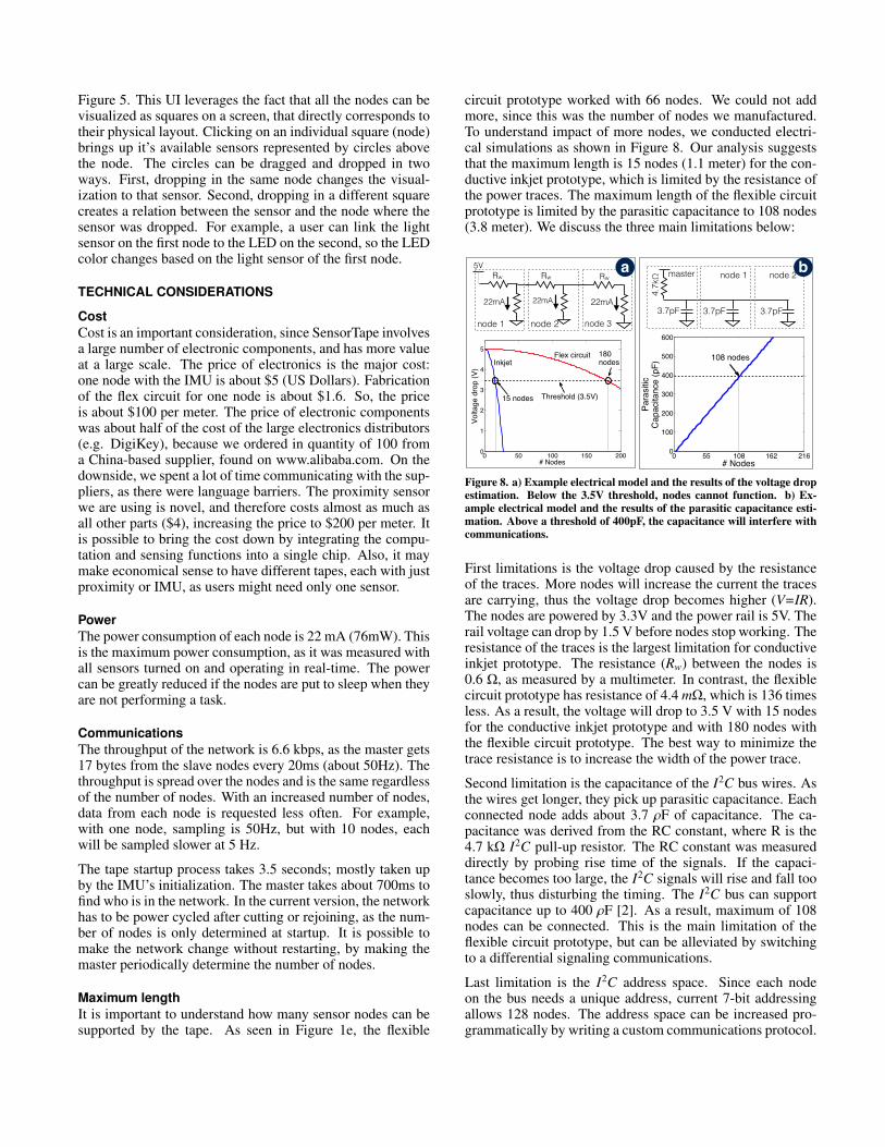
Figure 5. This UI leverages the fact that all the nodes can bevisualized as squares on a screen, that directly corresponds totheir physical layout. Clicking on an individual square (node)brings up it’s available sensors represented by circles abovethe node. The circles can be dragged and dropped in twoways. First, dropping in the same node changes the visual-ization to that sensor. Second, dropping in a different squarecreates a relation between the sensor and the node where thesensor was dropped. For example, a user can link the lightsensor on the first node to the LED on the second, so the LEDcolor changes based on the light sensor of the first node.
TECHNICAL CONSIDERATIONS
CostCost is an important consideration, since SensorTape involvesa large number of electronic components, and has more valueat a large scale. The price of electronics is the major cost:one node with the IMU is about $5 (US Dollars). Fabricationof the flex circuit for one node is about $1.6. So, the priceis about $100 per meter. The price of electronic componentswas about half of the cost of the large electronics distributors(e.g. DigiKey), because we ordered in quantity of 100 froma China-based supplier, found on www.alibaba.com. On thedownside, we spent a lot of time communicating with the sup-pliers, as there were language barriers. The proximity sensorwe are using is novel, and therefore costs almost as much asall other parts ($4), increasing the price to $200 per meter. Itis possible to bring the cost down by integrating the compu-tation and sensing functions into a single chip. Also, it maymake economical sense to have different tapes, each with justproximity or IMU, as users might need only one sensor.
PowerThe power consumption of each node is 22 mA (76mW). Thisis the maximum power consumption, as it was measured withall sensors turned on and operating in real-time. The powercan be greatly reduced if the nodes are put to sleep when theyare not performing a task.
CommunicationsThe throughput of the network is 6.6 kbps, as the master gets17 bytes from the slave nodes every 20ms (about 50Hz). Thethroughput is spread over the nodes and is the same regardlessof the number of nodes. With an increased number of nodes,data from each node is requested less often. For example,with one node, sampling is 50Hz, but with 10 nodes, eachwill be sampled slower at 5 Hz.
The tape startup process takes 3.5 seconds; mostly taken upby the IMU’s initialization. The master takes about 700ms tofind who is in the network. In the current version, the networkhas to be power cycled after cutting or rejoining, as the num-ber of nodes is only determined at startup. It is possible tomake the network change without restarting, by making themaster periodically determine the number of nodes.
Maximum lengthIt is important to understand how many sensor nodes can besupported by the tape. As seen in Figure 1e, the flexible
circuit prototype worked with 66 nodes. We could not addmore, since this was the number of nodes we manufactured.To understand impact of more nodes, we conducted electri-cal simulations as shown in Figure 8. Our analysis suggeststhat the maximum length is 15 nodes (1.1 meter) for the con-ductive inkjet prototype, which is limited by the resistance ofthe power traces. The maximum length of the flexible circuitprototype is limited by the parasitic capacitance to 108 nodes(3.8 meter). We discuss the three main limitations below:
node 1
Rw
22mA
0 50 100 150 2000
1
2
3
4
5
# NodesVo
ltage
dro
p (V
)
15 nodes Threshold (3.5V)
Flex circuitInkjet
180 nodes
Rw
22mA
Rw
22mA
node 2 node 33.7pF
0 55 108 162 2160
100
200
300
400
500
600
# Nodes
Para
sitic
Cap
acita
nce
(pF)
108 nodes
master
4.7k
Ω node 1 node 2
3.7pF3.7pF
a b5V
Figure 8. a) Example electrical model and the results of the voltage dropestimation. Below the 3.5V threshold, nodes cannot function. b) Ex-ample electrical model and the results of the parasitic capacitance esti-mation. Above a threshold of 400pF, the capacitance will interfere withcommunications.
First limitations is the voltage drop caused by the resistanceof the traces. More nodes will increase the current the tracesare carrying, thus the voltage drop becomes higher (V=IR).The nodes are powered by 3.3V and the power rail is 5V. Therail voltage can drop by 1.5 V before nodes stop working. Theresistance of the traces is the largest limitation for conductiveinkjet prototype. The resistance (Rw) between the nodes is0.6 ⌦, as measured by a multimeter. In contrast, the flexiblecircuit prototype has resistance of 4.4 m⌦, which is 136 timesless. As a result, the voltage will drop to 3.5 V with 15 nodesfor the conductive inkjet prototype and with 180 nodes withthe flexible circuit prototype. The best way to minimize thetrace resistance is to increase the width of the power trace.
Second limitation is the capacitance of the I2C bus wires. Asthe wires get longer, they pick up parasitic capacitance. Eachconnected node adds about 3.7 ⇢F of capacitance. The ca-pacitance was derived from the RC constant, where R is the4.7 k⌦ I2C pull-up resistor. The RC constant was measureddirectly by probing rise time of the signals. If the capaci-tance becomes too large, the I2C signals will rise and fall tooslowly, thus disturbing the timing. The I2C bus can supportcapacitance up to 400 ⇢F [2]. As a result, maximum of 108nodes can be connected. This is the main limitation of theflexible circuit prototype, but can be alleviated by switchingto a differential signaling communications.
Last limitation is the I2C address space. Since each nodeon the bus needs a unique address, current 7-bit addressingallows 128 nodes. The address space can be increased pro-grammatically by writing a custom communications protocol.
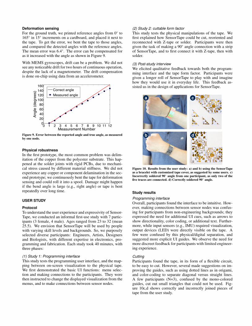
Deformation sensingFor the ground truth, we printed reference angles from 0� to165� in 15� increments on a cardboard, and placed it next tothe tape. To get the error, we bent the tape to those angles,and compared the detected angles with the reference angles.The mean error was 6.4�. The error can be compensated foras it increased with the angle as shown in Figure 9.
With MEMS gyroscopes, drift can be a problem. We did notsee any noticeable drift for two hours of continuous operation,despite the lack of a magnetometer. The drift compensationis done on-chip using data from an accelerometer.
0 1 2 3 4 5 6 7 8 9 10 11 12020406080
100120140160
Measurement Number
Angl
e (d
egre
es)
Correct angleMeasured angle
Figure 9. Error between the reported angle and true angle, as measuredby one node.
Physical robustnessIn the first prototype, the most common problem was delim-itation of the copper from the polyester substrate. This hap-pened at the solder joints with rigid PCBs, due to mechani-cal stress caused by different material stiffness. We did notexperience any copper or component delamination in the sec-ond prototype; we continuously bent the tape for deformationsensing and could roll it into a spool. Damage might happenif the bend angle is large (e.g., right angle) or tape is bentrepeatedly over long time.
USER STUDY
ProtocolTo understand the user experience and expressivity of Sensor-Tape, we conducted an informal first-use study with 7 partic-ipants (3 female, 4 male). Ages ranged from 23 to 32 (mean25.5). We envision that SensorTape will be used by peoplewith varying skill levels and backgrounds. So, we purposelyselected diverse participants: Engineers, Artists, Designersand Biologists, with different expertise in electronics, pro-gramming and fabrication. Each study took 40 minutes, withthree phases:
(1) Study 1: Programming interface
This study tests the programming user interface, and the map-ping between on-screen visualization to the physical tape.We first demonstrated the basic UI functions: menu selec-tion and making connections to the participants. They werethen instructed to change the displayed visualization from themenus, and to make connections between sensor nodes.
(2) Study 2: cuttable form factor
This study tests the physical manipulations of the tape. Wefirst explained how SensorTape could be cut, reoriented andreconnected with Z-tape or solder. Participants were thengiven the task of making a 90� angle connection with a stripof SensorTape, and to first connect it with Z-tape, then withsolder.
(3) Post-study interview
We elicited qualitative feedback towards both the program-ming interface and the tape form factor. Participants weregiven a longer roll of SensorTape to play with and imaginehow they would use it in everyday life. This feedback as-sisted us in the design of applications for SensorTape.
a
b
c
d
Figure 10. Results from the user study: a) and b) using the SensorTapeas a bracelet with customized tape cover, as suggested by some users. c)Incorrectly soldered 90� angle from one participant, as only two of thefive traces are connected. d) Correctly soldered 90� angle.
Study resultsProgramming interface
Overall, participants found the interface to be intuitive. How-ever, making connections between sensor nodes was confus-ing for participants from non-engineering backgrounds; theyexpressed the need for additional UI cues, such as arrows toshow directionality, color coding, or additional text. Further-more, while input sensors (e.g., IMU) required visualization,output devices (LED) were directly visible on the tape. Afew were confused by this physical/digital separation, andsuggested more explicit UI guides. We observe the need formore discreet feedback for participants with limited engineer-ing experience.
Cutting
Participants found the tape, in its form of a flexible circuit,to be easy to cut. However, several made suggestions on im-proving the guides, such as using dotted lines as in origami,and color-coding to separate diagonal versus straight lines.A few participants (N=3), confused by the mono-coloredguides, cut out small triangles that could not be used. Fig-ure 10c,d shows correctly and incorrectly joined pieces oftape from the user study.

Reconnecting
Participants were instructed to first reconnect SensorTapewith the Z-tape, then to remove the Z-tape and reconnect bysoldering. In general, participants found Z-tape to be easy touse, yet were concerned about flimsy connections. Almostall participants (N=6) had trouble understanding how Z-tapeworked, using it as they would normal tape. Soldering re-sulted in secure connections, yet it was time consuming, andespecially challenging for participants from non-engineeringbackgrounds. One participant suggested replacing the padswith holes, and using wire or conductive thread to tie theholes together to enable different angles. Others suggesteda standalone connector tape module, or tiny, conductive alli-gator clips for connection. We observe the need for a robustreconnection method that is accessible to participants fromvarious backgrounds.
Form factor
Many participants compared the form factor of SensorTape toa ribbon. They preferred a width of half an inch, comparableto that of tapes and ribbons used in arts and crafts.
Applications
Participants wanted to use SensorTape for an array of wear-able applications, such as sports and injury monitoring, ges-ture tracking, and bio-sensing. The wrist and arm were themost popular locations, as they are easily accessible and af-fords various gestures. Beyond miniaturizing the tape, sev-eral (N=4) participants wanted to personalize the appearanceof SensorTape by attaching a cover layer. This can be eas-ily done by attaching a layer of fabric, or colored maskingtape on the SensorTape surface. Some of the suggestions areshown in Figure 10a,b. Other suggested applications includeinventory tracking, home activity sensing, etc.
APPLICATION SCENARIOSIn each application scenario we will highlight two or morecore properties of SensorTape: cutting and joining two tapesstraight and at 90� angles, bending, and sensing shape andproximity. Applications emphasize low deployment effortthat can be achieved by the end user. Applications did notrequire any hardware modifications except cutting and join-ing, and did not need any node firmware changes. The appli-cations only required programming visualizations on the PC;the basic functions such as finding and updating the nodeswas done automatically.
Shape-measuring tool. Core properties explored: joining,bending, and shape sensing. In this application, SensorTapeis used to digitize curves of physical objects. Tape can bemade longer or shorter with minimum effort to enable a cus-tom shape-measuring tool. As shown in Figure 11, we use asmall six-node piece of tape to measure radius of a glass bot-tle; radius is estimated from the tape’s curvature. The smallpiece of tape is too short to record the profile of the bottle.Adding six more nodes enabled the user to capture the pro-file of the bottle. This requires little time, and no program-ming as the new piece is automatically added to the 3D sur-face. This high-dimensional input tool is similar in spirit to
ShapeTape [6] and HandSCAPE [16], but offers more cus-tomization. The 3D surfaces are controlled directly by mov-ing control points of a NURBS surface in OpenGL.
Wearable for posture monitoring. Core properties ex-plored: cutting, bending, and shape sensing. In this applica-tion we use deformation sensing algorithms to monitor pos-ture. Sensing is done by a piece of tape attached to the user’sback. The tape is powered by a battery and data is sent tothe phone over Bluetooth to alert if the user has bad posture.Because of flexibility issues, most modular electronics plat-forms are not comfortable to be used as wearable devices.SensorTape is flexible, and it can be cut to the right size tobe comfortably worn by the user. SensorTape allows quickprototyping and deployment of wearable sensors. As shownin Figure 11, setup step only involves cutting a roll of Sensor-Tape to custom clothing. By placing separate pieces of tapeon the arms, legs, and torso, it is possible to do body motiontracking.
Figure 11. Applications using self-sensing. Top: SensorTape can be at-tached to a clothing and tailored to custom length. Attached to the back,the tape is used to monitor posture. Bottom: the tape is used as a custom3D ruler. A smaller piece of tape is used to measure the diameter of aglass bottle, and a larger piece can measure the profile of the bottle.
Height measurement. Core properties: cutting and prox-imity sensing. We attached SensorTape vertically to the wallto measure the height of the person standing next to it. It isnot currently possible to digitally measure height without abulky and expensive height gage. Furthermore, it is not pos-sible to easily customize the size and shape of such gages.We used proximity sensors, and interpolated the informationfrom neighboring sensors to obtain 1 cm resolution. Lineararrays of sensors are well suited for height and displacementmeasurements, but are hard to implement quickly using cur-rent discrete electronics platforms. Implementing this appli-cation with the SensorTape took under 1 hour. Physical setuprequired only unrolling and cutting the a roll of SensorTape toa custom wall size. This application can be extended to manyhome sensing applications for presence/movement detection.

Interactive surface. Core properties: joining at 90� andproximity sensing. We created a coarse proximity-basedtouch screen by placing SensorTape around the edges of arectangular screen. A cursor on the screen can be controlledby simultaneously hovering the hands over horizontal andvertical edges. The size of the cursor can be controlled by theheight of the hands. The rectangular tape was created by cut-ting and jointing the segments at 90� angles. The deploymenteffort is significantly lower than that of prior proximity-awaretouch screen tables [5]. With SensorTape no firmware modifi-cations or hardware wiring was required, and the touchscreenUI was built fully in high-level Java. SensorTape allows quickprototyping of complex user interfaces with sensor arrays.
Figure 12. Applications using proximity sensing. Left: SensorTape isattached to the wall for height sensing. The proximity sensors can esti-mate the height of the person standing next to the tape. Right: by usingproximity sensors, a cursor can be controlled by hovering hands overhorizontal and vertical edges.
LIMITATIONS AND FUTURE WORKCommunications: I2C is designed for short distances, lim-iting the maximum length and the speed. Also, I2C canstop working when the signal wires are touched, as humanshave large capacitance. In the future we plan to use a dif-ferential signaling protocol, such as RS-485. This can beaccomplished by using a serial to RS-485 converter such asMAX481 (Maxim) at each node. Differential signals are ro-bust to parasitic capacitance, and allow for greater data rates.
The communications are not fully protected against node fail-ures; the peer-to-peer network requires each node to be oper-ational. The address assignment will fail for all nodes down-stream of the broken node. In future work, we will create aprotocol that combines a global I2C bus and a local P2P net-work to bypass broken nodes. By assigning a random addressat the start, the master can talk to nodes beyond a broken link.
Programming: For the platform to become more customiz-able, programming will need to be simplified on multiplelevels. Currently the firmware on slave nodes is loaded bydirectly connecting a programmer. If the user updates thefirmware, this can take a long time, as the number of slavescan be large. In the future we plan to write a bootloader thatcan load the software through the I2C bus.
If someone attempts to make their own version of the tape,it might take a lot of effort to write firmware for new digitalsensors. Nodes are not running an operating system, so thecore functionality is not abstracted from the sensors. Sincethe sensor nodes are driven by interrupts from the master andthe sensors, a simple event-driven node operating system willgreatly simplify development.
Usability: In the future work we will create a more intuitiveinterface. We found from the user study that both the UI andthe physical tape caused some confusion. Specifically, in theUI the participants found linking the sensors to be confusing.In the future we will label the inputs and the outputs clearly byarrows, and display the type of relationship. In the physicaltape, the cut lines were not clear, so many participants cut outsmall rectangles, making the tape hard to connect. We willprovide more visual cues such as colored lines and text, so theusers only cut diagonal and vertical lines. Many participantsfound it hard to reconnect the tape because solder pads are toosmall. In the future, we will increase the size of the pads andreduce their number from 5 to 4. The peer-to-peer line canbe removed by switching one of the bus wires as peer-to-peerduring initialization.
We only conducted limited user testing of the tape. To gaina greater understanding of advantages and disadvantages ofSensorTape, a larger workshop-based evaluation is required.To do so, we will need to make more pieces of tape, andstreamline the manufacturing process. Also, we released de-sign files at github.com/ResEnv, so the users can modify andbuild their own versions.
CONCLUSIONIn this work we presented SensorTape, a sensor network ona tape. It allows users to intuitively create and program largesensor network arrays. This will enable applications, that arenot possible with the current discrete electronics platforms.As with normal tape, SensorTape is flexible and cuttable, as itis made from flexible electronics. The SensorTape can be cutand rejoined to form a linear or a 2D surface. Furthermore, itis modular, as SensorTapes with different functionalities canbe joined together. We developed the network architecturethat automatically determines the length of the tape and thelocations of all sensors. We developed algorithms to do thetape’s surface reconstructing using IMUs, enabling a multi-tude of motion-related applications.
We demonstrated that it is feasible to manufacture Sensor-Tape using existing conductive inkjet and flexible electronicstechnologies. We show applications that leverage the uniquetape form factor. Since it is flexible, it can be comfortablyused for wearable applications, for example we attached it tothe back to monitor posture. The SensorTape can be used ashigh-dimensional input, such as tangible 3D curve manipula-tion. Furthermore, it can make a surface interactive, such asmaking a wall that can measure height or making a proximity-based touchscreen. To enable more custom applications wedeveloped an interface to graphically program the tape.
In the user study, we found that most participants saw the Sen-sorTape as a wearable device, that is easy to customize. Thiswas unexpected, since we originally envisioned it as some-thing that is placed on objects or in the environment. Further-more, the users suggested that SensorTape feels like materialfor arts and crafts, as it can be changed by cutting and joining.We believe that this project provides groundwork for futurematerials, which are very technologically sophisticated, andyet can be manipulated as a traditional tape or fabric.

ACKNOWLEDGMENTSThis project is partially supported by National Science Foun-dation award 1256082. We thank Nan-Wei Gong, FelixHeibeck, Nan Zhao for help and advice.
REFERENCES1. Conductive ink jet.
http://www.conductiveinkjet.com/.2. i2c-bus specifications. http://www.nxp.com/
documents/user_manual/UM10204.pdf, 2014.3. Seeduino film.
http://www.seeedstudio.com/wiki/Seeeduino_Film,2014.
4. Adafruit neopixel digital rgb led strip.http://www.adafruit.com/products/1138, 2015.
5. Annett, M., Grossman, T., Wigdor, D., and Fitzmaurice,G. Medusa: a proximity-aware multi-touch tabletop. InProc. of UIST, ACM (2011), 337–346.
6. Balakrishnan, R., Fitzmaurice, G., Kurtenbach, G., andSingh, K. Exploring interactive curve and surfacemanipulation using a bend and twist sensitive input strip.In Proc. of i3D, ACM (1999), 111–118.
7. Bdeir, A. Electronics as material: littlebits. In Proc. ofTEI, ACM (2009), 397–400.
8. Gong, N.-W., Hodges, S., and Paradiso, J. A. Leveragingconductive inkjet technology to build a scalable andversatile surface for ubiquitous sensing. In Proc. ofUbicomp, ACM (2011), 45–54.
9. Gong, N.-W., Steimle, J., Olberding, S., Hodges, S.,Gillian, N. E., Kawahara, Y., and Paradiso, J. A.Printsense: a versatile sensing technique to supportmultimodal flexible surface interaction. In Proc. of CHI,ACM (2014), 1407–1410.
10. Gong, N.-W., Wang, C.-Y., and Paradiso, J. A. Low-costsensor tape for environmental sensing based onroll-to-roll manufacturing process. In Proc. of Sensors,IEEE (2012).
11. Hill, J. L., and Culler, D. E. Mica: A wireless platformfor deeply embedded networks. Micro, IEEE 22, 6(2002), 12–24.
12. Holman, D., Fellion, N., and Vertegaal, R. Sensing touchusing resistive graphs. In Proc. of DIS, ACM (2014),195–198.
13. Kahn, J. M., Katz, R. H., and Pister, K. S. Next centurychallenges: mobile networking for smart dust. In Proc.of MobiCom, ACM (1999), 271–278.
14. Kawahara, Y., Hodges, S., Cook, B. S., Zhang, C., andAbowd, G. D. Instant inkjet circuits: lab-based inkjetprinting to support rapid prototyping of ubicompdevices. In Proc. of Ubicomp, ACM (2013), 363–372.
15. Lahey, B., Girouard, A., Burleson, W., and Vertegaal, R.Paperphone: understanding the use of bend gestures inmobile devices with flexible electronic paper displays.In Proc. of CHI, ACM (2011), 1303–1312.
16. Lee, J., Su, V., Ren, S., and Ishii, H. Handscape: avectorizing tape measure for on-site measuringapplications. In Proc. of CHI, ACM (2000), 137–144.
17. Lifton, J., Seetharam, D., Broxton, M., and Paradiso, J.Pushpin computing system overview: A platform fordistributed, embedded, ubiquitous sensor networks. InPervasive Computing. Springer, 2002, 139–151.
18. Merrill, D., Kalanithi, J., and Maes, P. Siftables: towardssensor network user interfaces. In Proc. of TEI, ACM(2007), 75–78.
19. Mistree, B. F., and Paradiso, J. A. Chainmail: aconfigurable multimodal lining to enable sensatesurfaces and interactive objects. In Proc. of TEI, ACM(2010), 65–72.
20. Olberding, S., Gong, N.-W., Tiab, J., Paradiso, J. A., andSteimle, J. A cuttable multi-touch sensor. In Proc. ofUIST, ACM (2013), 245–254.
21. Qi, J., and Buechley, L. Sketching in circuits: designingand building electronics on paper. In Proc. of CHI, ACM(2014), 1713–1722.
22. Rekimoto, J., Ullmer, B., and Oba, H. Datatiles: amodular platform for mixed physical and graphicalinteractions. In Proc. of CHI, ACM (2001), 269–276.
23. Rendl, C., Kim, D., Fanello, S., Parzer, P., Rhemann, C.,Taylor, J., Zirkl, M., Scheipl, G., Rothlander, T., Haller,M., et al. Flexsense: a transparent self-sensingdeformable surface. In Proc. of UIST, ACM (2014),129–138.
24. Richardson, B., Leydon, K., Fernstrom, M., andParadiso, J. A. Z-tiles: building blocks for modular,pressure-sensing floorspaces. In Proc. of CHI, ACM(2004), 1529–1532.
25. Vyas, R., Lakafosis, V., Lee, H., Shaker, G., Yang, L.,Orecchini, G., Traille, A., Tentzeris, M. M., and Roselli,L. Inkjet printed, self powered, wireless sensors forenvironmental, gas, and authentication-based sensing.Sensors Journal, IEEE 11, 12 (2011), 3139–3152.
26. Watanabe, R., Itoh, Y., Asai, M., Kitamura, Y., Kishino,F., and Kikuchi, H. The soul of activecube:implementing a flexible, multimodal, three-dimensionalspatial tangible interface. Proc. of CIE 2, 4 (2004),15–15.