senior project report - final (1) - cal poly
TRANSCRIPT

Electrical Engineering Department
California Polytechnic State University
Senior Project Final Report
MISO DC-DC Farmbot
June 10, 2020
Authors
Astha Adhikari
Brian Armijo
Quyen Nguyen
Advisors
Taufik
1
Contents
List of Figures 2
List of Tables 3
Acknowledgements 4
Abstract 4
Chapter 1. Introduction 5
Chapter 2. Background 10
Chapter 3. Design Requirements 12
Chapter 4. Design 16 Design Calculations 17
Chapter 5. Simulation Results and Analysis 25 Simulation Tool Selection 255 Simulation Setup 255 Simulation Results 29
Basic Controller 30 Turbine and Solar Input Equivalents 32 Parallel Controllers 33 Non-Ideal Components with Input and Output Filters 35 Full Functionality 36
Data Analysis 39
Chapter 6. Conclusion 41
References 43
A. Final Schematic 44
B. Project Schedule 45
C. Bill of Materials 46
D. Analysis of Senior Project Design 48

2
List of Figures
Figure 1.1: Power electronics technologies integration in renewable energy system 8 Figure 3.1: Current architecture of overall system provided by client 12 Figure 3.2: Level 0 block diagram of converter 13 Figure 3.3: Level 1 block diagram 133 Figure 4.1: Level 2 block diagram 16 Figure 4.2: Schematic of LT8705A controller and surrounding components 177 Figure 4.3: RSENSE graph and equations. 19 Figure 4.4: Input Capacitance vs Input Voltage 23 Figure 5.1: Basic controller simulation set up for measuring output voltage at 5A load. 266 Figure 5.2: Wind turbine input equivalent circuit, IV curve, and power curve 277 Figure 5.3: Solar panel input equivalent circuit, IV curve, power curve, and Is calculation Error! Bookmark not defined.7 Figure 5.4: Circuit and frequency response to find input filter inductor and capacitor values. 288 Figure 5.5: Input and output filter schematic 288 Figure 5.6: Full functionality simulation set up 29 Figure 5.7: Steady state output voltage and input current waveforms of basic circuit at 10V input and 5A load 30 Figure 5.8: Input and output power waveforms of basic circuit at 10V input and 5A load. 30 Figure 5.9: Output voltage waveforms at 0.5A and 5A loads. 31 Figure 5.10: Output voltage waveform at minimum, nominal, and maximum input voltage with 5A load. 311 Figure 5.11: FFT of steady state input current of basic circuit at 10V input and 5A load. 322 Figure 5.12: Input voltage, output voltage, and input current of turbine equivalent 333 Figure 5.13: Input voltage, output voltage, and input current of solar equivalent 333 Figure 5.14: Parallel controller output voltages before diodes and output diode currents 344 Figure 5.15: Parallel controller total output voltage and input currents of ideal parallel controllers 344 Figure 5.16: Parallel controller steady state input current FFT of 10V source 355 Figure 5.17: Parallel controller steady state input current FFT of 70V source 355 Figure 5.18: Output voltage and input current of controller with non-ideal filters 366 Figure 5.19: Steady state input current FFT of controller with non-ideal filters 366 Figure 5.20: Output voltages and diode currents of Full Circuit 377 Figure 5.21: Output voltages before and after diodes of Full Circuit Error! Bookmark not defined.7 Figure 5.22: Input voltages and currents of Full Circuit 38 Figure 5.23: Steady state turbine input current FFT of Full Circuit 38 Figure 5.24: Steady state solar input current FFT of Full Circuit 39

3
List of Tables
Table 3.1: Design requirements and justification 14 Table 5.1: Summary of Simulation Results 39

4
Acknowledgements
We would like to thank our advisor Dr. Taufik for his passion and knowledge of power electronics. This
project has opened doors into applying our shared knowledge of this subject. We are thankful for his
guidance in completing this project during this unprecedented time. We would also like to extend our
appreciation to Chris Arntzen, our client for his active participation on the project. Finally, we would like
to thank the Cal Poly EE department and our friends and family for all their support.

5
Abstract
Making use of renewable energy directly from the location of production requires converting source
power into usable power. The specific scope of this project focuses on the DC to DC conversion within a
user friendly universal farmbot system. Since renewable sources vary widely in voltage and current, a
wide input-range DC to DC converter is desired. Physical isolation, long lifespan, and adverse weather
requires safe and reliable final product specifications. The goal of a very wide customer base drives the
need for a product that does not require tinkering to get working, but to be usable out of the box for a vast
majority of energy sources. This project designs, purely through simulation due to COVID-19 pandemic,
a Universal Input Module (UIM) DC-DC converter, which acts as the first step from the energy source to
the usable power bus. UIMs can be connected in parallel to effectively make a Multiple Input Single
Output (MISO) system. The main component of conversion is a 4-switch buck-boost controller. Input
filtering, output filtering, parallel function, and two theoretical renewable inputs are incorporated to give
the simulated converter as realistic of a function as possible. The selection process for all main
components, surrounding components, and equivalent simulation circuits is included. With use of
LTSpice, the simulation results meet the customer’s specifications.

6
Chapter 1. Introduction
Electrical power can change in wattage, voltage, current, frequency, DC vs AC, phase count, and
power factor. The most efficient form of generation, transmission, and use of power varies from
application to application. For example, while most generation and transmission use AC power, many
consumer products require DC power, which requires a device that converts AC voltage to DC voltage
efficiently, generally known as rectifier [1]. The enabling technology that provides such an efficient
conversion from one form of electrical power to another is known as power electronics.
Historically speaking, the defining goal of power electronics followed the same principle as it
does today: maximizing financial efficiency. While early prototypes of electric generation and use
required little to no transmission, the first step to a commercially available power grid in 1882 proved
tough as the 57 km line, from the Bavarian Alps to Munich, came in at around 50% transmission
efficiency. The first form of generation and distribution of electrical power was even worse as the first 80
customers ever served, on Pearl Street Manhattan, were supplied by six dynamos with 6% overall
efficiency. These DC generators and lines sufficiently supplied short distance grids at low DC voltage
level but were soon out-competed by high-voltage AC as line and transformer loss decreased with the
higher voltages [2]. By 1902 a single power station, designed by Nikola Tesla and established by George
Westinghouse, supplied an 11 kV three-phase AC line across 32km to Buffalo, producing a fifth of
electricity in the United States [3]. Business was driving the need for more and more efficient forms of
power use and there only seemed to be ever increasing opportunities for budding technology to play a
role.
Power electronics of today follows the use of semiconductor devices as tools in increasing input
to output power efficiency. The component categories fall under their association to AC and DC power:
rectifier for AC to DC conversion, inverters for DC to AC conversion, DC-DC converters, and AC-AC
converters. Efficiency depends on three areas of possible improvement: smarter real-time control of
devices, device topology, and device technology [1]. For example, both a snubber circuit, a topology, and

7
higher quality MOSFETs can reduce switching losses, but the correct choice depends on the exact
application at hand. As a secondary priority among businesses emerges, the environmental impacts of
industry, power electronics asks the question of how to reduce emissions. Since renewable is the
empowering answer among small scale investors, the change in power generation demands different
forms of electrical conversion.
The main advantages of using renewable energy sources is that it is sustainable and low in
pollution. Fossil fuels are finite resources that cannot be used indefinitely and cause pollution during
combustion. Renewable energy such as solar, wind, hydropower, geothermal, solar photovoltaic etc.
offers better environmental and economic benefits as they produce no greenhouse gases. As a result, there
has been a significant demand for renewable resources in recent years. Countries like Denmark expect to
be 100% fossil-free by 2050 [4]. With the shift in the energy paradigm from fossil-based resources to
renewables in the past decades, power electronics has become more popular in increasing efficiency for
renewable energy sources. The most emerging renewable energy sources (wind and photovoltaic) make
use of power electronics technology in generation, grid integration, transmission, and end-user
application. Figure 1.1 summarizes the broad picture of how power electronics is used to implement
renewable sources. In this figure the power electronics block converts the DC output voltage from the
renewable energy source such as solar panels to AC voltage which can be used directly by the load as
well as fed back to the grid. For wind generators, power electronics may be used to regulate the varying
AC output voltage due to the varying wind speed to the AC output voltage required by the load or grid.
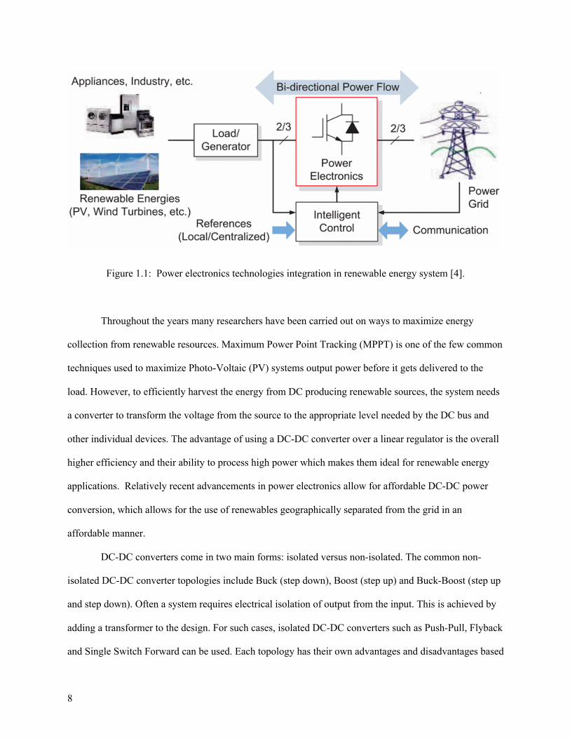
8
Figure 1.1: Power electronics technologies integration in renewable energy system [4].
Throughout the years many researchers have been carried out on ways to maximize energy
collection from renewable resources. Maximum Power Point Tracking (MPPT) is one of the few common
techniques used to maximize Photo-Voltaic (PV) systems output power before it gets delivered to the
load. However, to efficiently harvest the energy from DC producing renewable sources, the system needs
a converter to transform the voltage from the source to the appropriate level needed by the DC bus and
other individual devices. The advantage of using a DC-DC converter over a linear regulator is the overall
higher efficiency and their ability to process high power which makes them ideal for renewable energy
applications. Relatively recent advancements in power electronics allow for affordable DC-DC power
conversion, which allows for the use of renewables geographically separated from the grid in an
affordable manner.
DC-DC converters come in two main forms: isolated versus non-isolated. The common non-
isolated DC-DC converter topologies include Buck (step down), Boost (step up) and Buck-Boost (step up
and step down). Often a system requires electrical isolation of output from the input. This is achieved by
adding a transformer to the design. For such cases, isolated DC-DC converters such as Push-Pull, Flyback
and Single Switch Forward can be used. Each topology has their own advantages and disadvantages based

9
on application. There are other topologies that further improve upon these designs by reducing switching
losses with the use of soft switching techniques. The type of converter used depends on the design
metrics, but there are always tradeoffs between cost, board space and efficiency.
One unique application of DC-DC converters calls for a way to combine multiple energy sources
to power a single DC bus. Such a converter is called Multiple Input Single Output (MISO) DC-DC
converter. In [5], [6], and [7], multiple well-known DC-DC topologies have been studied to determine
which topology provides the most practical solution for the multiple input single output DC-DC
converter.

10
Chapter 2. Background
Renewables meet the energy and environmental demands of the public and private sector in an
economical way. Choices supporting sustainable options have ramped up over the past few decades,
already reaching $155 billion yearly spending a decade ago [8]. Recent business practices show conscious
decisions to purchase green power, both for morality and to improve “employee morale” [9]. Not all
renewables are the same though, as theoretical research is helping identify the most viable sustainability
options among those currently available on the market [10]. As the original investment to renewables is
relatively small, it proves to be a uniquely attractive option among private investors. Affordability among
an entire energy system looking to make use of renewable energies is paramount. Power conversion is
necessary to bridge the gap between the morally driven and practical business opportunity.
To make use of renewables requires electrical conversion accommodating for low electrical
inertia, physical isolation, and non-linear power production curves. Renewables generally do not follow
the traditional expectations of steady output power. As a remedy to highly variable production, most opt
to make use of multiple renewable energy sources at once, specifically wind and solar. Efficiently
sourcing from two or more renewables requires a wide input range and max power point tracking. A
viable system making use of renewable energy also requires batteries to provide “power balance,” even
when connected to the grid [11]. Within systems isolated from the public grid, commonly called
microgrids, the shortcomings of renewables become more apparent as no power alternatives exist.
Research into rural microgrid planning shows the deeply economic process of producing electricity in
physical isolation [12]. As is commonly concluded, the most economically viable option for physically
isolated renewable energy systems include the use of a two input, wide input range, and battery connected
DC-DC converter [13].
The type of DC-DC converter topology depends on the application of the overall circuit. Initial
MISO prototype [14] by students at California Polytechnic University uses a full bridge topology. In a
full bridge transformer, each input source uses a single primary winding thus minimizing the transformers
11
sizes. The overall circuit is also relatively small for the same output power compared to other isolated
topologies. Another senior project [15] improved on the original design’s efficiency and lack of isolation
by implementing a flyback converter instead of full bridge. A flyback converter uses only one switch and
one winding per input which reduces cost and complexity of the control circuit. On the non-isolated
converter side, a four switch buck boost design was implemented for a USB-Charger by another group of
students [16].The use of four switch buck boost gets rid of the negative polarity which is what one gets
from a traditional buck boost circuit. This circuit is relatively simple compared to the isolated converters.
As mentioned earlier, the type of DC-DC converter topology depends on the applications and
requirements. In cases where isolation of inputs and outputs are not needed, traditional non-isolated DC
converters such as buck, boost, or buck boost can be used. This project focuses on the DC-DC converter
application on a farmbot for a wide input range of 10V-80V from two renewable sources. Either a flyback
or buck-boost converter can be used for the design. After comparing previous designs with the customer's
recommendations, a simple OR diode configuration using four switch buck-boost converters is proposed
for this project. There are two ways to implement OR diodes in a MISO converter [17]. One way is to
connect each source to an energy source to an OR diode and use a converter. An alternative way is to
implement a converter on each source followed by an OR diode which connects to the load. This project
implements the second design to make equal use of all inputs by using a DC-DC converter per power
source.
The objective of this project is therefore to design and build a multiple input single output DC-
DC converter that will make use of two sources such as wind and solar. Each source will be interfaced as
an input to their corresponding MISO converter. The topology used within the MISO converter is the 4-
switch Buck-Boost topology. The output of these MISO converters is then combined to get a single DC
output voltage to provide energy sufficient for small-scale farming application. OR diode configuration
will be used to establish the common connection from each MISO converter. Hardware prototype of the
MISO converter will be designed, constructed, and tested to evaluate its performance. Cost analysis of the
converter will also be provided as part of the deliverables from this project.

12
Chapter 3. Design Requirements
The client for this project specifies the intended engineering specifications for the DC-DC
converter. The converter is part of a bigger system that the client is working on as shown in Figure 3.1.
This project focuses on the buck boost converter and the battery charging circuits. While the required
input range and steady output voltage is required, most other specifications are open to flexibility. The
design requires taking in two sources, or potentially more in the future with modular design, and
converting them in parallel to a steady output voltage line. The client also wants the product to act as a
reliable, long-lasting, somewhat universal DC-DC power converter.
Figure 3.1: Current architecture of overall system provided by client

13
Figure 3.2: Level 0 block diagram of converter
Figure 3.2 shows the system's performance from an outside perspective. As the target customer
will want a dependable power production as possible, the likely usage of this converter will take in
multiple inputs of varying types. Multiple input types will require a wide input voltage range. The basic
concept of power conversion will include a buck-boost topology such as the 4-switch buck-boost
converter whose output is set at 24V.
Figure 3.3: Level 1 block diagram
Figure 3.2 displays the proposed level 0 block diagram of the DC-DC converter. The solar and
wind sources will be simulated using power supplies. The battery system is made of Interstate DCM0035
14
35Ah battery. Maximum power point tracking (MPPT) boards will convert each input to the maximum
possible power. These will be in line with the 4-switch buck-boost converter which will be the driving
board for setting the output to 24V. The 4-switch buck boost should have input voltage ranging from 10V
to 70V which would be the range provided by the renewable energy sources. The 4-switch buck boost
converter will be chosen over the standard buck-boost due to the positive output-input transfer function
that it provides, unlike the negative output voltage given by the traditional buck boost circuit. A Buck
module with MPPT battery controller will also be used to maximize the output power delivered by the
energy sources. The diodes from each converter path combine the energy from the multiple renewable
energy sources to the single 24V DC output bus.
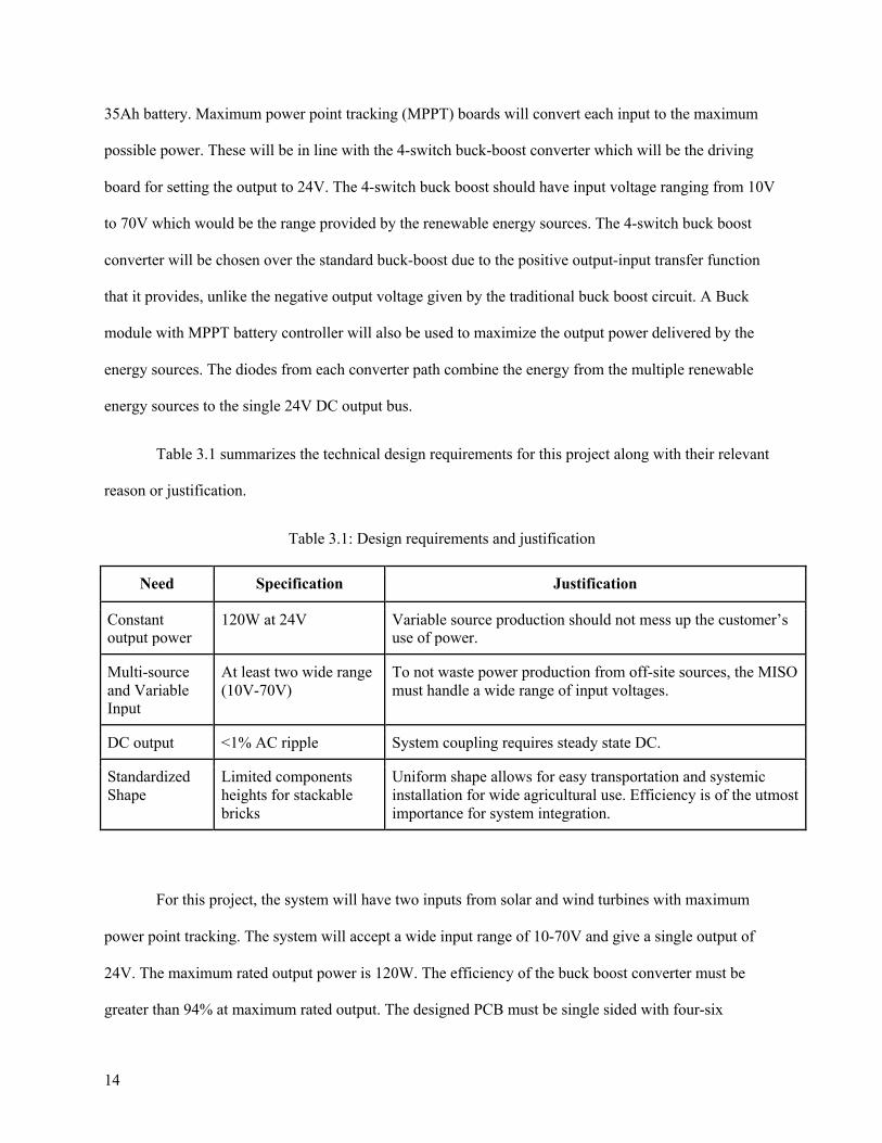
Table 3.1 summarizes the technical design requirements for this project along with their relevant
reason or justification.
Table 3.1: Design requirements and justification
Need Specification Justification
Constant output power
120W at 24V Variable source production should not mess up the customer’s use of power.
Multi-source and Variable Input
At least two wide range (10V-70V)
To not waste power production from off-site sources, the MISO must handle a wide range of input voltages.
DC output <1% AC ripple System coupling requires steady state DC.
Standardized Shape
Limited components heights for stackable bricks
Uniform shape allows for easy transportation and systemic installation for wide agricultural use. Efficiency is of the utmost importance for system integration.
For this project, the system will have two inputs from solar and wind turbines with maximum
power point tracking. The system will accept a wide input range of 10-70V and give a single output of
24V. The maximum rated output power is 120W. The efficiency of the buck boost converter must be
greater than 94% at maximum rated output. The designed PCB must be single sided with four-six

15
mounting holes. All component heights shall be limited to less than 1.25 inches. The PCB dimensions
must not exceed 3 inches by 5 inches to fit the existing platform. The module should cost less than $150
at a quantity of 100 modules. This includes electrical components, connectors, thermal interface materials
and PCB.
16
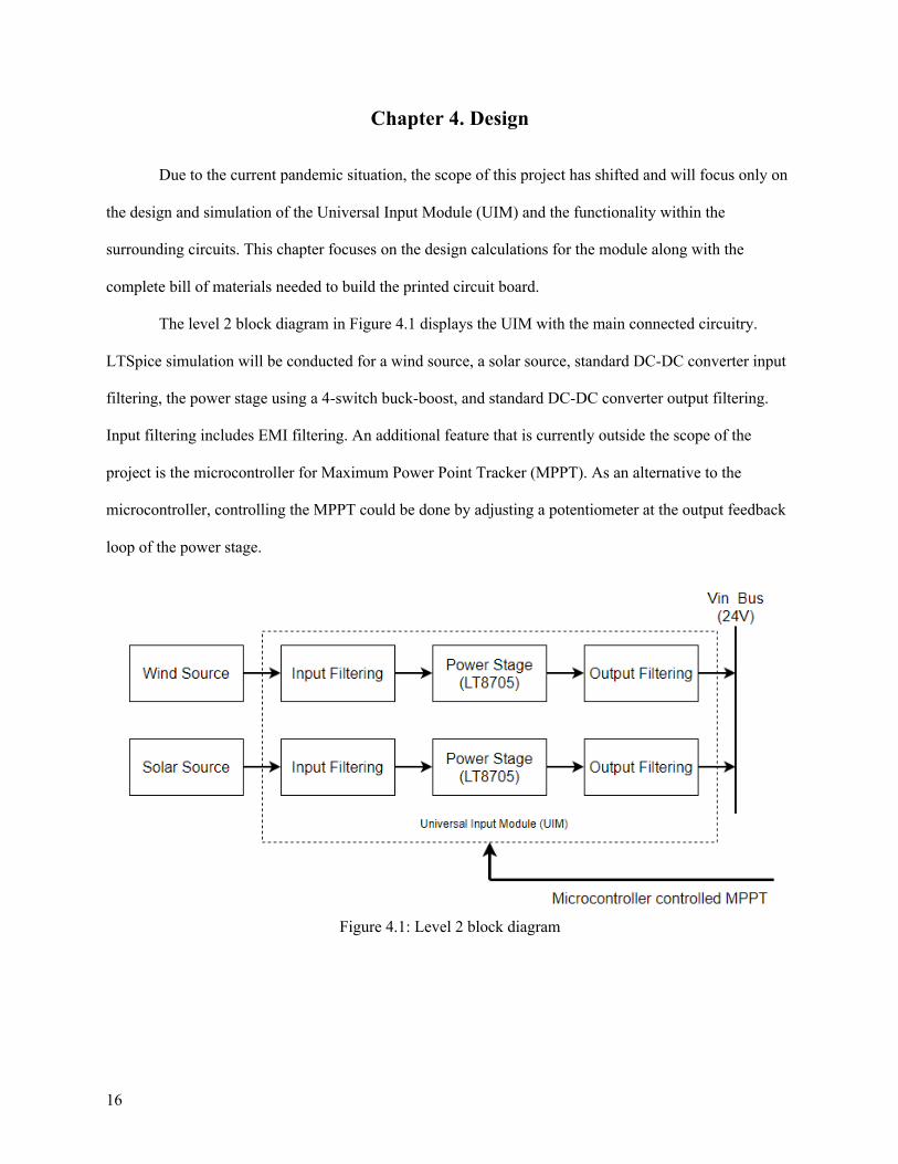
Chapter 4. Design
Due to the current pandemic situation, the scope of this project has shifted and will focus only on
the design and simulation of the Universal Input Module (UIM) and the functionality within the
surrounding circuits. This chapter focuses on the design calculations for the module along with the
complete bill of materials needed to build the printed circuit board.
The level 2 block diagram in Figure 4.1 displays the UIM with the main connected circuitry.
LTSpice simulation will be conducted for a wind source, a solar source, standard DC-DC converter input
filtering, the power stage using a 4-switch buck-boost, and standard DC-DC converter output filtering.
Input filtering includes EMI filtering. An additional feature that is currently outside the scope of the
project is the microcontroller for Maximum Power Point Tracker (MPPT). As an alternative to the
microcontroller, controlling the MPPT could be done by adjusting a potentiometer at the output feedback
loop of the power stage.
Figure 4.1: Level 2 block diagram

17
Figure 4.2: Schematic of LT8705A controller and surrounding components
Design Calculations
To perform the design calculations for the proposed system, we will need to have a set of operating
parameters. The following lists the provided parameter values:
Switching Frequency fsw
We specify a moderate switching frequency in given values but recalculate the frequency when
selecting a standard Rf value.
Peak to peak Inductor Current Ripple IL_ppmaxPerc
This is typically given in percentage of the maximum average inductor current. A range of 30%-
40% is the widely accepted industry normal range to start the design.
Peak to peak Input Voltage Ripple Vi_ppmaxPerc
18
This is also typically given in terms of maximum percentage of the actual average input voltage.
Percentage of 5% or less is quite common for power supplies.
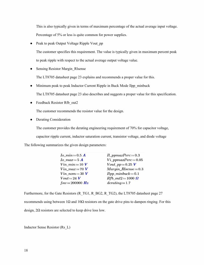
Peak to peak Output Voltage Ripple Vout_pp
The customer specifies this requirement. The value is typically given in maximum percent peak
to peak ripple with respect to the actual average output voltage value.
Sensing Resistor Margin_Rlsense
The LT8705 datasheet page 23 explains and recommends a proper value for this.
Minimum peak to peak Inductor Current Ripple in Buck Mode Ilpp_minbuck
The LT8705 datasheet page 23 also describes and suggests a proper value for this specification.
Feedback Resistor Rfb_out2
The customer recommends the resistor value for the design.
Derating Consideration
The customer provides the derating engineering requirement of 70% for capacitor voltage,
capacitor ripple current, inductor saturation current, transistor voltage, and diode voltage
The following summarizes the given design parameters:
Furthermore, for the Gate Resistors (R_TG1, R_BG2, R_TG2), the LT8705 datasheet page 27
recommends using between 1Ω and 10Ω resistors on the gate drive pins to dampen ringing. For this
design, 2Ω resistors are selected to keep drive loss low.
Inductor Sense Resistor (Rs_L)

19
Page 7 of the LT8705 datasheet provides a figure as replicated in Figure 4.3 to calculate the
maximum sense voltage in boost mode depending on the duty cycle. With a duty cycle of 58.3%
the maximum sense voltage is 9.8mV, which is used in later calculations.
“RSENSE Selection and Maximum Current” section in the LT8705 datasheet starts on page 22
and explains all required calculations. Inductor current ripple in Buck mode
ILrippleBUCKpercent and the MarginRsense are given as well in the same section.
The final value of 5mΩ was chosen for the RSENSE resistor.
Figure 4.3: RSENSE graph and equations.
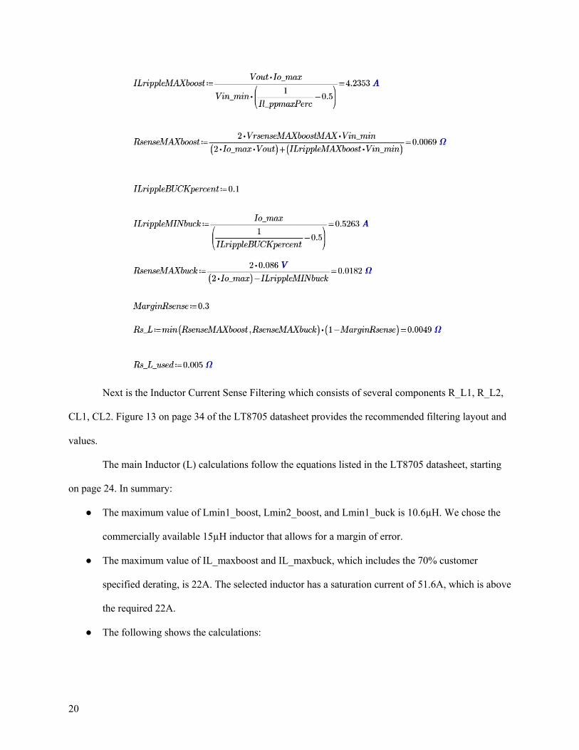
20
Next is the Inductor Current Sense Filtering which consists of several components R_L1, R_L2,
CL1, CL2. Figure 13 on page 34 of the LT8705 datasheet provides the recommended filtering layout and
values.
The main Inductor (L) calculations follow the equations listed in the LT8705 datasheet, starting
on page 24. In summary:
The maximum value of Lmin1_boost, Lmin2_boost, and Lmin1_buck is 10.6µH. We chose the
commercially available 15µH inductor that allows for a margin of error.
The maximum value of IL_maxboost and IL_maxbuck, which includes the 70% customer
specified derating, is 22A. The selected inductor has a saturation current of 51.6A, which is above
the required 22A.
The following shows the calculations:
21
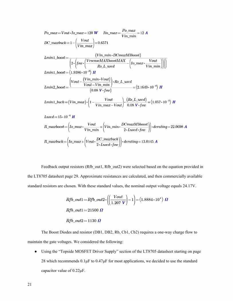
Feedback output resistors (Rfb_out1, Rfb_out2) were selected based on the equation provided in
the LT8705 datasheet page 29. Approximate resistances are calculated, and then commercially available
standard resistors are chosen. With these standard values, the nominal output voltage equals 24.17V.
The Boost Diodes and resistor (DB1, DB2, Rb, Cb1, Cb2) requires a one-way charge flow to
maintain the gate voltages. We considered the following:
Using the “Topside MOSFET Driver Supply” section of the LT8705 datasheet starting on page
28 which recommends 0.1μF to 0.47μF for most applications, we decided to use the standard
capacitor value of 0.22μF.

22
Additionally, page 29 of the same datasheet recommends a resistor up to 5Ω to be placed in series
with the diodes. The resistor reduces surge current on the diodes.
The next component is the Switch Enable Pullup Resistor (Rswen). This is a resistor that connects
the SWEN pin to the LDO pin to enable switching. The datasheet states that a commonly used resistance
for a pull-up resistance is 100kΩ.
Input voltage lockout resistors (Rlock_in1, Rlock_in2) are next to determine. These resistors
serve as a voltage divider for the shutdown pin, typically chosen as 33kΩ and 10kΩ resistors. These
values correspond to the controller shutting down and turning on at input voltages of 5.3V and 5.1V,
respectively. The resistor values must also be selected to fall under the maximum allowable SHDN pin
voltage. 33kΩ and 10kΩ set the allowable pin voltage between 2.33V to 16.3V, which is well within the
functional range of 1.234V and 30V.
Another component is the loop compensation (Rc, Cc1, Cc2). Page 33 of the datasheet includes a
brief paragraph on loop compensation. After simulation testing, the output voltage ripple performed best
at a resistor Rc of 20kΩ. The capacitor values did not adjust the output voltage ripple greatly; thus, the
recommended values are kept the same.
To set the switching frequency, the Frequency Controlling Resistor (Rt) needs to be chosen
properly. This is the resistor which is connected from the Rt pin to ground. We did the calculation for Rt
first, pick a standard Rt value next, and then recalculate the actual switching frequency. The following
shows the calculations.
23
Input Ripple Reduction Capacitor (Cin) is needed to reduce the peak to peak input voltage ripple.
Page 136 of the EE527 textbook provides the following equation. Plotting input capacitance vs. Input
voltage as shown in Figure 4.4 displays the peak input capacitance required at just over 3µF.
Figure 4.4: Input Capacitance vs Input Voltage
Peak to peak Output Voltage Ripple Reduction with Output Capacitor (Co1). Reducing output
voltage ripple requires capacitance to store bulk charge. Simulation of controller at worst performing
input, 10V in and 5A out, yielded an electrolytic minimum capacitance around 150µF. This was a higher
value than what the calculations yielded, as shown below to be 14µF.
24
Another needed capacitor is the Output Switching Spikes Reduction capacitor (Co2). Steady-state
output voltage contains ripples with switching spikes. A capacitor in parallel at a minimum of around
50µF yielded good transient steady state settling time in simulations.
Bypass Capacitors (Cvcc, C_LDO, Cvi) as described on page 32 of the LT8705 datasheet
requires a minimum of 4.7μF ceramic capacitance from INTVCC and GATEVCC to ground. Pages 11
and 12 list LDO33 and Vin pins as requiring bypass capacitors. The commonly used value of 1µF is used.
Next, the Soft-Start Capacitor (Css) is a capacitor connected from the SS pin to ground to control
the speed of voltage ramp on startup. While 5nF was used for faster simulations, page 15 of the LT8705
datasheet recommends a minimum of 100nF.
Lastly, switches (MT1, MB1, MB3, MT2) will be 4 MOSFET switches that are rated based on
minimum voltage and current ratings. Page 138 and 139 of the EE527 textbook list all the following
equations. Minimum and maximum duty cycles of 0 and 1 are used for worst case scenarios.
25
Chapter 5. Simulation Results and Analysis
Simulation Tool Selection
All simulations are done using LTspice. At no cost to users, LTspice allows free and easy use by
the current design team and all future engineers. Familiarity of the software among team members makes
the software the first choice among electronic simulations. The software also allows easy compatibility of
components, specifically the automatically included LT8705A controller, and gives confidence in the
credibility of the simulated results. In addition, it does not require subscription or payment which
contributes towards the goal of the project to be an open source project.
Simulation Setup
The first simulation includes a basic controller functionality circuit schematic. This is the
standard circuitry around the controller with a single input and output capacitor with an ideal input source
of range 10V to 70V and load ranging from 0.5A to 5A. This is included in the first level since the circuit
cannot function without bulk charge storage on input and output capacitors. No equivalent series
resistance (ESR) values are added during the ideal testing.

26
Figure 5.1: Basic controller simulation set up for measuring output voltage at 5A load.
The controller is designed to be in use with renewable energy sources, specifically wind turbine
and solar panel inputs. A wind turbine and solar panel equivalent circuit input voltage and current into the
controller. Each equivalent circuit is input to the controller and simulated separately.
Figure 5.2 and 5.3 show the design approach to each equivalent circuit. The calculation of Figure
5.3 is used with a guessed N value, usually 10-100, and then tested with a voltage source on the output.
The value of N is changed until the curve fits approximately a realistic PV solar panel IV curve. The
specific values are used to give realistic input sources for a 120W max output converter. Table 5.1, at the
end of this chapter, shows load currents at 3A and 1.5A for turbine and solar inputs, respectively. The low
load currents are necessary to allow production of enough power by the equivalent input circuits. If the

27
circuit wants to be tested at full load with solar and turbine inputs, then much larger solar and turbine
sources will need to be used.
Figure 5.2: Wind turbine input equivalent circuit, IV curve, and power curve
Figure 5.3: Solar panel input equivalent circuit, IV curve, power curve, and Is calculation
Realistic functionality requires taking in two or more sources at once. Controllers are diodes
connected together in parallel to accommodate multiple sources. For the first parallel simulation, the
inputs are ideal. The first input is 10V. The second input is delayed by 5ms and then takes 5ms to get up
to 70V. Testing a delayed input can show controllers function both separately and together. Figure 5.6 of
28
the fully functional circuit shares the same diode connections as the ideal parallel layout. The following
model is used as an equivalent of the SM74611KTTR low forward-voltage diode.
The filtering simulations are designed to help meet specifications while taking into account major
non-idealities. The engineering specifications require 250mV maximum peak to peak output voltage
ripple, and -40dB filtering of the input current. The input filter adds Li and Ci2 in parallel within the input
loop. Within Figure 5.4, the added 4.7µH inductor and 150nF capacitor add a notch at the switching
frequency of the controller. Simulation setup of the output filter adds Co2 within the output loop. Non-
ideal ESR values of 250mΩ for Ci, 1.6mΩ for Li, and 25mΩ for Co1 are added to the component
definitions.
Figure 5.4: Circuit and frequency response to find input filter inductor and capacitor values.
Figure 5.5: Input and output filter schematic

29
The final circuit is the full functionality circuit that employs all the specifications mentioned
above. It adds the basic circuit of Figure 5.1 with the filters of Figure 5.5, the input sources of Figure 5.2
and 5.3, in parallel with the diode model mentioned previously.
Figure 5.6: Full functionality simulation set up
Simulation Results
Tabulated results are summed up in Table 5.1 at the end of this chapter. The table includes input
voltage, output current, output voltage ripple, input current attenuation in dB, and efficiency all obtained
from the waveforms.

30
Basic Controller
The peak to peak output voltage ripple is 71.6mV at steady state. Under ideal conditions, the
basic circuit does not need any extra output filtering.
Figure 5.7: Steady state output voltage and input current waveforms of basic circuit at 10V input and
5A load
Figure 5.8: Input and output power waveforms of basic circuit at 10V input and 5A load.
Figure 5.8 shows input power oscillating greatly, even during steady state. Since input voltage is
constant, this equates to very high oscillations in input current. Output voltage and power rise as
expected.
31
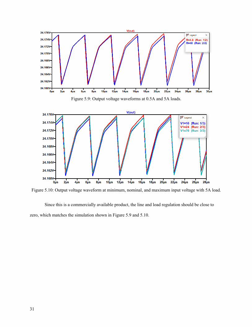
Figure 5.9: Output voltage waveforms at 0.5A and 5A loads.
Figure 5.10: Output voltage waveform at minimum, nominal, and maximum input voltage with 5A load.
Since this is a commercially available product, the line and load regulation should be close to
zero, which matches the simulation shown in Figure 5.9 and 5.10.

32
Figure 5.11: FFT of steady state input current of basic circuit at 10V input and 5A load.
With the ideal basic circuit, the frequency of the input current does not meet the desired -40dB
attenuation. The highest points correspond to switching frequency and harmonics of switching frequency.
-10dB is 30dB away from engineering specs, while many harmonics are also above.
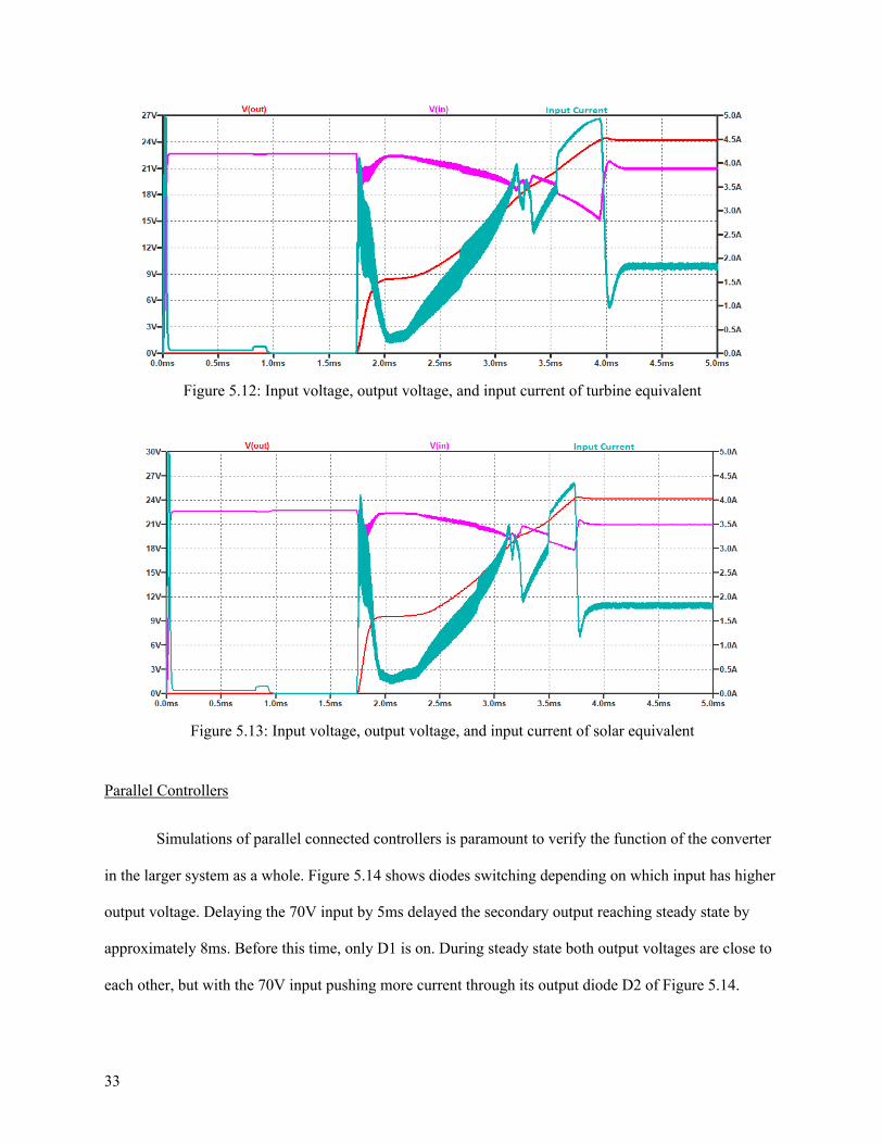
Turbine and Solar Input Equivalents
Since the equivalent sources are not tested at full load, many specs are not graphed or recorded.
Fluctuations of inputs approximately change inversely, which matches the equivalent curves of Figure 5.2
and 5.3. This simulation is mostly to verify the equivalent circuit functions as expected. Some other
values are in Table 5.1 at the end of this chapter.
33
Figure 5.12: Input voltage, output voltage, and input current of turbine equivalent
Figure 5.13: Input voltage, output voltage, and input current of solar equivalent
Parallel Controllers
Simulations of parallel connected controllers is paramount to verify the function of the converter
in the larger system as a whole. Figure 5.14 shows diodes switching depending on which input has higher
output voltage. Delaying the 70V input by 5ms delayed the secondary output reaching steady state by
approximately 8ms. Before this time, only D1 is on. During steady state both output voltages are close to
each other, but with the 70V input pushing more current through its output diode D2 of Figure 5.14.
34
Previously, the output diodes were not selected. Older simulations showed significant power loss
due to forward-voltage diode drop. The SM74611KTTR acts as a great option for a low forward-voltage
diode. The date sheet lists power loss at 8A to be 208mW. With lower output current and a non-linear
power loss curve, the expected power loss is about 100mW. Simulations yielded total diode power loss of
78mW. Either way, this allows for a much higher efficiency when controllers are connected in parallel.
Figure 5.14: Parallel controller output voltages before diodes and output diode currents
Figure 5.15: Parallel controller total output voltage and input currents of ideal parallel controllers
Figure 5.15 shows very high spikes, especially at steady state of the input current from the 70V
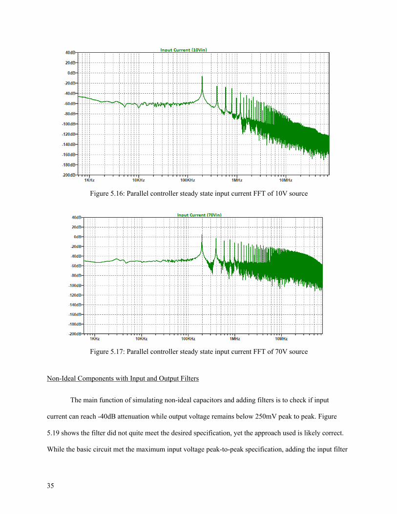
source. Without input filtering, parallel connected controllers do not meet EMI. Figures 5.16 and 5.17
show more clearly the frequency domain of the input current.
35
Figure 5.16: Parallel controller steady state input current FFT of 10V source
Figure 5.17: Parallel controller steady state input current FFT of 70V source
Non-Ideal Components with Input and Output Filters
The main function of simulating non-ideal capacitors and adding filters is to check if input
current can reach -40dB attenuation while output voltage remains below 250mV peak to peak. Figure
5.19 shows the filter did not quite meet the desired specification, yet the approach used is likely correct.
While the basic circuit met the maximum input voltage peak-to-peak specification, adding the input filter

36
increased it. Through simulation, minimum ceramic capacitance came out to be 50µF. Capacitance
greatly below would not meet the maximum output voltage ripple of 250mV. 47µF is used as a common
component value. Figure 5.18 displays the transient as well as low current and voltage ripple.
Figure 5.18: Output voltage and input current of controller with non-ideal filters
Figure 5.19: Steady state input current FFT of controller with non-ideal filters
Full Functionality
As seen in Figure 5.20, both output voltages rise very smoothly. Since both voltages are very
close to each other before the diodes, as seen in Figure 5.21, the diodes end up sharing the total output
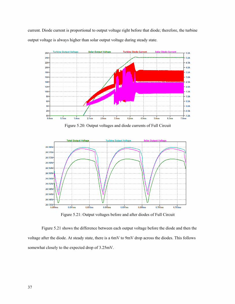
37
current. Diode current is proportional to output voltage right before that diode; therefore, the turbine
output voltage is always higher than solar output voltage during steady state.
Figure 5.20: Output voltages and diode currents of Full Circuit
Figure 5.21: Output voltages before and after diodes of Full Circuit
Figure 5.21 shows the difference between each output voltage before the diode and then the
voltage after the diode. At steady state, there is a 6mV to 9mV drop across the diodes. This follows
somewhat closely to the expected drop of 3.25mV.

38
Inverse proportionality between input voltage and current remains the same when each source is
connected in parallel, as seen in Figure 5.22. To note, the input values do not reach steady state until
around 200ns after the output voltage reaches steady state.
Figure 5.22: Input voltages and currents of Full Circuit
Figure 5.23: Steady state turbine input current FFT of Full Circuit
Figures 5.23 and 5.24 show the high frequency response seen on the input current. Even though
this meets the engineering specifications of -40dB, the input sources output far below 70V, around 21V at
steady state. As input voltage increases, high frequency input current will rise.

39
Figure 5.24: Steady state solar input current FFT of Full Circuit
Table 5.1: Summary of Simulation Results
Circuit Level Steady State Input Voltage and Output Current
Output Voltage Ripple (mV) Input Current Attenuation (dB)
Efficiency (%)
Basic 10V, 5A 71.6 -10 96.0
Turbine 21V, 3A 17.1 -37 97.5
Solar 21V, 1.5A 11.2 -28 94.7
Parallel 10V, 70V, 5A 21.0 -6 (10Vin), +5 (70Vin) 95.7
Filters 10V, 5A 241.0 -34 94.2
Full Functionality
21.8V (turbine), 19.9V (solar), 5A 34.0
-50 (turbine), -41 (solar) 97.4
Data Analysis
The most basic circuit met the output voltage ripple specification without any additions. In
previous versions of the input and output capacitors the basic circuit outputs too much voltage ripple, but
under the finalized electrolytic capacitor values the output ripple turned out to be quite low. This of
40
course changed when trying to accommodate the -40dB current input parameter. While a 47µF was used
as the secondary output capacitor, a larger one can be used to further lower the output voltage.
The line and load regulation were very close to zero. In hindsight, this should have been expected
since the control stage tightly controls the output. A 4-switch buck-boost is meant to be used along the
full input range.
Early versions of the equivalent input circuits proved very unstable before steady state. Only after
realizing that the output resistor was drawing too much power for the source to provide, did the transient
slopes start to look more ideal. The wide input range clashes with the constraint of the somewhat low
maximum output power. This will be discussed more in the next Chapter.
Overall, the fully functional circuit performed much better than expected as the input voltages
and currents remained fairly stable before steady state. Looking at Table 5.1, the current layout would
likely suffice for in field use but could take adjustments in the input and output filter. A larger non-
electrolytic output capacitor will further decrease the final steady state output voltage. A Pi or two-stage
filter could work better on the input, but simulations of those filters did not see a significant increase in
performance.
41
Chapter 6. Conclusion
This project explored the design and simulation of a customer specified DC-DC converter for
multiple input single output application. The MISO Farmbot offers universal input from multiple sources
at once and outputs steady energy. The goal of the project was to design an efficient converter for farming
application. The designed converter can take two inputs from renewable sources between the specified
range of 10V-70V. The output voltage had less than 1% AC ripple which met the customer specifications.
While the components were picked for durability, electrolytic filter capacitors did not meet the
specifications of lasting 20+ years.
The originally specified switching frequency attenuation turned out to be derived from the output
voltage instead of the input current. The currently designed input filter over accommodates the
specification of less than 40dB attenuation as it was able to attenuate to 100dB at switching frequency.
However, it lacks in-built dampening which could be a potential problem depending on the application of
the circuit. While not strictly a conflict with the original engineering specifications, damping circuitry
could help with future proofing against unseen applications.
While the designed circuit met the specifications, the specifications intentionally limit the scope
of the project to keep goals manageable. Placing three or converters in parallel may have consequences
not shared by two converters. The two input source equivalents did not vary greatly. Taking into account
other sources could help expand the use of the final product. More simulations would help fill in the
realistic holes left by the self-designated scope.
The maximum output power conflicts with the input voltage range. While such a large voltage
range increases the “universality” of such a converter, realistically the only range required is the
maximum power point for each input source. Simulations showed typical solar panel and turbine input
sources would likely never use even half the input voltage range. This take on the unnecessity of the input
voltage range may be due to the project scope but meeting the requirements for typical input application
would likely also meet almost all applications, if given enough error room.

42
The final step for actual production is conflict between lowering the price tag and meeting
unassigned engineering specifications. The product is supposed to last for 20 years, yet most parts were
not selected with critical attention to this specification as the exact way to go about finding the right
parameter was not practiced at the time. Durability, scale, and manufacturing will serve as good stepping
points for any group looking to apply the final design into hardware.
Lastly, due to the unfortunate COVID-19 pandemic, the initial plan of constructing a hardware
prototype for the proposed design had to be put off. Campus shutdown during the pandemic included
closing all access to labs on campus. As all of the lab equipment and tools necessary for building and
testing a hardware prototype are in the power electronics lab, it was decided that this project therefore
must be done via simulation study only. We definitely hope that when everything goes back to normal,
another senior project group will take on this project to complete the hardware prototyping and testing of
the design.
43
References
[1]. Taufik, Introduction to Power Electronics, 2019. [2]. M. Guarnieri, "The Beginning of Electric Energy Transmission: Part One [Historical]," in IEEE
Industrial Electronics Magazine, vol. 7, no. 1, pp. 50-52, March 2013. doi: 10.1109/MIE.2012.2236484
[3]. M. Guarnieri, "The Beginning of Electric Energy Transmission: Part Two [Historical]," in IEEE Industrial Electronics Magazine, vol. 7, no. 2, pp. 52-59, June 2013. doi: 10.1109/MIE.2013.2256297
[4]. F. Blaabjerg, Y. Yang, K. Ma, and X. Wang, "Power electronics - the key technology for renewable energy system integration," 2015 International Conference on Renewable Energy Research and Applications (ICRERA), Palermo, 2015, pp. 1618-1626.
[5]. A. Khaligh, J. Cao, Y. J. Lee, "A multiple-input DC—DC converter topology", IEEE Trans. Power Electron., vol. 24, no. 3, pp. 862-868, Mar. 2009.
[6]. Y. M. Chen, Y. Ch. Liu, F. Y. Wu, "Multi-input DC/DC converter based on the multiwinding transformer for renewable energy applications”, IEEE Trans. Ind. Electron., vol. 38, no. 4, pp. 1096-1103, Jul./Aug. 2002.
[7]. H. Matsuo, W. Lin, F. Kurokawa, T. Shigemizu, N. Watanabe, "Characteristics of the multiple-input DC-DC converter", IEEE Trans. Ind. Electron., vol. 51, no. 3, pp. 625-631, Jun. 2004.
[8]. F. Aguilar and Z. Cai, "Cal Poly Web Login Service", Www-sciencedirect-com.ezproxy.lib.calpoly.edu,. [Online]. Available: https://www-sciencedirect-com.ezproxy.lib.calpoly.edu/science/article/pii/S0140988310000927?via%3Dihub.
[9]. R. Wiser and E. Holt, "Public goods and private interests: understanding non-residential demand for green power", Science Direct.
[10]. G. Liu, "Development of a general sustainability indicator for renewable energy systems: A review", Science Direct.
[11]. H. Johlas and J. Doyle, "Storage requirements for high grid penetration of wind and solar power for the MISO region of North America: A case study", Science Direct.
[12]. W. Harris and M. Ehsani, "Socioeconomically sustainable rural microgrid engineering design", IEEE Xplore, 2017.
[13]. H. Renjun, Z. Jun, L. Junfeng and Y. Jinming, "Double-Input DC-DC Converter for Applications with Wide-Input-Voltage-Ranges", Korea Science, 2018.
[14]. Taufik, C. Wong, A. Nafisi, and A. Shaban, "A MULTIPLE-INPUT SINGLE-OUTPUT DC-DC CONVERTER FOR THE DC HOUSE PROJECT", Semantic Scholar, 2011.
[15]. O. Jong, "Multiple Input Single Output (MISO) DC-DC Converter for the DC House Project", Senior Project Report, Cal Poly State University, 2012. .
[16]. N. Gmerek, K. Nguyen and U. Serna, "DC to DC USB-C Charger", Senior Project Report, Cal Poly State University, 2019. .
[17]. T. Taufik, R. Muchtar and M. Taufik, "Performance analysis of multiple input boost converter with inherent OR diode configuration", IEEE Explore, 2017. .
[18]. J. Baltiérrez, "MULTIPLE INPUT, SINGLE OUTPUT DC-DC CONVERSION STAGE FOR DC HOUSE", Master’s Thesis Report, Cal Poly State University, 2019. .

44
A. Final Schematic

45
B. Project Schedule
46
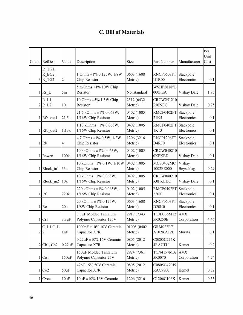
C. Bill of Materials
Count RefDes Value Description Size Part Number Manufacturer
Per Unit Cost
3
R_TG1, R_BG2, R_TG2 2
1 Ohms ±1% 0.125W, 1/8W Chip Resistor
0603 (1608 Metric)
RNCP0603FTD1R00
Stackpole Electronics 0.1
1 Rs_L 5m 5 mOhms ±1% 10W Chip Resistor Nonstandard
WSHP28185L000FEA Vishay Dale 1.95
2 R_L1, R_L2 10
10 Ohms ±5% 1.5W Chip Resistor
2512 (6432 Metric)
CRCW251210R0JNEG Vishay Dale 0.75
1 Rfb_out1 21.5k 21.5 kOhms ±1% 0.063W, 1/16W Chip Resistor
0402 (1005 Metric)
RMCF0402FT21K5
Stackpole Electronics 0.1
1 Rfb_out2 1.13k 1.13 kOhms ±1% 0.063W, 1/16W Chip Resistor
0402 (1005 Metric)
RMCF0402FT1K13
Stackpole Electronics 0.1
1 Rb 4 4.7 Ohms ±1% 0.5W, 1/2W Chip Resistor
1206 (3216 Metric)
RNCP1206FTD4R70
Stackpole Electronics 0.1
1 Rswen 100k 100 kOhms ±1% 0.063W, 1/16W Chip Resistor
0402 (1005 Metric)
CRCW0402100KFKED Vishay Dale 0.1
1 Rlock_in1 33k 10 kOhms ±1% 0.1W, 1/10W Chip Resistor
0402 (1005 Metric)
MCS0402MC1002FE000
Vishay Beyschlag 0.29
1 Rlock_in2 10k 10 kOhms ±1% 0.063W, 1/16W Chip Resistor
0402 (1005 Metric)
CRCW040210K0FKEDC Vishay Dale 0.1
1 Rf 220k 220 kOhms ±1% 0.063W, 1/16W Chip Resistor
0402 (1005 Metric)
RMCF0402FT220K
Stackpole Electronics 0.1
1 Rc 20k 20 kOhms ±1% 0.125W, 1/8W Chip Resistor
0603 (1608 Metric)
RNCP0603FTD20K0
Stackpole Electronics 0.1
1 Ci1 3.3uF 3.3µF Molded Tantalum Polymer Capacitor 125V
2917 (7343 Metric)
TCJD335M125R0250E
AVX Corporation 4.46
2 C_L1,C_L2 1nF
1000pF ±10% 10V Ceramic Capacitor X7R
01005 (0402 Metric)
GRM022R71A102KA12L Murata 0.1
2 Cb1, Cb2 0.22uF 0.22µF ±10% 16V Ceramic Capacitor X7R
0805 (2012 Metric)
C0805C224K4RACTU Kemet 0.2
1 Co1 150uF 150µF Molded Tantalum Polymer Capacitor 25V
2924 (7361 Metric)
TCN4157M025R0070
AVX Corporation 4.74
1 Co2 50uF 47pF ±5% 50V Ceramic Capacitor X7R
0805 (2012 Metric)
C0805C470J5RAC7800 Kemet 0.32
1 Cvcc 10uF 10µF ±10% 16V Ceramic 1206 (3216 C1206C106K Kemet 0.33

47
Capacitor X7R Metric) 4RACTU
1 C_LDO 1uF 1µF ±10% 6.3V Ceramic Capacitor X7R
0603 (1608 Metric)
C0603C105K9RACTU Kemet 0.29
1 Cc1 3.3nF 3300pF ±10% 10V Ceramic Capacitor X7R
0402 (1005 Metric)
C0402C332K8RAC7867 Kemet 0.42
1 Cc2 330pF 330pF ±10% 10V Ceramic Capacitor X7R
0402 (1005 Metric)
C0402C331K8RAC7867 Kemet 0.42
1 Css 100nF 0.1µF ±10% 16V Ceramic Capacitor X7R
0402 (1005 Metric)
GRM155R71C104KA88J
Murata Electronics 0.1
1 Cvi 1uF 1µF ±10% 250V Ceramic Capacitor X7R
2220 (5750 Metric)
GRM55DR72E105KW01L
Murata Electronics 1.73
1 DB1 Diode Standard 125V 200mA Surface Mount
2-SMD, No Lead BAQ335-TR Vishay 0.33
1 DB2 Diode Standard 125V 200mA Surface Mount
2-SMD, No Lead BAQ335-TR Vishay 0.33
1 L 15uH 15µH Shielded Wirewound Inductor 36A 1.441mOhm
Max Nonstandard 74436411500
Würth Elektronik 8.11
4
MT1, MB1, MB3, MT2
N-Channel 80V 90A (Tc) 150W (Tc) Surface Mount
TO-252-3, DPak (2 Leads + Tab), SC-63
IPD053N08N3GATMA1
Infineon Technologies 2.1
2 Dp1, Dp2 Diode Standard 30V 15A Surface Mount
DDPAK/TO-263-3
SM74611KTTR
Texas Instruments 3.5
Total: 42.32

48
D. Analysis of Senior Project Design
Project Title: MISO DC/DC Farmbot
Students: Astha Adhikari, Brian Armijo, Quyen Nguyen
Advisor: Dr. Taufik
1. Summary of Functional Requirements
The MISO Farmbot is a DC to DC power converter with a universal input that functions in
isolation. The contained component includes a multi-input stage, a power conversion stage, a control
stage, and an information relay stage. The device will function without any connection to the grid and will
handle quick switching between inputs via parallel diodes. The input range will contain the expected
voltage and current of renewable energy sources while the output is specified by the customer. The main
purpose of the MISO Farmbot is to allow use of renewable energy sources independent of the grid.
2. Primary Constraints
Most technical constraints fall under electrical specifications. The Farmbot must take an input of
10V -70V, and output 24V at a max power rating of 120W. Storing unused power in batteries allows long
term use of generated energy. To efficiently deliver dependable energy conversion, the device must
handle the full range of natural occurring weather conditions while maintaining a price tag at around
$150.
3. Economic
(a) Human Capital: The Farmbot will create engineering, technician, and customer service
jobs surrounding the small-scale energy conversion industry. Enabling private customers and

49
businesses to flourish will help smaller communities gain a foothold in financial and renewable
markets.
(b) Financial Capital: This product’s price tag allows an almost limitless market for any rural
customers looking to make the most of renewable energy sources. A small part of buck is passed
from those installing energy production to the seller of this Farmbot. The rest of the payoff goes
to the customer as this power converter cuts out a lot of unnecessary grid-tied infrastructure.
(c) Natural Capital: Electronic devices do not recycle well, but the surrounding mechanical
containment will scrap into standard reusability establishments. Minimizing material will come
naturally by maximizing efficiency of device cost and power conversion.
(d) Cost and Timing: The Farmbot DC/DC converter will cost $150 at a quantity of 100
modules sold. This price tag and sales magnitude will come within 5 years of device release. The
prototype is expected to be complete by May 2020. A commercially available version will come
after a year of testing.
4. If manufactured on a commercial basis:
(a) Estimated Number of devices first year: 100-300 units
(b) Estimated Number of devices at 2-5 years: 2000-10000 units
(c) Estimated Number of devices after 5 years: 100k-200k units
(d) Estimated manufacturing cost for each device: $45
(e) Estimated purchase price for each for each unit: $150
(f) Estimated profit 1st year, 2-5 years, and 5+ years: $15,000, $450,000, $11 million
(g) Estimated Cost for User to operate devices: Ideally $0, subject to repairs

50
5. Environmental
The main environmental impact will come from the highly integrated electronic components
ending up in landfills at the end of the device lifetime. Minimizing non-recyclable materials will help
lower the negative material impact on the environment.
Electronic components mix Silicon and metal which ultimately come from mining practices. The
silicon specifically comes from gravel, is isolated in an arc furnace with a reduction process, then finally
cooled and crushed with use of slag. While the environmental impact of all this is significant, each
Farmbot module uses a physically small amount of material.
The contained device will not directly affect animals. Renewable energy production can make a
very small negative impact on the environment, but the alternative to renewable sources is much more
costly to species life.
5. Manufacturability
Manufacturing will happen in a 2-stage process: electronic compilation and physical construction.
The Farmbot requires a period between electronic and physical production for testing. A device that meets
electronic standards will continue to mechanical containment and finally physical testing.
6. Sustainability
The Farmbot must handle the full range of environmental conditions. Without secure containment
around the device reliability cannot be guaranteed. A universal customer requires all temperatures,
precipitation, and minor physical perturbations. Long term protection from the environment is most
challenging at the connection between the device and the outside sources. Secure and watertight
connections are needed.

51
The Farmbot mainly cuts out the extensive wiring required for alternative power setups. The
device attains minimal material while offsetting bulking electronics.
At the current target market, the input range does not go above a voltage and current threshold
expected from private energy production. While more costly, an industry viable DC/DC converter would
handle one to two magnitudes higher of input. At the moment the target design is attempting to maximize
the relatively efficient customer market.
A magnitude of higher possible input will increase the cost while making relatively low power
input less efficient. Larger sub circuits, such as controller and RLC components, will mean a higher price
tag for production and the customer. To reasonably accommodate industry would mean lowering the
efficiency of private users. At the time it is very inefficient to try to meet both target customers with the
same device.
7. Ethical
The dangers of this product mainly come from the high-power levels incoming, in storage, and
outgoing from the device. Directly, the Farmbot has the potential to give off lethal amounts of current.
Indirectly, the electrical levels have the means to spark outside the device, which can start fires or harm
surrounding components. Financially, a power converter must remain safely functioning to keep all
surrounding electronic equipment from breaking.
8. Health and Safety
Private users rarely have the financial means to replace expensive electronic equipment, therefore
the Farmbot manufacturing process must take into account safety measures to avoid sending out incorrect
power. Many stages of a DC/DC converter contain safety levers to stop function if the circuit
malfunctions, including the controller containing both an input and output current sensing stage. Design
52
will also include tertiary safety measures to ensure disaster will not come if the device does not function
properly.
As students, this group project must contain a large amount of discipline in working towards
commercial standards. With help from advisors, the Farmbot design, simulation, and build will contain
many levels of checking to ensure no major flaws remain. We hope to work with each other and others to
ensure safety and reliability.
9. Social and Political
Thankfully, Cal Poly’s community, and California as a whole, welcome the use of renewable
energy positively. Enabling individual empowerment to make use of solar and turbine energy production
is at the forefront of the design team, the advisors, and many of the customers. The social agreement in
the use of something such as a Farmbot will only fail if safety or reliability becomes an issue.
The surrounding political environment mirrors the social atmosphere in wanting to make the most
of renewable energy sources. While many industry and private experts are unsure of the full scope of the
use of small-scale renewable, the Farmbot will fill in the gap that is left between grid-tied private
properties and rural environments.