semester: iv subject: computer systems architecture...
TRANSCRIPT

Semester: IV Branch: Computer Science & Engineering
Subject: Computer Systems Architecture Code: 322414 (22)
Total Theory Periods: 40 Total Tut Periods: 10
Total Marks in End Semester Exam: 80
Maximum number of Class Tests to be conducted: 2
Unit 1: Processor Basics
CPU Organization, Fundamental and features, Data Representation formats, Fixed and
Floating
point representation, Instruction Sets, Formats, Types and Programming Considerations.
Unit 2: Datapath Design
Fixed-Point Arithmetic, Combinational ALU and Sequential ALU, Floating point arithmetic
and
Advanced topics, Hardware Algorithm – Multiplication, Division.
Unit 3: Control Design Basic Concepts, Hardwired control, Microprogrammed Control, CPU control unit and Multiplier control unit, Pipeline Control.

Unit 4: Memory Organization
Memory device characteristics, RAM technology and Serial access memories
technology,
Multilevel memory systems, Address translation and Memory allocation systems,
Caches
memory.
Unit 5: System Organization
Programmed I/O , DMA, Interrupts and IO Processors, Processor-level Parallelism,
Multiprocessor and Fault tolerance system.
Name of Text Books
1. Computer Architecture and organization – John P Hayes, McGraw Hill Publication
2 Computer Organizations and Design- P. Pal Chaudhari, Prentice-Hall of India
Name of reference Books:
1. Computer System Architecture - M. Morris Mano, PHI.
2. Computer Organization and Architecture- William Stallings, Prentice-Hall of India
3. Architecture of Computer Hardware and System Software: An Information Technology
Approach,
3rd Edition (Illustrated) – Iry Englander, John Wiley & Sons Inc
4 Structured Computer Organization Andrew S Tanenbaum, Prentice-Hall of India
5 Computer Systems Organization & Architecture – John D Carpinelli, Addison-Wesle


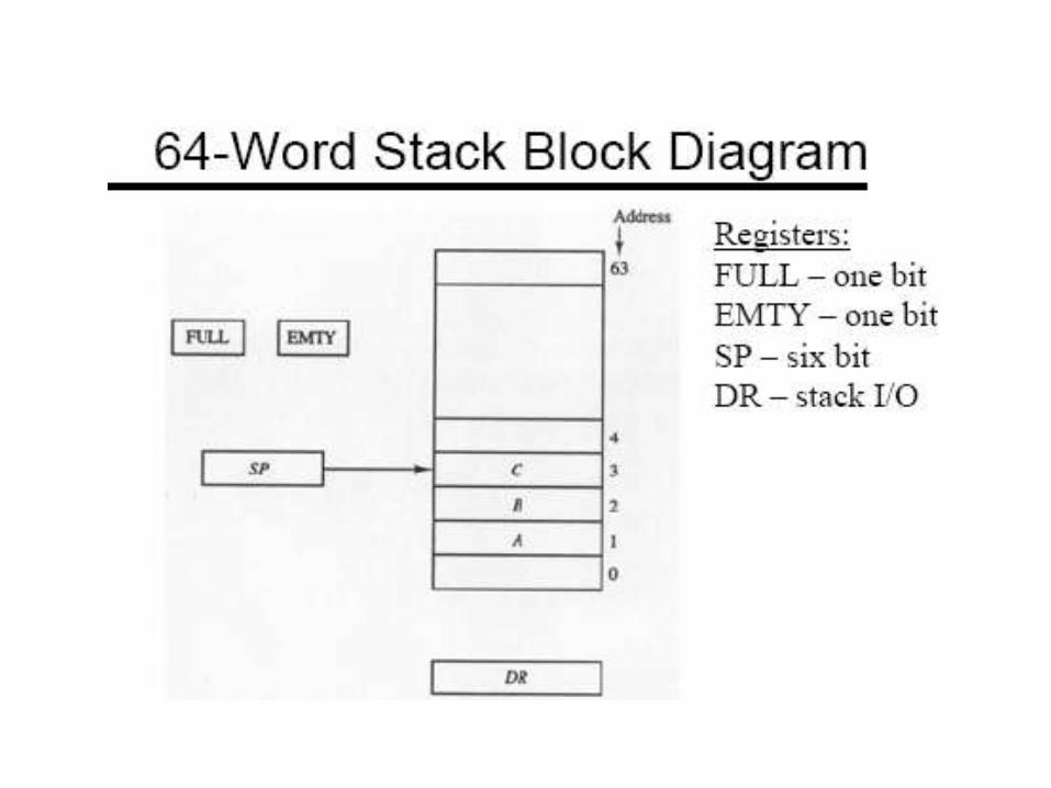
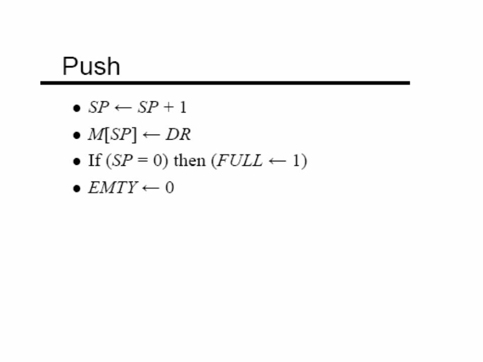
Unit - 02 Principles of Computer
design

Register Organization


Determining The Type of Instruction


Elements of an Instruction
• Operation code (Op code)
– Do this
• Source Operand reference
– To this
• Result Operand reference
– Put the answer here
• Next Instruction Reference
– When you have done that, do this...

Where have all the Operands gone?
• Main memory (or virtual memory or cache)
• CPU register
• I/O device

Instruction Representation
OPCODE OPERAND1 OPERAND2

Instruction Types
• Data processing
• Data storage (main memory)
• Data movement (I/O)
• Program flow control

Number of Addresses (a)
• 3 addresses
– Operand 1, Operand 2, Result
– a = b + c;
– May be a forth - next instruction (usually implicit)
– Not common
– Needs very long words to hold everything

Number of Addresses (b)
• 2 addresses
– One address doubles as operand and result
– a = a + b
– Reduces length of instruction
– Requires some extra work
• Temporary storage to hold some results

Number of Addresses (c)
• 1 address
– Implicit second address
– Usually a register (accumulator)
– Common on early machines

Number of Addresses (d)
• 0 (zero) addresses – All addresses implicit
– Uses a stack
– e.g. push a
– push b
– add
– pop c
– c = a + b

How Many Addresses
• More addresses – More complex (powerful?) instructions
– More registers • Inter-register operations are quicker
– Fewer instructions per program
• Fewer addresses – Less complex (powerful?) instructions
– More instructions per program
– Faster fetch/execution of instructions

Design Decisions (1)
• Operation repertoire
– How many ops?
– What can they do?
– How complex are they?
• Data types
• Instruction formats
– Length of op code field
– Number of addresses

Design Decisions (2)
• Registers
– Number of CPU registers available
– Which operations can be performed on which registers?
• Addressing modes (later…)
• RISC v CISC

136
Instruction cycle with interrupt

137
Interrupts - In Summary
• An interruption of normal processing
• Improves processing efficiency
• Allows the processor to execute other instructions while an I/O operation is in progress
• A suspension of a process caused by an event external to that process and performed in such a way that the process can be resumed

138
Classes of Interrupts • Program
– arithmetic overflow
– division by zero
– execute illegal instruction
– reference outside user’s memory space
• Timer
• I/O
• Hardware failure

139
Common Functions of Interrupts
• Interrupts transfer control to the interrupt service routine generally, through the interrupt vector
• Interrupt architecture must save the address of the interrupted instruction.
• interrupts are disabled while another interrupt is being processed to prevent a lost interrupt.
• A trap is a software-generated interrupt caused either by an error or a user request.
• An operating system is interrupt driven.

140
Interrupt Handling • The operating system preserves the state of the
CPU by storing registers and the program counter.
• Determines which type of interrupt has occurred:
– polling
– vectored interrupt system
• Separate segments of code determine what action should be taken for each type of interrupt

141
Instruction Cycle with Interrupts
Fetch Next
Instruction
Execute
Instruction START
HALT
Fetch Cycle Execute Cycle
Check for &
Process Int
Interrupt Cycle
Inte
rru
pts
En
ab
led
Interrupts Disabled

142
Interrupt Cycle
• Processor checks for interrupts
• If no interrupts fetch the next instruction for the current program
• If an interrupt is pending, suspend execution of the current program, and execute the interrupt handler

143
Interrupt Service Routine (aka handler)
• A program that determines nature of the interrupt and performs whatever actions are needed
• Control is transferred to this program
• Generally part of the operating system
144
Simple Interrupt Processing
Device controller or
other system hardware
issues an interrupt
Processor finishes
execution of current
instruction
Processor signals
acknowledgment
of interrupt
Processor pushes PSW
and PC onto control
stack
Processor loads new
PC value based on
interrupt
Save remainder of
process state
information
Process interrupt
Restore process state
information
Restore old PSW
and PC
Hardware Software

145
What about Multiple Interrupts
• Simple Approach - disable interrupts
• Use Priorities to differentiate between interrupt classes

146
Multiple Interrupts Sequential Order
• Disable interrupts so processor can complete task
• Interrupts remain pending until the processor enables interrupts
• After interrupt handler routine completes, the processor checks for additional interrupts

147
Multiple Interrupts Priorities
• Higher priority interrupts cause lower-priority interrupts to wait
• Causes a lower-priority interrupt handler to be interrupted
• Example when input arrives from communication line, it needs to be absorbed quickly to make room for more input

Unit – 03 CPU
&
Control Unit


Instruction Formats The format of an instruction is usually depicted in a
rectangular box symbolizing the bits of the instruction as they appear in memory words or in a control register. The bits of the instructions are divided into groups called fields. The most common fields found in instruction format are:-
1. An Operation code field that specifies the operation to be performed.
2. An address field that designates a memory address or a processor register.
3. A mode field that specifies the way the operand or the effective address is determined.
Computer may have instructions of several different length containing varying number of addresses. The no. of address field in the instruction format of a computer depends on the internal organization of its registers.


Addressing Modes


RISC vs CISC RISC
Emphasis on hardware Includes multi-clock
complex instructions Memory-to-memory:
"LOAD" and "STORE“
incorporated in instructions Small code sizes,
high cycles per second Transistors used for storing
complex instructions
CISC
Emphasis on software Single-clock,
reduced instruction only Register to register:
"LOAD" and "STORE“
are independent instructions Low cycles per second,
large code sizes Spends more transistors
on memory registers

CISC Characteristics
• The instructions in a typical CISC processor provide direct manipulation of operands residing in a memory. The major characteristics of CISC architecture are:-
1. A large number of instructions – typically from 100 to 250 instructions
2. Some instruction that perform specialized tasks and are used infrequently
3. A large variety of addressing modes – typically from 5 to 20 different modes
4. Variable – length instruction format 5. Instruction that manipulate operands in memory 6. Instructions are complex 7. Example - Pentium processors.

RISC Characteristics • The concept of RISC architecture involves an attempt to
reduce execution time by simplifying the instruction set of the computer. The major characteristics of a RISC processor are:
1. Relatively few instructions 2. Relatively few addressing modes 3. Memory access limited to load and store instructions 4. All operation done within the register of the CPU 5. Fixed length, easily decoded instruction format. 6. Single cycle instruction execution 7. Hardwired rather than Micro programmed control 8. Instructions are simple 9. Example:- Power PC.


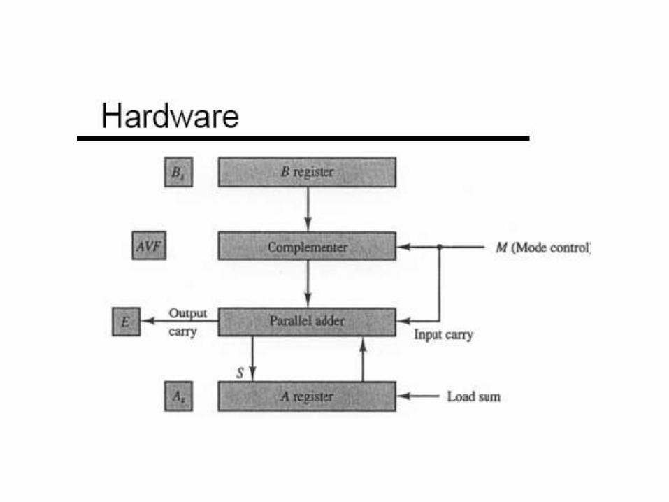
Address logic
Control
memory
Microinstruction register
Instruction
register
Decoder
Status signals
Control signals
General structure for Microprogrammed control unit

Sequential logic circuit
Instruction register
Status signals
Control signals
General structure for hardwired control unit

The hardwired approach views the controller as a sequential logic circuit or finite state machine that generates specific sequences of control signals
Advantage: 1. reduces the number of components
2. speed is fast
Disadvantage : Once the unit is constructed the only way to implement changes in control unit behaviour is by redesigning the entire unit
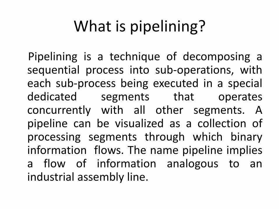
What is pipelining?
Pipelining is a technique of decomposing a sequential process into sub-operations, with each sub-process being executed in a special dedicated segments that operates concurrently with all other segments. A pipeline can be visualized as a collection of processing segments through which binary information flows. The name pipeline implies a flow of information analogous to an industrial assembly line.

Pipelining Example
• Sub-operation performed in each segment of the pipeline are as follows:-
R1 Ai, R2 Bi Input Ai and Bi
R3 R1 * R2, R4 Ci Multiply and input Ci
R5 R3 + R4 Add Ci to product

Pipelining Processing Ai Bi Ci
R1 R2
Multiplier
R3 R4
Adder
R5

Different Types of Pipelining • 1 Arithmetic pipeline
• 2 Instruction pipeline
• 3 RISC pipeline
• 4 Vector processing

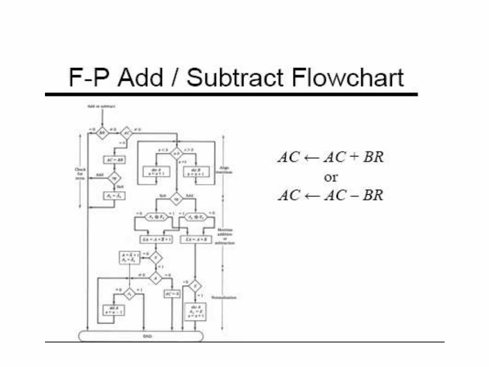
Arithmetic Pipeline
• An arithmetic pipeline divides an arithmetic operation into sub-operation for execution in the pipeline segments.
Pipeline arithmetic units are usually found in very high speed computers. They are used to implement floating-point operations, multiplication of fixed point numbers, and similar computations encountered in specific problems.

Pipeline for floating point Addition and Subtraction
R R
Compare exponents by subtraction
R
Choose exponents
Align mantissa
R
Exponent Mantissa
a1
a2
Segment 1
Segment 2

a1 a2
R
Adjust exponent
R
Add or subtract mantissa
R
Normalize result
R
Segment 4
Segment 3

Unit - 04
Computer Arithmetic
&
I/O Techniques


Combinational ALU

Combinational ALU

Combinational ALU

Combinational ALU

Sequential ALU

Sequential ALU Basic Design
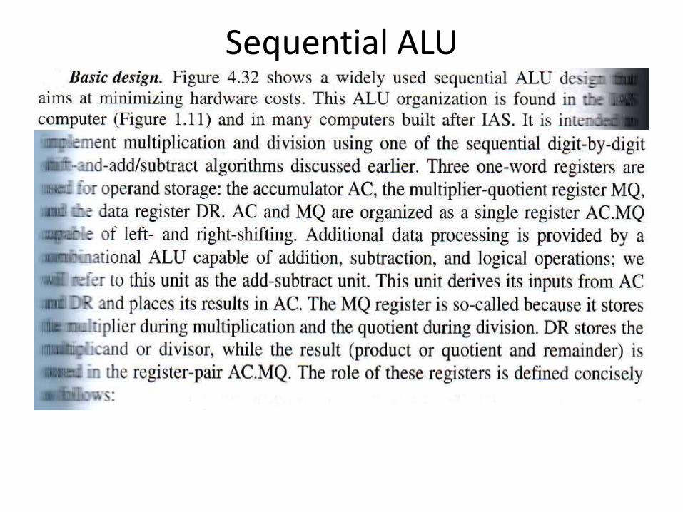
Sequential ALU

Sequential ALU

Register File

Register File

Floating Point Arithmatic

Basic Operation

Basic Operation

Basic Operation

Basic Operation

Algorithm for floating point Operation

Pipelined floating point operation


I/O Interface
Input-Output interface provides a method for transferring information between internal storage and external I/O devices. The purpose of the communication link is to resolve the differences that exist between the central computer and each peripheral. The major differences are :
1. Peripherals are electromechanical and electromagnetic devices and their manner of operation of the CPU and memory, which are electronic devices. Therefore, a conversion of signal values may be required.

2. The data transfer rate of peripherals is usually slower than the transfer rate of the CPU, and consequently, a synchronization mechanism may be needed.
3. Data codes and formats in peripherals differ from the word format in the CPU and memory.
4. The operating modes of peripheral are different from each other and each must be controlled so as not to disturb the operation of other peripherals connected to the CPU.

To resolve these differences computer systems include special hardware components between the CPU and peripherals to supervise and synchronize all input and output transfers. These components are called “interface units” because they interface between the processor bus and peripheral device. In addition each device may have its own controller that supervises the operation of the particular mechanism in the peripherals.
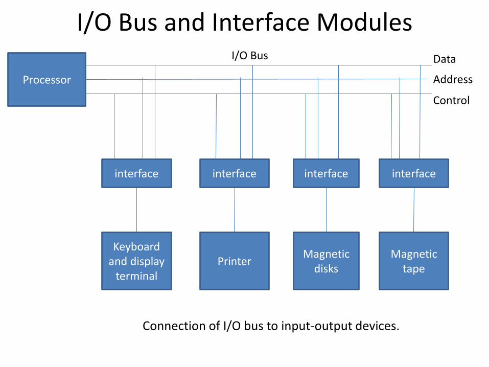
I/O Bus and Interface Modules
Connection of I/O bus to input-output devices.
Processor
interface interface interface interface
Keyboard and display
terminal Printer
Magnetic disks
Magnetic tape
Data
Address
Control
I/O Bus
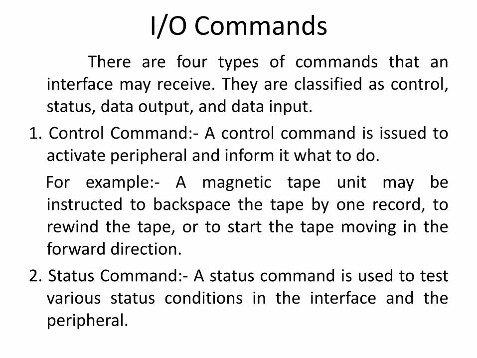
I/O Commands There are four types of commands that an
interface may receive. They are classified as control, status, data output, and data input.
1. Control Command:- A control command is issued to activate peripheral and inform it what to do.
For example:- A magnetic tape unit may be instructed to backspace the tape by one record, to rewind the tape, or to start the tape moving in the forward direction.
2. Status Command:- A status command is used to test various status conditions in the interface and the peripheral.

For example:- the computer may wish to check the status of the peripheral before a transfer is initiated. During the transfer, one or more errors may occur which are detected by the interface. These errors are designated by setting bits in a status register that the processor can read at certain intervals.
3. Output data:- It causes the interface to respond by transferring data from the bus into one of its register. Consider an example with a tape unit. The computer starts the tape moving by issuing a control command.

The processor then monitor the status of the tape by means of a status command. When the tape is in the correct position the processor issues a data output command. The interface responds to the address and command and transfers the information from the data lines in the bus to its buffer register. The interface then communicates with the tape controller and sends the data to be stored on tape.

4. Input data:- The data input command is the opposite of the data output. In this case the interface receive an item of data from the peripheral and places it in its buffer register. The processor checks if data are available by means of a status command and then issues a data input command. The interface places the data on the data lines, where they are accepted by the processor.

Example of I/O Interface
Port A
register
Port B register
Control register
Status register
Bus buffers
CS RS1 Timing
and RS0 control
RD
WR
To CPU To I/P devices
I/O data
I/O data
Control
Status
Bidirectional
Data bus
Chip select
Regular select
I/O read
I/O write
In
te
rn
al
b
us

Example of I/O Interface unit
CS RS1 RS0
Register selected
0 * * 1 0 0 1 0 1 1 1 0 1 1 1
None: data bus in high impedance Port A register Port B register Control register Status register

Synchronization
• The process that communicate, do so through a synchronization mechanism. A process executes with unpredictable velocity and generates events and actions that must be recognized by other co-operating processes. The set of constraints on the ordering of these events constitutes the set of synchronization required for the operating processes. The synchronization technique is used to delay execution of a process in order to satisfy such constraints.
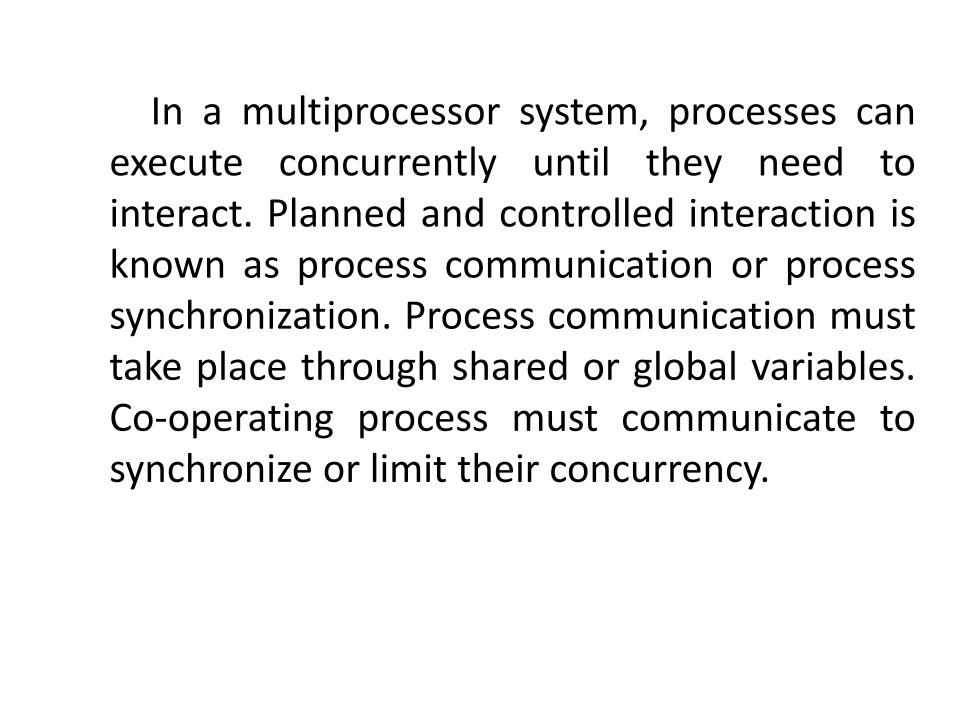
In a multiprocessor system, processes can execute concurrently until they need to interact. Planned and controlled interaction is known as process communication or process synchronization. Process communication must take place through shared or global variables. Co-operating process must communicate to synchronize or limit their concurrency.

Two types of synchronization are generally needed while using shared variable.
1. Mutual Exclusion :- Mutual exclusion ensures that a physical or virtual resource is held indivisibly.
2. Condition Synchronization :- When a shared data object is in a state that is not appropriate for executing a given operation, any process which attempts such an operation must be delayed. Such operation must be delayed until the state of data objects to the desired value as a result of other process being executed. This type of synchronization is called “ Condition synchronization”.

Input Output Techniques
• Programmed
• Interrupt driven
• Direct Memory Access (DMA)

Three Techniques for Input of a Block of Data

Programmed I/O
• CPU has direct control over I/O
– Sensing status
– Read/write commands
– Transferring data
• CPU waits for I/O module to complete operation
• Wastes CPU time

Programmed I/O - detail
• CPU requests I/O operation
• I/O module performs operation
• I/O module sets status bits
• CPU checks status bits periodically
• I/O module does not inform CPU directly
• I/O module does not interrupt CPU
• CPU may wait or come back later

Programmed I/O Programmed I/O operations are the result of
I/O instructions written in the computer program. Each data item transfer is initiated by an instruction in the program. Usually the transfer is to read and from a CPU register and peripheral. Other instructions are needed to transfer the data to and from CPU and memory. Transferring data under program control requires constant monitoring of the peripheral by the CPU. Once a data transfer is initiated, the CPU is required to monitor the interface to see when a transfer can again be made.

Example of Programmed I/O
In the programmed I/O method, the I/O devices does not have direct access to memory. A transfer from an I/O device to memory requires the execution of several instruction by the CPU, including an input instruction to transfer the data from the device to the CPU and a store instruction to transfer the data from the CPU to memory. Other instruction may be needed to verify that the data are available from the device and to count the numbers of words transferred.

An example of data transfer from an I/O device through an interface into the CPU is shown in figure:-
CPU
Interface
Data register
Status F register
I/O device
I/O bus
Data valid
Data accepted
Data bus
Address bus
I/O read
I/O write
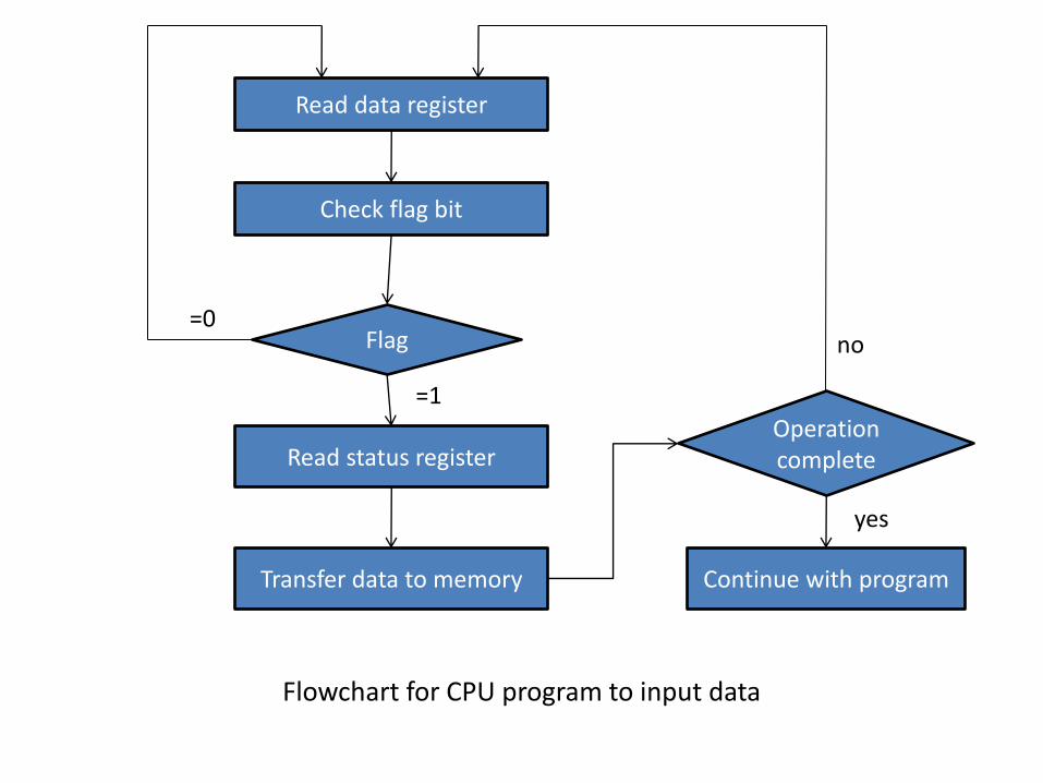
Flowchart for CPU program to input data
Read data register
Check flag bit
Flag
Read status register
Transfer data to memory
Operation complete
Continue with program
=0
=1
no
yes

I/O Commands
• CPU issues address – Identifies module (& device if >1 per module)
• CPU issues command – Control - telling module what to do
• e.g. spin up disk
– Test - check status • e.g. power? Error?
– Read/Write • Module transfers data via buffer from/to device

Addressing I/O Devices
• Under programmed I/O data transfer is very like memory access (CPU viewpoint)
• Each device given unique identifier
• CPU commands contain identifier (address)

I/O Mapping
• Memory mapped I/O – Devices and memory share an address space
– I/O looks just like memory read/write
– No special commands for I/O
• Large selection of memory access commands available
• Isolated I/O – Separate address spaces
– Need I/O or memory select lines
– Special commands for I/O
• Limited set

Memory Mapped and Isolated I/O

Interrupt Mechanism
Data transfer between the CPU and I/O device is initiated by the CPU. However, the CPU can not start the transfer unless the device is ready to communicate with the CPU. The readiness of the device can be determined from an interrupt signal. The CPU respond to the Interrupt request by storing the return address from PC into a memory stack and then the program branches to service routine that processes the required transfer.

Priority Interrupt A priority interrupt is a system that establishes a
priority over the various sources to determine which condition is to be services first when two or more request arrive simultaneously. The system may also determine which condition are permitted to interrupt the computer while another interrupt is being serviced. Higher – priority interrupt levels are assigned to request which, if delayed or interrupted, could have serious consequences. Device with high speed transfer such as magnetic disk are given high priority. When two devices interrupt the computer at the same time, the computer services the device, with the higher priority first.

Polling Establishing the priority of simultaneous
interrupts can be done by software or hardware. A polling procedure is used to identify the highest priority source by software means. In this method there is a one common branch address for all interrupts. The program that take care of interrupt begin at the branch address and polls the interrupt source in sequence. The order in which they are tested determines the priority of each interrupt. The highest priority interrupt is tested first, and if its interrupt signal is on, control branches to service routine for this source. Otherwise the next lower priority source is tested, and so on.

Daisy-Chaining Priority The hardware priority interrupt can be
established by either a serial or parallel connection of interrupt lines. The serial connection is also known as the daisy chaining method.
The daisy chaining method of establishing priority consist of a serial connection of all devices that request an interrupt. The device with the highest priority is places in the first position followed by lower priority devices up to the device with the lowest priority, which is places last in the chain. The method of connection between three devices and the CPU is shown in figure:-

Daisy-Chaining Priority Interrupt
Device 1 PI PO
Device 2 PI PO
Device 3 PI PO
Interrupt request
Interrupt acknowledge
CPU
INTACK
INT
VAD 1 VAD 2 VAD 3
To next device
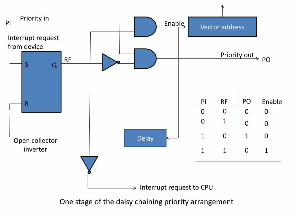
One stage of the daisy chaining priority arrangement
Vector address
Delay
Enable PI Priority in
Priority out PO
Interrupt request to CPU
RF
Open collector inverter
Interrupt request from device
S
R
Q
PI PO RF Enable
0
1
0 0 0
0
0
0
0 0
0 1
1
1
1 1

Priority Interrupt Hardware
0
1
2
3
0
0
0
0
0
0
0
1
2
3
IST IEN
Interrupt to CPU
INTACK from CPU
Enable
Mask Register
Priority encoder
VAD to CPU
Interrupt register
Disk
Printer
Reader
Keyboard
I0
I1
I2
I3
y
x

Interrupt Driven I/O
• Overcomes CPU waiting
• No repeated CPU checking of device
• I/O module interrupts when ready

Interrupt Driven I/O Basic Operation
• CPU issues read command
• I/O module gets data from peripheral whilst CPU does other work
• I/O module interrupts CPU
• CPU requests data
• I/O module transfers data

Simple Interrupt Processing

Direct Memory Access (DMA)
The transfer of data between a fast storage device such as magnetic disk and memory is often limited by the speed of the CPU. Removing the CPU from the path and letting the peripheral device manage the memory buses directly would improve the speed of transfer. This transfer technique is called direct memory access (DMA). During DMA transfer the CPU is idle and has no control of the memory buses. A DMA controller takes over the buses to manage the transfer directly between the I/O devices and memory.

CPU bus signals for DMA transfer
Address bus
Data bus
Read
Write
Bus request
Bus grant
BR
BG
DBUS
ABUS
RD
WR
High Impedance (disable) When BG is enabled

Block diagram of DMA controller
Data bus buffer
Address bus buffer
Address register
Word count register
Control register
DMA request
DMA Acknowledge To I/O device
Interrupt
Bus grant
Bus request
Write
Read
Register select
DMA select
Data bus
Address bus
Internal bus

DMA transfer in a computer system
CPU RAM
DMA controller
I/O Peripheral
device
Address select
RD
WR
DS
RS
BR BG
Address Data WR
RD RD WR Address Address Data Data
Interrupt
BG
BR
Interrupt
Address bus
Data bus
Write control
Read control
DMA acknowledge
DMA request

Direct Memory Access
• Interrupt driven and programmed I/O require active CPU intervention
– Transfer rate is limited
– CPU is tied up
• DMA is the answer

DMA Function
• Additional Module (hardware) on bus
• DMA controller takes over from CPU for I/O

Typical DMA Module Diagram

DMA Operation
• CPU tells DMA controller:-
– Read/Write
– Device address
– Starting address of memory block for data
– Amount of data to be transferred
• CPU carries on with other work
• DMA controller deals with transfer
• DMA controller sends interrupt when finished

DMA Transfer Cycle Stealing
• DMA controller takes over bus for a cycle
• Transfer of one word of data
• Not an interrupt – CPU does not switch context
• CPU suspended just before it accesses bus – i.e. before an operand or data fetch or a data
write
• Slows down CPU but not as much as CPU doing transfer

DMA and Interrupt Breakpoints During an Instruction Cycle

DMA Configurations (1)
• Single Bus, Detached DMA controller
• Each transfer uses bus twice – I/O to DMA then DMA to memory
• CPU is suspended twice
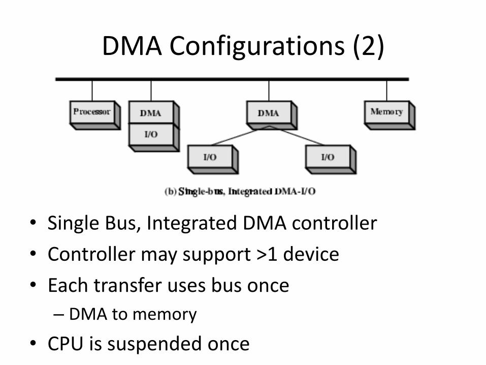
DMA Configurations (2)
• Single Bus, Integrated DMA controller
• Controller may support >1 device
• Each transfer uses bus once
– DMA to memory
• CPU is suspended once

DMA Configurations (3)
• Separate I/O Bus
• Bus supports all DMA enabled devices
• Each transfer uses bus once – DMA to memory
• CPU is suspended once

Intel 8237A DMA Controller
• Interfaces to 80x86 family and DRAM
• When DMA module needs buses it sends HOLD signal to processor
• CPU responds HLDA (hold acknowledge) – DMA module can use buses
• E.g. transfer data from memory to disk 1. Device requests service of DMA by pulling DREQ (DMA request) high
2. DMA puts high on HRQ (hold request),
3. CPU finishes present bus cycle (not necessarily present instruction) and puts high on HDLA (hold acknowledge). HOLD remains active for duration of DMA
4. DMA activates DACK (DMA acknowledge), telling device to start transfer
5. DMA starts transfer by putting address of first byte on address bus and activating MEMR; it then activates IOW to write to peripheral. DMA decrements counter and increments address pointer. Repeat until count reaches zero
6. DMA deactivates HRQ, giving bus back to CPU

8237 DMA Usage of Systems Bus


Instruction pipeline
An Instruction pipeline operates on a stream of instructions by overlapping the fetch, decode, and execute phases of instruction cycle.
The instruction pipeline reads consecutive instructions from memory while previous instruction are being executed in other segments. This type of unit that forms a queue rather than stack. The instructions are inserted into FIFO buffer so that they can be executed on a first in first out basis. Thus the instruction stream can be placed in a queue, waiting for decoding and processing by execution segment.

In most general case, the computer needs to process each instruction with the following sequence of steps:
1. Fetch the instruction from memory.
2. Decode the instruction.
3. Calculate the effective address.
4. Fetch the operands from memory.
5. Execute the instruction.
6. Store the result in the proper place.

Example –Four segment CPU pipeline
Segment 1
Segment 2
Fetch Instruction from memory
Decode instructions and
calculate effective address
Branch?
Fetch operand from memory
Interrupt?
Interrupt handling
Update PC
Empty pipe
Execute instruction
no
yes
no
yes
Segment 3
Segment 4

Pipeline Conflicts
There are three major difficulties that cause the instruction pipeline to deviate from its normal operation
1. Resource conflicts caused by access to memory by two segments at the same time. Most of these conflicts can be resolved by using separate instruction and data memories.
2. Data dependency conflicts arise when an instruction depends on the result of a previous instruction, but this result is not yet available.
3. Branch difficulties arise from branch and other instructions that change the value of PC.

Vector Processing
Vector processing used in vast number of computations that will take a conventional computer days or even weeks to complete. In many science and engineering applications, the problems can be formulated in terms of vector and matrices that land themselves to vector processing.

Use of vector processing
1 Long range weather forecasting. 2 Petroleum exploration. 3 Seismic data analysis. 4 Medical diagnosis. 5 Aerodynamics and space flight simulation. 6 Artificial Intelligence and expert systems. 7 Mapping the human genome. 8 Image processing.

What is Superscalar?
• Common instructions (arithmetic, load/store, conditional branch) can be initiated and executed independently
• Equally applicable to RISC & CISC
• In practice usually RISC

Why Superscalar?
• Most operations are on scalar quantities
• Improve these operations to get an overall improvement

Superpipelined
• Many pipeline stages need less than half a clock cycle
• Double internal clock speed gets two tasks per external clock cycle
• Superscalar allows parallel fetch execute


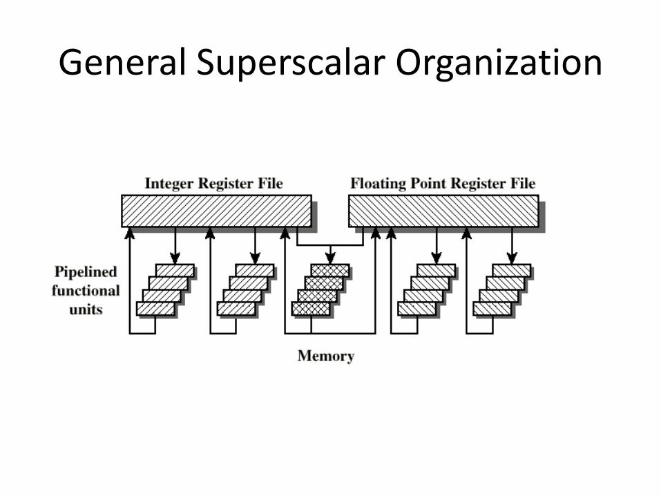
General Superscalar Organization

Superscalar v Superpipeline

Limitations
• Instruction level parallelism
• Compiler based optimisation
• Hardware techniques
• Limited by
– True data dependency
– Procedural dependency
– Resource conflicts
– Output dependency
– Antidependency

Unit – 05 Memory Systems
&
Multiprocessor

Semiconductor Memory
• RAM
– Misnamed as all semiconductor memory is random access
– Read/Write
– Volatile (contents are lost when power switched off)
– Temporary storage
– Static or dynamic
• Dynamic is based on capacitors – leaks thus needs refresh
• Static is based on flip-flops – no leaks, does not need refresh

Semiconductor Memory Types
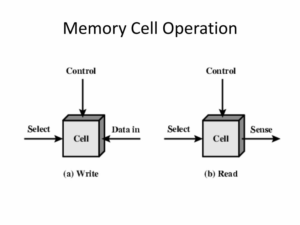
Memory Cell Operation


Dynamic RAM
• Bits stored as charge in capacitors • Charges leak • Need refreshing even when powered • Simpler construction • Smaller per bit • Less expensive • Need refresh circuits • Slower • Used in main memory • Essentially analogue
– Level of charge determines value

Dynamic RAM Structure

DRAM Operation
• Address line active when bit read or written – Transistor switch closed (current flows)
• Write – Voltage to bit line
• High for 1 low for 0
– Then signal address line • Transfers charge to capacitor
• Read – Address line selected
• transistor turns on
– Charge from capacitor fed via bit line to sense amplifier • Compares with reference value to determine 0 or 1
– Capacitor charge must be restored


Static RAM
• Bits stored as on/off switches • No charges to leak • No refreshing needed when powered • More complex construction • Larger per bit • More expensive • Does not need refresh circuits • Faster • Cache • Digital
– Uses flip-flops

Static RAM Structure

Static RAM Operation
• Transistor arrangement gives stable logic state • State 1
– C1 high, C2 low – T1 T4 off, T2 T3 on
• State 0 – C2 high, C1 low – T2 T3 off, T1 T4 on
• Address line transistors T5 T6 is switch • Write – apply value to B & compliment to B • Read – value is on line B

SRAM v DRAM
• Both volatile – Power needed to preserve data
• Dynamic cell – Simpler to build, smaller – More dense – Less expensive – Needs refresh – Larger memory units
• Static – Faster – Doesn’t need refresh – Cache – Consumes more power

372
Memory Hierarchy
• Major design objective - to provide adequate storage capacity
– at an acceptable level of performance
– at a reasonable cost
• The use of a hierarchy of storage devices can meet this goal:
• Registers internal to the CPU for temporary data storage (small in number but very fast) – External storage for data and programs (relatively large and fast)
– External permanent storage (much larger and much slower)
Memory

373
Typical memory hierarchy: (Technology, size, access time)
Registers
in CPU
Cache
(RAM, 100sKB, ~10ns)
Main memory
(RAM, 100sMB~GB, ~50ns)
Magnetic disk
(Hard disk, 10sGB-100sGB, ~10ms)
Optical disk
(CD-ROM, GB, ~100ms)
Magnetic tape
(Tape, 100sMB, sec-min)

374
• Each decreasing level in the hierarchy consists of modules of larger capacity, slower access time, and lower cost/bit.
• Goal of the memory hierarchy - try to match the processor speed with the rate of information transfer from the highest element in the hierarchy.
• The memory hierarchy works because of locality of reference
– Memory references made by the processor, for both instructions and data, tend to cluster together
» Instruction loops, subroutines
» Data arrays, tables
– Keep these clusters in high speed memory (e.g. cache memory) to reduce the average delay in accessing data;
– Over time, the clusters being referenced will change - memory management must deal with this (i.e. cache replacement).

375
Main Memory
• A main memory is a collection of words, used for storing programs or data; each word may consist of one or more bytes; conventionally, one word = two bytes.
• Physically, a memory of N words can be constructed using an N-word SRAM or DRAM, as described in the previous chapter.
• Logically, a memory of N words is like an array of N elements in Java or any other high-level language; e.g. a 10-element array in Java: int MEM = new int[10].
• A byte or word in a memory is often called a memory cell. Each cell in the memory can be located individually by its address, and thus written to or read from.
• The difference between an address and what is stored at that address cannot be over-emphasized; e.g. address $1000 may contain any bit pattern.
376
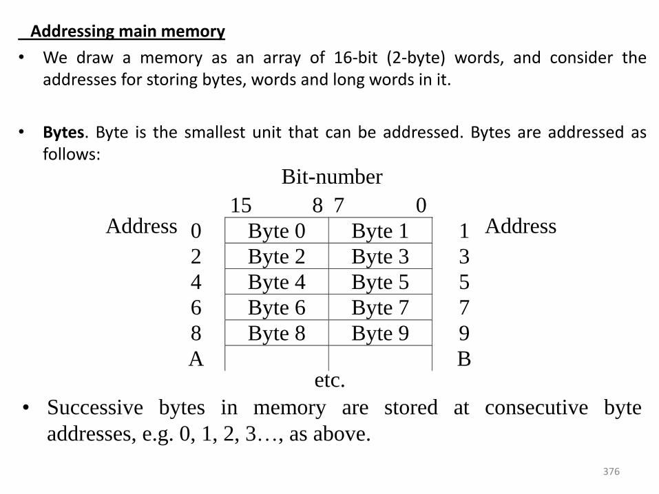
Addressing main memory
• We draw a memory as an array of 16-bit (2-byte) words, and consider the addresses for storing bytes, words and long words in it.
• Bytes. Byte is the smallest unit that can be addressed. Bytes are addressed as follows:
• Successive bytes in memory are stored at consecutive byte
addresses, e.g. 0, 1, 2, 3…, as above.
15 8 7 0
0 Byte 0 Byte 1 1
2 Byte 2 Byte 3 3
4 Byte 4 Byte 5 5
6 Byte 6 Byte 7 7
8 Byte 8 Byte 9 9
A B
Bit-number
Address
etc.
Address

377
• Words. Each consists of 2 bytes, addressed as follows:
• Words are stored and accessed at even addresses (at even byte
numbers), e.g. 0, 2, 4, 6…, as above.
Byte 0 Byte 1
MSB Bit-number
Address
etc.
First
byte Second
byte
15 0
0 Word 0 1
2 Word 2 3
4 Word 4 5
6 Word 6 7
8 Word 8 9
A B

378
• Long words. Each consists of 4 bytes, addressed as follows:
• Long words are stored and accessed at even addresses that are
multiple of 4, e.g. 0, 4, 8, C…, as above.
Byte 0 Byte 1 Byte 2 Byte 3
MSB Bit-number
Address
etc.
First
byte Last
byte
15 0
0 1
2
Long
word 0 3
4 5
6
Long
word 4 7
8 9
A
Long
word 8 B


Cache
• Small amount of fast memory
• Sits between normal main memory and CPU
• May be located on CPU chip or module

Cache/Main Memory Structure


Associative Mapping
• A main memory block can load into any line of cache
• Memory address is interpreted as tag and word
• Tag uniquely identifies block of memory
• Every line’s tag is examined for a match
• Cache searching gets expensive

Fully Associative Cache Organization

Associative Mapping Example

Tag 22 bit Word 2 bit
Associative Mapping Address Structure
• 22 bit tag stored with each 32 bit block of data
• Compare tag field with tag entry in cache to check for hit
• Least significant 2 bits of address identify which 16 bit word is required from 32 bit data block
• e.g. – Address Tag Data Cache line
– FFFFFC FFFFFC 24682468 3FFF

Associative Mapping Summary
• Address length = (s + w) bits
• Number of addressable units = 2s+w words or bytes
• Block size = line size = 2w words or bytes
• Number of blocks in main memory = 2s+ w/2w = 2s
• Number of lines in cache = undetermined
• Size of tag = s bits


Direct Mapping
• Each block of main memory maps to only one cache line
– i.e. if a block is in cache, it must be in one specific place
• Address is in two parts
• Least Significant w bits identify unique word
• Most Significant s bits specify one memory block
• The MSBs are split into a cache line field r and a tag of s-r (most significant)
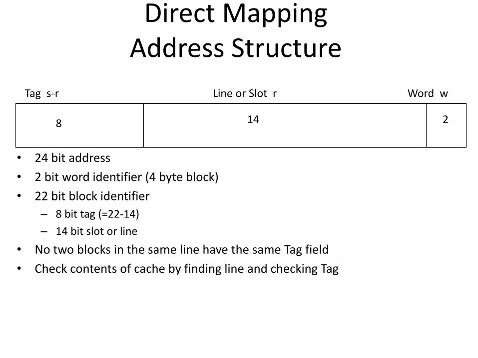
Direct Mapping Address Structure
Tag s-r Line or Slot r Word w
8 14 2
• 24 bit address
• 2 bit word identifier (4 byte block)
• 22 bit block identifier
– 8 bit tag (=22-14)
– 14 bit slot or line
• No two blocks in the same line have the same Tag field
• Check contents of cache by finding line and checking Tag

Direct Mapping Cache Line Table
• Cache line Main Memory blocks held
• 0 0, m, 2m, 3m…2s-m
• 1 1,m+1, 2m+1…2s-m+1
• m-1 m-1, 2m-1,3m-1…2s-1

Direct Mapping Cache Organization

Direct Mapping Example

Direct Mapping Summary
• Address length = (s + w) bits
• Number of addressable units = 2s+w words or bytes
• Block size = line size = 2w words or bytes
• Number of blocks in main memory = 2s+ w/2w = 2s
• Number of lines in cache = m = 2r
• Size of tag = (s – r) bits

Direct Mapping pros & cons
• Simple
• Inexpensive
• Fixed location for given block
– If a program accesses 2 blocks that map to the same line repeatedly, cache misses are very high


Set Associative Mapping
• Cache is divided into a number of sets
• Each set contains a number of lines
• A given block maps to any line in a given set
– e.g. Block B can be in any line of set i
• e.g. 2 lines per set
– 2 way associative mapping
– A given block can be in one of 2 lines in only one set

Set Associative Mapping Example
• 13 bit set number
• Block number in main memory is modulo 213
• 000000, 00A000, 00B000, 00C000 … map to same set

Two Way Set Associative Cache Organization

Set Associative Mapping Address Structure
• Use set field to determine cache set to look in
• Compare tag field to see if we have a hit
• e.g
– Address Tag Data Set number
– 1FF 7FFC 1FF 12345678 1FFF
– 001 7FFC 001 11223344 1FFF
Tag 9 bit Set 13 bit Word 2 bit

Two Way Set
Associative Mapping Example
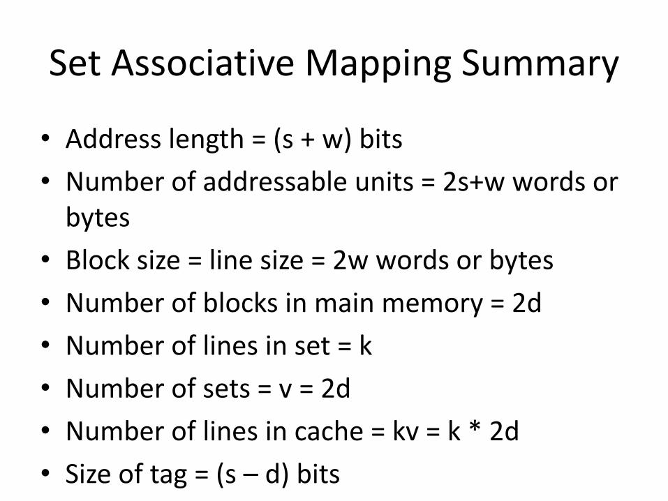
Set Associative Mapping Summary
• Address length = (s + w) bits
• Number of addressable units = 2s+w words or bytes
• Block size = line size = 2w words or bytes
• Number of blocks in main memory = 2d
• Number of lines in set = k
• Number of sets = v = 2d
• Number of lines in cache = kv = k * 2d
• Size of tag = (s – d) bits


Multiprocessors


Interprocessor Arbitration
Computer system contains a number of buses at various levels to
facilitate the transfer of information between components. The CPU
Contains a number of Internal buses for transferring information
between processor register and ALU. A memory bus consists of
lines for transferring data, address, and read/write information. An
I/O bus is used to transfer information to and from I/O devices.
System Bus:-
A bus that connects major components in a multi-processor system
such as CPUs, IOPs, memory, is called s system bus.

A typical system bus consists of approximately 100 signal lines.
These lines are divided into three functional groups: data, address,
and control.
In addition, there are power distribution lines that supply power to
the components.
For example, the IEEE standard 796 multibus system has 16 data
lines, 24 address lines, 26 control lines, and 20 power lines, for total
of 86 lines.
Data lines provide a path for the transfer of data between
processors and common memory.
Address lines are used to identify a memory address or any other
source or destination , such as input or output ports.
System Bus

Synchronous Bus & Asynchronous Bus
• Synchronous Bus
In a synchronous bus each data item is transferred during a time
slice known in advance to both source and destination units.
Synchronization is achieved by driving both units from a common
clock source.
• Asynchronous Bus
In an Asynchronous bus each data item being transferred is
accompanied by handshaking control signal to indicate when the
data are transferred from the source and achieved by the
destination.

• Control lines provide signals for controlling the information transfer between units . The signals indicate the validity of data and address
Information. Command signals specify operation to be performed. Typical control lines include transfer signals such as memory read and write , acknowledge of a transfer , Interrupt requests, bus control signal such as bus request and bus grant , and signals for arbitration procedures.

Serial Arbitration Procedure
Highest Lowest
Priority Priority
Bus PI PO
Arbiter 1
Bus
PI PO Arbiter 2
Bus PI PO
Arbiter 3
Bus PI PO
Arbiter 4
I
Bus busy line
To next arbiter
Serial (Daisy Chain ) arbitration

Parallel Arbitration Parallel arbitration
Bus arbiter 1
Ack Req
Bus arbiter 2
Ack Req
Bus arbiter 3
Ack Req
Bus arbiter 4
Ack Req
4*2 Priority encoder
2*4 Decoder
Bus busy line

Interprocessor Communication
• The various processors in a multiprocessor system must
be provided with a facility for communicating with each
other. A communication path can be established through
common input output channels. In a shared memory
multiprocessor system, the most common procedure is
to set aside a portion of a memory that is accessible to
all processors.
In addition to shared memory, a multiprocessor system
may have other shared resources. For example, a
magnetic disk storage unit connected to an IOP may be
available to all CPUs. This provides a facility for sharing
of system programs stored in the disk.

• There are three organizations that have been used in the design of operating system for multiprocessors:
• Master-slave configuration
• Separate operating system
• Distribute operating system

Master slave mode
• In a master slave mode, one processor, designated the master, always executes the operating system functions. If a slave processor needs an operating system service, it must request it by interrupting the master and waiting until the current program can be interrupted.

Separate operating system organization
• In the separate operating system organization, each processor can execute the operating system routines it needs. This organization is more suitable for loosely coupled systems where every processor may have its own copy of the entire operating system.

Distributed operating system organization
• In the distributed operating system organization, the operating system routines are distributed among the available processors. However particular operating system function is assigned to only one processor at a time. This type of operating system is also referred to as a floating operating system since the routines float from one processor to another and the execution of the routines may be assigned to defferent processors at different times.

Interprocessor synchronization
• The instruction set of a multiprocessor contains basic instruction that are used to implement communication and synchronization between cooperating processes. Communication refers to the exchange of data between different processes.
• Synchronization refers to the special case where the data used to communicate between processors is control information. Synchronization is needed to enforce the correct sequence of processes and to ensure mutually exclusive access to shared writable data.


Unit - 02 Principles of Computer
design