sed1520 cmos dot matrix lcd driver data sheet and design … · 7 s-mos systems, inc. 1.0 – 1.2.1...
TRANSCRIPT

1
S-MOS SYSTEMS, INC.
SED1520CMOS Dot Matrix LCD DriverData Sheet and Design Guide

2
S-MOS SYSTEMS, INC.
THIS PAGE INTENTIONALLY BLANK

3
S-MOS SYSTEMS, INC.
Table of Contents SED1520
Contents
1.0 Overview .................................................................................................................................................. 71.1 Description .................................................................................................................................... 71.2 Features ........................................................................................................................................ 7
1.2.1 SED1520 family specifications ....................................................................................... 71.3 Block Diagram ............................................................................................................................... 81.4 Package ........................................................................................................................................ 9
1.4.1 Pin Configuration Table .................................................................................................. 9
2.0 Pin Description ...................................................................................................................................... 132.1 Power Signals ............................................................................................................................. 132.2 System Bus Interface Signals ..................................................................................................... 132.3 LCD Drive Circuit Signals ............................................................................................................ 13
3.0 Description of Circuit Blocks ............................................................................................................... 173.1 MPU Interface ............................................................................................................................. 17
3.1.1 Selection of Interface Type ........................................................................................... 173.1.2 Identification of Data Bus Signals ................................................................................. 173.1.3 Access to Display Data RAM and Internal Register ..................................................... 17
3.2 Busy Flag .................................................................................................................................... 173.3 Display Start Line Register .......................................................................................................... 173.4 Column Address Counter ............................................................................................................ 183.5 Page Register .............................................................................................................................. 183.6 Display Data RAM ....................................................................................................................... 193.7 Common Timing Generator ......................................................................................................... 193.8 Display Data Latch Circuit ........................................................................................................... 193.9 LCD Driver Circuit ....................................................................................................................... 193.10 Display Timing Generator .......................................................................................................... 193.11 Oscillation Circuit ....................................................................................................................... 193.12 Reset Circuit .............................................................................................................................. 22
4.0 Commands ............................................................................................................................................. 274.1 Display ON/OFF .......................................................................................................................... 284.2 Display Start Line ........................................................................................................................ 284.3 Set Page Address ....................................................................................................................... 284.4 Column Address .......................................................................................................................... 284.5 Read Status................................................................................................................................. 284.6 Write Display Data....................................................................................................................... 294.7 Read Display Data ...................................................................................................................... 294.8 Select ADC .................................................................................................................................. 294.9 Static Drive ON/OFF ................................................................................................................... 294.10 Select Duty ................................................................................................................................ 294.11 Read Modify Write ..................................................................................................................... 294.12 End ............................................................................................................................................ 304.13 Reset ......................................................................................................................................... 304.14 Save Power (Combined Command) .......................................................................................... 30
(continued)

4
S-MOS SYSTEMS, INC.
SED1520 Table of Contents
5.0 Electrical Characteristics ..................................................................................................................... 355.1 Absolute Maximum Ratings ......................................................................................................... 355.2 DC Characteristics ...................................................................................................................... 365.3 Timing Characteristics ................................................................................................................. 38
5.3.1 System Bus Read/Write I (80 family MPU)................................................................... 385.3.2 System Bus Read/Write II (68 family MPU).................................................................. 395.3.3 Display Control Timing ................................................................................................. 40
6.0 MPU Interface (Reference) ................................................................................................................... 43
7.0 LCD Driver Interconnections ............................................................................................................... 47
8.0 Typical Connections with LCD Panel .................................................................................................. 51
9.0 Package Dimensions (Reference) ....................................................................................................... 55

5
S-MOS SYSTEMS, INC.
1.0Overview

6
S-MOS SYSTEMS, INC.
THIS PAGE INTENTIONALLY BLANK
7
S-MOS SYSTEMS, INC.
1.0 – 1.2.1 1.0 Overview
1.0 Overview
1.1 Description
The SED1520 is a dot matrix LCD driver LSI intendedfor display of characters and graphics. It generatesLCD driving signals based on bit image display datasupplied from an 8-bit or 16-bit microcomputer andstored in the on-chip display data RAM.
The SED1520 incorporates innovative circuit designstrategies to assure very low current dissipation anda wide range of operating voltages. With these fea-tures, the SED1520 permits the user to implementhigh-performance handy systems operating from aminiature battery.
In order for the user to adaptively configure his sys-tem, the SED1520 family offers two applicationforms. One form allows an LCD display of 12 charac-ters × 2 lines with an indicator with a single chip. Theother is dedicated to driving a total of 80 segments,enabling a medium-size display to be achieved byusing a minimum number of drivers.
1.2 Features
• Direct display of data read from display dataRAM
RAM bit data: ‘0’ — LCD off‘1’ — LCD on
• Fast 8-bit MPU interface; direct interface with80- or 68-family microcomputer
• On-chip LCD driving circuits — 80 (segment +common) driver sets
• Duty ratios to choose from:
Command setup 1/16, 1/32(SED1520F)External input sync 1/8 to 1/32(SED1521F)
• A variety of command functions, including:
Read/Write Display Data, Display ON/OFF, Set Address, Set Display Start Line,Set Column Address, Read Status, StaticDrive ON/OFF, Select Duty, Read ModifyWrite, Select Segment Driving Selection,Save Power, etc.
• Very low power dissipation — 30 µW maximum(External clock operation: 2 kHz)
• Wide spectrum of supply voltages
VDD – VSS –2.4V to –7.0V
VDD – V5 –3.5V to –13.0V
• CMOS process
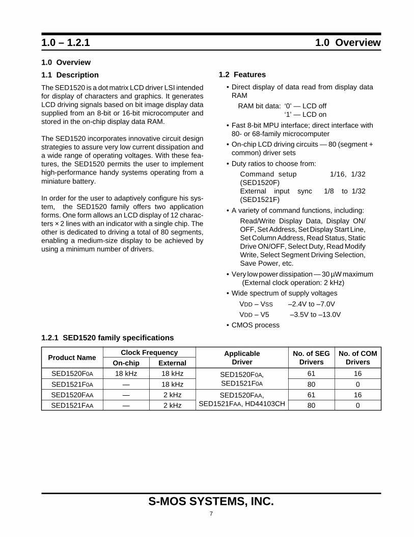
1.2.1 SED1520 family specifications
Product NameClock Frequency Applicable No. of SEG No. of COM
On-chip External Driver Drivers Drivers
SED1520F0A 18 kHz 18 kHz SED1520F0A, 61 16
SED1521F0A — 18 kHz SED1521F0A 80 0
SED1520FAA — 2 kHz 61 16
SED1521FAA — 2 kHz 80 0SED1520FAA,
SED1521FAA, HD44103CH
8
S-MOS SYSTEMS, INC.
1.0 Overview 1.3
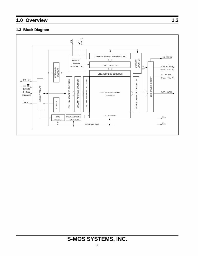
1.3 Block Diagram
LINE ADDRESS DECODER
DISPLAY DATA RAM
2560 BITS
I/O BUFFER
INTERNAL BUS
LOW ADDRESS
REGISTER
BUS
HOLDER
LINE COUNTER
DISPLAY
TIMING
GENERATOR
DISPLAY START LINE REGISTER
FR
CO
MM
AN
D
DE
CO
DE
R
CO
LUM
N A
DD
RE
SS
RE
GIS
TE
R
ST
AT
USM
PU
INT
ER
FA
CE
CO
LUM
N A
DD
RE
SS
CO
UN
TE
R
CO
LUM
N A
DD
RE
SS
DE
CO
DE
R
DIS
PLA
Y D
AT
A L
AT
CH
CIR
CU
IT
LCD
DR
IVE
R C
IRC
UIT
CO
MM
ON
CO
UN
TE
R
CL
(OS
C2)
D0 ~ D7
E , R/W
(OSC1)
RES
(RD)(WR)
VDD
VSS
V1, V4, M/S
(SG77 ~ SG79)
(SG61 ~ SG76)
SG0 ~ SG60
CM0 ~ CM15
V2, V3, V5
A0, CS
9
S-MOS SYSTEMS, INC.
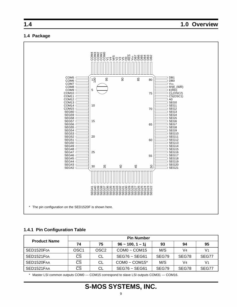
1.4.1 Pin Configuration Table
Product NamePin Number
74 75 96 ~ 100, 1 – 1j 93 94 95SED1520F0A OSC1 OSC2 COM0 ~ COM15 M/S V4 V1
SED1521F0A CS CL SEG76 ~ SEG61 SEG79 SEG78 SEG77
SED1520FAA CS CL COM0 ~ COM15* M/S V4 V1
SED1521FAA CS CL SEG76 ~ SEG61 SEG79 SEG78 SEG77
* Master LSI common outputs COM0 — COM15 correspond to slave LSI outputs COM31 — COM16.
1.4 1.0 Overview
1.4 Package
CO
M4
CO
M3
CO
M2
CO
M1
CO
M0
V1
V4
M/S
V
2 V
3 V
5 F
R
RE
S
VD
D
DB
7 D
B6
DB
5 D
B4
DB
3 D
B2
1
100
SE
G41
S
EG
40
SE
G39
S
EG
38
SE
G37
S
EG
36
SE
G35
S
EG
34
SE
G33
S
EG
32
SE
G31
S
EG
30
SE
G29
S
EG
28
SE
G27
S
EG
26
SE
G25
S
EG
24
SE
G23
S
EG
22
COM5 COM6 COM7 COM8 COM9
COM10 COM11 COM12 COM13 COM14 COM15 SEG60 SEG59 SEG58 SEG57 SEG56 SEG55 SEG54 SEG53 SEG52 SEG51 SEG50 SEG49 SEG48 SEG47 SEG46 SEG45 SEG44 SEG43 SEG42
DB1 DB0 VSS R/W, (WR) E(RD) CL(OSC2) CS(OSC1) A0 SEG0 SEG1 SEG2 SEG3 SEG4 SEG5 SEG6 SEG7 SEG8 SEG9 SEG10 SEG11 SEG12 SEG13 SEG14 SEG15 SEG16 SEG17 SEG18 SEG19 SEG20 SEG21
60
5040
55
4535
65
70
755
10
15
20
25
95 90 85
30
80
* The pin configuration on the SED1520F is shown here.

10
S-MOS SYSTEMS, INC.
THIS PAGE INTENTIONALLY BLANK
11
S-MOS SYSTEMS, INC.
2.0Pin Description

12
S-MOS SYSTEMS, INC.
THIS PAGE INTENTIONALLY BLANK
13
S-MOS SYSTEMS, INC.
2.0 – 2.3 2.0 Pin Description
2.0 Pin Description
2.1 Power Signals
• VDD
Connected to +5V power. Common to MPUpower pin VCC.
• VSS
0V, connected to system GND.
• V1 – V5
Multi-level power used to drive LCDs. Voltagespecified to each LCD cell is divided by resis-tors or impedance-converted by an operationalamplifier before being applied. Each voltage tobe applied must be based on VDD, while fulfill-ing the following conditions:
VDD ≥ V1 ≥ V2 ≥ V3 ≥ V4 ≥ V5
2.2 System Bus Interface Signals
• D7 – D0
8-bit, tri-state, bi-directional I/O bus. Normally,connected to the data bus of an 8-/16-bit stan-dard microcomputer.
• A0Input pin. Normally, the LSB of the MPU ad-dress bus is connected to this input pin toprovide data/command selection.
0 : Display control data on D0 — D7
1 : Display data on D0 — D7
• RESInput pin. The SED1520 can be reset or initial-ized by setting RES to low level (if it is inter-faced with a 68-family MPU) or high level (ifwith an 80-family MPU). This reset operationoccurs when an edge of the RES signal issensed. The level input selects the type ofinterface with the 68- or 80-family MPU:
High level : Interface with 68-family MPU
Low level : Interface with 80-family MPU
• CSChip Select input signal which is normallyobtained by decoding an address bus signal.Effective with “L” active and a chip operatingwith external clocks. For a chip containing anoscillator, CS works as an oscillation amplifierinput pin to which an oscillation resistor (Rf) isconnected. In this case, RD, WR and E must bea signal ANDed with CS.
• E (RD)• Chip interfaced with 68-family MPU:
Enable Clock signal input for the 68-family MPU.
• Chip interfaced with 80-family MPU:“L” active input pin to which the 80-familyMPU RD signal is connected. With thissignal held at “L”, the SED1520 data busworks as output.
• R/W (WR)
• Chip interface with 68-family MPU:Read/write control signal input pin.
R/W = “H” : Read
R/W = “L” : Write
• Chip interfaced with 80-family MPU:“L” active input pin to which the 80-familyWR is connected. The signal on the databus is fetched by the leading edge of WR.
2.3 LCD Drive Circuit Signals
• CL
Input signal effective with a chip using externalclocks. This display data latch signal incre-ments the line counter (at the trailing edge) orthe common counter (at the leading edge). CLis connected to CL2 of the common driver. Fora chip containing an oscillator, this pin works asthe oscillation amplifier output pin to which anoscillation resistor (Rf) is connected.

14
S-MOS SYSTEMS, INC.
2.0 Pin Description 2.3
• FR
LCD AC signal I/O pin. Connected to pin M ofthe common driver.
• I/O selection:Chip containing commons M/S = 1: Output
M/S = 0: Input
Chip containing segments alone : Input
• SEG0 – SEG79LCD column (segment) driving output. One ofthe VDD, V2, V3 and V5 levels is selected by acombination of the content of display RAM andthe FR signal.
counter and the FR signal. The common (row)scanning order for the slave LSI is reverse tothat for the master LSI.
VS V1 VDD V4
1 0
1 10 0
FR
Counter Output
Output Level
VDD V2 V5 V3
1 0
1 10 0
FR
DATA
Output Level
• COM0 – COM15 (COM31 – COM16)LCD common (row) driving output. One of theVDD, V1, V4 and V5 levels is selected by acombination of the output of the common
• M/S (SEG79)Input signal which selects the master or slaveLSI. Connected to VDD or VSS.
M/S = VDD : Master
M/S = VSS : Slave
M/S selection changes the function of pins FR,COM0 – COM15, OSC1 (CS) and OSC2 (CL):
M/S FR COM output OSC1 OSC2VDD Output COM0 – COM15 Input Output
VSS Input COM31 – COM16 NC Input
* The common scanning order for the slave driver isreverse to that for master.

15
S-MOS SYSTEMS, INC.
1.4 2.0 Pin Description
3.0Description of Circuit Blocks

16
S-MOS SYSTEMS, INC.
THIS PAGE INTENTIONALLY BLANK

17
S-MOS SYSTEMS, INC.
3.0 – 3.3 3.0 Description of Circuit Blocks
3.0 Description of Circuit Blocks
3.1 MPU Interface
3.1.1 Selection of Interface Type
The SED1520 Series uses 8 bits of bi-directional databus (D0 – D7) to transfer data. The reset pin is capableof selecting MPU interface; setting the polarity of RESto either “H” or “L” can provide direct interface of theSED1520 with a 68- or 80-family MPU (see Table 3.1below).
With CS at high level, the SED1520 is independentfrom the MPU bus and stays in standby mode. In thismode, however, the reset signal is input indepen-dently of the internal status.
Table 3.1
Polarity ofType A0 R R/W CS D0 – D7RES
“L” active 68 MPU ↑ ↑ ↑ ↑ ↑“H” active 80 MPU ↑ RD WR ↑ ↑
3.1.2 Identification of Data Bus Signals
The SED1520 uses a combination of A0, E, R/W, (RD,WR) to identify a data bus signal.
Table 3.2
Common 68 MPU 80 MPUFunction
A0 R/W RD WR
1 1 0 1 Read display data
1 0 1 0 Write display data
0 1 0 1 Read status
0 0 1 0Write to internalregister (com-mand)
3.1.3 Access to Display Data RAM andInternal Register
In order to make matching of operating frequenciesbetween the MPU and the display data RAM orinternal register, the SED1520 performs a sort of LSI-LSI pipelining via the bus holder attached to theinternal data bus. Consider the case where the MPUreads the content of the display data RAM. In the first
data read cycle (dummy), the data is stored on the busholder. In the next data read cycle, the data is readfrom the bus holder to the system bus. Also considerthe case where the MPU writes data to the displaydata RAM. In the first data write cycle, the data is heldon the bus holder. The data is written to the displaydata RAM before the next data write cycle begins.Therefore, MPU’s access to the SED1520 is affectednot by display data RAM access time (t ACC, t DS) butby cycle time (t CYC). This leads to faster transfer ofdata to and from the MPU. If the cycle time require-ment is not met, the MPU has only to execute the NOPinstruction and this is apparently equivalent to execu-tion of a waiting operation. However, there is a restric-tion on the read sequence of the display data RAM;when an address is set, its data is output not to the firstread instruction (immediately following the addresssetting operation) but to the second read instruction.Thus, one dummy read cycle is necessary after anaddress set or write cycle. This relation is shown inFigure 3.1.
3.2 Busy Flag
Busy flag being “1” means that the SED1520 isperforming its internal operation and any instructionother than Read Status is disabled. The busy flag isoutput to pin D7 by a Read Status instruction. As longas the cycle time (t CYC) requirement is met, the flagneed not be checked before each command and thisdramatically improves the MPU performance.
3.3 Display Start Line Register
This register is a pointer which determines the startline corresponding to COM0 (normally, the upper-most line of display) for display of data in the displaydata RAM. It is used for scrolling the display orchanging the page from one to another.
Executing the Set Display Start Line command sets 5bits of display start address in this register. Its contentis preset in the line counter at each timing the FRsignal changes. The line counter is incremented syn-chronously to a CL input, thus, generating a lineaddress for sequential reading of 80 bits of data fromthe display data RAM to the LCD driver circuit.

18
S-MOS SYSTEMS, INC.
Figure 3.1
3.0 Description of Circuit Blocks 3.3 – 3.5
3.4 Column Address Counter
The column address counter is a 7-bit presettablecounter which gives column addresses of the displaydata RAM as shown in Figure 3.3. When a Read/WriteDisplay Data command comes in, the counter isincremented by 1. For any nonexisting address over50H, the counter is locked and not incremented.
The column address counter is independent from thepage register.
3.5 Page Register
This register gives a page address of the display dataRAM as shown in Figure 3.3. The Set Page Addresscommand permits the MPU to access a new page ofthe display data RAM.
N
WR
DATA
Bus
Holder
WR
MPU
Internal Timing
N N+1 N+2 N+3
N+1 N+2 N+3
Write
Read
N N n n+1
Address set at N
Dummy read Data read at N
Data read at N+1
N+2N+1N
N n n+1 n+2
WR
RD
DATA
WR
RD
Column Address
Bus
Holder
MPU
Internal Timing

19
S-MOS SYSTEMS, INC.
3.6 – 3.11 3.0 Description of Circuit Blocks
3.6 Display Data RAM
Dot data for display is stored in this RAM. Since theMPU and LCD driver circuit operate independently ofeach other, data can be changed asynchronouslywithout adverse effect on the display.
One bit of the display data RAM is assigned to one bitof LCD:
LCD on = “1”
LCD off = “0”
The ADC command inverts the assignment relation-ship between a display data RAM column addressand a segment output (see Figure 3.3).
3.7 Common Timing Generator
This circuit generates common timing and frame (FR)signals from the basic clock (CL). The Select Dutycommand selects a duty of 1/16 or 1/32. The 1/32 dutyis achieved by a two-chip (master and slave) configu-ration (common multi-chip system).
3.8 Display Data Latch Circuit
The display data latch circuit temporarily stores thedata which will be output from the display data RAMto the LCD driver circuit at one-common intervals. TheDisplay ON/OFF and Static Driver ON/OFF com-mands control the latched data so that the data in thedisplay data RAM remains unchanged.
3.9 LCD Driver Circuit
This circuit generates 80 sets of multiplexer thatgenerate quartet levels for LCD driving. Display datain the display data latch, common timing generatoroutput and FR signal are combined to output an LCDdriving waveform.
3.10 Display Timing Generator
This circuit generates an internal display timing signalfrom the basic clock (CL) and frame signal (FR).
The frame signal FR makes the LCD driver circuitgenerate a dual frame AC driving waveform (type B)to drive LCD, while making both the line counter andcommon timing generator synchronized to the FRsignal output LSI (dedicated common driver or theSED1520 master LSI). To achieve these functions,the FR signal must be a clock with a duty of 50% whichis synchronized to the frame period. The clock CL isa clock used to operate the line counter. For a systemin which both the SED1520 and SED1521F coexist,they should be of LSI types having the same clockfrequency to be applied to pin CL.
3.11 Oscillation Circuit
This circuit is a low-power CR oscillator which uses anoscillation resistor Rf alone to adjust the oscillationfrequency. It generates display timing signals. TheSED1520 is available in two LSI types if classified byoscillation: one LSI type contains an oscillation circuitand the other uses an externally provided clock.
Figure 3.2
0 1 2 1514 0 1 15
16 17 30 16 17 3131
FR (Master Output)
Master
Common
Slave Common

20
S-MOS SYSTEMS, INC.
3.0 Description of Circuit Blocks 3.6 – 3.11
Figure 3.3. Relationship between Display Data RAM Locations and Addresses (Display Start Line: 08)
Page
addressD
AT
ALine
addressC
omm
on output
D0
D1
D2
D3
D4
D5
D6
D7
D0
D1
D2
D3
D4
D5
D6
D7
D0
D1
D2
D3
D4
D5
D6
D7
D0
D1
D2
D3
D4
D5
D6
D7
D
1,D2=
0,0
0,1
1,0
1,1
00H
01 02 03 04 05 06 07 08 09 0A
0B
0C
0D
0E
0F
10 11 12 13 14 15 16 17 18 19 1A
1B
1C
1D
1E
1F
4D 4E 4F
02 01 00
SEG77 SEG78 SEG79
00H 01 02 03 04 05 06 07
4F 4E 4D 4C 4B 4A 49 48
SEG0 SEG1 SEG2 SEG3 SEG4 SEG5 SEG6 SEG7
D0 = 0
ADCSEG Pin
CO
M 0
CO
M 1
CO
M 2
CO
M 3
CO
M 4
CO
M 5
CO
M 6
CO
M 7
CO
M 8
CO
M 9
CO
M10
CO
M11
CO
M12
CO
M13
CO
M14
CO
M15
CO
M16
CO
M17
CO
M18
CO
M19
CO
M20
CO
M21
CO
M22
CO
M23
CO
M24
CO
M25
CO
M26
CO
M27
CO
M28
CO
M29
CO
M30
CO
M31
Page 0
P
age 1
Page 2
P
age 3
Start
1/16
Associated
Line (ex.)
Assignm
ent
(In this example,
the display start line is set at address 08.) Display Area
D0 = 1
Column Address

21
S-MOS SYSTEMS, INC.
3.6 – 3.11 3.0 Description of Circuit Blocks
Figure 3.4. LSI containing oscillator
M/S(CS)
OSC1(CL)
OSC2
Master LSIVDD
M/S(CS)
OSC1(CL)
OSC2
Slave LSI
VDD
Rf *2
*1
Open
*1 *2
As the parasitic capacitance in this portion increases, the oscillation frequency will shift to a lower level. The Rf must have a smaller value than the specification. For a system having two or more slave LSIs, a CMOS buffer is necessary.
CL2
Y–Driver
CL
SED1521FAA
Figure 3.5. LSI operating with external clock

22
S-MOS SYSTEMS, INC.
The input at pin RES is level-sensed to select an MPUinterface mode as shown in Table 3.1. For interfacingwith an 80-family MPU, an “H” active reset signal isinput to pin RES. For interfacing with a 68-familyMPU, an “L” active reset signal is input to the pin (seeFigure 6.1).
As exemplified in chapter 6.0, “Interface with MPU,”pin RES is connected to the MPU reset pin. Thus, theSED1520 and the MPU are initialized at the sametime. If system is initialized by pin RES at power-on,it may no longer be reset.
The Reset command causes initialization (b), (d) and(e).
3.0 Description of Circuit Blocks 3.11 – 3.12
The oscillation resistor Rf is connected as shownbelow. Where an LSI containing an oscillation circuitis operated with an external clock, it is necessary toinput the clock with the same phase as OSC2 of themaster LSI to OSC2 of the slave LSI.
3.12 Reset Circuit
This circuit senses the leading edge or trailing edge ofRES and initializes the system when its power isswitched on.
Initialization:(a) Display off
(b) Display start line register: First line
(c) Static drive off
(d) Column address counter: Address 0
(e) Page address register: Page 0
(f) Select duty: 1/32
(g) Select ADC: Forward (ADC commandD0 = “0”, ADC status flag = “1”)
(h) Read modify write off

23
S-MOS SYSTEMS, INC.
3.11 – 3.12 3.0 Description of Circuit Blocks
Figure 3.6. Examples of LCD Driving Waveform
VDD VSS
VDD V1 V2 V3 V4 V5
FR
COM 0
VDD V1 V2 V3 V4 V5
COM 1
VDD V1 V2 V3 V4 V5
COM 2
VDD V1 V2 V3 V4 V5
SEG 0
VDD V1 V2 V3 V4 V5
SEG 1
V5 V4 V3 V2 V1 VDD –V1 –V2 –V3 –V4 –V5
COM 0 – SEG 0
V5 V4 V3 V2 V1 VDD –V1 –V2 –V3 –V4 –V5
COM 0 – SEG 1
COM 0
1
2
3
4
5
6
7
8
9
10
11
12
13
14
15
SE
G 0
1 2 3 4
0 1 2 3 15 0 1 2 3 15
0 1 2 3 31 0 1 2 3 31

24
S-MOS SYSTEMS, INC.
THIS PAGE INTENTIONALLY BLANK

25
S-MOS SYSTEMS, INC.
4.0Commands

26
S-MOS SYSTEMS, INC.
THIS PAGE INTENTIONALLY BLANK

27
S-MOS SYSTEMS, INC.
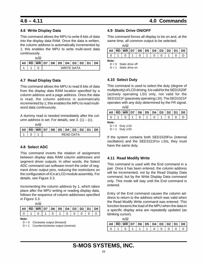
Table 4.1. Commands
CommandCode
FunctionA0 RD WR D7 D6 D5 D4 D3 D2 D1 D0
(1) Display ON/OFF 0 1 0 1 0 1 0 1 1 1 0/1 Turns all display on or off, independently ofdisplay RAM data or internal status.
1: ON0: OFF (Power-saving mode with static drive on)*
(2) Display Start Line 0 1 0 1 1 0 Specifies RAM line corresponding to uppermostline (COM0) of display.
(3) Set Page Address 0 1 0 1 0 1 1 1 0 Page (0–3) Sets display RAM page in page address register.
(4) 0 1 0 0 Column Address (0–79) Sets display RAM column address in columnaddress register.
(5) Read Status 0 0 1 0 0 0 0 Reads the following status:
BUSY 1: Internal operation 0: ReadyADC 1: CW output (forward)
0: CCW output (reverse)ON/OFF 1: Display off 0: Display onRESET 1: Being reset 0: Normal
(6) Write Display Data 1 1 0 Write Data Writes data from databus into display RAM.
(7) Read Display Data 1 0 1 Read Data Reads data fromdisplay RAM ontodata bus.
(8) Select ADC 0 1 0 1 0 1 0 0 0 0 0/1 Used to invert relationship of assignmentbetween display RAM column addresses andsegment driver outputs.
0: CW output (forward)1: CCW output (reverse)
(9) Static Drive ON/OFF 0 1 0 1 0 1 0 0 1 0 0/1 Selects normal display or static driving operation.
1: Static drive (power-saving mode)0: Normal driving
(10) Select Duty 0 1 0 1 0 1 0 1 0 0 0/1 Selects LCD cell driving duty
1: 1/320: 1/16
(11) Read Modify Write 0 1 0 1 1 1 0 0 0 0 0 Increments column address counter by 1 whendisplay data is written. (This is not done whendata is read.)
(12) End 0 1 0 1 1 1 0 1 1 1 0 Clears read modify write mode.
(13) Reset 0 1 0 1 1 1 0 0 0 1 0 Sets display start line register on the first line.Also sets column address counter and pageaddress counter to 0.
* With display off (command (1)), static drive going on (9) invokes power-saving mode.
4.0 4.0 Commands
4.0 Commands
Table 4.1 lists the commands used with the SED1520.This LSI uses a combination of A0, R/W, (RD, WR) toidentify a data bus signal. Interpretation and execu-
tion of a command depends not on external clock buton internal timing alone. Therefore, a command canbe executed so fast that no busy check is needed.
Set Column (Segment)Address
Display StartAddress (0 – 31)
Bus
y
AD
C
ON
/OF
F
RE
SE
T
A detailed description of all the commands follows.
Display RAM locationwhose address has beenpreset is accessed. Afteraccess, the column ad-dress is incremented by 1.

28
S-MOS SYSTEMS, INC.
4.0 Commands 4.1 – 4.5
4.1 Display ON/OFF
This command forces all display to turn on or off.R/W
A0 RD WR D7 D6 D5 D4 D3 D2 D1 D0
0 1 0 1 0 1 0 1 1 1 D
Note:D = 0 Display OFFD = 1 Display ON
4.2 Display Start Line
This command specifies a line address (shown inFigure 3.3) thus marking the display line that corre-sponds to COM0. Display begins with the specifiedline address and covers as many lines as match thedisplay duty in address ascending order. Dynamicline address change with the Display Start Line com-mand enables column-wise scrolling or page change.
R/W
A0 RD WR D7 D6 D5 D4 D3 D2 D1 D0
0 1 0 1 1 0 A4 A3 A2 A1 A0
← High order bits
A4 A3 A2 A1 A0 Line Address
0 0 0 0 0 0
0 0 0 0 1 1
↓ ↓1 1 1 1 1 31
4.3 Set Page Address
This command is used to specify a page addressequivalent to a row address for MPU access to thedisplay data RAM. A required bit of the display dataRAM can be accessed by specifying its page addressand column address. Changing the page addresscauses no change in display.
R/W
A0 RD WR D7 D6 D5 D4 D3 D2 D1 D0
0 1 0 1 0 1 1 1 0 A1 A0
4.4 Column Address
This command specifies a display data RAM columnaddress. The column address is incremented by 1each time the MPU accesses from the set address tothe display data RAM. Thus it is possible for the MPUto gain continuous access to only the data. Thisincrementing stops with address 80; the page ad-dress is not continuously changed.
R/W
A0 RD WR D7 D6 D5 D4 D3 D2 D1 D0
0 1 0 0 A6 A5 A4 A3 A2 A1 A0
A6 A5 A4 A3 A2 A1 A0ColumnAddress
0 0 0 0 0 0 0 0
0 0 0 0 0 0 1 1
↓ ↓1 0 0 1 1 1 1 79
4.5 Read Status
R/W
A0 RD WR D7 D6 D5 D4 D3 D2 D1 D0
0 0 1 BUSY ADC RESET 0 0 0 0
Note:
BUSY BUSY being “1” means that system is performingan internal operation or is reset. No command isaccepted before BUSY = “0”. As long as the cycletime requirement is met, no BUSY check is needed.
ADC Indicates assignment of column addresses tosegment drivers.
0 : Inverted (column address 79 – n ↔ seg-ment driver n)
1 : Forward (column address n ↔ segmentdriver n)
ON/OFF Indicates display on or off.
0 : Display on
1 : Display off
This bit has polarity reverse to the Display ON/OFF command.
RESET Indicates that system is being initialized by theRES signal or the Reset command.
0 : Display mode
1 : Being reset
ON /OFF
A1 A0 Page
0 0 0
0 1 1
A1 A0 Page
1 0 2
1 1 3
29
S-MOS SYSTEMS, INC.
4.6 – 4.11 4.0 Commands
4.6 Write Display Data
This command allows the MPU to write 8 bits of datainto the display data RAM. Once the data is written,the column address is automatically incremented by1; this enables the MPU to write multi-word datacontinuously.
R/W
A0 RD WR D7 D6 D5 D4 D3 D2 D1 D0
1 1 0 WRITE DATA
4.7 Read Display Data
This command allows the MPU to read 8 bits of datafrom the display data RAM location specified by acolumn address and a page address. Once the datais read, the column address is automaticallyincremented by 1; this enables the MPU to read multi-word data continuously.
A dummy read is needed immediately after the col-umn address is set. For details, see 3. (1) – (c).
R/W
A0 RD WR D7 D6 D5 D4 D3 D2 D1 D0
1 0 1 READ DATA
4.8 Select ADC
This command inverts the relation of assignmentbetween display data RAM column addresses andsegment driver outputs. In other words, the SelectADC command can software-invert the order of seg-ment driver output pins, reducing the restrictions onthe configuration of ICs at LCD module assembly. Fordetails, see Figure 3.3.
Incrementing the column address by 1, which takesplace after the MPU writing or reading display data,follows the sequence of column addresses specifiedin Figure 3.3.
R/W
A0 RD WR D7 D6 D5 D4 D3 D2 D1 D0
0 1 0 1 0 1 0 0 0 0 0
Note:D = 0 Clockwise output (forward)D = 1 Counterclockwise output (reverse)
4.9 Static Drive ON/OFF
This command forces all display to be on and, at thesame time, all common output to be selected.
R/W
A0 RD WR D7 D6 D5 D4 D3 D2 D1 D0
0 1 0 1 0 1 0 0 1 0 D
Note:D = 0 Static drive offD = 1 Static drive on
4.10 Select Duty
This command is used to select the duty (degree ofmultiplexity) of LCD driving. It is valid for the SED1520F(actively operating LSI) only, not valid for theSED1521F (passively operating LSI). The SED1521Foperates with any duty determined by the FR signal.
R/W
A0 RD WR D7 D6 D5 D4 D3 D2 D1 D0
0 1 0 1 0 1 0 1 0 0 D
Note:D = 0 Duty 1/16D = 1 Duty 1/32
If the system contains both SED1520F0A (internaloscillation) and the SED1521F0A LSIs, they musthave the same duty.
4.11 Read Modify Write
This command is used with the End command in apair. Once it has been entered, the column addresswill be incremented, not by the Read Display Datacommand, but by the Write Display Data commandonly. This mode will stay until the End command isentered.
Entry of the End command causes the column ad-dress to return to the address which was valid whenthe Read Modify Write command was entered. Thisfunction lessens the load of the MPU when the data ina specific display area are repeatedly updated (asblinking cursor).
R/W
A0 RD WR D7 D6 D5 D4 D3 D2 D1 D0
0 1 0 1 1 1 0 0 0 0 0

30
S-MOS SYSTEMS, INC.
* Even in the Read Modify Write mode, any commandother than Read/Write Data and Set Column Addressmay be used.
4.0 Commands 4.11 – 4.14
Page Address Set
Column Address Set
Read–Modify–Write Cycle
Dummy Read
Data Read
Data Write
Changes Finished?
END
No
Figure 4.1. Cursor blinking sequence
4.12 End
This command cancels the Read Modify Write com-mand, returning the column address to the initialmode address. See Figure 4.2.
R/W
A0 RD WR D7 D6 D5 D4 D3 D2 D1 D0
0 1 0 1 1 1 0 1 1 1 0
4.13 Reset
This command initializes the display start line regis-ter, column address counter, and page address counterwithout any effect on the display data RAM. Fordetails, see 6-(12).
The reset operation follows entry of the Reset com-mand.
R/W
A0 RD WR D7 D6 D5 D4 D3 D2 D1 D0
0 1 0 1 1 1 0 0 0 1 0
Initialization at power-on is performed, not by theReset command, but by a reset signal applied to theRES pin.
4.14 Save Power (Combined Command)
Static drive going on with display off invokes power-saving mode, reducing current consumption to nearlystatic current level. During this mode, the SED1520holds the following conditions:
• It stops driving the LCD; the segment andcommon driver outputs are at VDD level.
• Oscillation and external clock input are dis-abled; OSC2 is in floating condition.
• The display data and operational mode areheld.
The power-saving mode is cancelled by display on orstatic drive off.
If an external resistor division circuit is used to giveLCD driving voltage level, the current flowing into theresistors must be cut off by the power-save signal.
Figure 4.2
N N+1 N+2 N+m NReturn
EndRead modify write mode set
Column Address

31
S-MOS SYSTEMS, INC.
4.14 4.0 Commands
VDD
V1
V2
V3
V4
V5
VDD
VSSH
Power save signal
SED1520
Figure 4.3

32
S-MOS SYSTEMS, INC.
THIS PAGE INTENTIONALLY BLANK
33
S-MOS SYSTEMS, INC.
5.0Electrical Characteristics

34
S-MOS SYSTEMS, INC.
THIS PAGE INTENTIONALLY BLANK
35
S-MOS SYSTEMS, INC.
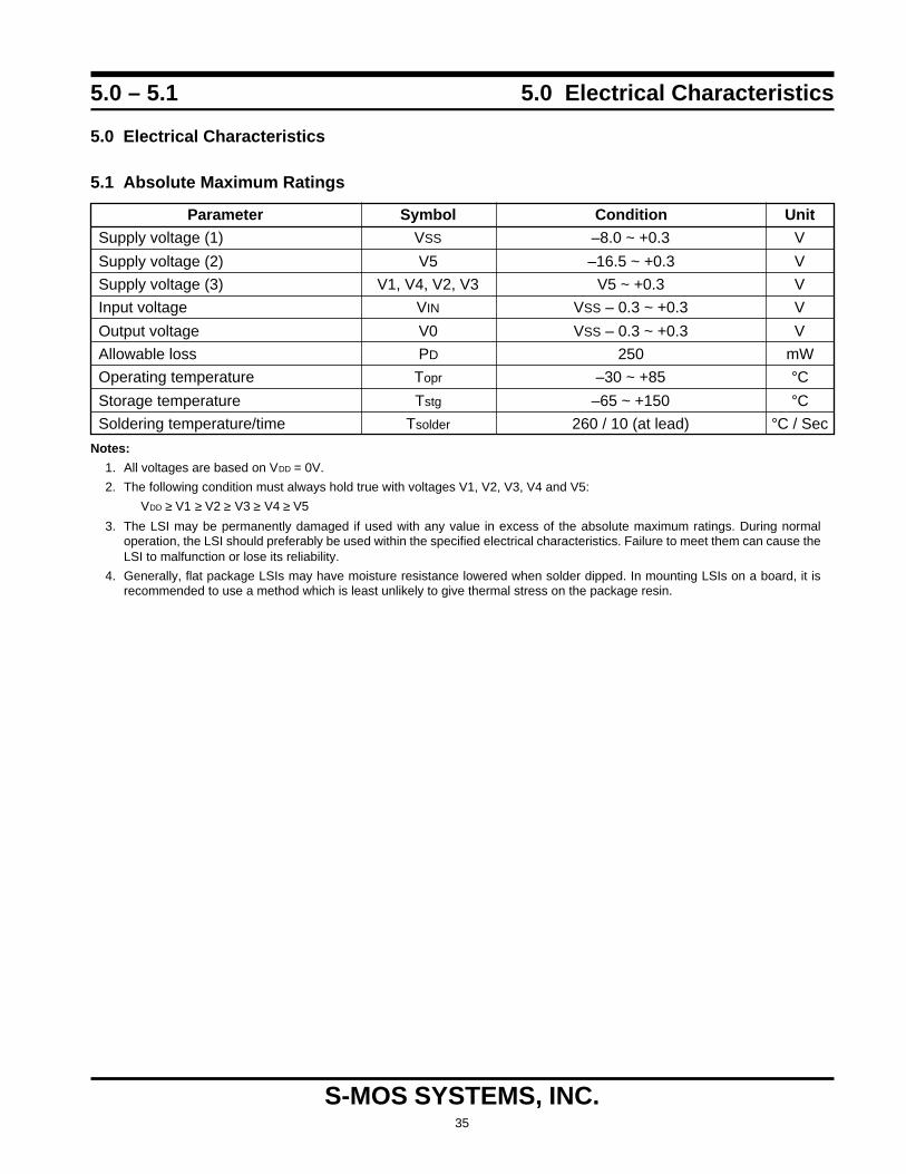
5.0 – 5.1 5.0 Electrical Characteristics
5.0 Electrical Characteristics
5.1 Absolute Maximum Ratings
Parameter Symbol Condition UnitSupply voltage (1) VSS –8.0 ~ +0.3 V
Supply voltage (2) V5 –16.5 ~ +0.3 V
Supply voltage (3) V1, V4, V2, V3 V5 ~ +0.3 V
Input voltage VIN VSS – 0.3 ~ +0.3 V
Output voltage V0 VSS – 0.3 ~ +0.3 V
Allowable loss PD 250 mW
Operating temperature Topr –30 ~ +85 °CStorage temperature Tstg –65 ~ +150 °CSoldering temperature/time Tsolder 260 / 10 (at lead) °C / Sec
Notes:
1. All voltages are based on VDD = 0V.
2. The following condition must always hold true with voltages V1, V2, V3, V4 and V5:
VDD ≥ V1 ≥ V2 ≥ V3 ≥ V4 ≥ V5
3. The LSI may be permanently damaged if used with any value in excess of the absolute maximum ratings. During normaloperation, the LSI should preferably be used within the specified electrical characteristics. Failure to meet them can cause theLSI to malfunction or lose its reliability.
4. Generally, flat package LSIs may have moisture resistance lowered when solder dipped. In mounting LSIs on a board, it isrecommended to use a method which is least unlikely to give thermal stress on the package resin.
36
S-MOS SYSTEMS, INC.
5.0 Electrical Characteristics 5.2
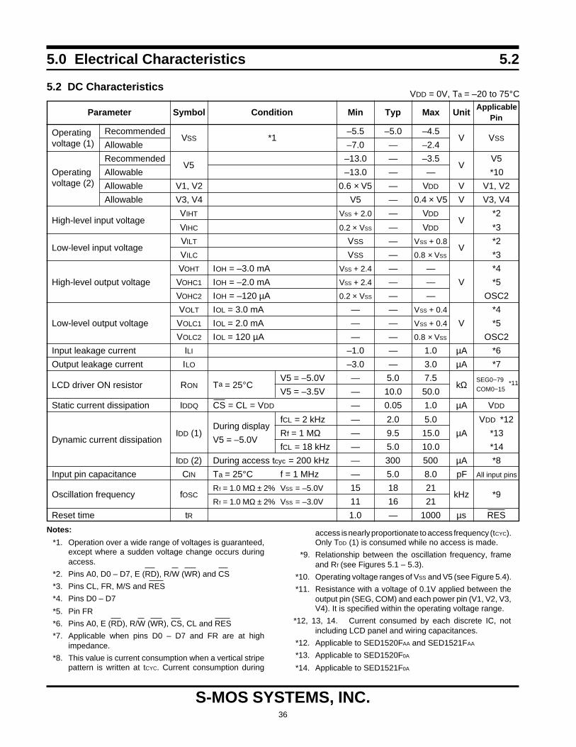
5.2 DC CharacteristicsVDD = 0V, Ta = –20 to 75°C
Parameter Symbol Condition Min Typ Max UnitApplicable
Pin
RecommendedVSS *1
–5.5 –5.0 –4.5V VSS
Allowable –7.0 — –2.4
RecommendedV5
–13.0 — –3.5V
V5
Allowable –13.0 — — *10
Allowable V1, V2 0.6 × V5 — VDD V V1, V2
Allowable V3, V4 V5 — 0.4 × V5 V V3, V4
High-level input voltageVIHT VSS + 2.0 — VDD
V*2
VIHC 0.2 × VSS — VDD *3
Low-level input voltageVILT VSS — VSS + 0.8
V*2
VILC VSS — 0.8 × VSS *3
VOHT IOH = –3.0 mA VSS + 2.4 — — *4
High-level output voltage VOHC1 IOH = –2.0 mA VSS + 2.4 — — V *5
VOHC2 IOH = –120 µA 0.2 × VSS — — OSC2
VOLT IOL = 3.0 mA — — VSS + 0.4 *4
Low-level output voltage VOLC1 IOL = 2.0 mA — — VSS + 0.4 V *5
VOLC2 IOL = 120 µA — — 0.8 × VSS OSC2
Input leakage current ILI –1.0 — 1.0 µA *6
Output leakage current ILO –3.0 — 3.0 µA *7
LCD driver ON resistor RON Ta = 25°CV5 = –5.0V — 5.0 7.5
kΩV5 = –3.5V — 10.0 50.0
Static current dissipation IDDQ CS = CL = VDD — 0.05 1.0 µA VDD
During displayfCL = 2 kHz — 2.0 5.0 VDD *12
Dynamic current dissipationIDD (1)
V5 = –5.0VRf = 1 MΩ — 9.5 15.0 µA *13
fCL = 18 kHz — 5.0 10.0 *14
IDD (2) During access tcyc = 200 kHz — 300 500 µA *8
Input pin capacitance CIN Ta = 25°C f = 1 MHz — 5.0 8.0 pF All input pins
Oscillation frequency fOSCRf = 1.0 MΩ ± 2% VSS = –5.0V 15 18 21
kHz *9Rf = 1.0 MΩ ± 2% VSS = –3.0V 11 16 21
Reset time tR 1.0 — 1000 µs RES
Operatingvoltage (1)
Operatingvoltage (2)
SEG0~79 *11COM0~15
Notes:
*1. Operation over a wide range of voltages is guaranteed,except where a sudden voltage change occurs duringaccess.
*2. Pins A0, D0 – D7, E (RD), R/W (WR) and CS
*3. Pins CL, FR, M/S and RES
*4. Pins D0 – D7
*5. Pin FR
*6. Pins A0, E (RD), R/W (WR), CS, CL and RES
*7. Applicable when pins D0 – D7 and FR are at highimpedance.
*8. This value is current consumption when a vertical stripepattern is written at tCYC. Current consumption during
access is nearly proportionate to access frequency (tCYC).Only TDD (1) is consumed while no access is made.
*9. Relationship between the oscillation frequency, frameand Rf (see Figures 5.1 – 5.3).
*10. Operating voltage ranges of VSS and V5 (see Figure 5.4).
*11. Resistance with a voltage of 0.1V applied between theoutput pin (SEG, COM) and each power pin (V1, V2, V3,V4). It is specified within the operating voltage range.
*12, 13, 14. Current consumed by each discrete IC, notincluding LCD panel and wiring capacitances.
*12. Applicable to SED1520FAA and SED1521FAA
*13. Applicable to SED1520F0A
*14. Applicable to SED1521F0A

37
S-MOS SYSTEMS, INC.
5.2 5.0 Electrical Characteristics
*9 Relation between oscillation frequency, frame and Rf [SED1520F0A]
Figure 5.1 Figure 5.2
Relationship between external clock (fCL) and frame [SED1520FAA]
0 1 2 3
100
200
CLf (KHz)
Fra
me
(Hz)
Duty 1/32 Duty 1/16
Figure 5.3
*10 Operating voltage range of VSS and V5
-15
-10
-5
0 -2 -4 -6 -8
SSV (V)
V 5(V
)
Operating Voltage Range
Figure 5.4
(M )Ω
0 0.5 1.0 1.5 2.0 2.5
10
20
30
40
f
SS
R
f OS
C(K
Hz)
Ta = 25°C V = -5VfR
OSC1
OSC2
0 0.5 1.0 1.5 2.0 2.5
100
200
f
SS
R (M )
Fra
me
(Hz)
Duty 1/16, 1/32 Ta = 25°C V = -5V
Ω

38
S-MOS SYSTEMS, INC.
5.0 Electrical Characteristics 5.3 – 5.3.1
5.3 Timing Characteristics
5.3.1 System Bus Read/Write I (80-family MPU)Ta = –20 to 75°C, VSS = –5.0V ±10%
Parameter Symbol Signal Condition Min Typ Max UnitAddress hold time tAH8
A0, CS10 — — ns
Address setup time tAW8 20 — — ns
System cycle time tCYC8WR, RD
1000 — — ns
Control pulse width tCC 200 — — ns
Data setup time tDS8 80 — — ns
Data hold time tDH8D0 – D7
10 — — ns
RD access time tACC8CL = 100 pF
— — 90 ns
Output disable time tOH8 10 — 60 ns
*1 Each of the values where VSS = –3.0V is about 200% of that where VSS = –5.0V (i.e., the listed value).
*2 The rise or fall time of input signals should be less than 15 ns.
tAW8tCYC8
tCC
tDS8
tOH8tACC8
tDH8
A0, CS
WR, RD
D0 ~ D7 (WRITE)
D0 ~ D7 (READ)
tAH8
Figure 5.5. System bus read/write I (80-family MPU)

39
S-MOS SYSTEMS, INC.
5.3.2 5.0 Electrical Characteristics
5.3.2 System Bus Read/Write II (68-family MPU)Ta = –210 to 75°C, VSS = –5.0V ±10%
Parameter Symbol Signal Condition Min Typ Max Unit
System cycle time tCYC6 *1 A0, CS 1000 — — ns
Address setup time tAW6R/W
20 — — ns
Address hold time tAH6 10 — — ns
Data setup time tDS6 80 — — ns
Data hold time tDH6D0 – D7
10 — — ns
Output disable time tOH6CL = 100 pF
10 — 60 ns
Access time tACC6 — — 90 ns
Enable pulse width: ReadtEW E
100 — — ns
Enable pulse width: Write 80 — — ns
*1 tCYC6 indicates the cycle time during which CS•E = “H”. It does not mean the cycle time of signal E.
*2 Each of the values where VSS = –3.0V is about 200% of that where VSS = –5.0V (i.e., the listed value).
*3 The rise or fall time of input signals should be less than 15 ns.
tDS6
tEW
tCYC6
tAW6
tAH6
tDH6
tOH6tACC6
A0, CS
R / W
D0 ~ D7 (WRITE)
D0 ~ D7 (READ)
E
Figure 5.6. System bus read/write II (68-family MPU)

40
S-MOS SYSTEMS, INC.
5.0 Electrical Characteristics 5.3.3
5.3.3 Display Control Timing
Input TimingTa = –20 to 75°C, VSS = –5.0V ±10%
Parameter Symbol Signal Condition Min Typ Max UnitLow level pulse width tWLCL 35 — — µs
High level pulse width tWHCLCL
35 — — µs
Rise time tr — 30 150 ns
Fall time tf — 30 150 ns
FR delay time tDFR FR –2.0 0.2 2.0 µs
Output TimingTa = –20 to 75°C, VSS = –5.0V ±10%
Parameter Symbol Signal Condition Min Typ Max Unit
FR delay time tDFR FR CL = 100 pF — 0.2 0.4 µs
*1. The listed FR input delay time applies to the SED1521 and 1520 (slave).
The listed FR output delay time applies to the SED1520 (master).
*2. Each of the values where VSS = –3.0V is about 200% of that where VSS = –5.0V (i.e., the listed value).
tWLCL
tWHCL
tDFR
tf tr
CL
FR
Figure 5.7. Display control timing
41
S-MOS SYSTEMS, INC.
6.0MPU Interface
(Reference)

42
S-MOS SYSTEMS, INC.
THIS PAGE INTENTIONALLY BLANK

43
S-MOS SYSTEMS, INC.
6.0 6.0 MPU Interface (Reference)
6.0 MPU Interface (Reference)
A0
IORQ
RD
WR
RESGND
RESET
CS
RD
WR
RES
MPU SED1520FAA
Decoder
VSS
A2 ~ A7
D0 ~ D7D0 ~ D7
VS
VDDVCC A0
Figure 6.1. 80-family MPU
Figure 6.2. 68-family MPU
A0
VMA
E
R/W
RESGND
RESET
CS
E
R/W
RES
MPU SED1520FAA
Decoder
VSS
A0 ~ A13
D0 ~ D7D0 ~ D7
VS
VDDVCC A0
* These examples also apply to the SED1521F0A/SED1521FAA.
* The SED1520F0A (containing an oscillator) does nothave pin CS. The output ORed with CS must be appliedto pins A0, RD (E) and WR (R/W).

44
S-MOS SYSTEMS, INC.
SED1520FOADecoderA0 D0 ~ D7 RD(E) WR(R/W) RES
CS
Figure 6.3
6.0 MPU Interface (Reference) 6.0
45
S-MOS SYSTEMS, INC.
7.0LCD Driver
Interconnections

46
S-MOS SYSTEMS, INC.
THIS PAGE INTENTIONALLY BLANK

47
S-MOS SYSTEMS, INC.
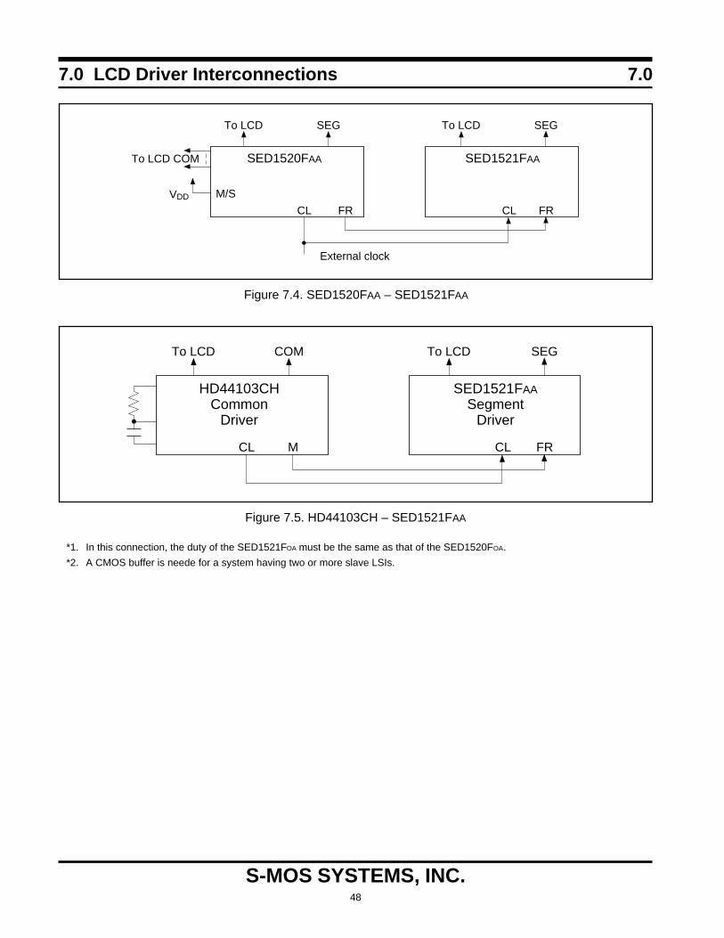
7.0 7.0 LCD Driver Interconnections
7.0 LCD Driver Interconnections
Figure 7.1. SED1520FOA – SED1520FOA
To LCD SEG
M/S
SED1520FAA (Slave)
VDD VSSM/S
SED1520FAA (Master)
CL FR CL FR
To LCD SEG
To LCD COMTo LCD COM
External clock
Figure 7.2. SED1520FAA – SED1520FAA
To LCD SEG
SED1521FOA
OSC1
Rf
VDD M/S
SED1520FOA
OSC2 FR OSC1 OSC2 FR
To LCD SEG
To LCD COM
*2
Figure 7.3 SED1520FOA – SED1521FOA *1
*1. In this connection, the duty of the SED1521FOA must be the same as that of the SED1520FOA.
*2. A CMOS buffer is neede for a system having two or more slave LSIs.
To LCD SEG
M/S
SED1520FOA (Slave)
OSC1
Rf
VDD VSSM/S
SED1520FOA (Master)
OSC2 FR OSC1 OSC2 FR
To LCD SEG
To LCD COMTo LCD COM
48
S-MOS SYSTEMS, INC.
Figure 7.4. SED1520FAA – SED1521FAA
Figure 7.5. HD44103CH – SED1521FAA
7.0 LCD Driver Interconnections 7.0
*1. In this connection, the duty of the SED1521FOA must be the same as that of the SED1520FOA.
*2. A CMOS buffer is neede for a system having two or more slave LSIs.
To LCD SEG
SED1521FAA
VDD M/S
SED1520FAA
CL FR CL FR
To LCD SEG
To LCD COM
External clock
To LCD COM
SED1521FAA Segment
Driver
HD44103CH Common
Driver
CL M CL FR
To LCD SEG
49
S-MOS SYSTEMS, INC.
8.0Typical Connections
with LCD Panel

50
S-MOS SYSTEMS, INC.
THIS PAGE INTENTIONALLY BLANK
51
S-MOS SYSTEMS, INC.
8.0 8.0 Typical Connections with LCD Panel
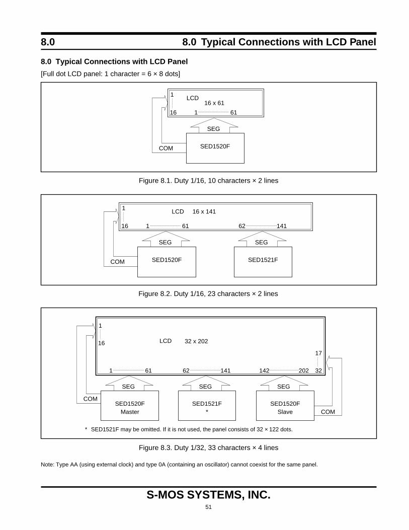
8.0 Typical Connections with LCD Panel
[Full dot LCD panel: 1 character = 6 × 8 dots]
SEG
SED1520F
16 x 61LCD1
16 1 61
COM
Figure 8.1. Duty 1/16, 10 characters × 2 lines
SEG
SED1520F
16 x 141LCD1
16 1 61
SEG
SED1521F
62 141
COM
Figure 8.2. Duty 1/16, 23 characters × 2 lines
SEG
SED1520FMaster
32 x 202LCD
1
16
1 61
17
32
SEG
SED1521F*
62 141
COM
COM
SEG
SED1520FSlave
142 202
* SED1521F may be omitted. If it is not used, the panel consists of 32 × 122 dots.
Figure 8.3. Duty 1/32, 33 characters × 4 lines
Note: Type AA (using external clock) and type 0A (containing an oscillator) cannot coexist for the same panel.

52
S-MOS SYSTEMS, INC.
8.0 Typical Connections with LCD Panel 8.0
SEG
32 x 320LCD1
32 1 80
SED1521FAA (1)
SEG
SED1521FAA (2)
SEG
SED1521FAA (3)
SEG
SED1521FAA (4)
81 160 161 240 241 320HD
4410
3CH
CO
M
Figure 8.4. Duty 1/32, 20 kanji characters × 2 lines (kanji character 16 × 16 dots)
SEG
64 x 320LCD
33
641 80
SED1521FAA (1)
SEG
SED1521FAA (2)
SEG
SED1521FAA (3)
SEG
SED1521FAA (4)
81 160 161 240 241 320
SEG SEG SEG SEG
(5) SED1521FAA
(6) SED1521FAA
(7) SED1521FAA
(8) SED1521FAA
1
32
HD
4410
3CH
CO
MC
OM
Figure 8.5. Duty 1/32, 2-screen display, 20 kanji characters × 4 lines
53
S-MOS SYSTEMS, INC.
9.0Package Dimensions
(Reference)

54
S-MOS SYSTEMS, INC.
THIS PAGE INTENTIONALLY BLANK

55
S-MOS SYSTEMS, INC.
9.0 9.0 Package Dimensions (Reference)
9.0 Package Dimensions (Reference)
19
.6 ±
Index
81
100
50
31
1 30
80 51
25.6 ± 0.4
20
0.65
0.30
0.4
14
1.5 ± 0.3
0.
15±
0.05
2.
7 ±
0.1
0 – 12°
2.8
Figure 9.1. Package Dimensions

56
S-MOS SYSTEMS, INC.
THIS PAGE INTENTIONALLY BLANK