section 43. high-speed pwm · 2013-06-08 · • sphasex: pwm secondary phase shift register -...
TRANSCRIPT

Section 43. High-Speed PWM
High-Speed PW
M
43
HIGHLIGHTSThis section of the manual contains the following major topics:
43.1 Introduction .................................................................................................................. 43-243.2 Features....................................................................................................................... 43-243.3 Control Registers ......................................................................................................... 43-343.4 Architecture Overview................................................................................................ 43-3243.5 Module Description .................................................................................................... 43-3543.6 PWM Generator ......................................................................................................... 43-4543.7 PWM Triggers ............................................................................................................ 43-5743.8 PWM Interrupts .......................................................................................................... 43-6443.9 PWM Operating Modes.............................................................................................. 43-6543.10 PWM Fault Pins ......................................................................................................... 43-7043.11 Special Features ........................................................................................................ 43-8243.12 PWM Output Pin Control............................................................................................ 43-8843.13 Immediate Update of PWM Duty Cycle ..................................................................... 43-9143.14 Power-Saving Modes................................................................................................. 43-9243.15 External Control of Individual Time Base(s) (Current Reset Mode) ........................... 43-9343.16 Application Information .............................................................................................. 43-9343.17 Burst Mode Implementation ..................................................................................... 43-10343.18 PWM Interconnects with Other Peripherals (ADC, Analog Comparator and Interrupt
Controller) ................................................................................................................ 43-10343.19 Register Map............................................................................................................ 43-10743.20 Related Application Notes........................................................................................ 43-10943.21 Revision History ....................................................................................................... 43-110
© 2008-2012 Microchip Technology Inc. DS70323E-page 43-1

dsPIC33F/PIC24H Family Reference Manual
43.1 INTRODUCTIONThis section describes the High-Speed PWM module and its associated operational modes. TheHigh-Speed PWM module supports a wide variety of PWM modes and is ideal for powerconversion applications. Some of the common applications that the High-Speed PWM modulesupports are:
• AC-to-DC converters• Power Factor Correction (PFC)• Interleaved Power Factor Correction (IPFC)• Inverters• DC-to-DC converters• Battery chargers• Digital lighting• Uninterruptable Power Supply (UPS) • AC and DC motors• Resonant converters
43.2 FEATURESThe High-Speed PWM module consists of the following major features:
• Up to nine PWM generators• Two PWM outputs per PWM generator• Individual time base and duty cycle for each PWM output• Duty cycle, dead time, phase shift and frequency resolution of 1.04 ns• Independent fault and current-limit inputs for all PWM outputs• Redundant output• True independent output• Center-aligned PWM mode• Output override control• Special Event Trigger• Prescaler for input clock• Dual trigger to Analog-to-Digital Converter (ADC) per PWM period• PWMXL and PWMXH output pin swapping• Independent PWM frequency, duty cycle and phase shift changes• Leading-edge Blanking (LEB) functionality• PWM capture functionality• Up to two master time bases• Dead-time compensation• PWM chopping
Note: This family reference manual section is meant to serve as a complement to devicedata sheets. Depending on the device variant, this manual section may not apply toall dsPIC33F/PIC24H devices.
Please consult the note at the beginning of the “High-Speed PWM” chapter in thecurrent device data sheet to check whether this document supports the device youare using.
Device data sheets and family reference manual sections are available fordownload from the Microchip Worldwide Web site at: http://www.microchip.com
Note: Duty cycle, dead-time, phase shift and frequency resolution is 8.32 ns inCenter-aligned PWM mode.
DS70323E-page 43-2 © 2008-2012 Microchip Technology Inc.

Section 43. High-Speed PWMH
igh-Speed PWM
43
43.3 CONTROL REGISTERSThis section outlines the specific functions of each register that controls the operation ofHigh-Speed PWM module.
• PTCON: PWM Time Base Control Register- Enables or disables the High-Speed PWM module- Sets the Special Event Trigger for the Analog-to-Digital Converter (ADC) and enables
or disables the Primary Special Event Trigger interrupt- Enables or disables immediate period updates- Selects the synchronizing source for the master time base - Specifies synchronization settings
• PTCON2: PWM Clock Divider Select Register- Provides the clock prescaler to all PWM time bases
• PTPER: Master Time Base Period Register- Provides the PWM time period value
• SEVTCMP: PWM Special Event Compare Register- Provides the compare value that is used to trigger the ADC module and generates the
Primary Special Event Trigger interrupt• STCON: PWM Secondary Master Time Base Control Register
- Sets the secondary Special Event Trigger for the ADC and enables or disables the Secondary Special Event Trigger interrupt
- Enables or disables immediate period updates for the secondary master time base- Selects synchronizing source for the secondary master time base - Specifies synchronization settings for the secondary master time base
• STCON2: PWM Secondary Clock Divider Select Register- Provides the clock prescaler to the PWM secondary master time base
• STPER: Secondary Master Time Base Period Register - Provides the PWM time period value for the secondary master time base
• SSEVTCMP: PWM Secondary Special Event Compare Register- Provides the compare value for the secondary master time base that is used to trigger
the ADC module and generates the Secondary Special Event Trigger interrupt• CHOP: PWM Chop Clock Generator Register
- Enables and disables the chop signal used to modulate the PWM outputs- Specifies the period for the chop signal
• MDC: PWM Master Duty Cycle Register- Provides the PWM master duty cycle value
• PWMCONx: PWM Control Register- Enables or disables fault interrupt, current-limit interrupt, primary trigger interrupt- Provides the Interrupt status for fault interrupt, current-limit interrupt and primary
trigger interrupt- Selects the type of time base (master time base or independent time base)- Selects the type of duty cycle (master duty cycle or independent duty cycle)- Controls Dead Time mode- Enables or disables Center-aligned mode- Controls external PWM Reset operation- Enables or disables immediate updates of the duty cycle, phase offset and
independent time base period• PDCx: PWM Generator Duty Cycle Register
- Provides the duty cycle value for the PWMxH and PWMxL outputs, if master time base is selected
- Provides the duty cycle value for the PWMxH output, if independent time base is selected
© 2008-2012 Microchip Technology Inc. DS70323E-page 43-3

dsPIC33F/PIC24H Family Reference Manual
• PHASEx: PWM Primary Phase Shift Register - Provides the phase shift value for the PWMxH and/or PWMxL outputs, if master time
base is selected- Provides the independent time base period for the PWMxH and/or PWMxL outputs, if
independent time base is selected• DTRx: PWM Dead Time Register
- Provides the dead time value for the PWMxH output, if positive dead time is selected- Provides the dead time value for the PWMxL output, if negative dead time is selected
• ALTDTRx: PWM Alternate Dead Time Register - Provides the dead time value for the PWMxL output, if positive dead time is selected- Provides the dead time value for the PWMxH output, if negative dead time is selected
• SDCx: PWM Secondary Duty Cycle Register - Provides the duty cycle value for the PWMxL output, if independent time base is
selected• SPHASEx: PWM Secondary Phase Shift Register
- Provides the phase shift for the PWMxL output, if the master time base and Independent Output mode are selected
- Provides the independent time base period value for the PWMxL output, if the independent time base and Independent Output mode are selected
• TRGCONx: PWM Trigger Control Register - Enables the PWMx trigger postscaler start event- Specifies the number of PWM cycles to skip before generating the first trigger- Enables or disables the primary PWM trigger event with the secondary PWM trigger
event• IOCONx: PWM I/O Control Register
- Enables or disables PWM pin control feature (PWM control or GPIO)- Controls the PWMxH and PWMxL output polarity- Controls the PWMxH and PWMxL output if any of the following modes is selected:
• Complementary mode• Push-Pull mode• True Independent mode
• FCLCONx: PWM Fault Current-Limit Control Register - Selects the current-limit control signal source- Selects the current-limit polarity- Enables or disables the Current-Limit mode- Selects the fault control signal source- Configures the fault polarity- Enables or disables the Fault mode
• TRIGx: PWM Primary Trigger Compare Value Register - Provides the compare value to generate the primary PWM trigger
• STRIGx: PWM Secondary Trigger Compare Value Register - Provides the compare value to generate the secondary PWM trigger
• LEBCONx: Leading-Edge Blanking Control Register (Version 1) - Selects the rising or falling edge of the PWM output for LEB- Enables or disables LEB for fault and current-limit inputs
• LEBCONx: Leading-Edge Blanking Control Register (Version 2) - Selects rising or falling edge of the PWM output for Leading-Edge Blanking- Enables or disables Leading-Edge Blanking for Fault and current-limit inputs- Specifies the state of blanking for the Fault input and current-limit signals when the
selected blanking signal (PWMxH, PWMxL or other specified signal by the PWM State Blank Source Select bits (BLANKSEL<3:0>) in the PWM Auxiliary Control register (AUXCONx<11:8>)) is high or low
DS70323E-page 43-4 © 2008-2012 Microchip Technology Inc.

Section 43. High-Speed PWMH
igh-Speed PWM
43
• LEBDLYx: Leading-Edge Blanking Delay Register - Specifies the blanking time for the selected Fault input and current-limit signals
• AUXCONx: PWM Auxiliary Control Register - Enables or disables the high-resolution PWM period and the duty cycle in order to
reduce the system power consumption- Selects the state blanking signal for the current-limit signals and the Fault inputs
• PWMCAPx: Primary PWM Time Base Capture Register - Provides the captured independent time base value when a leading-edge is detected
on the current-limit input
© 2008-2012 Microchip Technology Inc. DS70323E-page 43-5

dsPIC33F/PIC24H Family Reference Manual
Register 43-1: PTCON: PWM Time Base Control Register
R/W-0 U-0 R/W-0 HS/HC-0 R/W-0 R/W-0 R/W-0 R/W-0PTEN(3) — PTSIDL SESTAT SEIEN EIPU(1) SYNCPOL(1,2) SYNCOEN(1,2)
bit 15 bit 8
R/W-0 R/W-0 R/W-0 R/W-0 R/W-0 R/W-0 R/W-0 R/W-0SYNCEN(1,2) SYNCSRC<2:0>(1,2) SEVTPS<3:0>(1)
bit 7 bit 0
Legend: HC = Cleared in Hardware HS = Set in HardwareR = Readable bit W = Writable bit U = Unimplemented bit, read as ‘0’-n = Value at POR ‘1’ = Bit is set ‘0’ = Bit is cleared x = Bit is unknown
bit 15 PTEN: PWM Module Enable bit(3) 1 = PWM module is enabled0 = PWM module is disabled
bit 14 Unimplemented: Read as ‘0’ bit 13 PTSIDL: PWM Time Base Stop in Idle Mode bit
1 = PWM time base halts in CPU Idle mode0 = PWM time base runs in CPU Idle mode
bit 12 SESTAT: Special Event Interrupt Status bit1 = Special Event Interrupt is pending0 = Special Event Interrupt is not pending
bit 11 SEIEN: Special Event Interrupt Enable bit1 = Special Event Interrupt is enabled0 = Special Event Interrupt is disabled
bit 10 EIPU: Enable Immediate Period Updates bit(1)
1 = Active Period register is updated immediately0 = Active Period register updates occur on PWM cycle boundaries
bit 9 SYNCPOL: Synchronize Input and Output Polarity bit(1,2)
1 = SYNCIx/SYNCO polarity is inverted (active-low)0 = SYNCIx/SYNCO is active-high
bit 8 SYNCOEN: Primary Time Base Sync Enable bit(1,2)
1 = SYNCO output is enabled0 = SYNCO output is disabled
bit 7 SYNCEN: External Time Base Synchronization Enable bit(1,2)
1 = External synchronization of primary time base is enabled0 = External synchronization of primary time base is disabled
bit 6-4 SYNCSRC<2:0>: Synchronous Source Selection bits(1)
011 = SYNCI4010 = SYNCI3001 = SYNCI2000 = SYNCI1
bit 3-0 SEVTPS<3:0>: PWM Special Event Trigger Output Postscaler Select bits(1)
1111 = 1:16 Postscaler generates Special Event Trigger on every sixteenth compare match event•••0001 = 1:2 Postscaler generates Special Event Trigger on every second compare match event0000 = 1:1 Postscaler generates Special Event Trigger on every compare match event
Note 1: These bits should be changed only when PTEN = 0.2: The PWM Time base synchronization must only be used in the master time base with no phase shifting.3: When the PWM module is enabled by setting PTCON<15> = 1, a delay will be observed before the PWM
outputs start switching. This delay is equal to:PWM Turn ON delay = (2/ACLK) + (3 • (PCLKDIV setting)/ACLK) + 15 ns
DS70323E-page 43-6 © 2008-2012 Microchip Technology Inc.

Section 43. High-Speed PWMH
igh-Speed PWM
43
Register 43-2: PTCON2: PWM Clock Divider Select Register
U-0 U-0 U-0 U-0 U-0 U-0 U-0 U-0— — — — — — — —
bit 15 bit 8
U-0 U-0 U-0 U-0 U-0 R/W-0 R/W-0 R/W-0— — — — — PCLKDIV<2:0>(1)
bit 7 bit 0
Legend:R = Readable bit W = Writable bit U = Unimplemented bit, read as ‘0’-n = Value at POR ‘1’ = Bit is set ‘0’ = Bit is cleared x = Bit is unknown
bit 15-3 Unimplemented: Read as ‘0’bit 2-0 PCLKDIV<2:0>: PWM Input Clock Prescaler (Divider) Select bits(1)
111 = Reserved110 = Divide by 64, maximum PWM timing resolution101 = Divide by 32, maximum PWM timing resolution100 = Divide by 16, maximum PWM timing resolution011 = Divide by 8, maximum PWM timing resolution010 = Divide by 4, maximum PWM timing resolution001 = Divide by 2, maximum PWM timing resolution000 = Divide by 1, maximum PWM timing resolution (power-on default)
Note 1: These bits should be changed only when PTEN = 0. Changing the clock selection during operation will yield unpredictable results.
Note: The PWM input clock prescaler will affect all timing parameters of the PWM module, including period, dutycycle, phase, dead-time, triggers, leading-edge blanking and PWM capture.
© 2008-2012 Microchip Technology Inc. DS70323E-page 43-7

dsPIC33F/PIC24H Family Reference Manual
Register 43-3: PTPER: Master Time Base Period Register
R/W-1 R/W-1 R/W-1 R/W-1 R/W-1 R/W-1 R/W-1 R/W-1PTPER<15:8>
bit 15 bit 8
R/W-1 R/W-1 R/W-1 R/W-1 R/W-1 R/W-0 R/W-0 R/W-0PTPER<7:0>
bit 7 bit 0
Legend:R = Readable bit W = Writable bit U = Unimplemented bit, read as ‘0’-n = Value at POR ‘1’ = Bit is set ‘0’ = Bit is cleared x = Bit is unknown
bit 15-0 PTPER<15:0>: Master Time Base (PMTMR) Period Value bits
Note 1: The PWM time base has a minimum value of 0x0010, and a maximum value of 0xFFF8.
2: Any period value that is less than 0x0028 must have the Least Significant 3 bits (LSbs) set to ‘0’. Thisyields a period resolution of 8.32 ns (at fastest Auxiliary Clock rate) for these very short PWM periodpulses.
DS70323E-page 43-8 © 2008-2012 Microchip Technology Inc.

Section 43. High-Speed PWMH
igh-Speed PWM
43
Register 43-4: SEVTCMP: PWM Special Event Compare Register
R/W-0 R/W-0 R/W-0 R/W-0 R/W-0 R/W-0 R/W-0 R/W-0SEVTCMP<12:5>
bit 15 bit 8
R/W-0 R/W-0 R/W-0 R/W-0 R/W-0 U-0 U-0 U-0SEVTCMP<4:0> — — —
bit 7 bit 0
Legend:R = Readable bit W = Writable bit U = Unimplemented bit, read as ‘0’-n = Value at POR ‘1’ = Bit is set ‘0’ = Bit is cleared x = Bit is unknown
bit 15-3 SEVTCMP<12:0>: Primary Special Event Compare Count Value bitsbit 2-0 Unimplemented: Read as ‘0’
Note 1: 1 LSb = 1.04 ns. Therefore, minimum SEVTCMP resolution is 8.32 ns at the fastest PWM clock dividersetting (PTCON2<2:0> = 0).
2: The Special Event Trigger is generated on a compare match with the PWM Master Time Base Counter(PMTMR).
3: This register is used in conjunction with the PTCON<3:0> bit field.
© 2008-2012 Microchip Technology Inc. DS70323E-page 43-9

dsPIC33F/PIC24H Family Reference Manual
Register 43-5: STCON: PWM Secondary Master Time Base Control Register
U-0 U-0 U-0 HS/HC-0 R/W-0 R/W-0 R/W-0 R/W-0— — — SESTAT SEIEN EIPU(1) SYNCPOL(1,2) SYNCOEN
bit 15 bit 8
R/W-0 R/W-0 R/W-0 R/W-0 R/W-0 R/W-0 R/W-0 R/W-0SYNCEN(1,2) SYNCSRC<2:0>(1) SEVTPS<3:0>(1)
bit 7 bit 0
Legend: HC = Cleared in Hardware HS = Set in HardwareR = Readable bit W = Writable bit U = Unimplemented bit, read as ‘0’-n = Value at POR ‘1’ = Bit is set ‘0’ = Bit is cleared x = Bit is unknown
bit 15-13 Unimplemented: Read as ‘0’bit 12 SESTAT: Special Event Interrupt Status bit
1 = Secondary special event interrupt is pending0 = Secondary special event interrupt is not pending
bit 11 SEIEN: Special Event Interrupt Enable bit1 = Secondary special event interrupt is enabled0 = Secondary special event interrupt is disabled
bit 10 EIPU: Enable Immediate Period Updates bit(1)
1 = Active Secondary Period register is updated immediately.0 = Active Secondary Period register updates occur on PWM cycle boundaries
bit 9 SYNCPOL: Synchronize Input and Output Polarity bit(1,2)
1 = The falling edge of SYNCIN resets the SMTMR; SYNCO2 output is active-low0 = The rising edge of SYNCIN resets the SMTMR; SYNCO2 output is active-high
bit 8 SYNCOEN: Secondary Master Time Base Sync Enable bit(1,2)
1 = SYNCO2 output is enabled0 = SYNCO2 output is disabled
bit 7 SYNCEN: External Secondary Master Time Base Synchronization Enable bit(1,2)
1 = External synchronization of secondary time base is enabled0 = External synchronization of secondary time base is disabled
bit 6-4 SYNCSRC<2:0>: Secondary Time Base Sync Source Selection bits(1)
011 = SYNCI4010 = SYNCI3001 = SYNCI2000 = SYNCI1
bit 3-0 SEVTPS<3:0>: PWM Secondary Special Event Trigger Output Postscaler Select bits(1)
1111 = 1:16 Postcale•••0001 = 1:2 Postcale0000 = 1:1 Postscale
Note 1: These bits should be changed only when PTEN = 0.2: The PWM Time base synchronization must only be used in the master time base with no phase shifting.
DS70323E-page 43-10 © 2008-2012 Microchip Technology Inc.

Section 43. High-Speed PWMH
igh-Speed PWM
43
Register 43-6: STCON2: PWM Secondary Clock Divider Select Register
U-0 U-0 U-0 U-0 U-0 U-0 U-0 U-0— — — — — — — —
bit 15 bit 8
U-0 U-0 U-0 U-0 U-0 R/W-0 R/W-0 R/W-0— — — — — PCLKDIV<2:0>(1)
bit 7 bit 0
Legend:R = Readable bit W = Writable bit U = Unimplemented bit, read as ‘0’-n = Value at POR ‘1’ = Bit is set ‘0’ = Bit is cleared x = Bit is unknown
bit 15-3 Unimplemented: Read as ‘0’bit 2-0 PCLKDIV<2:0>: PWM Input Clock Prescaler (Divider) Select bits(1)
111 = Reserved110 = Divide by 64, maximum PWM timing resolution101 = Divide by 32, maximum PWM timing resolution100 = Divide by 16, maximum PWM timing resolution011 = Divide by 8, maximum PWM timing resolution010 = Divide by 4, maximum PWM timing resolution001 = Divide by 2, maximum PWM timing resolution000 = Divide by 1, maximum PWM timing resolution (power-on default)
Note 1: These bits should be changed only when PTEN = 0. Changing the clock selection during operation will yield unpredictable results.
Note: The PWM input clock prescaler will affect all timing parameters of the PWM module, including period, dutycycle, phase, dead-time, triggers, leading-edge blanking and PWM capture.
© 2008-2012 Microchip Technology Inc. DS70323E-page 43-11

dsPIC33F/PIC24H Family Reference Manual
Register 43-7: STPER: Secondary Master Time Base Period Register
R/W-1 R/W-1 R/W-1 R/W-1 R/W-1 R/W-1 R/W-1 R/W-1STPER<15:8>
bit 15 bit 8
R/W-1 R/W-1 R/W-1 R/W-1 R/W-1 R/W-0 R/W-0 R/W-0STPER<7:0>
bit 7 bit 0
Legend:R = Readable bit W = Writable bit U = Unimplemented bit, read as ‘0’-n = Value at POR ‘1’ = Bit is set ‘0’ = Bit is cleared x = Bit is unknown
bit 15-0 STPER<15:0>: Secondary Master Time Base (SMTMR) Period Value bits
Note 1: The PWM time base has a minimum value of 0x0010, and a maximum value of 0xFFF8.
2: Any period value that is less than 0x0028 must have the Least Significant 3 bits (LSbs) set to ‘0’. Thisyields a period resolution of 8.32 ns (at fastest Auxiliary Clock rate) for these very short PWM periodpulses.
Register 43-8: SSEVTCMP: PWM Secondary Special Event Compare Register
R/W-0 R/W-0 R/W-0 R/W-0 R/W-0 R/W-0 R/W-0 R/W-0SSEVTCMP<12:5>
bit 15 bit 8
R/W-0 R/W-0 R/W-0 R/W-0 R/W-0 U-0 U-0 U-0SSEVTCMP<4:0> — — —
bit 7 bit 0
Legend:R = Readable bit W = Writable bit U = Unimplemented bit, read as ‘0’-n = Value at POR ‘1’ = Bit is set ‘0’ = Bit is cleared x = Bit is unknown
bit 15-3 SSEVTCMP<12:0>: PWM Secondary Special Event Compare Count Value bitsbit 2-0 Unimplemented: Read as ‘0’
Note 1: 1 LSb = 1.04 ns. Therefore, minimum SSEVTCMP resolution is 8.32 ns at the fastest PWM Clock dividersetting (STCON2<2:0> = 0).
2: The Secondary Special Event Trigger is generated on a compare match with the PWM Secondary MasterTime Base Counter (SMTMR).
3: This register is used in conjunction with the STCON<3:0> bit field.
DS70323E-page 43-12 © 2008-2012 Microchip Technology Inc.

Section 43. High-Speed PWMH
igh-Speed PWM
43
Register 43-9: CHOP: PWM Chop Clock Generator Register
R/W-0 U-0 U-0 U-0 U-0 U-0 R/W-0 R/W-0CHPCLKEN — — — — — CHOP<6:5>
bit 15 bit 8
R/W-0 R/W-0 R/W-0 R/W-0 R/W-0 U-0 U-0 U-0CHOP<4:0> — — —
bit 7 bit 0
Legend:R = Readable bit W = Writable bit U = Unimplemented bit, read as ‘0’-n = Value at POR ‘1’ = Bit is set ‘0’ = Bit is cleared x = Bit is unknown
bit 15 CHPCLKEN: Enable Chop Clock Generator bit1 = Chop clock generator is enabled0 = Chop clock generator is disabled
bit 14-10 Unimplemented: Read as ‘0’bit 9-3 CHOP<6:0>: Chop Clock Divider bits
Value in 8.32 ns increments. The frequency of the chop clock signal is calculated as follows:Chop Frequency = 1/(16.64 * (CHOP<6:0> + 1) * Primary Master PWM Input Clock/PCLKDIV<2:0>
Register 43-10: MDC: PWM Master Duty Cycle Register
R/W-0 R/W-0 R/W-0 R/W-0 R/W-0 R/W-0 R/W-0 R/W-0MDC<15:8>
bit 15 bit 8
R/W-0 R/W-0 R/W-0 R/W-0 R/W-0 R/W-0 R/W-0 R/W-0MDC<7:0>
bit 7 bit 0
Legend:R = Readable bit W = Writable bit U = Unimplemented bit, read as ‘0’-n = Value at POR ‘1’ = Bit is set ‘0’ = Bit is cleared x = Bit is unknown
bit 15-0 MDC<15:0>: Master PWM Duty Cycle Value bits
Note 1: The smallest pulse width that can be generated on the PWM output corresponds to a value of 0x0008,while the maximum pulse width generated corresponds to a value of Period + 0x0008.
2: MDC < 0x0008 will produce 0% duty cycle. MDC > Period + 0x0008 will produce 100% duty cycle.
3: As the Duty Cycle gets closer to 0% or 100% of the PWM Period (0 ns to 40 ns, depending on the modeof operation), PWM Duty Cycle resolution will increase from 1 LSb to 3 LSbs.
© 2008-2012 Microchip Technology Inc. DS70323E-page 43-13

dsPIC33F/PIC24H Family Reference Manual
Register 43-11: PWMCONx: PWM Control Register
HS/HC-0 HS/HC-0 HS/HC-0 R/W-0 R/W-0 R/W-0 R/W-0 R/W-0FLTSTAT(1) CLSTAT(1) TRGSTAT FLTIEN CLIEN TRGIEN ITB(3) MDCS(3)
bit 15 bit 8
R/W-0 R/W-0 R/W-0 U-0 R/W-0 R/W-0 R/W-0 R/W-0DTC<1:0>(3) DTCP(3,6) — MTBS CAM(2,3,5) XPRES(4) IUE
bit 7 bit 0
Legend: HC = Cleared in Hardware HS = Set in HardwareR = Readable bit W = Writable bit U = Unimplemented bit, read as ‘0’-n = Value at POR ‘1’ = Bit is set ‘0’ = Bit is cleared x = Bit is unknown
bit 15 FLTSTAT: Fault Interrupt Status bit(1)
1 = Fault interrupt is pending0 = No Fault interrupt is pendingThis bit is cleared by setting FLTIEN = 0.
bit 14 CLSTAT: Current-Limit Interrupt Status bit(1)
1 = Current-limit interrupt is pending0 = No current-limit interrupt is pendingThis bit is cleared by setting CLIEN = 0.
bit 13 TRGSTAT: Trigger Interrupt Status bit1 = Trigger interrupt is pending0 = No trigger interrupt is pendingThis bit is cleared by setting TRGIEN = 0.
bit 12 FLTIEN: Fault Interrupt Enable bit1 = Fault interrupt is enabled0 = Fault interrupt is disabled and FLTSTAT bit is cleared
bit 11 CLIEN: Current-Limit Interrupt Enable bit1 = Current-limit interrupt enabled0 = Current-limit interrupt disabled and CLSTAT bit is cleared
bit 10 TRGIEN: Trigger Interrupt Enable bit1 = A trigger event generates an IRQ0 = Trigger event interrupts are disabled and TRGSTAT bit is cleared
bit 9 ITB: Independent Time Base Mode bit(3)
1 = PHASEx/SPHASEx registers provide time base period for this PWM generator0 = PTPER/STPER register provides timing for this PWM generator
bit 8 MDCS: Master Duty Cycle Register Select bit(3)
1 = MDC register provides duty cycle information for this PWM generator0 = PDCx and SDCx registers provide duty cycle information for this PWM generator
Note 1: Software must clear the interrupt status, and the corresponding IFS bit in the Interrupt Controller.2: The Independent Time Base mode (ITB = 1) must be enabled to use Center-Aligned mode. If ITB = 0, the
CAM bit is ignored.3: These bits should not be changed after the PWM is enabled (PTEN = 1).4: Configure FCLCONX<8> = 0 and PWMCONX<9> = 1, to operate in External Period Reset mode.5: Center-aligned mode ignores the Least Significant 3 bits of the duty cycle, phase and dead time registers.
The highest CAM resolution available is 8.32 ns with the clock prescaler set to the fastest clock.6: DTC<1:0> = 11 for DTCP to be effective; otherwise, DTCP is ignored.
DS70323E-page 43-14 © 2008-2012 Microchip Technology Inc.

Section 43. High-Speed PWMH
igh-Speed PWM
43
bit 7-6 DTC<1:0>: Dead Time Control bits(3)
11 = Dead time Compensation mode10 = Dead time function is disabled01 = Negative dead time actively applied for all output modes00 = Positive dead time actively applied for all output modes
bit 5 DTCP: Dead-Time Compensation Polarity bit(3,6)
When set to ‘1’:If DTCMPx = 0, PWMxL is shortened and PWMxH is lengthened.If DTCMPx = 1, PWMxH is shortened and PWMxL is lengthened.When set to ‘0’:If DTCMPx = 0, PWMxH is shortened and PWMxL is lengthened.If DTCMPx = 1, PWMxL is shortened and PWMxH is lengthened.
bit 4 Unimplemented: Read as ‘0’bit 3 MTBS: Master Time Base Select bit
1 = PWM generator uses the secondary master time base for synchronization and as the clock sourcefor the PWM generation logic (if secondary time base is available)
0 = PWM generator uses the primary master time base for synchronization and as the clock sourcefor the PWM generation logic
bit 2 CAM: Center-aligned Mode Enable bit(2,3,5)
1 = Center-aligned mode is enabled0 = Edge-aligned mode is enabled
bit 1 XPRES: External PWM Reset Control bit(4)
1 = Current-limit source resets the time base for this PWM generator if it is in Independent Time Basemode
0 = External pins do not affect PWM time basebit 0 IUE: Immediate Update Enable bit
1 = Updates to the active MDC/PDCx/SDCx registers are immediate0 = Updates to the active MDC/PDCx/SDCx registers are synchronized to the local PWM time base
Register 43-11: PWMCONx: PWM Control Register (Continued)
Note 1: Software must clear the interrupt status, and the corresponding IFS bit in the Interrupt Controller.2: The Independent Time Base mode (ITB = 1) must be enabled to use Center-Aligned mode. If ITB = 0, the
CAM bit is ignored.3: These bits should not be changed after the PWM is enabled (PTEN = 1).4: Configure FCLCONX<8> = 0 and PWMCONX<9> = 1, to operate in External Period Reset mode.5: Center-aligned mode ignores the Least Significant 3 bits of the duty cycle, phase and dead time registers.
The highest CAM resolution available is 8.32 ns with the clock prescaler set to the fastest clock.6: DTC<1:0> = 11 for DTCP to be effective; otherwise, DTCP is ignored.
© 2008-2012 Microchip Technology Inc. DS70323E-page 43-15

dsPIC33F/PIC24H Family Reference Manual
Register 43-12: PDCx: PWM Generator Duty Cycle Register
R/W-0 R/W-0 R/W-0 R/W-0 R/W-0 R/W-0 R/W-0 R/W-0PDCx<15:8>
bit 15 bit 8
R/W-0 R/W-0 R/W-0 R/W-0 R/W-0 R/W-0 R/W-0 R/W-0PDCx<7:0>
bit 7 bit 0
Legend:R = Readable bit W = Writable bit U = Unimplemented bit, read as ‘0’-n = Value at POR ‘1’ = Bit is set ‘0’ = Bit is cleared x = Bit is unknown
bit 15-0 PDCx<15:0>: PWM Generator x Duty Cycle Value bits
Note 1: In Independent Output mode, the PDCx register controls the PWMxH duty cycle only. In Complementary,Redundant and Push-Pull PWM modes, the PDCx register controls the duty cycle of PWMxH and PWMxL.
2: The smallest pulse width that can be generated on the PWM output corresponds to a value of 0x0008,while the maximum pulse width generated corresponds to a value of Period + 0x0008.
3: PDCx < 0x0008 produces 0% duty cycle. PDCx > Period + 0x0008 produces 100% duty cycle.
4: As the Duty Cycle gets closer to 0% or 100% of the PWM Period (0 ns to 40 ns, depending on the modeof operation), the PWM Duty Cycle resolution will increase from 1 LSb to 3 LSbs.
DS70323E-page 43-16 © 2008-2012 Microchip Technology Inc.

Section 43. High-Speed PWMH
igh-Speed PWM
43
Register 43-13: SDCx: PWM Secondary Duty Cycle Register
R/W-0 R/W-0 R/W-0 R/W-0 R/W-0 R/W-0 R/W-0 R/W-0SDCx<15:8>
bit 15 bit 8
R/W-0 R/W-0 R/W-0 R/W-0 R/W-0 R/W-0 R/W-0 R/W-0SDCx<7:0>
bit 7 bit 0
Legend:R = Readable bit W = Writable bit U = Unimplemented bit, read as ‘0’-n = Value at POR ‘1’ = Bit is set ‘0’ = Bit is cleared x = Bit is unknown
bit 15-0 SDCx<15:0>: Secondary Duty Cycle bits for the PWMxL Output Pin
Note 1: The SDCx register is used in Independent Output mode only. When used in Independent Output mode,the SDCx register controls the PWMxL duty cycle. This register is ignored in other PWM modes.
2: The smallest pulse width that can be generated on the PWM output corresponds to a value of 0x0008,while the maximum pulse width generated corresponds to a value of Period + 0x0008.
3: SDCx < 0x0008 produces 0% duty cycle. SDCx > Period + 0x0008 produces 100% duty cycle.
4: As the Duty Cycle gets closer to 0% or 100% of the PWM Period (0 ns to 40 ns, depending on the modeof operation), PWM Duty Cycle resolution will increase from 1 LSb to 3 LSbs.
© 2008-2012 Microchip Technology Inc. DS70323E-page 43-17

dsPIC33F/PIC24H Family Reference Manual
Register 43-14: PHASEx: PWM Primary Phase Shift Register
R/W-0 R/W-0 R/W-0 R/W-0 R/W-0 R/W-0 R/W-0 R/W-0PHASEx<15:8>
bit 15 bit 8
R/W-0 R/W-0 R/W-0 R/W-0 R/W-0 R/W-0 R/W-0 R/W-0PHASEx<7:0>
bit 7 bit 0
Legend:R = Readable bit W = Writable bit U = Unimplemented bit, read as ‘0’-n = Value at POR ‘1’ = Bit is set ‘0’ = Bit is cleared x = Bit is unknown
bit 15-0 PHASEx<15:0>: PWM Phase Shift Value or Independent Time Base Period bits for the PWM Generator
Note 1: If PWMCONx<9> = 0 (Master Time Base mode), the following applies based on the mode of operation:
• Complementary, Redundant and Push-Pull PWM Output mode (IOCONx<11:10> = 00, 01 or 10) PHASEx<15:0> = Phase shift value for PWMxH and PWMxL outputs.
• True Independent PWM Output mode (IOCONx<11:10> = 11) PHASEx<15:0> = Phase shift value for PWMxH only.
• When PHASEx/SPHASEx register provides the phase shift with respect to the master time base, the valid range of values is 0x0000 – Period.
2: If PWMCONx<9> = 1 (Independent Time Base mode), the following applies based on the mode ofoperation:
• Complementary, Redundant and Push-Pull PWM Output mode (IOCONx<11:10> = 00, 01 or 10) PHASEx<15:0> = Independent time base period value for PWMxH and PWMxL outputs.
• True Independent PWM Output mode (IOCONx<11:10> = 11) PHASEx<15:0> = Independent time base period value for PWMxH only.
• When PHASEx/SPHASEx register provides the local period, the valid range of values are 0x0010 – 0xFFF8.
DS70323E-page 43-18 © 2008-2012 Microchip Technology Inc.

Section 43. High-Speed PWMH
igh-Speed PWM
43
Register 43-15: SPHASEx: PWM Secondary Phase Shift Register
R/W-0 R/W-0 R/W-0 R/W-0 R/W-0 R/W-0 R/W-0 R/W-0SPHASEx<15:8>
bit 15 bit 8
R/W-0 R/W-0 R/W-0 R/W-0 R/W-0 R/W-0 R/W-0 R/W-0SPHASEx<7:0>
bit 7 bit 0
Legend:R = Readable bit W = Writable bit U = Unimplemented bit, read as ‘0’-n = Value at POR ‘1’ = Bit is set ‘0’ = Bit is cleared x = Bit is unknown
bit 15-0 SPHASEx<15:0>: Secondary Phase Offset bits for the PWMxL Output Pin (used in Independent PWM mode only)
Note 1: If PWMCONx<9> = 0, the following applies based on the mode of operation:
• Complementary, Redundant and Push-Pull PWM Output mode (IOCONx<11:10> = 00, 01 or 10) SPHASEx<15:0> = Not used.
• True Independent PWM Output mode (IOCONx<11:10> = 11) SPHASEx<15:0> = Phase shift value for PWMxL only.
• When the PHASEx/SPHASEx register provides the phase shift with respect to the master time base, the valid range of values is 0x0000 – Period.
2: If PWMCONx<9> = 1, the following applies based on the mode of operation:
• Complementary, Redundant and Push-Pull PWM Output mode (IOCONx<11:10> = 00, 01 or 10) SPHASEx<15:0> = Not used.
• True Independent PWM Output mode (IOCONx<11:10> = 11) SPHASEx<15:0> = Independent time base period value for PWMxL only.
• When PHASEx/SPHASEx register provides the local period, the valid range of values are 0x0010 – 0xFFF8.
© 2008-2012 Microchip Technology Inc. DS70323E-page 43-19

dsPIC33F/PIC24H Family Reference Manual
Register 43-16: DTRx: PWM Dead Time Register
U-0 U-0 R/W-0 R/W-0 R/W-0 R/W-0 R/W-0 R/W-0— — DTRx<13:8>
bit 15 bit 8
R/W-0 R/W-0 R/W-0 R/W-0 R/W-0 R/W-0 R/W-0 R/W-0DTRx<7:0>
bit 7 bit 0
Legend:R = Readable bit W = Writable bit U = Unimplemented bit, read as ‘0’-n = Value at POR ‘1’ = Bit is set ‘0’ = Bit is cleared x = Bit is unknown
bit 15-14 Unimplemented: Read as ‘0’bit 13-0 DTRx<13:0>: Unsigned 14-bit Dead Time Value bits for PWMxH Dead Time Unit
Register 43-17: ALTDTRx: PWM Alternate Dead Time RegisterU-0 U-0 R/W-0 R/W-0 R/W-0 R/W-0 R/W-0 R/W-0— — ALTDTRx<13:8>
bit 15 bit 8
R/W-0 R/W-0 R/W-0 R/W-0 R/W-0 R/W-0 R/W-0 R/W-0ALTDTRx<7:0>
bit 7 bit 0
Legend:R = Readable bit W = Writable bit U = Unimplemented bit, read as ‘0’-n = Value at POR ‘1’ = Bit is set ‘0’ = Bit is cleared x = Bit is unknown
bit 15-14 Unimplemented: Read as ‘0’bit 13-0 ALTDTRx<13:0>: Unsigned 14-bit Dead Time Value bits for PWMxL Dead Time Unit
DS70323E-page 43-20 © 2008-2012 Microchip Technology Inc.

Section 43. High-Speed PWMH
igh-Speed PWM
43
Register 43-18: TRGCONx: PWM Trigger Control Register
R/W-0 R/W-0 R/W-0 R/W-0 U-0 U-0 U-0 U-0TRGDIV<3:0> — — — —
bit 15 bit 8
R/W-0 U-0 R/W-0 R/W-0 R/W-0 R/W-0 R/W-0 R/W-0DTM(1) — TRGSTRT<5:0>
bit 7 bit 0
Legend:R = Readable bit W = Writable bit U = Unimplemented bit, read as ‘0’-n = Value at POR ‘1’ = Bit is set ‘0’ = Bit is cleared x = Bit is unknown
bit 15-12 TRGDIV<3:0>: Trigger # Output Divider bits1111 = Trigger output for every 16th trigger event1110 = Trigger output for every 15th trigger event1101 = Trigger output for every 14th trigger event1100 = Trigger output for every 13th trigger event1011 = Trigger output for every 12th trigger event1010 = Trigger output for every 11th trigger event1001 = Trigger output for every 10th trigger event1000 = Trigger output for every 9th trigger event0111 = Trigger output for every 8th trigger event0110 = Trigger output for every 7th trigger event0101 = Trigger output for every 6th trigger event0100 = Trigger output for every 5th trigger event0011 = Trigger output for every 4th trigger event0010 = Trigger output for every 3rd trigger event0001 = Trigger output for every 2nd trigger event0000 = Trigger output for every trigger event
bit 11-8 Unimplemented: Read as ‘0’bit 7 DTM: Dual Trigger Mode bit(1)
1 = Secondary trigger event is combined with the primary trigger event to create PWM trigger0 = Secondary trigger event is not combined with the primary trigger event to create PWM trigger. Two
separate PWM triggers are generatedbit 6 Unimplemented: Read as ‘0’bit 5-0 TRGSTRT<5:0>: Trigger Postscaler Start Enable Select bits
111111 = Wait 63 PWM cycles before generating the first trigger event after the module is enabled•••000010 = Wait 2 PWM cycles before generating the first trigger event after the module is enabled000001 = Wait 1 PWM cycles before generating the first trigger event after the module is enabled000000 = Wait 0 PWM cycles before generating the first trigger event after the module is enabled
Note 1: The secondary trigger event (STRIGx) cannot generate PWM trigger interrupts.
© 2008-2012 Microchip Technology Inc. DS70323E-page 43-21

dsPIC33F/PIC24H Family Reference Manual
Register 43-19: IOCONx: PWM I/O Control Register
R/W-0 R/W-0 R/W-0 R/W-0 R/W-0 R/W-0 R/W-0 R/W-0PENH PENL POLH POLL PMOD<1:0>(1) OVRENH OVRENL
bit 15 bit 8
R/W-0 R/W-0 R/W-0 R/W-0 R/W-0 R/W-0 R/W-0 R/W-0OVRDAT<1:0>(2) FLTDAT<1:0>(2) CLDAT<1:0>(2) SWAP OSYNC
bit 7 bit 0
Legend:R = Readable bit W = Writable bit U = Unimplemented bit, read as ‘0’-n = Value at POR ‘1’ = Bit is set ‘0’ = Bit is cleared x = Bit is unknown
bit 15 PENH: PWMxH Output Pin Ownership bit1 = PWM module controls PWMxH pin0 = GPIO module controls PWMxH pin
bit 14 PENL: PWMxL Output Pin Ownership bit1 = PWM module controls PWMxL pin0 = GPIO module controls PWMxL pin
bit 13 POLH: PWMxH Output Pin Polarity bit1 = PWMxH pin is active-low0 = PWMxH pin is active-high
bit 12 POLL: PWMxL Output Pin Polarity bit1 = PWMxL pin is active-low0 = PWMxL pin is active-high
bit 11-10 PMOD<1:0>: PWM # I/O Pin Mode bits(1)
11 = PWM I/O pin pair is in the True Independent PWM Output mode10 = PWM I/O pin pair is in the Push-Pull PWM Output mode01 = PWM I/O pin pair is in the Redundant PWM Output mode00 = PWM I/O pin pair is in the Complementary PWM Output mode
bit 9 OVRENH: Override Enable for PWMxH Pin bit1 = OVRDAT<1> provides data for output on PWMxH pin0 = PWM generator provides data for PWMxH pin
bit 8 OVRENL: Override Enable for PWMxL Pin bit1 = OVRDAT<0> provides data for output on PWMxL pin0 = PWM generator provides data for PWMxL pin
bit 7-6 OVRDAT<1:0>: State for PWMxH and PWMxL Pins if Override is Enabled bits(2)
If OVERENH = 1, OVRDAT<1> provides data for PWMxHIf OVERENL = 1, OVRDAT<0> provides data for PWMxL
bit 5-4 FLTDAT<1:0>: State for PWMxH and PWMxL Pins if FLTMOD is Enabled bits(2)
FCLCONx<15> = 0: Normal Fault mode:If Fault active, then FLTDAT<1> provides state for PWMxHIf Fault active, then FLTDAT<0> provides state for PWMxL
FCLCONx<15> = 1: Independent Fault mode:If Current-limit active, then FLTDAT<1> provides state for PWMxHIf Fault active, then FLTDAT<0> provides state for PWMxL
Note 1: These bits should not be changed after the PWM module is enabled (PTEN = 1).2: State represents Active/Inactive state of the PWM depending on the POLH and POLL.
DS70323E-page 43-22 © 2008-2012 Microchip Technology Inc.
Section 43. High-Speed PWMH
igh-Speed PWM
43
bit 3-2 CLDAT<1:0>: State for PWMxH and PWMxL Pins if CLMOD is Enabled bits(2)
FCLCONx<15> = 0: Normal Fault modeIf current-limit active, then CLDAT<1> provides state for PWMxHIf current-limit active, then CLDAT<0> provides state for PWMxL
FCLCONx<15> = 1: Independent Fault modeCLDAT<1:0> is ignored
bit 1 SWAP: SWAP PWMxH and PWMxL Pins bit1 = PWMxH output signal is connected to PWMxL pins; PWMxL output signal is connected to PWMxH
pins0 = PWMxH and PWMxL pins are mapped to their respective pins
bit 0 OSYNC: Output Override Synchronization bit1 = Output overrides through the OVRDAT<1:0> bits are synchronized to the PWM time base0 = Output overrides through the OVRDAT<1:0> bits occur on next CPU clock boundary
Register 43-19: IOCONx: PWM I/O Control Register (Continued)
Note 1: These bits should not be changed after the PWM module is enabled (PTEN = 1).2: State represents Active/Inactive state of the PWM depending on the POLH and POLL.
© 2008-2012 Microchip Technology Inc. DS70323E-page 43-23

dsPIC33F/PIC24H Family Reference Manual
Register 43-20: TRIGx: PWM Primary Trigger Compare Value Register
R/W-0 R/W-0 R/W-0 R/W-0 R/W-0 R/W-0 R/W-0 R/W-0TRGCMP<12:5>
bit 15 bit 8
R/W-0 R/W-0 R/W-0 R/W-0 R/W-0 U-0 U-0 U-0TRGCMP<4:0> — — —
bit 7 bit 0
Legend:R = Readable bit W = Writable bit U = Unimplemented bit, read as ‘0’-n = Value at POR ‘1’ = Bit is set ‘0’ = Bit is cleared x = Bit is unknown
bit 15-3 TRGCMP<12:0>: Trigger Control Value bitsWhen the primary PWM functions in local time base, this register contains the compare values that can trigger the ADC module.
bit 2-0 Unimplemented: Read as ‘0’
Register 43-21: STRIGx: PWM Secondary Trigger Compare Value Register
R/W-0 R/W-0 R/W-0 R/W-0 R/W-0 R/W-0 R/W-0 R/W-0STRGCMP<12:5>
bit 15 bit 8
R/W-0 R/W-0 R/W-0 R/W-0 R/W-0 U-0 U-0 U-0STRGCMP<4:0> — — —
bit 7 bit 0
Legend:R = Readable bit W = Writable bit U = Unimplemented bit, read as ‘0’-n = Value at POR ‘1’ = Bit is set ‘0’ = Bit is cleared x = Bit is unknown
bit 15-3 STRGCMP<12:0>: Secondary Trigger Control Value bitsWhen the secondary PWM functions in local time base, this register contains the compare values that can trigger the ADC module.
bit 2-0 Unimplemented: Read as ‘0’
Note: The STRIGx register cannot generate the PWM trigger interrupts.
DS70323E-page 43-24 © 2008-2012 Microchip Technology Inc.

Section 43. High-Speed PWMH
igh-Speed PWM
43
Register 43-22: FCLCONx: PWM Fault Current-Limit Control Register
R/W-0 R/W-0 R/W-0 R/W-0 R/W-0 R/W-0 R/W-0 R/W-0IFLTMOD CLSRC<4:0>(2,4) CLPOL(1) CLMOD
bit 15 bit 8
R/W-0 R/W-0 R/W-0 R/W-0 R/W-0 R/W-0 R/W-0 R/W-0FLTSRC<4:0>(3,4) FLTPOL(1) FLTMOD<1:0>
bit 7 bit 0
Legend:R = Readable bit W = Writable bit U = Unimplemented bit, read as ‘0’-n = Value at POR ‘1’ = Bit is set ‘0’ = Bit is cleared x = Bit is unknown
bit 15 IFLTMOD: Independent Fault Mode Enable bit1 = Independent Fault mode: Current-limit input maps FLTDAT<1> to PWMxH output, and Fault input
maps FLTDAT<0> to PWMxL output. The CLDAT<1:0> bits are not used for override functions0 = Normal Fault mode: Current-Limit mode maps CLDAT<1:0> bits to the PWMxH and PWMxL
outputs. The PWM Fault mode maps FLTDAT<1:0> to the PWMxH and PWMxL outputsbit 14-10 CLSRC<4:0>: Current-Limit Control Signal Source Select bits for PWM Generator #(2,4)
These bits also specify the source for the dead-time compensation input signal, DTCMPx.For devices with remappable I/O:11111 = Reserved•••01000 = Reserved00111 = Fault 800110 = Fault 7•••00001 = Fault 200000 = Fault 1
For devices without remappable I/O:11111 = Reserved11110 = Fault 23•••01001 = Fault 201000 = Fault 100111 = Reserved00110 = Reserved00101 = Reserved00100 = Reserved00011 = Analog Comparator 400010 = Analog Comparator 300001 = Analog Comparator 200000 = Analog Comparator 1
Note 1: These bits should be changed only when PTEN = 0.2: When Independent Fault mode is enabled (IFLTMOD = 1), and Fault 1 is used for Current-limit mode
(CLSRC<4:0> = ‘b0000), the Fault Control Source Select bits (FLTSRC<4:0>) should be set to an unused Fault source to prevent Fault 1 from disabling both the PWMxL and PWMxH outputs.
3: When Independent Fault mode is enabled (IFLTMOD = 1) and Fault 1 is used for Fault mode (FLTSRC<4:0> = ‘b0000), the Current-limit Control Source Select bits (CLSRC<4:0>) should be set to an unused current-limit source to prevent the current-limit source from disabling both the PWMxH and PWMxL outputs.
4: Refer to the “Pin Diagrams” section in the specific device data sheet for more details on the number of available Fault pins.
© 2008-2012 Microchip Technology Inc. DS70323E-page 43-25

dsPIC33F/PIC24H Family Reference Manual
bit 9 CLPOL: Current-limit Polarity bit for PWM Generator #(1)
1 = The selected current-limit source is active-low0 = The selected current-limit source is active-high
bit 8 CLMOD: Current-limit Mode Enable bit for PWM Generator #1 = Current-limit mode is enabled0 = Current-limit mode is disabled
bit 7-3 FLTSRC<4:0>: Fault Control Signal Source Select bits for PWM Generator #(3,4)
For devices with remappable I/O:11111 = Reserved•••01000 = Reserved00111 = Fault 800110 = Fault 7•••00001 = Fault 200000 = Fault 1
For devices without remappable I/O:11111 = Reserved11110 = Fault 23•••01001 = Fault 201000 = Fault 100111 = Reserved00110 = Reserved00101 = Reserved00100 = Reserved00011 = Analog Comparator 400010 = Analog Comparator 300001 = Analog Comparator 200000 = Analog Comparator 1
bit 2 FLTPOL: Fault Polarity bit for PWM Generator #(1)
1 = The selected Fault source is active-low0 = The selected Fault source is active-high
bit 1-0 FLTMOD<1:0>: Fault Mode bits for PWM Generator #11 = Fault input is disabled10 = Reserved01 = The selected Fault source forces PWMxH and PWMxL pins to FLTDAT values (cycle)00 = The selected Fault source forces PWMxH and PWMxL pins to FLTDAT values (latched condition)
Register 43-22: FCLCONx: PWM Fault Current-Limit Control Register (Continued)
Note 1: These bits should be changed only when PTEN = 0.2: When Independent Fault mode is enabled (IFLTMOD = 1), and Fault 1 is used for Current-limit mode
(CLSRC<4:0> = ‘b0000), the Fault Control Source Select bits (FLTSRC<4:0>) should be set to an unused Fault source to prevent Fault 1 from disabling both the PWMxL and PWMxH outputs.
3: When Independent Fault mode is enabled (IFLTMOD = 1) and Fault 1 is used for Fault mode (FLTSRC<4:0> = ‘b0000), the Current-limit Control Source Select bits (CLSRC<4:0>) should be set to an unused current-limit source to prevent the current-limit source from disabling both the PWMxH and PWMxL outputs.
4: Refer to the “Pin Diagrams” section in the specific device data sheet for more details on the number of available Fault pins.
DS70323E-page 43-26 © 2008-2012 Microchip Technology Inc.
Section 43. High-Speed PWMH
igh-Speed PWM
43
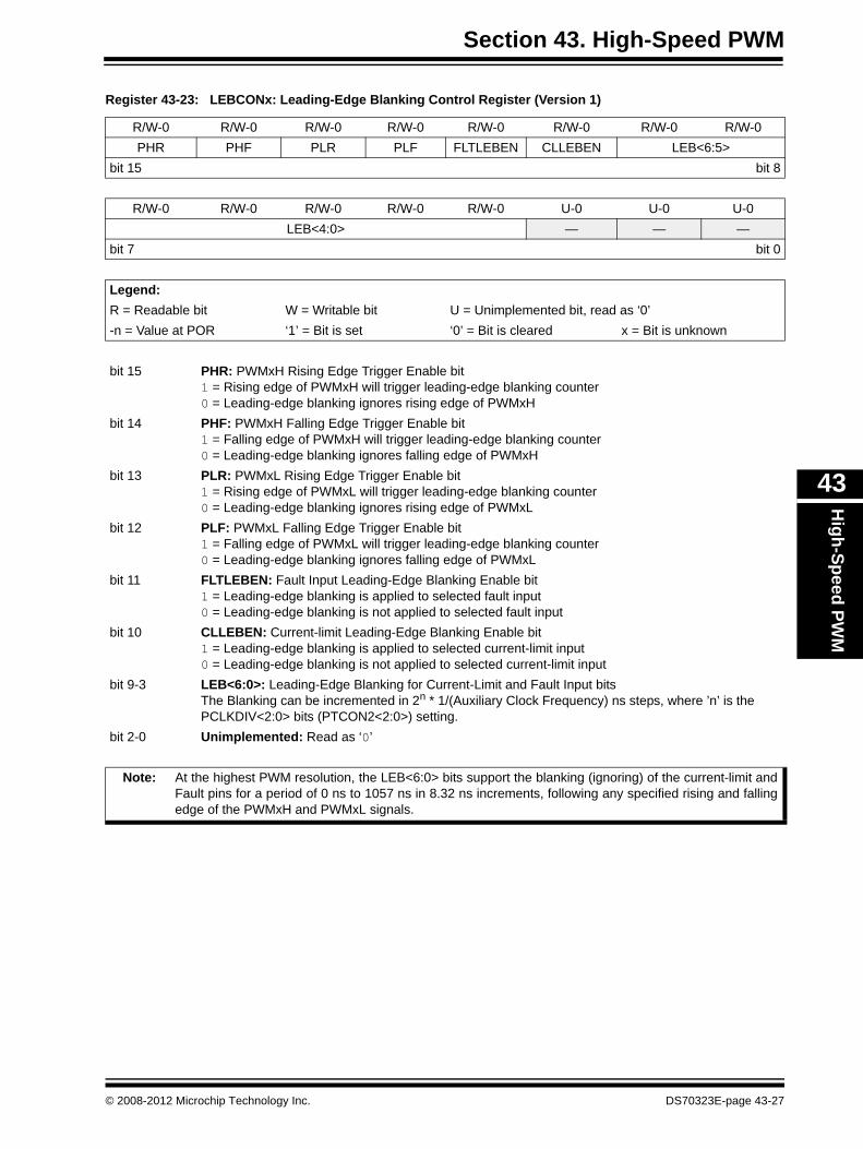
Register 43-23: LEBCONx: Leading-Edge Blanking Control Register (Version 1)
R/W-0 R/W-0 R/W-0 R/W-0 R/W-0 R/W-0 R/W-0 R/W-0PHR PHF PLR PLF FLTLEBEN CLLEBEN LEB<6:5>
bit 15 bit 8
R/W-0 R/W-0 R/W-0 R/W-0 R/W-0 U-0 U-0 U-0LEB<4:0> — — —
bit 7 bit 0
Legend:R = Readable bit W = Writable bit U = Unimplemented bit, read as ‘0’-n = Value at POR ‘1’ = Bit is set ‘0’ = Bit is cleared x = Bit is unknown
bit 15 PHR: PWMxH Rising Edge Trigger Enable bit1 = Rising edge of PWMxH will trigger leading-edge blanking counter0 = Leading-edge blanking ignores rising edge of PWMxH
bit 14 PHF: PWMxH Falling Edge Trigger Enable bit1 = Falling edge of PWMxH will trigger leading-edge blanking counter0 = Leading-edge blanking ignores falling edge of PWMxH
bit 13 PLR: PWMxL Rising Edge Trigger Enable bit1 = Rising edge of PWMxL will trigger leading-edge blanking counter0 = Leading-edge blanking ignores rising edge of PWMxL
bit 12 PLF: PWMxL Falling Edge Trigger Enable bit1 = Falling edge of PWMxL will trigger leading-edge blanking counter0 = Leading-edge blanking ignores falling edge of PWMxL
bit 11 FLTLEBEN: Fault Input Leading-Edge Blanking Enable bit1 = Leading-edge blanking is applied to selected fault input0 = Leading-edge blanking is not applied to selected fault input
bit 10 CLLEBEN: Current-limit Leading-Edge Blanking Enable bit1 = Leading-edge blanking is applied to selected current-limit input0 = Leading-edge blanking is not applied to selected current-limit input
bit 9-3 LEB<6:0>: Leading-Edge Blanking for Current-Limit and Fault Input bitsThe Blanking can be incremented in 2n * 1/(Auxiliary Clock Frequency) ns steps, where ’n’ is the PCLKDIV<2:0> bits (PTCON2<2:0>) setting.
bit 2-0 Unimplemented: Read as ‘0’
Note: At the highest PWM resolution, the LEB<6:0> bits support the blanking (ignoring) of the current-limit andFault pins for a period of 0 ns to 1057 ns in 8.32 ns increments, following any specified rising and fallingedge of the PWMxH and PWMxL signals.
© 2008-2012 Microchip Technology Inc. DS70323E-page 43-27

dsPIC33F/PIC24H Family Reference Manual
Register 43-24: LEBCONx: Leading-Edge Blanking Control Register (Version 2)
R/W-0 R/W-0 R/W-0 R/W-0 R/W-0 R/W-0 U-0 U-0PHR PHF PLR PLF FLTLEBEN CLLEBEN — —
bit 15 bit 8
U-0 U-0 R/W-0 R/W-0 R/W-0 R/W-0 R/W-0 R/W-0— — BCH(1) BCL BPHH BPHL BPLH BPLL
bit 7 bit 0
Legend:R = Readable bit W = Writable bit U = Unimplemented bit, read as ‘0’-n = Value at POR ‘1’ = Bit is set ‘0’ = Bit is cleared x = Bit is unknown
bit 15 PHR: PWMxH Rising Edge Trigger Enable bit1 = Rising edge of PWMxH will trigger Leading-Edge Blanking counter0 = Leading-Edge Blanking ignores rising edge of PWMxH
bit 14 PHF: PWMxH Falling Edge Trigger Enable bit1 = Falling edge of PWMxH will trigger Leading-Edge Blanking counter0 = Leading-Edge Blanking ignores falling edge of PWMxH
bit 13 PLR: PWMxL Rising Edge Trigger Enable bit1 = Rising edge of PWMxL will trigger Leading-Edge Blanking counter0 = Leading-Edge Blanking ignores rising edge of PWMxL
bit 12 PLF: PWMxL Falling Edge Trigger Enable bit1 = Falling edge of PWMxL will trigger Leading-Edge Blanking counter0 = Leading-Edge Blanking ignores falling edge of PWMxL
bit 11 FLTLEBEN: Fault Input Leading-Edge Blanking Enable bit1 = Leading-Edge Blanking is applied to selected Fault input0 = Leading-Edge Blanking is not applied to selected Fault input
bit 10 CLLEBEN: Current-Limit Leading-Edge Blanking Enable bit1 = Leading-Edge Blanking is applied to selected current-limit input0 = Leading-Edge Blanking is not applied to selected current-limit input
bit 9-6 Unimplemented: Read as ‘0’bit 5 BCH: Blanking in Selected Blanking Signal High Enable bit(1)
1 = State blanking (of current-limit and/or Fault input signals) when selected blanking signal is high0 = No blanking when selected blanking signal is high
bit 4 BCL: Blanking in Selected Blanking Signal Low Enable bit(1)
1 = State blanking (of current-limit and/or Fault input signals) when selected blanking signal is low0 = No blanking when selected blanking signal is low
bit 3 BPHH: Blanking in PWMxH High Enable bit1 = State blanking (of current-limit and/or Fault input signals) when PWMxH output is high0 = No blanking when PWMxH output is high
bit 2 BPHL: Blanking in PWMxH Low Enable bit1 = State blanking (of current-limit and/or Fault input signals) when PWMxH output is low0 = No blanking when PWMxH output is low
bit 1 BPLH: Blanking in PWMxL High Enable bit1 = State blanking (of current-limit and/or Fault input signals) when PWMxL output is high0 = No blanking when PWMxL output is high
bit 0 BPLL: Blanking in PWMxL Low Enable bit1 = State blanking (of current-limit and/or Fault input signals) when PWMxL output is low0 = No blanking when PWMxL output is low
Note 1: The blanking signal is selected through the BLANKSEL bits in the AUXCONx register.
DS70323E-page 43-28 © 2008-2012 Microchip Technology Inc.

Section 43. High-Speed PWMH
igh-Speed PWM
43
Register 43-25: LEBDLYx: Leading-Edge Blanking Delay Register
U-0 U-0 U-0 U-0 R/W-0 R/W-0 R/W-0 R/W-0— — — — LEB<8:5>
bit 15 bit 8
R/W-0 R/W-0 R/W-0 R/W-0 R/W-0 U-0 U-0 U-0LEB<4:0> — — —
bit 7 bit 0
Legend:R = Readable bit W = Writable bit U = Unimplemented bit, read as ‘0’-n = Value at POR ‘1’ = Bit is set ‘0’ = Bit is cleared x = Bit is unknown
bit 15-12 Unimplemented: Read as ‘0’bit 11-3 LEB<8:0>: Leading-Edge Blanking Delay bits for Current-Limit and Fault Inputs
Value in 8.32 ns increments.bit 2-0 Unimplemented: Read as ‘0’
Note: At the highest PWM resolution, the LEB<8:0> bits support the blanking (ignoring) of the current-limit andFault pins for a period of 0 ns to 4252 ns in 8.32 ns increments, following any specified rising and fallingedge of the PWMxH and PWMxL signals.
© 2008-2012 Microchip Technology Inc. DS70323E-page 43-29
dsPIC33F/PIC24H Family Reference Manual
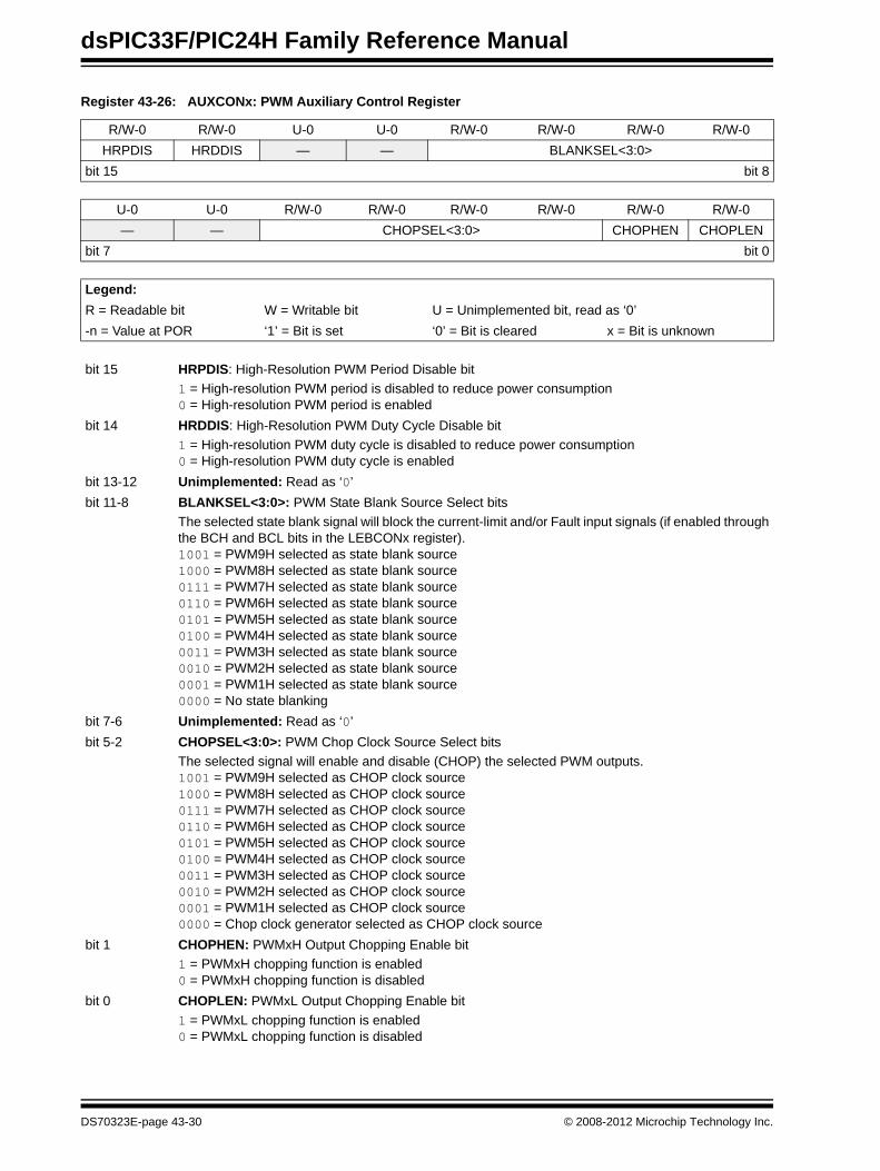
Register 43-26: AUXCONx: PWM Auxiliary Control Register
R/W-0 R/W-0 U-0 U-0 R/W-0 R/W-0 R/W-0 R/W-0HRPDIS HRDDIS — — BLANKSEL<3:0>
bit 15 bit 8
U-0 U-0 R/W-0 R/W-0 R/W-0 R/W-0 R/W-0 R/W-0— — CHOPSEL<3:0> CHOPHEN CHOPLEN
bit 7 bit 0
Legend:R = Readable bit W = Writable bit U = Unimplemented bit, read as ‘0’-n = Value at POR ‘1’ = Bit is set ‘0’ = Bit is cleared x = Bit is unknown
bit 15 HRPDIS: High-Resolution PWM Period Disable bit1 = High-resolution PWM period is disabled to reduce power consumption0 = High-resolution PWM period is enabled
bit 14 HRDDIS: High-Resolution PWM Duty Cycle Disable bit1 = High-resolution PWM duty cycle is disabled to reduce power consumption0 = High-resolution PWM duty cycle is enabled
bit 13-12 Unimplemented: Read as ‘0’bit 11-8 BLANKSEL<3:0>: PWM State Blank Source Select bits
The selected state blank signal will block the current-limit and/or Fault input signals (if enabled throughthe BCH and BCL bits in the LEBCONx register).1001 = PWM9H selected as state blank source1000 = PWM8H selected as state blank source0111 = PWM7H selected as state blank source0110 = PWM6H selected as state blank source0101 = PWM5H selected as state blank source0100 = PWM4H selected as state blank source0011 = PWM3H selected as state blank source0010 = PWM2H selected as state blank source0001 = PWM1H selected as state blank source0000 = No state blanking
bit 7-6 Unimplemented: Read as ‘0’bit 5-2 CHOPSEL<3:0>: PWM Chop Clock Source Select bits
The selected signal will enable and disable (CHOP) the selected PWM outputs.1001 = PWM9H selected as CHOP clock source1000 = PWM8H selected as CHOP clock source0111 = PWM7H selected as CHOP clock source0110 = PWM6H selected as CHOP clock source0101 = PWM5H selected as CHOP clock source0100 = PWM4H selected as CHOP clock source0011 = PWM3H selected as CHOP clock source0010 = PWM2H selected as CHOP clock source0001 = PWM1H selected as CHOP clock source0000 = Chop clock generator selected as CHOP clock source
bit 1 CHOPHEN: PWMxH Output Chopping Enable bit1 = PWMxH chopping function is enabled0 = PWMxH chopping function is disabled
bit 0 CHOPLEN: PWMxL Output Chopping Enable bit1 = PWMxL chopping function is enabled0 = PWMxL chopping function is disabled
DS70323E-page 43-30 © 2008-2012 Microchip Technology Inc.

Section 43. High-Speed PWMH
igh-Speed PWM
43
Register 43-27: PWMCAPx: Primary PWM Time Base Capture Register
R-0 R-0 R-0 R-0 R-0 R-0 R-0 R-0PWMCAP<12:5>
bit 15 bit 8
R-0 R-0 R-0 R-0 R-0 U-0 U-0 U-0PWMCAP<4:0> — — —
bit 7 bit 0
Legend:R = Readable bit W = Writable bit U = Unimplemented bit, read as ‘0’-n = Value at POR ‘1’ = Bit is set ‘0’ = Bit is cleared x = Bit is unknown
bit 15-3 PWMCAP<12:0>: Captured PWM Time Base Value bitsThe value in this register represents the captured PWM time base value when a leading edge isdetected on the current-limit input.
bit 2-0 Unimplemented: Read as ‘0’
Note 1: The Capture feature is available only on primary output (PWMxH).
2: This feature is active only after the LEB processing on the current-limit input signal is complete.
3: The minimum capture resolution is 8.32 ns.
4: This feature can be used only when XPRES = 0 (PWMCONx<1>).
© 2008-2012 Microchip Technology Inc. DS70323E-page 43-31

dsPIC33F/PIC24H Family Reference Manual
43.4 ARCHITECTURE OVERVIEWFigure 43-1 illustrates an architectural overview of the High-Speed PWM module and itsinterconnection with the CPU and other peripherals.
Figure 43-1: High-Speed PWM Module Architectural Overview
CPU
Master Time Base
PWMGenerator 1
PWMGenerator 2
PWMGenerator 8
PWMGenerator 9
SYNCI1/2/3/4
SYNCO
PWM1H
PWM1L
PWM1 Interrupt
PWM2H
PWM2L
PWM2 Interrupt
PWM8H
PWM8L
PWM8 Interrupt
PWM9H
PWM9L
PWM9 Interrupt
Synchronization Signal
Data Bus
ADC ModuleFault and
Fault, Current-Limit
Synchronization Signal
Synchronization Signal
Synchronization Signal
Primary Trigger
Secondary Trigger
Special Event Trigger
Current Limit
and Dead-Time Compensation
Fault, Current-Limitand Dead-Time Compensation
Fault, Current-Limitand Dead-Time Compensation
PWM3 through PWM7
Secondary SpecialEvent Trigger
Primary SpecialEvent Trigger Interrupt
Secondary SpecialEvent Trigger Interrupt
DS70323E-page 43-32 © 2008-2012 Microchip Technology Inc.

Section 43. High-Speed PWMH
igh-Speed PWM
43
The High-Speed PWM module contains upto nine PWM generators. Each PWM generatorprovides two PWM outputs: PWMxH and PWMxL. A master time base generator provides asynchronous signal as a common time base to synchronize the various PWM outputs. Eachgenerator can operate independently or in synchronization with the master time base. Theindividual PWM outputs are available on the output pins of the device. The input fault signals andcurrent-limit signals, when enabled, can monitor and protect the system by placing the PWMoutputs into a known “safe” state.
Each PWM can generate a trigger to the ADC module to sample the analog signal at a specificinstance during the PWM period. In addition, the High-Speed PWM module also generates aSpecial Event Trigger to the ADC module based on the master time base.
In Master Time Base mode, the High-Speed PWM module can synchronize itself with an externalsignal or can act as a synchronizing source to any external device. The SYNCIx pins are the inputpins, which can synchronize the High-Speed PWM module with an external signal. The SYNCOpin is an output pin that provides a synchronous signal to an external device.
The High-Speed PWM module can be used for a wide variety of power conversion applicationsthat require the following:
• High operating frequencies with good resolution• Ability to dynamically control PWM parameters, such as duty cycle, period and dead time• Ability to independently control each PWM• Ability to synchronously control all PWMs• Independent resource allocation for each PWM generator• Fault handling capability• CPU load staggering to execute multiple control loops
Each High-Speed PWM module function is described in the subsequent sections. Figure 43-2illustrates the interconnection between various registers in the High-Speed PWM module.
© 2008-2012 Microchip Technology Inc. DS70323E-page 43-33

dsPIC33F/PIC24H Family Reference Manual
Figure 43-2: High-Speed PWM Module Register Interconnection Diagram
MUX
PTMRx
PDCx
PWMCONx TRGCONx
PTCON, PTCON2
IOCONx
DTRx
PWMxL
PWMxH
FLTx or
PWM1L
PWM1H
FCLCONx
MDC
PHASEx
LEBCONx
MUX
STMRx
SDCx
SPHASEx ALTDTRx
PWMCAPx
User Override Logic
Current-Limit
PWM Output Mode Control Logic
Logic
Pin Control Logic
Fault and Current-Limit
Logic
PWM Generator 1
FLTx orPWM Generator 2 through PWM Generator 9
InterruptLogic
ADC Trigger
Module Control and Timing
Master Duty Cycle Register
Syn
chro
niza
tion
Syn
chro
niza
tion
Mas
ter P
erio
dM
aste
r Per
iod
Mas
ter D
uty
Cyc
leM
aste
r Dut
y C
ycle
Secondary PWM
SYNCI2SYNCI1
SYNCO1SEVTCMP
Comparator Special Event TriggerSpecial Event
Postscaler
PTPER
PMTMR Primary Master Time Base
Primary Master Time Base Counter
Special Event Compare Trigger
Comparator
Clock Prescaler
Comparator
Comparator
Comparator
16-B
it D
ata
Bus Dead-Time
TRIGx Fault Override Logic
Override Logic
SYNCO2SSEVTCMP
Comparator SecondarySecondary SpecialEvent Postscaler
STPER
SMTMR Secondary Master Time Base
Secondary Master Time Base Counter
Secondary Special Event
Comparator
Clock Prescaler
DTCMPx
SYNCI4SYNCI3
SYNCI2SYNCI1 SYNCI4SYNCI3
Special Event
Compare Trigger
Trigger
AnalogComparator
AnalogComparator
DTCMPx
DS70323E-page 43-34 © 2008-2012 Microchip Technology Inc.

Section 43. High-Speed PWMH
igh-Speed PWM
43
43.5 MODULE DESCRIPTION
43.5.1 PWM Clock SelectionThe auxiliary clock generator must be used to generate the clock for the PWM moduleindependent of the system clock. The Primary Oscillator Clock (POSCCLK), PrimaryPhase-Locked Loop (PLL) Output (FVCO), and Internal FRC Clock (FRCCLK) can be used withan auxiliary PLL to obtain the Auxiliary Clock (ACLK). The auxiliary PLL consists of a fixed 16xmultiplication factor. Example 43-1 shows the configuration of auxiliary clock using FRC.Example 43-2 shows the configuration of auxiliary clock using primary oscillator (POSC).
The Auxiliary Clock Control register (ACLKCON) selects the reference clock and enables theauxiliary PLL and output dividers for obtaining the necessary auxiliary clock. Equation 43-1provides the relationship between the Reference Clock (REFCLK) input frequency and the ACLKfrequency. Figure 43-3 illustrates the oscillator system.
Figure 43-3: Oscillator System
÷ N
ACLK
SELACLK APSTSCLR<2:0>
To PWM/ADC
ENAPLL
APLLx16
ASRCSEL FRCSEL
POSCCLKFRCCLK
÷ N
ROSEL RODIV<3:0>
REFCLKO(3)
POSCCLK
Reference Clock Generation
Auxiliary Clock Generation
Note 1: Refer to the “Oscillator Configuration” chapter in the specific device data sheet for PLL details.2: If the Oscillator is used with XT or HS modes, an external parallel resistor with the value of 1 MΩ must be connected.3: REFCLK0 functionality is not available if the Primary Oscillator is used.
FVCO(1)
FOSC
Secondary Oscillator
LPOSCEN
SOSCO
SOSCI
Timer 1
OSC2
OSC1Primary Oscillator
XTPLL, HSPLL,
XT, HS, EC
FRCDIV<2:0>
WDT, PWRT, FSCM
FRCDIVN
SOSC
FRCDIV16
ECPLL, FRCPLL
NOSC<2:0> FNOSC<2:0>
Reset
FRCOscillator
LPRCOscillator
DOZE<2:0>
S3
S1
S2
S1/S3
S7
S6
FRC
LPRC
S0
S5
S4
÷ 16
Clock Switch
S7
Clock Fail
÷ 2
TUNE bits
PLL(1) FCY
FOSC
FRC
DIV
DO
ZE
FVCO(1)
To ADC andAuxiliary ClockGenerator
R(2)
POSCMD<1:0>
POSCCLK
FP
(112 MHz - 120 MHz max)
© 2008-2012 Microchip Technology Inc. DS70323E-page 43-35

dsPIC33F/PIC24H Family Reference Manual
For devices with remappable I/O, refer to Section 42. “Oscillator (Part IV)” (DS70307), formore information on configuring the clock generator. For devices without remappable I/O, referto Section 48. “Oscillator (Part V)” (DS70596).Equation 43-1: ACLK Frequency Calculation
Example 43-1: Using FRC for Setting the ACLK
Example 43-2: Using POSC for Setting the ACLK
ACLK REFCLK M1×N
--------------------------------------=
Where,
REFCLK = Internal FRC Clock frequency (7.37 MHz), if the Internal FRC is selected as theclock source
(or)
REFCLK = Primary Oscillator Clock frequency (POSCCLK), if the Primary Oscillator (POSC)is selected as the clock source
M1 = 16, if the auxiliary PLL is enabled by setting the ENAPLL bit (ACLKCON<15>)
(or)
M1 = 1, if the auxiliary PLL is disabled
N = Postscaler ratio selected by the Auxiliary Postscaler bits (APSTSCLR<2:0>) in theAuxiliary Clock Control register (ACLKCON<2:0>)
Note 1: The nominal input clock to the PWM should be 120 MHz. Refer to the “ElectricalCharacteristics” chapter in the specific device data sheet for the full operatingrange.
2: Use the TUN<5:0> bits of OSCTUN register to tune the FRC clock frequency to7.49 MHz to obtain a maximum PWM resolution of 1.04 ns. Refer to the “OscillatorConfiguration” section of the device data sheet for more information.
3: The auxiliary clock post scaler must be configured toDivide-by-1 (APSTSCLR<2:0>) = 111), for proper operation of the PWM module.
/* Setup for the Auxiliary clock to use the FRC as the REFCLK *//* ((FRC * 16) / APSTSCLR) = (7.49 * 16) / 1 = 119.84 MHz */ACLKCONbits.FRCSEL = 1; /* FRC is input to Auxiliary PLL */ACLKCONbits.SELACLK = 1; /* Auxiliary Oscillator provides the clock
source */ACLKCONbits.APSTSCLR = 7; /* Divide Auxiliary clock by 1 */ACLKCONbits.ENAPLL = 1; /* Enable Auxiliary PLL */while(ACLKCONbits.APLLCK != 1); /* Wait for Auxiliary PLL to Lock */
/* Setup for the Auxiliary clock to use the primary oscillator(7.37 MHz) as the REFCLK */
/*((primary oscillator* 16) / APSTSCLR) = (7.37 * 16) / 1 = 117.9 MHz */
/* Primary Oscillator is the Clock Source */ACLKCONbits.ARCSEL = 1;
/* Input clock source is determined by ASRCSEL bit setting */ACLKCONbits.FRCSEL = 0;
/* Auxiliary Oscillator provides the clock source */ACLKCONbits.SELACLK = 1;
/* Divide Auxiliary clock by 1 */ACLKCONbits.APSTSCLR = 7;
/* Enable Auxiliary PLL */ACLKCONbits.ENAPLL = 1;
/* Wait for Auxiliary PLL to Lock */while(ACLKCONbits.APLLCK != 1);
DS70323E-page 43-36 © 2008-2012 Microchip Technology Inc.

Section 43. High-Speed PWMH
igh-Speed PWM
43
The ACLK for the PWM module can be derived from the system clock while the device is runningin the primary PLL mode. Equation 43-3 provides the relationship between the FVCO frequencyand ACLK frequency. The block diagram for FVCO as the clock source for ACLK is illustrated inFigure 43-4. The formula to calculate Fvco is shown in Equation 43-2. The example for usingFVCO as the auxiliary clock source is shown in Example 43-3.
Figure 43-4: FVCO is the Clock Source for Auxiliary Clock
Equation 43-2: FVCO Calculation
Equation 43-3: ACLK Frequency Calculation using FVCO
0.8 MHz - 8.0 MHzHere(1) 112 MHz -120 MHz
Here(1)
Divide by2, 4, 8
Divide by2-513
Divide by2-33
Source (Crystal, ExternalPLLPRE X VCO
PLLDIV
PLLPOSTClock or Internal RC)
12.5 MHz - 60 MHzHere(1)
FOSC
FVCO
N1
M
N2
Note 1: This frequency range must be satisfied when using FVCO as the clock source for Auxiliary Clock.
FIN
FVCOFIN M×
N1-------------------- FIN
PLLDIV 2+PLLPRE 2+--------------------------------⎝ ⎠⎛ ⎞×= =
Where,
FVCO = VCO output frequency
FIN = Input frequency from source (Crystal, External Clock, or Internal RC)
M = PLL feedback divider selected by PLLDIV<8:0>
N1 = PLL prescaler ratio selected by PLLPRE<4:0>
ACLKFVCO
N-------------=
Where,
N = Postscaler ratio selected by the APSTSCLR<2:0> bits (ACLKCON<2:0>)
FVCO = VCO output frequency
ACLK = Auxiliary clock frequency
Note: If the primary PLL is used as a source for the auxiliary clock, then the primary PLLshould be configured up to a maximum operation of FCY = 30 MHz or less, and FVCOmust be in the range of 112 MHz to 120 MHz. The minimum PWM resolution whenFvco is the clock source for the auxiliary clock is 8.32 ns.
© 2008-2012 Microchip Technology Inc. DS70323E-page 43-37

dsPIC33F/PIC24H Family Reference Manual
Example 43-3: Using FVCO as the Auxiliary Clock Source
43.5.2 Time BaseEach PWM output in a PWM generator can use either the master time base or an independenttime base. The High-Speed PWM module input clock consists of the prescaler (divider)options 1:1 to 1:64, which can be selected using the PWM Input Clock Prescaler (Divider) Selectbits (PCLKDIV<2:0>) in the PWM Generator Duty Cycle register (PTCON2<2:0>). This prescaleraffects all PWM time bases. The prescaled value will also reflect the PWM resolution, whichhelps to reduce the power consumption of the High-Speed PWM module. The prescaled clock isthe input to the PWM clock control logic block. The maximum clock rate provides a duty cycleand period resolution of 1.04 ns. For example:• If a prescaler option 1:2 is selected with ACLK = 120 MHz, the PWM duty cycle and period
resolution can be set at 2.08 ns. Therefore, the power consumption of the High-Speed PWM module is reduced by approximately 50 percent of the maximum speed operation.
• If a prescaler option 1:4 is selected with ACLK = 120 MHz, the PWM duty cycle and period resolution can be set at 4.16 ns. Therefore, the power consumption of the High-Speed PWM module is reduced by approximately 75 percent of the maximum speed operation.
The High-Speed PWM module can operate in either the standard edge-aligned or center-alignedtime base.
43.5.3 Standard Edge-Aligned PWMFigure 43-5 illustrates the standard edge-aligned PWM waveforms. To create the edge-alignedPWM, a timer or counter circuit counts upward from zero to a specified maximum value, calledthe Period. Another register contains the duty cycle value, which is constantly compared with thetimer (period) value. When the timer or counter value is less than or equal to the duty cycle value,the PWM output signal is asserted. When the timer value exceeds the duty cycle value, the PWMsignal is deasserted. When the timer is greater than or equal to the period value, the timer resetsitself, and the process repeats.
Figure 43-5: Standard Edge-Aligned PWM Mode
/* Assume Primary Oscillator is 8 MHz and FCY = 30 MHz. *//* Therefore, FOSC = 60 MHz *//* Setup for the Auxiliary clock to use Fvco as the source *//* Fosc = Primary Oscillator * (PLLDIV / PLLPOST * PLLPRE) *//* Fvco = Fosc * N2 *//* Fosc = 60 MHz; N2 = 2; Fvco = 120 MHz; M = 30 *//* Input to the Vco = 4 MHz; N1 = 2; Fin = 8 MHz */
ACLKCONbits.SELACLK = 0; /* Primary PLL (Fvco) provides the source clock for the auxiliary clock divider */
/* Configuring PLL prescaler, PLL Post scaler, PLL divider */PLLFBD = 28; /* M = 30 */CLKDIVbits.PLLPOST = 0; /* N1 = 2 */CLKDIVbits.PLLPRE = 0; /* N2 = 2 */ACLKCONbits.APSTSCLR = 7; /* Divide Auxiliary click by 1 */while (OSCCONbits.LOCK == 1);/* Wait for PLL to lock */
Period
PWM1H
TON TOFF
Period
Duty Cycle
0
Period
TimerValue
Timer Resets
PWMxH
Value
Duty Cycle Match
New Duty Cycle
DS70323E-page 43-38 © 2008-2012 Microchip Technology Inc.

Section 43. High-Speed PWMH
igh-Speed PWM
43
43.5.4 Center-Aligned PWMThe center-aligned PWM waveforms as illustrated in Figure 43-6, align the PWM signals to areference point such that half of the PWM signal occurs before the reference point and theremaining half of the signal occurs after the reference point. Center-aligned mode is enabledwhen the Center-Aligned Mode Enable bit (CAM) in the PWM Control register (PWMCONx<2>)is set.When operating in Center-aligned mode, the effective PWM period is twice the value that isspecified in the PWM Primary Phase Shift registers (PHASEx) because the independent timebase counter in the PWM generator is counting up and then counting down during the cycle. Theup/down count sequence doubles the effective PWM cycle period. This mode is used in manymotor control and uninterrupted power supply applications. The configuration of edge-aligned orcenter-aligned mode selection is shown in Example 43-4. The typical application ofcenter-aligned PWM mode in UPS applications is illustrated in Figure 43-7.
Figure 43-6: Center-Aligned PWM Mode
Example 43-4: Edge-Aligned or Center-Aligned Mode Selection
Figure 43-7: Center-Aligned PWM Mode in Power Inverter/UPS Applications
Note: Independent Time Base mode (ITB = 1) must be enabled to use Center-alignedmode. If ITB = 0, the CAM bit (PWMCONx<2>) is ignored.
PHASEX
Local Time-Base Value
2 x Period
Period
0
PDC1
PDC2
PWM1H
PWM2H
/* Select Edge-Aligned PWM */
PWMCON1bits.CAM = 0; /* For Edge-Aligned Mode */
/* Select Center-Aligned PWM */
PWMCON1bits.CAM = 1; /* For Center-Aligned Mode */PWMCON1bits.ITB = 1; /* Enable Independent Time Base */
VDC
S3
N
L
S1
S2 S4
+
–
PWM1H PWM2H
PWM2LPWM1L
IL
© 2008-2012 Microchip Technology Inc. DS70323E-page 43-39

dsPIC33F/PIC24H Family Reference Manual
43.5.4.1 ADVANTAGES OF CENTER-ALIGNED MODE IN UPS APPLICATIONS
The current ripple frequency and noise frequency are double the switch frequency. A lowermagnitude of current ripple is achieved as the switch frequency of the current ripple is doubled.Lower current ripple contributes to relaxed requirements for the DC input capacitor and outputfilter inductor and capacitor. Lower current ripple contributes to lower output current harmonics.Figure 43-8 illustrates the typical waveforms of UPS, configured for Unipolar Gate Drive inCenter-aligned mode.
Figure 43-8: Unipolar Gate Drive in Center-Aligned Mode
PWM1H
PWM1L
PWM2H
PWM2L
IL
PTPER
PDC2PDC1
DS70323E-page 43-40 © 2008-2012 Microchip Technology Inc.

Section 43. High-Speed PWMH
igh-Speed PWM
43
43.5.5 Master Time Base/Synchronous Time BaseThe PWM functionality in the master time base is illustrated in Figure 43-9.
Figure 43-9: Master Time Base Block Diagram
Some of the common tasks of the master time base are:
• Generates time reference for all the PWM generators• Generates special event ADC trigger and interrupt• Supports synchronization with the external SYNC signal
(SYNCI1/SYNCI2/SYNCI3/SYNCI4)• Supports synchronization with external devices using the SYNCO signal
The master time base for a PWM generator is set by loading a 16-bit value into the Time Periodregister (PTPER/STPER). In the Master Time Base mode, the value in the PHASEx andSPHASEx registers provide phase shift between the PWM outputs. The clock for the PWMtimer (PMTMR/SMTMR) is derived from the system clock.
MUX
SYNCSRC
PMTMR/
SEVTCMP/
1:1
1:16
PTPER/
SEVTPS
Reset
SYNCENSYNCI1
SYNCI2
SYNCOEN
SYNCO
Edge Detector
SYNCPOL
Special EventTrigger to ADC
Synchronization Signal
PWM Clock
STPER
SMTMR
SSEVTCMP
SYNCI3
SYNCI4
© 2008-2012 Microchip Technology Inc. DS70323E-page 43-41

dsPIC33F/PIC24H Family Reference Manual
43.5.6 Time Base SynchronizationThe master time base can be synchronized with the external synchronization signal through themaster time base synchronization signal (SYNCI1/SYNCI2/SYNCI3/SYNCI4). Thesynchronization source (SYNCI1, SYNCI2, SYNCI3 and SYNCI4), can be selected using theSynchronous Source Selection bits (SYNCSRC<1:0>) in the PWM Time Base Control register(PTCON<5:4>). The Synchronize Input Polarity bit (SYNCPOL) in the PWM Time Base Controlregister (PTCON<9>/STCON<9>), selects the rising or falling edge of the synchronization pulse,which resets the timer (PMTMR/SMTMR). The External Synchronization feature can be enabledor disabled with the External Time Base Synchronization Enable bit (SYNCEN) in the PWM TimeBase Control register (PTCON<7>/STCON<7>). The pulse width of the external synchronizationsignal (SYNCI1/SYNCI2/SYNCI3/SYNCI4) should be more than 200 ns to ensure the reliabledetection by the master time base.
The external device can also be synchronized with the master time base using thesynchronization output signal (SYNCO). The SYNCO signal is generated when thePTPER/STPER register resets the PMTMR/SMTMR timer. The SYNCO signal pulse is 12 TCYclocks wide (about 300 ns at 40 MIPS) to ensure other devices can sense the signal. The polarityof the SYNCO signal is determined by the SYNCPOL bit in the PTCON/STCON register. TheSYNCO signal can be enabled or disabled by selecting the Primary Time Base Sync Enable bit(SYNCOEN) in the PTCON/STCON register (PTCON<8>/STCON<8>).
The advantage of synchronization is that it ensures the beat frequencies are not generated whenmultiple power controllers are in use. The configuration of synchronizing master time base withexternal signal is shown in Example 43-5.
Example 43-5: Synchronizing Master Time Base with External Signal
The configuration of synchronizing external device with master time base is shown inExample 43-6.
Example 43-6: Synchronizing External Device with Master Time Base
Note 1: The period of SYNCI pulse should be larger than the PWM period value.
2: The SYNCI pulse should be continuous with a minimum pulse width of 200 ns.
3: The PWM cycles are expected to be distorted for the first two SYNCI pulses.
4: The period value should be a multiple of 8 (Least Significant 3 bits set to ‘0’) for theexternal synchronization to work in the Push-Pull mode.
5: When using external synchronization in the push-pull mode, the externalsynchronization signal must be generated at twice the frequency of the desiredPWM frequency.
6: There is a delay from the input of a SYNC signal until the internal time base counteris Reset. This will be approximately 30 ns.
7: The External Time Base Synchronization must not be used with phase shiftedPWM as the synchronization signal may not maintain the phase relationshipsbetween the multiple PWM channels.
8: The External Time Base Synchronization cannot be used in Independent TimeBase mode.
/* Synchronizing Master Time base with External Signal */
PTCONbits.SYNCSRC = 0; /* Select SYNC1 input as synchronizing source */PTCONbits.SYNCPOL = 0; /* Rising edge of SYNC1 resets the PWM Timer */PTCONbits.SYNCEN = 1; /* Enable external synchronization */
/* Synchronizing external device with Master time base */
PTCONbits.SYNCPOL = 0; /* SYNCO output is active-high */PTCONbits.SYNCOEN = 1; /* Enable SYNCO output */
DS70323E-page 43-42 © 2008-2012 Microchip Technology Inc.

Section 43. High-Speed PWMH
igh-Speed PWM
43
43.5.7 Special Event TriggerThe High-Speed PWM module consists of a master Special Event Trigger that can be used as aCPU interrupt source and for synchronization of analog-to-digital conversions with the PWM timebase. The analog-to-digital sampling time can be programmed to occur any time within the PWMperiod. The Special Event Trigger allows the user-assigned application to minimize the delaybetween the time the analog-to-digital conversion results are acquired and the time the duty cyclevalue is updated. The Special Event Trigger is based on the master time base.
The master Special Event Trigger value is loaded into the PWM Special Event Compareregister (SEVTCMP/SSEVTCMP). In addition, the PWM Special Event Trigger OutputPostscaler Select bits (SEVTPS<3:0>) in the PWM Time Base Control register (PTCON<3:0>)or the PWM Secondary Master Time Base Control register (STCON<3:0>), control the SpecialEvent Trigger operation. To generate a trigger to the ADC module, the value in the PWM MasterTime Base Counter (PMTMR/SMTMR) is compared to the value in the SEVTCMP/SSEVTCMPregister. The Special Event Trigger consists of a postscaler that allows 1:1 to 1:16 postscalerratio. The postscaler is configured by writing to the (SEVTPS<3:0>) control bits (PTCON<3:0>).
Special Event Trigger pulses are generated if the following conditions are satisfied:
• On a match condition regardless of the status of the Special Event Interrupt Enable bit, SEIEN bit (PTCON<11>)
• If the compare value in the SEVTCMP/SSEVTCMP register is a value from zero to a maximum value of the PTPER/STPER register
The Special Event Trigger output postscaler is cleared on these events:
• Any device Reset• When PTEN = 0 (PTCON<15>)
The configuration of ADC special event trigger is shown in Example 43-7.
Example 43-7: ADC Special Event Trigger Configuration
In addition to generating ADC triggers, the Special Event Trigger can also be used to generatethe primary and secondary Special Event trigger interrupts, on a compare match event.
/* ADC Special Event Trigger configuration */
SEVTCMP = 1248; /* Special Event Trigger value set at ~25% of period value (4999)*/
PTCONbits.SEVTPS = 0; /* Special Event Trigger output postscaler set to 1:1 selection (trigger generated
every PWM cycle */PTCONbits.SEIEN = 0; /* Special event interrupt is disabled */while (PTCONbits.SESTAT == 0); /* Wait for special event status change */
© 2008-2012 Microchip Technology Inc. DS70323E-page 43-43

dsPIC33F/PIC24H Family Reference Manual
43.5.8 Independent PWM Time BaseThe PWM functionality in the independent time base is illustrated in Figure 43-10.
Figure 43-10: Independent Time Base Block Diagrams for Devices without a Secondary Master Time Base
Figure 43-11: Independent Time Base Block Diagrams for Devices with a Secondary Master Time Base
In Independent Time Base mode, each PWM generator can operate in:
• A shared time base for both the primary (PWMxH) and secondary (PWMxL) outputs
This operation occurs during Complementary, Redundant or Push-Pull mode. Theindependent time base periods for both PWM outputs (PWMxH and PWMxL) are providedby the value in the PHASEx register.
• A dedicated time base for each of the primary (PWMxH) and secondary (PWMxL) outputs
This operation occurs only during Independent Output mode. The independent time baseperiod for PWMxH output is provided by the value in the PHASEx register. The independenttime base period for PWMxL output is provided by the value in the PWM Secondary PhaseShift register (SPHASEx).
PTMRx
PTPER
Equality Comparator
CLK
>
Reset
16
16
MUX
PHASEx
ITB0 1
15 0 15 0
15 0
STMRx
PTPER
Equality Comparator
CLK
>
Reset
16
16
MUX
SPHASEx
ITB0 1
15 0 15 0
15 0
ITB = 1, Controls PWMxH only ITB = 1, Controls PWMxL onlyITB = 0, Controls PWMxH and PWMxL ITB = 0, Not applicable
PTMRx
PTPER/STPER
Equality Comparator
CLK
>
Reset
16
16
MUX
PHASEx
ITBx0 1
15 0 15 0
15 0
STMRx
Equality Comparator
CLK
>
Reset
16
16
MUX
SPHASEx
ITBx0 1
15 0 15 0
15 0
ITB = 1, Controls PWMxH only ITB = 1, Controls PWMxL onlyITB = 0, Controls PWMxH and PWMxL ITB = 0, Not applicable
PTPER/STPER
Note: The PTMRx and STMRx values are not readable to the user-assigned application.
DS70323E-page 43-44 © 2008-2012 Microchip Technology Inc.

Section 43. High-Speed PWMH
igh-Speed PWM
43
43.6 PWM GENERATORThis section describes the functionality of the PWM generator.
43.6.1 PWM PeriodThe PWM period value defines the switching frequency of the PWM pulses. The PWM periodvalue can be controlled either by the PTPER/STPER register, or by the Independent Time PeriodPHASEx and SPHASEx registers for the respective primary and secondary PWM outputs.
The PWM period value can be controlled in two ways when the High-Speed PWM moduleoperates in Independent Time Base mode (PWMCONx<9> = 1):
• In Complementary, Redundant and Push-Pull modes, the PHASEx register controls the PWM period of the PWM output signals (PWMxH and PWMxL).
• In the True Independent PWM Output mode, the PHASEx register controls the PWM period of the PWMxH output signal and the SPHASEx register controls the PWM period of the PWMxL output signal.
For detailed information about various PWM modes and their features, refer to 43.9 “PWMOperating Modes”.
When the High-Speed PWM module operates in the Master Time Base mode, thePTPER/STPER register holds the 16-bit value, that specifies the counting period for thePMTMR/SMTMR timer. When the High-Speed PWM module operates in the Independent TimeBase mode, the PHASEx and SPHASEx registers hold the 16-bit value that specifies thecounting period for the PTMRx and STMRx timer, respectively. The PWM period can be updatedduring run-time by the user-assigned application. The PWM time period can be determined usingEquation 43-4.
Equation 43-4: PERIOD, PHASEx and SPHASEx Register Value Calculation
PTPER STPER PHASEx SPHASEx, , , ACLK 8× DesiredPWMPeriod×PWMInputClockPrescalerDivider PCLKDIV( )----------------------------------------------------------------------------------------------------------------------------⎝ ⎠⎛ ⎞ 8–=
ACLK REFCLK M1×N
--------------------------------------=
ACLKFVCO
N-------------=
Refer to Equation 43-1
Refer to Equation 43-2
(or)
Where,
REFCLK = FRC = 7.49 MHz (ACLKCON<6> = 1)
M1 = 16 Auxiliary PLL (ENAPLL = 1) Enabled
N = Post scaler ratio selected by the Auxiliary Post Scaler bits (APTSTSCLR<2:0>) in theclock control register (ACLKCON<2:0>)
Note 1: Use the TUN<5:0> bits of OSCTUN register to tune the FRC clock frequency to7.49 MHz to obtain a maximum PWM resolution of 1.04 ns. Refer to the “OscillatorConfiguration” section of the device data sheet for more information.
© 2008-2012 Microchip Technology Inc. DS70323E-page 43-45

dsPIC33F/PIC24H Family Reference Manual
Based on Equation 43-4, while operating in the PTPER register or the PHASEx and SPHASExregisters, the register value to be loaded is shown in Example 43-8.
Example 43-8: PWM Time Period Calculation
The maximum available PWM period resolution is 1.04 ns. The PWM Input ClockPrescaler (Divider) Select bits, PCLKDIV<2:0> (PTCON2<2:0>/STCON2<2:0>) determine thetype of PWM clock. The timer/counter is enabled or disabled by setting or clearing the PWMModule Enable bit, PTEN (PTCON<15>). The PMTMR/SMTMR timer is also cleared using thePTEN bit (PTCON<15>).
If the Enable Immediate Period Updates bit, EIPU (PTCON<10>/STCON<10>) is set, the activemaster period register (an internal shadow register) is updated immediately instead of waiting forthe PWM cycle to end. The EIPU bit affects the PMTMR/SMTMR master time base. The clockprescaler selection is shown in Example 43-9. The PWM time period selection is shown inExample 43-10. The PWM time period initialization is shown in Example 43-11.
Example 43-9: Clock Prescaler Selection
Example 43-10: PWM Time Period Selection
Example 43-11: PWM Time Period Initialization
Where,
M1 = 16REFCLK = 7.49 MHz
7.49 MHz1
* 16 ACLK = = 119.84 MHz
N = 1
Desired PWM Period =
1119.84 MHz - 8 = 9579
Desired PWM Switching Frequency
PCLKDIV = 1:11
Desired PWM Switching Frequency = 100 kHz
10 μs* 8 *PTPER, STPER, PHASEx, SPHASEx =
Where,
/* Select PWM time base input clock prescaler *//* Choose divide ratio of 1:2, which affects all PWM timing operations */
PTCON2bits.PCLKDIV = 1;
/* Select time base period control *//* Choose one of these options */
PWMCON1bits.ITB = 0; /* PTPER provides the PWM time period value */
PWMCON1bits.ITB = 1; /* PHASEx/SPHASEx provides the PWM time period value */
/* Choose PWM time period based on FRC input clock *//* PWM frequency is 100 kHz *//* Choose one of the following options */
PTPER = 9579; /* When PWMCONx<9> = 0 */
PHASEx = 9579; /* When PWMCONx<9> = 1 */
SPHASEx = 9579; /* When PWMCONx<9> = 1 */
DS70323E-page 43-46 © 2008-2012 Microchip Technology Inc.

Section 43. High-Speed PWMH
igh-Speed PWM
43
43.6.2 PWM Duty Cycle ControlThe duty cycle determines the period of time that the PWM output must remain in the active state.Each duty cycle register allows a 16-bit duty cycle value that is to be specified. The duty cyclevalues can be updated any time by setting the Immediate Update Enable bit,IUE (PWMCONx<0>). If the IUE bit (PWMCONx<0>) is ‘0’, the active Duty Cycle register (PDCx,SDCx or MDC) updates at the start of the next PWM cycle.
The Master Duty Cycle register (MDC) enables multiple PWM generators to share a commonduty cycle register. The MDC register has an important role in Master Time Base mode.
In addition, each PWM generator has a Primary Duty Cycle register (PDCx) and a SecondaryDuty Cycle register (SDCx) that provides separate duty cycles to each PWM.
43.6.2.1 MASTER DUTY CYCLE (MDC)
The MDC register can be used to provide the same duty cycle to multiple PWM generators. TheMDC register can be used in any PWM mode, and also Master or Independent Time Base. TheMaster Duty Cycle Register Select bit, MDCS (PWMCONx<8>), determines whether the dutycycle of each of the PWMxH and PWMxL outputs are controlled by the PWM MDC register or thePDCx and SDCx registers.
The MDC register enables sharing of the common duty cycle register among multiple PWMgenerators and saves the CPU overhead required in updating multiple duty cycle registers.
43.6.2.2 PRIMARY DUTY CYCLE (PDCx)
The PDCx register can be used for generating the duty cycle for an individual PWM generator.In the Complementary, Redundant or Push-Pull modes, the PDCx register provides the dutycycle for both PWMxH and PWMxL outputs. In Independent Output mode, the PDCx register onlyprovides the duty cycle for the PWMxH output. The primary duty cycle comparison is illustratedin Figure 43-12.
Figure 43-12: Primary Duty Cycle Comparison
43.6.2.3 SECONDARY DUTY CYCLE (SDCx)
The SDCx register is only used in Independent Output mode. It is ignored in Complementary,Redundant and Push-Pull modes. In Independent Output mode, the SDCx register is an inputregister that provides the duty cycle value for the secondary PWM output (PWMxL) signal. Thesecondary duty cycle comparison is illustrated in Figure 43-13.
PDCx Register
PMTMR or PTMRx
Compare Logic PWMxH and/or PWMxL signal
015
15
MUX
MDC Register
MDCS select0 1
CLK
15
0
0
<=
Note: In Independent Output mode, PDCx affects PWMxH only.
© 2008-2012 Microchip Technology Inc. DS70323E-page 43-47
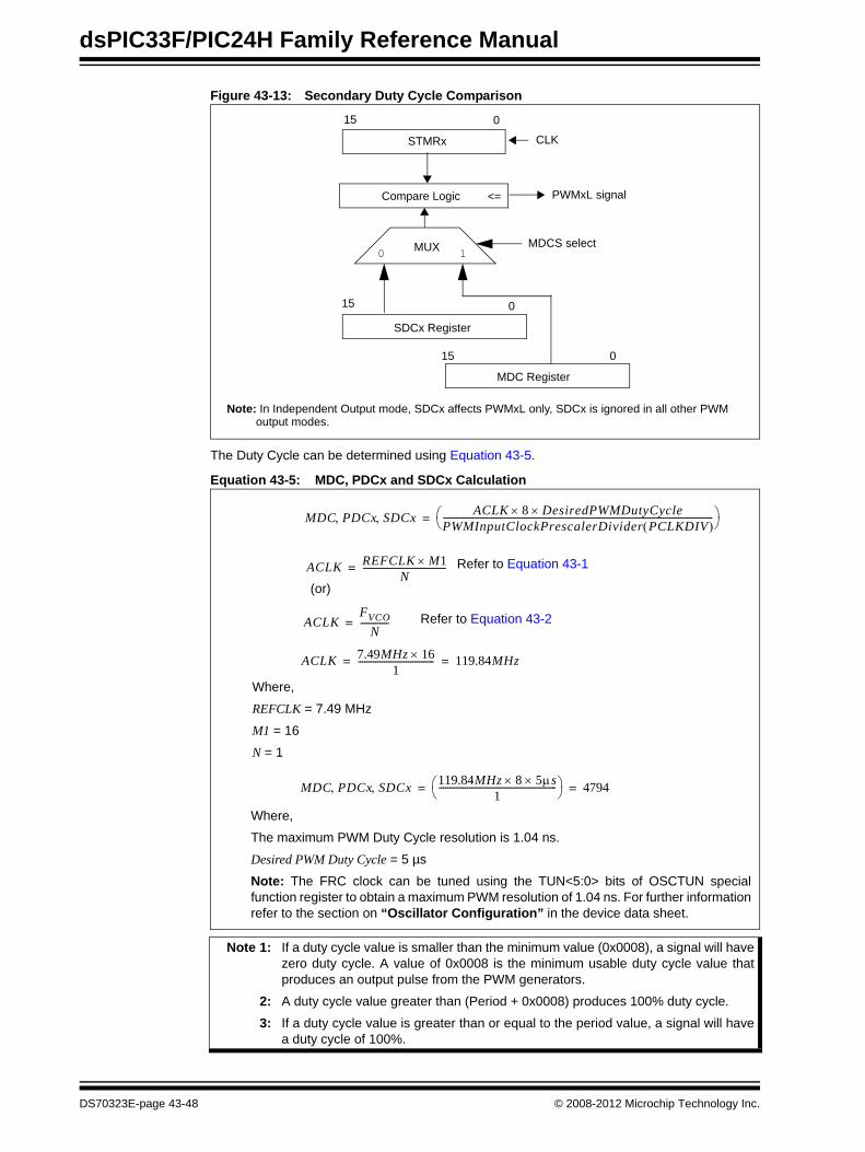
dsPIC33F/PIC24H Family Reference Manual
Figure 43-13: Secondary Duty Cycle Comparison
The Duty Cycle can be determined using Equation 43-5.
Equation 43-5: MDC, PDCx and SDCx Calculation
SDCx Register
STMRx
Compare Logic PWMxL signal
015
15
MUX
MDC Register
MDCS select0 1
CLK
15
0
0
<=
Note: In Independent Output mode, SDCx affects PWMxL only, SDCx is ignored in all other PWM output modes.
MDC PDCx SDCx, , ACLK 8× DesiredPWMDutyCycle×PWMInputClockPrescalerDivider PCLKDIV( )----------------------------------------------------------------------------------------------------------------------------⎝ ⎠⎛ ⎞=
ACLK REFCLK M1×N
--------------------------------------=
ACLK 7.49MHz 16×1
----------------------------------- 119.84MHz= =
(or)
Refer to Equation 43-1
ACLKFVCO
N-------------= Refer to Equation 43-2
Where,
REFCLK = 7.49 MHz
M1 = 16
N = 1
MDC PDCx SDCx, , 119.84MHz 8× 5μs×1
------------------------------------------------------⎝ ⎠⎛ ⎞ 4794= =
Where,
The maximum PWM Duty Cycle resolution is 1.04 ns.
Desired PWM Duty Cycle = 5 µs
Note: The FRC clock can be tuned using the TUN<5:0> bits of OSCTUN specialfunction register to obtain a maximum PWM resolution of 1.04 ns. For further informationrefer to the section on “Oscillator Configuration” in the device data sheet.
Note 1: If a duty cycle value is smaller than the minimum value (0x0008), a signal will havezero duty cycle. A value of 0x0008 is the minimum usable duty cycle value thatproduces an output pulse from the PWM generators.
2: A duty cycle value greater than (Period + 0x0008) produces 100% duty cycle.
3: If a duty cycle value is greater than or equal to the period value, a signal will havea duty cycle of 100%.
DS70323E-page 43-48 © 2008-2012 Microchip Technology Inc.

Section 43. High-Speed PWMH
igh-Speed PWM
43
Based on Equation 43-5, when the master, independent primary or independent secondary dutycycle is used, the register value is loaded in the MDC, PDCx or SDCx register, respectively. ThePWM duty cycle selection is shown in Example 43-12. The PWM duty cycle initialization is shownin Example 43-13.
Example 43-12: PWM Duty Cycle Selection
Example 43-13: PWM Duty Cycle Initialization
43.6.2.4 DUTY CYCLE RESOLUTION
When ACLK = 120 MHz, the PWM duty cycle and period resolution is 1.04 ns per LSb with thePWM clock configured for the highest prescaler setting. The PWM duty cycle bit resolution canbe determined using Equation 43-6:
Equation 43-6: Bit Resolution Calculation
The duty cycle bit resolution versus PWM frequencies at highest PWM clock frequency is shownin Table 43-1.
At the highest clock frequency, the clock period is 1.04 ns. The PWM resolution becomes coarserby configuring other PWM clock prescaler settings.
Table 43-1: PWM Frequency and Duty Cycle Resolution
PWM Duty Cycle Resolution PWM Frequency
16 bits 14.6 kHz15 bits 29.3 kHz14 bits 58.6 kHz13 bits 117.2 kHz12 bits 234.4 kHz11 bits 468.9 kHz10 bits 937.9 kHz9 bits 1.87 MHz8 bits 3.75 MHz
/* Select either Master Duty cycle or Independent Duty cycle */
PWMCON1bits.MDCS = 0; /* PDCX/SDCX provides duty cycle value */PWMCON1bits.MDCS = 1; /* MDC provides duty cycle value */
/* Initialize PWM Duty cycle value */
PDC1 = 4794;/* Independent Primary Duty Cycle is 5 µs from Equation 43-5 */SDC1 = 4794;/* Independent Secondary Duty Cycle is 5 µs from Equation 43-5 */MDC = 4794;/* Master Duty Cycle is 5 µs from Equation 43-5 */
BitResolution log2ACLK 8× DesiredPWMPeriod×
PWMInputClockPrescalerDivider PCLKDIV( )----------------------------------------------------------------------------------------------------------------------------⎝ ⎠⎛ ⎞×=
Where,
DesiredPWMPeriod 1DesiredPWMSwitchingFrequency-------------------------------------------------------------------------------------------⎝ ⎠⎛ ⎞=
© 2008-2012 Microchip Technology Inc. DS70323E-page 43-49

dsPIC33F/PIC24H Family Reference Manual
43.6.3 Dead Time GenerationDead time refers to a programmable period of time (specified by the Dead Time register (DTRx)or the Alternate Dead Time registers (ALTDTRx)), which prevents a PWM output from beingasserted until its complementary PWM signal has been deasserted for the specified time.
The High-Speed PWM module consists of four dead time control units. Each dead time controlunit has its own dead time value.
Dead time generation can be provided when any of the PWM I/O pin pairs are operating inComplementary PWM Output mode. Many power converter circuits require dead time becausepower transistors cannot switch instantaneously. To prevent current shoot-through, some amountof time must be provided between the turn-off event of one PWM output and the turn-on event ofthe other PWM output in a complementary pair or the turn-on event of the other transistor. The High-Speed PWM module provides the positive dead time and negative dead time. Thepositive dead time prevents overlapping of PWM outputs. Positive dead time generation isavailable for all output modes. Positive dead time circuitry works by blanking the leading edge ofthe PWM signal. Negative dead time is the forced overlap of the PWMxH and PWMxL signals.Negative dead time works when the extended time period of the currently active PWM outputoverlaps the PWM output that is just asserted. Certain converter techniques require a limitedamount of current shoot-through.
Negative dead time is specified only for complementary PWM signals. Negative dead time doesnot apply to user or current-limit, or fault overrides. This mode can be implemented by usingphase shift values in the PHASEx/SPHASEx registers that shift the PWM outputs so that theoutputs overlap another PWM signal from a different PWM output channel.
The dead time logic acts as a gate and allows an asserted PWM signal or an override value topropagate to the output. The dead time logic never asserts a PWM output on its own initiative.The dual dead time waveforms for dead time disabled, positive dead time and negative dead timeare illustrated in Figure 43-14.
Figure 43-14: Dual Dead Time Waveforms
The Dead Time feature can be disabled for each PWM generator. The dead time functionality iscontrolled by the Dead Time Control bits, DTC<1:0> (PWMCONx<7:6>). Dead time is notsupported for Independent PWM Output mode.
PWMxH
PWMxL
PWMxL
PWMxL
PWMxH
PWMxH
Dead Time Disabled
Positive Dead Time
DTRx ALTDTRx
Negative Dead Time
DS70323E-page 43-50 © 2008-2012 Microchip Technology Inc.

Section 43. High-Speed PWMH
igh-Speed PWM
43
43.6.4 Dead Time GeneratorsEach complementary output pair for the High-Speed PWM module has a 12-bit down counter toproduce the dead time insertion. Each dead time unit has a rising and falling edge detectorconnected to the duty cycle comparison output. Depending on whether the edge is rising orfalling, one of the transitions on the complementary outputs is delayed until the associated deadtime timer generates the specific delay period.
The dead time logic monitors the rising and falling edges of the PWM signals. The dead timecounters reset when the associated PWM signal is inactive and starts counting when the PWMsignal is active. Any selected signal source that provides the PWM output signal is processed bythe dead time logic.
The dead time can be determined using the formula shown in Equation 43-7:
Equation 43-7: Dead Time Calculation
Example 43-14:
There are three Dead Time Control modes:
• Positive Dead Time
Positive Dead Time mode describes a period of time when both the PWMxH and PWMxLoutputs are not asserted. This mode is useful when the application must allocate time todisable a power transistor prior to enabling other transistors. This is similar to a “Breakbefore Make” switch. When Positive Dead Time mode is specified, the DTRx registersspecify the dead time for the PWMxH output, and the ALTDTRx register specifies the deadtime for the PWMxL output.
• Negative Dead Time
Negative Dead Time mode describes a period of time when both the PWMxH and PWMxLoutputs are asserted. This mode is useful in current fed topologies that need to provide apath for current to flow when the power transistors are switching. This is similar to a “Makebefore Break” switch. When Negative Dead Time mode is specified, the DTRx registerspecifies the negative dead time for the PWMxL output, and the ALTDTRx register specifiesthe negative dead time for the PWMxH output. Negative dead time is specified only forcomplementary PWM output signals.
• Dead Time Disabled
Dead time logic can be disabled per PWM generator. The dead time functionality iscontrolled by the DTC<1:0> bits (PWMCONx<7:6>).
PWM Input Clock Prescaler Divider (PCLKDIV)
ACLK * 8 * DTRX, ALTDTRX = Desired Dead Time
Note: Maximum dead time resolution is 1.04 ns.
7.49 MHz1
* 16ACLK = = 119.84 MHz
Where,
M1 = 16REFCLK = 7.49 MHz
N = 1
DTRx , ALTDTRx =
Desired Dead Time = 100 ns
119.84 MHz1 * 8
= 96100 ns *
(Refer to Equation 43-1)
© 2008-2012 Microchip Technology Inc. DS70323E-page 43-51

dsPIC33F/PIC24H Family Reference Manual
43.6.5 Dead Time RangesThe dead time duration provided by each dead time unit is set by specifying an unsigned valuein the DTRx and ALTDTRx registers. At maximum operating clock frequency with a 1.04 ns dutycycle resolution, the dead time resolution is 1.04 ns. At the highest PWM resolution, themaximum dead time value is 17.03 µs.
43.6.6 Dead Time DistortionFor duty cycle values near 0% or 100%, the PWM signal becomes nonlinear if dead time isactive. For any duty cycle value less than the dead time, the PWM output is zero. For dutycycle values greater than (100% - dead time), the PWM output is same as if the duty cycleis (100% - dead time).
43.6.7 Dead Time ResolutionAt the highest clock rate, the dead time resolution is 1.04 ns under normal operating conditions.However, there are some exceptions: For fault current-limit, or user override events, the highestpossible dead time resolution is 8.32 ns (bit 3 in the DTRx and ALTDTRx registers) at maximumCPU speed and prescaler.
The configuration of PWM dead time control is shown in Example 43-15. The configuration ofPWM dead time initialization is shown in Example 43-16.
Example 43-15: PWM Dead Time Control
Example 43-16: PWM Dead Time Initialization
Note: When current-limit or fault override data is set to ‘0’, dead time is not applied, andthe “zero” override data is applied immediately.
Note: For duty cycle values greater than (100% - dead time), and the applicationdemands 100% duty cycle (that is, there is no dead time in the PWM output);therefore, configure DTC = 2 in the PWMCONx register.
/* Select Dead Time control *//* Choose one of these options */
PWMCON1bits.DTC = 0; /* Positive Dead Time applied for all modes */PWMCON1bits.DTC = 1; /* Negative Dead Time applied for all modes */
/* Dead Time value for PWM generator *//* Refer to Equation 43-7 */DTR1 = 96; /* Dead Time value is 100 ns */ALTDTR1 = 96; /* Alternate Dead time value is 100 ns */
DS70323E-page 43-52 © 2008-2012 Microchip Technology Inc.

Section 43. High-Speed PWMH
igh-Speed PWM
43
43.6.8 Dead Time Insertion in Center-Aligned ModeWhile using Center-Aligned mode and complementary PWM, only the ALTDTRx register mustbe used for dead time insertion. The dead time is inserted in the PWM waveform is illustrated inFigure 43-15.
Figure 43-15: Dead Time Insertion in Center-Aligned Mode
43.6.9 Phase ShiftPhase shift is the relative offset between PWMxH or PWMxL with respect to the master timebase. In Independent Output mode, the PHASEx register determines the relative phase shiftbetween PWMxH and the master time base. The SPHASEx register determines the relativephase shift between PWMxL and the master time base. The contents of the PHASEx register areused as an initialization value for the PTMRx register and the contents of SPHASEx register areused as an initialization value for the STMRx register.
Figure 43-16 and Figure 43-17 provide example waveforms for phase shifting in Complementarymode and Independent Output mode, respectively.
Note: With IUE = 1, all the three cases as described in 43.13 “Immediate Update ofPWM Duty Cycle” hold good in Center-aligned mode.
ALTDTRx ALTDTRx ALTDTRx ALTDTRx
PWMxH
PWMxL
PDCx
Period
2x Period
0
PHASEx
© 2008-2012 Microchip Technology Inc. DS70323E-page 43-53

dsPIC33F/PIC24H Family Reference Manual
Figure 43-16: Phase Shifting (Complementary Mode)
Figure 43-17: Phase Shifting (Independent Output Mode)
In addition, there are two shadow registers for the PHASEx and SPHASEx registers that areupdated whenever new values are written by the user-assigned application. These values aretransferred from the shadow registers to the PHASEx and SPHASEx registers on a Master timebase Reset. The actual application of these phase offsets on the PWM output occur on a mastertime base Reset. Figure 43-18 provides the timing diagram that illustrates how these events aregenerated.
The phase offset value can be any value between zero and the value in the PTPER register. AnyPHASEx or SPHASEx value greater than the PERIOD value is treated as a value equal to thePeriod. It is not possible to create phase shifts greater than the Period. Example 43-17 providesthe PWM phase shift initialization.
PWMxH without Phase Shift
PWMxH with Phase Shift
PWMxL without Phase Shift
PWMxL with Phase Shift
PHASEx
Note: In Complementary, Push-Pull and Redundant PWM Output modes, PHASEx controls the phase shift forPWMxH and PWMxL outputs.
PWMxH without Phase Shift
PWMxH with Phase Shift
PWMxL without Phase Shift
PWMxL with Phase Shift
Note: In Independent Output mode, SPHASEx controls the phase shift for PWMxL output, and PHASEx controls thephase shift for PWMxH output.
(different duty cycle)
PHASEx
SPHASEx
DS70323E-page 43-54 © 2008-2012 Microchip Technology Inc.

Section 43. High-Speed PWMH
igh-Speed PWM
43
Figure 43-18: Phase Shift Waveforms
Master Time Base
(PMTMR)
Period Match
Requested PHASEx
PHASEx
SPHASEx
PTMRx
PWMxH
STMRx
PWMxL
SDCx
PDCx
75 25
50 75 25
Note: Operation of High-Speed PWM module with independent time base is controlled by the master time base.
PTPER =100
PMTMR rollover on PTPER match
Next Phase Next Phase
Load PHASEx on MTB rollover
50
© 2008-2012 Microchip Technology Inc. DS70323E-page 43-55

dsPIC33F/PIC24H Family Reference Manual
Example 43-17: PWM Phase Shift Initialization
The bit resolution of PWM duty cycle, phase and dead time with respect to different input clockprescaler selections are shown in Table 43-2.
Table 43-2: Duty Cycle, Phase, Dead Time Bit Resolution Vs. Prescaler Selection
PWM Clock Prescaler
Bit Resolution
64 ns 32 ns 16 ns 8 ns 4 ns 2 ns 1 ns
1:1 bit 6 bit 5 bit 4 bit 3 bit 2 bit 1 bit 01:2 bit 5 bit 4 bit 3 bit 2 bit 1 bit 0 —1:4 bit 4 bit 3 bit 2 bit 1 bit 0 — —1:8 bit 3 bit 2 bit 1 bit 0 — — —1:16 bit 2 bit 1 bit 0 — — — —1:32 bit 1 bit 0 — — — — —1:64 bit 0 — — — — — —
/* Initialize phase shift value for the PWM output *//* Phase shifts are initialized when operating in Master Time Base */
PHASEx = 100; /* Primary phase shift value of 104 ns */
SPHASEx = 100; /* Secondary phase shift value of 104 ns */
DS70323E-page 43-56 © 2008-2012 Microchip Technology Inc.

Section 43. High-Speed PWMH
igh-Speed PWM
43
43.7 PWM TRIGGERSFor the ADC module, the TRIGx and STRIGx registers specify the triggering point for thePWMxH and PWMxL outputs, respectively. An ADC trigger signal is generated when theindependent time base counter (PTMRx or STMRx) register value matches with the specifiedTRIGx or STRIGx register value.
The Output Divider bits (TRGDIV<3:0>) in the PWM Trigger Control register (TRGCONx<15:12)act as a postscaler for the TRIGx register to generate ADC triggers. This allows the trigger signalto the ADC to be generated once for every 1, 2, 3.... and 16 trigger events. These bits specifyhow frequently the ADC trigger is generated.
Each PWM generator consists of the Trigger Postscaler Start Enable Select bits,TRGSTRT<5:0> (TRGCONx <5:0>), that specify how many PWM cycles to wait beforegenerating the first ADC trigger. The logic for ADC triggering by the High-Speed PWM module isillustrated in Figure 43-19.
Figure 43-19: PWM Trigger for Analog-to-Digital Conversion
Depending on the settings of the TRGDIV<3:0> bits (TRGCONx<15:12>) and theTRGSTRT<5:0> bits (TRGCONx <5:0>), triggers are generated at different PWM intervals, asillustrated in Figure 43-20 through Figure 43-27.
PTMRx
TRIGx
STMRx
STRIGx
1:1
1:16
1:1..
1:16
1
0
PWMx Trigger to ADCTRGSTRT
DTM
Clock
Clock
PWMxL Trigger to ADC
.
...
Delay TRGDIV
PWM Trigger Interrupt, PWMxH Trigger to ADCCMP
CMP
0
© 2008-2012 Microchip Technology Inc. DS70323E-page 43-57

dsPIC33F/PIC24H Family Reference Manual
Figure 43-20: PWM Trigger Signal in Relation to the PWM Output (TRGDIV = 0, TRGSTRT = 0)
Figure 43-21: PWM Trigger Signal in Relation to the PWM Output (TRGDIV = 0, TRGSTRT = 1)
PWMxH
TRIGx = 0
TRIGx = 8
TRIGx = 4808
TRIGx = 9616
1
PTPER = 9616
62 3 4 5 7
PWMxH
TRIGx = 0
TRIGx = 8
TRIGx = 4808
TRIGx = 9616
1
PTPER = 9616
62 3 4 5 7
DS70323E-page 43-58 © 2008-2012 Microchip Technology Inc.
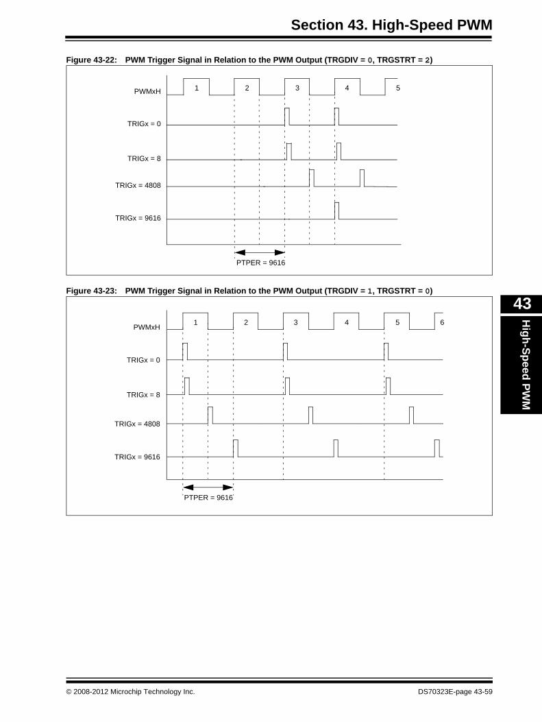
Section 43. High-Speed PWMH
igh-Speed PWM
43
Figure 43-22: PWM Trigger Signal in Relation to the PWM Output (TRGDIV = 0, TRGSTRT = 2)
Figure 43-23: PWM Trigger Signal in Relation to the PWM Output (TRGDIV = 1, TRGSTRT = 0)
PWMxH
TRIGx = 0
TRIGx = 8
TRIGx = 4808
TRIGx = 9616
1
PTPER = 9616
2 3 4 5
PWMxH
TRIGx = 0
TRIGx = 8
TRIGx = 4808
TRIGx = 9616
PTPER = 9616
51 2 3 4 6
© 2008-2012 Microchip Technology Inc. DS70323E-page 43-59

dsPIC33F/PIC24H Family Reference Manual
Figure 43-24: PWM Trigger Signal in Relation to the PWM Output (TRGDIV = 1, TRGSTRT = 1)
Figure 43-25: PWM Trigger Signal in Relation to the PWM Output (TRGDIV = 2, TRGSTRT = 0)
PWMxH
TRIGx = 0
TRIGx = 8
TRIGx = 4808
TRIGx = 9616
1
PTPER = 9616
62 3 4 5 7
PWMxH
TRIGx = 0
TRIGx = 8
TRIGx = 4808
TRIGx = 9616
1
PTPER = 9616
62 3 4 5 7
DS70323E-page 43-60 © 2008-2012 Microchip Technology Inc.

Section 43. High-Speed PWMH
igh-Speed PWM
43
Figure 43-26: PWM Trigger Signal in Relation to the PWM Output (TRGDIV = 2, TRGSTRT = 2)
Figure 43-27: PWM Trigger Signal in Relation to the PWM Output (TRGDIV = 2, TRGSTRT = 3)
The trigger divider allows the user-assigned application to tailor the ADC sample rates to therequirements of the control loop.
When the Dual Trigger Mode bit, DTM (TRGCONx<7>), is set to ‘1’, the ADC TRIGx output is aBoolean OR of the ADC trigger pulses for the TRIGx and the STRIGx time base comparisons.
The DTM mode of operation allows the user-assigned application to take two ADC samples onthe same pin within a single PWM cycle.
If ADC triggers are generated at a rate faster than the rate that the ADC can process, theoperation can result in loss of some samples. However, the user-assigned application canensure that the time it provides is enough to complete two ADC operations within a single PWMcycle.
The trigger pulse is generated regardless of the state of the Trigger Interrupt Enable bit, TRGIEN(PWMCONx<10>). If the TRGIEN bit (PWMCONx<10>) is set to ‘1’, an interrupt request (IRQ)is generated. The configuration of independent PWM ADC triggering is shown in Example 43-18.
PWMxH
TRIGx = 0
TRIGx = 8
TRIGx = 4808
TRIGx = 9616
1
PTPER = 9616
53 4 6 7
PWMxH
TRIGx = 0
TRIGx = 8
TRIGx = 4808
TRIGx = 9616
1
PTPER = 9616
64 5 7 8 9 10 11
Note: The secondary trigger comparison (STRIGx) does not generate PWM interruptsregardless of the state of the DTM bit (TRGCONx<7>).
© 2008-2012 Microchip Technology Inc. DS70323E-page 43-61

dsPIC33F/PIC24H Family Reference Manual
Example 43-18: Independent PWM ADC Triggering
Note 1: The TRGSTAT bit is cleared only by clearing the TRGIEN bit (PWMCONx<10>). Itis not cleared automatically.
2: Dynamic triggering can show some advantages where multiple PWM channels areused in applications such as IPFC and multi-phase buck regulators. TRIGx valuescan be changed based on the PWM period, duty, load current, etc. This is to ensurethat the trigger points are separated from the PWM channel’s rise and fallinstances.
/* Independent PWM ADC triggering */
TRIG1 = 1248; /* Point at which the ADC module is to betriggered by primary PWM */
STRIG1 = 2496; /* Point at which the ADC module is to betriggered by secondary PWM */
TRGCON1bits.TRGDIV = 0; /* Trigger output divider set to trigger ADC on every trigger match event */
TRGCON1bits.DTM = 1; /* Primary and Secondary triggers combined to create ADC trigger */
TRGCON1bits.TRGSTRT = 4; /* First ADC trigger event occurs after four trigger match events */
PWMCON1bits.TRGIEN = 1; /* Trigger event generates an interrupt request */
while (PWMCON1bits.TRGSTAT = = 1);/* Wait for PWM trigger interrupt statuschange */
DS70323E-page 43-62 © 2008-2012 Microchip Technology Inc.

Section 43. High-Speed PWMH
igh-Speed PWM
43
Figure 43-28: Effect of Phase Shift on PWM Triggers
When phase shifting the PWM signal, the PWM timer value is updated to reflect the new phasevalue. There is a possibility of missing trigger events when changing the phase from a smallervalue to a larger value. The user-assigned application must ensure that this does not affect anycontrol loop execution.
PTPER = 100
MasterTime Base(PMTMR)
RequestedPHASEx
PMTMR rollover on PTPER match
Next Phase Next Phase
(EIPU = 0) (EIPU = 0)
PTMRx = 50
PTMRx = 75
PTMRx = 50
PTMRx = 75
PTPER = 100
50
50
75 25
75 25PHASEx
PWM TimerPTMRx
Trigger event is missedwhen PHASEx is increased
6060
TRIGx = 60
PTMRx = 25
Load PHASEx on PTMRx rollover Load PHASEx on PTMRx rollover
60
TRIGx = 60 TRIGx = 60
Load PTMRx with PHASExon PMTMR rollover
Load PTMRx with PHASExon PMTMR rollover
Load PTMRx with PHASExon PMTMR rollover
© 2008-2012 Microchip Technology Inc. DS70323E-page 43-63

dsPIC33F/PIC24H Family Reference Manual
43.8 PWM INTERRUPTSThe High-Speed PWM module can generate interrupts based on internal timing signals orexternal signals through the current-limit and fault inputs. The primary time base module cangenerate an IRQ when a specified event occurs. Each PWM generator module provides its ownIRQ signal to the interrupt controller. The interrupt for each PWM generator is a Boolean OR ofthe trigger event IRQ, the current-limit input event, and the fault input event for that module.
Besides the individual PWM IRQs from each of the PWM generators, the interrupt controllerreceives an IRQ signal from the primary time base on special events.
The three IRQs coming from each PWM generator are called Individual PWM interrupts. The IRQfor each of the individual interrupts can come from the PWM individual trigger, PWM fault logic,or PWM current-limit logic. Each PWM generator consists of the PWM interrupt flag in an IFSxregister. When an IRQ is generated by any of the above sources, the PWM interrupt flagassociated with the selected PWM generator is set.
If more than one IRQ source is enabled, the interrupt source is determined using theuser-assigned application by checking the Trigger Interrupt Status bit, TRGSTAT(PWMCONx<13>), the Fault Interrupt Status bit, FLTSTAT (PWMCONx<15>), and theCurrent-Limit Interrupt Status bit, CLSTAT (PWMCONx<14>).
43.8.1 PWM Time Base InterruptsIn each PWM generator, the High-Speed PWM module can generate interrupts based on themaster time base and/or the individual time base. The SEVTCMP register specifies timer basedinterrupts for the primary time base, and the TRIGx registers specify timer based interrupts forthe individual time bases.
The primary time base special event interrupt is enabled through the SEIEN bit (PTCON<11>).In each PWM generator, the individual time base interrupts generated by the trigger logic arecontrolled by the TRGIEN bits (PWMCON<10>).
Note: When an appropriate match condition occurs, the Special Event Trigger signal andthe individual PWM trigger pulses to the ADC are always generated regardless ofthe setting of their respective interrupt enable bits.
DS70323E-page 43-64 © 2008-2012 Microchip Technology Inc.

Section 43. High-Speed PWMH
igh-Speed PWM
43
43.9 PWM OPERATING MODESThis section describes the following operation modes, which are supported by the High-SpeedPWM module:
• Push-Pull PWM Output Mode• Complementary PWM Output Mode• Redundant PWM Output Mode• True Independent PWM Output Mode
These operating modes can be selected using the PWM # I/O Pin Mode bits (PMOD<1:0>) in thePWM I/O Control register (IOCONx<11:10>).
43.9.1 Push-Pull PWM Output ModeIn Push-Pull PWM Output mode, the PWM outputs are alternately available on the PWMxH andPWMxL pins. Some typical applications of Push-Pull mode are provided in 43.16 “ApplicationInformation”. The PWM outputs in the Push-Pull PWM mode are illustrated in Figure 43-29.
Figure 43-29: Push-Pull PWM Output Mode
43.9.2 Complementary PWM Output ModeIn Complementary PWM Output mode, the PWM output PWMxH, is the complement of thePWMxL output. Some typical applications of Complementary PWM Output mode are providedin 43.16 “Application Information”.
The PWM outputs when the module operates in Complementary PWM Output mode areillustrated in Figure 43-30.
Figure 43-30: Complementary PWM Output Mode
PWM1H
PWM1L
DCX - DTRPeriod - DCX + DTR
TONTOFF
Period Period
Dead Time Dead Time Dead Time
Period
Duty Cycle
0
Period
TimerValue
Timer Resets
PWMxH
Value
PWMxL Duty Cycle
Duty Cycle Match
PWM1L
PWM1H
Dead Time(1) Dead Time(1) Dead Time(1)
Period
Period
Duty Cycle
0
Period
TimerValue
Timer Resets
PWMxH
Value
PWMxL (Period-duty cycle)
Duty Cycle Match
Note 1: Positive Dead Time is shown.
© 2008-2012 Microchip Technology Inc. DS70323E-page 43-65

dsPIC33F/PIC24H Family Reference Manual
43.9.3 Redundant PWM Output ModeIn Redundant PWM Output mode, the High-Speed PWM module has the ability to provide twocopies of a single-ended PWM output signal per PWM pin pair (PWMxH, PWMxL). This modeuses the PDCx register to specify the duty cycle. In this output mode, the two PWM output pinsprovide the same PWM signal unless the user-assigned application specifies an override value.Redundant PWM Output mode is illustrated in Figure 43-31.
Figure 43-31: Redundant PWM Output Mode
Table 43-3 provides the PWM register functionality for the PWM modes.
Table 43-3: Complementary, Push-Pull and Redundant PWM Output Mode Register Functionality
Time Base
Primary Master Time Base
Secondary Master Time Base(1) Independent Time Base
Function PWMxH PWMxL PWMxH PWMxL PWMxH PWMxL
PWM Period
PTPER PTPER STPER STPER PHASEx PHASEx
PWM Duty Cycle
MDC/PDCX MDC/PDCX MCD/PDCx MDC/PDCx MDC/PDCx MDC/PDCx
PWM Phase Shift
PHASEx PHASEx PHASEx PHASEx N/A N/A
ADC Trigger
SEVTCMP/TRIGx/STRIGx
SEVTCMP/TRIGx/STRIGx
SSEV-TCMP/TRI
Gx/STRIGx
SSEV-TCMP/TRI
Gx/STRIGx
SEVTCMP(2)
/SSEV-TCMP(2)/TRI
Gx/STRIGx
SEVTCMP(2)
/SSEV-TCMP(2)/TRI
Gx/STRIGx
Note 1: Refer to the specific device data sheet for the availability of Secondary Master Time Base.
2: Selection of trigger source as SEVTCMP or SSEVTCMP depends on the MTBS (PWMCONx<3>) bit setting. Refer to the specific device data sheet for the availability of MTBS bit.
Duty Cycle
0
Period
TimerValue
PWMxH
Value
Programmed
Duty Cycle
PWMxL
DS70323E-page 43-66 © 2008-2012 Microchip Technology Inc.

Section 43. High-Speed PWMH
igh-Speed PWM
43
43.9.4 True Independent PWM Output ModeIn True Independent PWM Output mode (PMOD = 11), the PWM outputs (PWMxH and PWMxL)can have different duty cycles. The PDCx register specifies the duty cycle for the PWMxH output,whereas the SDCx register specifies the duty cycle for the PWMxL output. In addition, thePWMxH and PWMxL outputs can either have different periods or they can be phase-shiftedrelative to each other.
• When ITB = 1, the PHASEx register specifies the PWM period for the PWMxH output and the SPHASEx register specifies the PWM period for the PWMxL output
• When ITB = 0, the PHASEx register specifies the phase shift for the PWMxH output and the SPHASEx register specifies the phase shift for the PWMxL output
Independent PWM Output mode is illustrated in Figure 43-32. PWM Output Pin mode selectionis shown in Example 43-19.
Figure 43-32: True Independent PWM Output Mode
Note: In Independent Time Base mode (ITB = 1), there may not be a deterministic phaserelationship between the PWMxH and PWMxL outputs.
Duty Cycle 2PWMxL
Duty Cycle 1PWMxH
Period
PMTMR = 0
Duty Cycle 2PWMxL
Duty Cycle 1PWMxH
Period
Phase 2
PMTMR = 0
Duty Cycle 2PWMxL
Duty Cycle 1
PWMxH
Period 2
Period 1
.
Master Time BasePhase = 0SPHASE = 0
Master Time Base
ITB = 1
with Phase Shift
© 2008-2012 Microchip Technology Inc. DS70323E-page 43-67

dsPIC33F/PIC24H Family Reference Manual
Example 43-19: PWM Output Pin Mode Selection
Table 43-4 provides the PWM register functionality for the Independent Output mode.
Table 43-4: Independent Output Mode Register Functionality
Table 43-5 provides the PMOD<1:0> bits selections for the different topologies and configuration.
/* Select PWM I/O pin Mode – Choose one of the following output modes */
IOCON1bits.PMOD = 0; /* For Complementary Output mode */
IOCON1bits.PMOD = 1; /* For Redundant Output mode */
IOCON1bits.PMOD = 2; /* For Push-Pull Output mode */
IOCON1bits.PMOD = 3; /* For True Independent Output mode */
Time Base Primary Master Time Base
Secondary Master Time Base(1) Independent Time Base
Function PWMxH PWMxL PWMxH PWMxL PWMxH PWMxL
PWM Period
PTPER PTPER STPER STPER PHASEx SPHASEx(2)
PWM Duty Cycle
MDC/PDCX MDC/SDCX MCD/PDCx MDC/PDCx MDC/PDCx MDC/SDCx
PWM Phase Shift
PHASEx SPHASEx(2) PHASEx SPHA-SEx(2)
N/A N/A
ADC Trigger
SEVTCMP/TRIGx/STRIGx
SEVTCMP/TRIGx/STRIGx
SSEV-TCMP/TRI
Gx/STRIGx
SSEV-TCMP/TRI
Gx/STRIGx
TRIGx STRIGx
Note 1: Refer to the specific device data sheet for the availability of Secondary Master Time Base.
2: The SPHASEx register is used only in Independent Output mode.
DS70323E-page 43-68 © 2008-2012 Microchip Technology Inc.

Section 43. High-Speed PWMH
igh-Speed PWM
43
Table 43-5: PMOD Bit Selection for Different Topologies and Configuration
Item Topology(1) Configuration PMOD<1:0>Setting
1 Flyback Converter True Independent Output mode/Redundant Output mode
11 or 01
2 Boost/PFC Converter True Independent Output mode/Redundant Output mode
11 or 01
3 Interleaved PFC Converter True Independent Output mode with Master Time Base
11
4 Forward Converter True Independent Output mode/Redundant Output mode
11 or 01
5 Double Ended Forward Converter
True Independent Output mode/Redundant Output mode
11 or 01
6 Active Clamp Forward Converter
Complementary PWM Output mode 00
7 LLC Half-Bridge Series Converter
Complementary PWM Output mode 00
8 Half-Bridge Converter Push-Pull PWM Output mode 10
9 Push-Pull Converter Push-Pull PWM Output mode 10
10 Full-Bridge Converter Push-Pull PWM Output mode 10
11 Phase Shifted Full-Bridge Converter
Complementary PWM Output mode 00
12 Single-Phase Synchronous Buck Regulator
Complementary PWM Output mode 00
13 Multi-Phase Synchronous Buck Regulator
Complementary PWM Output Mode with Master Time Base and Phase Staggering between each Buck converter PWM gate drives
00
Note 1: The listed topologies can be configured both in the voltage and in the current (i.e., Average and Peak Current) mode control.
© 2008-2012 Microchip Technology Inc. DS70323E-page 43-69

dsPIC33F/PIC24H Family Reference Manual
43.10 PWM FAULT PINSThe key functions of the PWM Fault input pins are as follows:
• For devices with re-mappable I/Os each PWM generator can select its fault input source from up to eight Fault sources (the input to each of the fault sources can be assigned as any of the re-mappable pins or the outputs of analog comparators using the virtual pins). To configure the analog comparator as one of the Fault sources, refer to 43.10.1 “PWM Fault Generated by the Analog Comparator”.
• For devices without re-mappable I/Os each PWM generator can select its fault input source from up to 23 Fault pins and up to four analog comparator outputs.
• Each PWM generator has Fault Control Signal Source Select bits (FLTSRC<4:0>) in the PWM Fault Current-Limit Control registers (FCLCONx<7:3>). These bits specify the source for its fault input signal.
• Each PWM generator has the Fault Interrupt Enable bit, FLTIEN (PWMCONx<12>). This bit enables the generation of fault IRQs.
• Each PWM generator has an associated Fault Polarity bit FLTPOL (FCLCONx<2>). This bit selects the active state of the selected fault input.
• Upon occurrence of a Fault condition, the PWMxH and PWMxL outputs can be forced to one of the following states:- If Independent Fault Mode bit, IFLTMOD(FCLCONx<15>) is enabled, the
FLTDAT<1:0> bits (High/Low) (IOCONx<5:4>) provides data values to be assigned to the PWMxH and PWMxL outputs. In this mode, the current limit source provides the fault input for PWMxH pin and Fault source provides the fault input for PWMxL pin and CLDAT<1:0> bits are ignored.
- In the Fault mode, the FLTDAT<1:0> bits (High/Low) (IOCONx<5:4>) provide the data values to be assigned to the PWMxH and PWMxL outputs.
The following list describes major functions of the fault input pin:
• A fault can override the PWM outputs. The Fault Override Data bits, (FLTDAT<1:0>) (IOCONx<5:4>) can have a value of either ‘0’ or ‘1’. If FLTDAT is set to ‘0’, it is processed asynchronously to enable the immediate shutdown of the associated power transistors in the application circuit. If FLTDAT is set to ‘1’, it is processed by the dead time logic and then applied to the PWM outputs.
• The fault signals can generate interrupts. The FLTIEN bit (PWMCONx<12>) controls the fault interrupt signal generation. The user-assigned application can specify interrupt signal generation even if the Fault Mode bits, FLTMOD<1:0> (FCLCONx<1:0>), disable the fault override function. This allows the fault input signal to be used as a general purpose exter-nal IRQ signal.
• The fault input signal that can be used as a trigger signal to the ADC, which initiates an ADC conversion process. The ADC trigger signals are always active regardless of the state of the High-Speed PWM module, the FLTMOD<1:0> bits (FCLCONx<1:0>), or the FLTIEN bit (PWMCONx<12>).
The FLTx pins are normally active-high. The FLTPOL bit (FCLCONx<2>), when set to ‘1’, invertsthe selected fault input signal; therefore, these pins are set as active-low.
The fault pins are also readable through the port I/O logic when the High-Speed PWM module isenabled. This allows the user-assigned application to poll the state of the fault pins in software.
DS70323E-page 43-70 © 2008-2012 Microchip Technology Inc.

Section 43. High-Speed PWMH
igh-Speed PWM
43
Figure 43-33: PWM Fault Control Module Block Diagram for Devices with Remappable I/O
FLTSRC<4:0>
FLT1
FLT2
FLT3
FLT4
FLT5
FLT6
FLT7
FLT8
00000
00001
00010
00011
00100
00111
00101
00110
0
1
PWMxH, PWMxL 2PWM
Generator #
FLTDAT<1:0> 2
PWMxH, PWMxL Signals2
FaultMode
SelectionLogic
FLTMOD<1:0>
Latch
Clear
FLTSTAT
PMTMR/SMTMR
© 2008-2012 Microchip Technology Inc. DS70323E-page 43-71

dsPIC33F/PIC24H Family Reference Manual
Figure 43-34: PWM Fault Control Module Block Diagram for Devices without Remappable I/O
FLTSRC<4:0>
CMP1x
CMP2x
CMP3x
CMP4x
FLT1
FLT2
FLT3
FLT4
FLT5
FLT6
FLT7
FLT8
00000
00001
00010
01000
01001
01010
01011
01100
01111
00011
01101
01110
Analog Comparator 1
Analog Comparator 2
Analog Comparator 3
Analog Comparator 4
Analog ComparatorModule
0
1
PWMxH, PWMxL 2
PWMGenerator #
FLTDAT<1:0> 2
PWMxH, PWMxL Signals2
FaultMode
SelectionLogic
FLTMOD<1:0>
Latch
Clear
FLTSTAT
PMTMR/SMTMR
FLT23 11110
Note: For more details on the available analog comparator outputs and Fault pins, refer to the specific device data sheet.
DS70323E-page 43-72 © 2008-2012 Microchip Technology Inc.

Section 43. High-Speed PWMH
igh-Speed PWM
43
43.10.1 PWM Fault Generated by the Analog Comparator
To use the comparator output as one of the fault/current-limit sources, remap the comparatoroutput to a general I/O (GPIO) pin and remap one of the external faults as an input to the samepin. Remapping can be to a GPIO pin or to a virtual pin.
Virtual pins are identical in functionality to all other RPx pins, with the exception of pinouts. Thefour virtual pins are internal to the devices and are not connected to a physical device pin. Thecomparator output remap to the virtual pin is illustrated in Figure 43-35.
For example, the output of the Analog Comparator and the PWM fault input can be configuredfor RP32. This configuration allows the Analog Comparator to trigger PWM faults without the useof actual physical pin on the device. Refer to the “I/O Ports” chapter in the specific device datasheet for more details on virtual pins.
Example 43-20 shows the configuration of the Analog Comparator 1 as one of the fault sourcesto the PWM that is connected to the fault input pin 1. The following output and input functions areused:
• Output Function: Analog Comparator 1• Input Function: PWM Fault Pin 1
Example 43-20: Configuring Analog Comparator as a Fault Source to the PWM
Figure 43-35: Comparator Output Remap to the Virtual Pin
Note: This section only applies to devices with remappable I/O. Refer to the ControllerFamily tables in the specific device data sheet for the list of available peripherals.For devices without remmappable I/O the analog comparators can be directlyassigned as fault source by configuring the FLTSRC<4:0> (FCLCONx<7:3>) bits asshown in Figure 43-34.
/* Unlock Registers */__builtin_write_OSCCONL(OSCCON & ~(1<<6));/* Configure Comparator Output Function */RPOR16bits.RP32R = 0b100111; /* Assign ACMP1 To Pin RP32 *//* Configure Fault Input Function */RPINR29bits.FLT1R=32; /* Assign Fault1 To Pin RP32 *//* Lock Registers */__builtin_write_OSCCONL(OSCCON | (1<<6));
Note: The comparator output can also be remapped to a general purpose I/O (GPIO) pin.
FLTSRC<4:0>/CLSRC<4:0>
CMP1x
00000
00001
00010
00100
00101
00110
00111
00011RPx
Analog Comparator Module
Virtual Pin
© 2008-2012 Microchip Technology Inc. DS70323E-page 43-73

dsPIC33F/PIC24H Family Reference Manual
43.10.2 Fault InterruptsThe FLTIENx bits (PWMCONx<12>) determine whether an interrupt will be generated when theFLTx input is asserted high. The FLTDAT<1:0> bits (High/Low) (IOCONx<5:4>) supply the datavalues to be assigned to the PWMxH and PWMxL pins in case of a fault.
The PWM Fault state is available on the Fault Interrupt Status bit, FLTSTAT (PWMCONx<15>).The FLTSTAT bit (PWMCONx<15>) displays the fault IRQ latch. If fault interrupts are notenabled, the FLTSTAT bit (PWMCONx<15>) displays the status of the selected FLTx input inpositive logic format. When the fault input pins are not used in association with a PWM generator,these pins can be used as general purpose I/O or interrupt input pins.
In addition to its operation as the PWM logic, the fault pin logic can also operate as an externalinterrupt pin. If the faults are not allowed to affect the PWM generators in the FCLCONx register,the fault pin can be used as a general purpose interrupt pin.
43.10.2.1 FAULT INPUT PIN MODES
The fault input pin consists of the following modes of operation:
• Latched mode: In Latched mode, the PWM outputs follow the states defined in the FLTDAT bits in the IOCONx registers when the fault pin is asserted. The PWM outputs remain in this state until the fault pin is deasserted and the corresponding interrupt flag is cleared in soft-ware. When both these actions occur and the appropriate fault exit sequence (as described in 43.10.4 “Fault Exit”) is followed the PWM outputs return to normal operation at the begin-ning of next PWM cycle boundary. If the FLTSTAT bit (PWMCONx<15>) is cleared before the Fault condition ends, the High-Speed PWM module waits until the fault pin is no longer asserted. Software can clear the FLTSTAT bit (PWMCONx<15>) by writing ‘0’ to the FLTIEN bit (PWMCONx<12>).
• Cycle-by-Cycle mode: In Cycle-by-Cycle mode, the PWM outputs remain in the deas-serted PWM state as long as the fault input pin remains asserted. In Complementary PWM Output mode, PWMxH is low (deasserted) and PWMxL is high (asserted). After the fault pin is driven high, the PWM outputs return to normal operation at the beginning of the following PWM cycle.
The operating mode for each fault input pin is selected using the FLTMOD<1:0>bits (FCLCONx<1:0>).
43.10.3 Fault EntryWith respect to the device clock signals, the PWM pins always provide asynchronous responseto the fault input pins. Therefore, if FLTDAT bits are deasserted(set to ‘0’) the PWM generatorwill immediately deassert the associated PWM outputs and if the specified FLTDAT bits areasserted (set to ‘1’), the FLTDAT<1:0> bits (High/Low) (IOCONx<5:4>) are processed by thedead time logic prior to being output as a PWM signal.
For more information on data sensitivity and behavior in response to the current-limit or Faultevents, refer to 43.12.4 “Fault/Current-Limit Override and Dead Time Logic”.
43.10.4 Fault ExitAfter a Fault condition has ended, the PWM signals must be restored at a PWM cycle boundaryto ensure proper synchronization of PWM signal edges and manual signal overrides.
If Cycle-by-Cycle Fault mode is selected, the fault is automatically reset on every PWM cycle. Noadditional coding is needed to exit the Fault condition.
For Latched Fault mode, the following sequence must be followed to exit the Fault condition:
1. Poll the PWM Fault source to determine if the fault signal has been deasserted.2. Set the OVRDAT<1:0> (IOCONx<7:6>) bits to ‘0’.3. Enable overrides for PWMxH and PWMxL by setting the OVRENH (IOCONx<9>) and
Note: In RPx, if x = 32, 33, 34 or 35, the comparator output is remapped to a virtual pin,which is unavailable to the user.
DS70323E-page 43-74 © 2008-2012 Microchip Technology Inc.

Section 43. High-Speed PWMH
igh-Speed PWM
43
OVRENL(IOCONx<8>) to high.4. Disable the PWM fault by setting FLTMOD<1:0> bits (FCLCONx<1:0>) = ‘0b11.5. Provide a delay of at least 1 PWM cycle.6. Enable the PWM fault by setting FLTMOD<1:0> bits (FCLCONx<1:0>) =‘0b00.7. If PWM Fault interrupt is enabled then perform the following sub-steps and then proceed
to step 8. If not then skip this step and proceed to step 8.- a) Complete the PWM fault Interrupt Service Routine.- b) Disable the PWM fault interrupt by clearing the FLTIEN bit (PWMCONx<12> = 0.- c) Enable the PWM fault interrupt by setting the FLTIEN bit (PWMCONx<12>) = 1.
8. Disable the override by clearing the OVRENH (IOCONx<9>) and OVRENL (IOCONx<8>)bits.
43.10.5 Fault Exit with PMTMR DisabledThere is a special case for exiting a Fault condition when the PWM time base isdisabled (PTEN = 0). When a fault input is programmed for Cycle-by-Cycle mode, the PWMoutputs are immediately restored to normal operation when the fault input pin is deasserted. ThePWM outputs should return to their default programmed values. When a fault input isprogrammed for Latched mode, the PWM outputs are restored immediately when the fault inputpin is deasserted and the FLTSTAT bit (PWMCONx<15>) is cleared in software.
43.10.6 Fault Pin Software ControlThe fault pin can be controlled manually in software. Since the fault input is shared with a GPIOport pin, this pin can be configured as an output by clearing the corresponding TRIS bit. Whenthe port bit for the GPIO pin is set, the fault input will be activated.
© 2008-2012 Microchip Technology Inc. DS70323E-page 43-75

dsPIC33F/PIC24H Family Reference Manual
43.10.7 PWM Current-Limit PinsThe key functions of the PWM current-limit pins are as follows:
• For devices with re-mappable I/Os each PWM generator can select its current-limit input source from up to eight Fault sources (the input to each of the fault sources can be assigned as any of the re-mappable pins or the outputs of analog comparators using the virtual pins). To configure the analog comparator as one of the current-limit sources, refer to 43.10.1 “PWM Fault Generated by the Analog Comparator”.
• For devices without re-mappable I/Os each PWM generator can select its current-limit input source from up to 23 Fault pins and up to four analog comparator outputs.
• Each PWM generator has Current-Limit Control Signal Source Select bits CLSRC<4:0> (FCLCONx<14:10>). These bits specify the source for its current-limit signal.
• Each PWM generator has a corresponding Current-Limit Interrupt Enable bit, CLIEN (PWMCONx<11>). This bit enables the generation of current-limit IRQs.
• Each PWM generator has an associated Current-Limit Polarity bit, CLPOL (FCLCONx<9>).• Upon occurrence of current-limit condition, outputs of the PWMxH and PWMxL generator
change to one of the following states:- If the Independent Fault Enable bit, IFLTMOD (FCLCONx<15>) is set, the
CLDAT<1:0> bits (IOCONx<3:2>) are not used for override functions.- If the IFLTMOD bit (FCLCONx<15>) is clear, and the CLMOD bit (FCLCONx<8>) is
set, enabling the current-limit function, then the CLDAT<1:0> bits (High/Low) (IOCONx<3:2>) supply the data values to be assigned to the PWMxH and PWMxL outputs when a current limit is active.
The major functions of the current-limit pin are as follows:
• A current-limit can override the PWM outputs. The CLDAT<1:0> bits (IOCONx<3:2>) can have a value of either ‘0’ or ‘1’. If CLDAT is set to ‘0’, it is processed asynchronously to enable immediate shutdown of the associated power transistors in the application circuit. If CLDAT is set to ‘1’, it is processed by the dead time logic and then applied to the PWM outputs.
• The current-limit signals can generate interrupts. The CLIEN bit (PWMCONx<11>) controls the current-limit interrupt signal generation. The user-assigned application can specify interrupt generation even if the CLMOD bit (FCLCONx<8>) disables the current-limit override function. This allows the current-limit input signal to be used as a general purpose external IRQ signal.
• The current-limit input signal that can be used as a trigger signal to the ADC, which initiates an ADC conversion process. The ADC trigger signals are always active regardless of the state of the High-Speed PWM module, the FLTMOD<1:0> bits (FCLCONx<1:0>), or the FLTIEN bit (PWMCONx<12>).
DS70323E-page 43-76 © 2008-2012 Microchip Technology Inc.
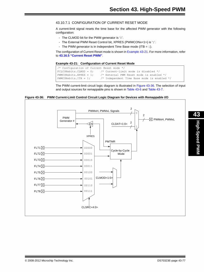
Section 43. High-Speed PWMH
igh-Speed PWM
43
43.10.7.1 CONFIGURATION OF CURRENT RESET MODE
A current-limit signal resets the time base for the affected PWM generator with the followingconfiguration:
- The CLMOD bit for the PWM generator is ‘0’.- The External PWM Reset Control bit, XPRES (PWMCONx<1>) is ‘1’.- The PWM generator is in Independent Time Base mode (ITB = 1).
The configuration of Current Reset mode is shown in Example 43-21. For more information, referto 43.16.5 “Current Reset PWM”.
Example 43-21: Configuration of Current Reset Mode
The PWM current-limit circuit logic diagram is illustrated in Figure 43-36. The selection of inputand output sources for remappable pins is shown in Table 43-6 and Table 43-7.
Figure 43-36: PWM Current-Limit Control Circuit Logic Diagram for Devices with Remappable I/O
/* Configuration of Current Reset mode */FCLCONxbits.CLMOD = 0; /* Current-limit mode is disabled */PWMCONxbits.XPRES = 1; /* External PWM Reset mode is enabled */PWMCONxbits.ITB = 1; /* Independent Time Base mode is enabled */
CLSRC<4:0>
FLT1
FLT2
FLT3
FLT4
FLT5
FLT6
FLT7
FLT8
00000
00001
00010
00011
00100
00111
00101
00110
0
1
PWMxH, PWMxL 2
PWMGenerator #
CLDAT<1:0> 2
PWMxH, PWMxL Signals2
Cycle-by-CycleMode
PMTMR
CLMOD<1:0>
EN
XPRES
© 2008-2012 Microchip Technology Inc. DS70323E-page 43-77

dsPIC33F/PIC24H Family Reference Manual
Figure 43-37: PWM Current-Limit Control Circuit Logic Diagram for Devices without Remappable I/O
0
1
PWMxH, PWMxL 2
PWMGenerator #
CLDAT<1:0> 2
PWMxH, PWMxL Signals2
Cycle-by-CycleMode
PMTMR/SMTMR
CLMOD<1:0>
EN
XPRES
CLSRC<4:0>
CMP1x
CMP2x
CMP3x
CMP4x
FLT1
FLT2
FLT3
FLT4
FLT5
FLT6
FLT7
FLT8
00000
00001
00010
01000
01001
01010
01011
01100
01111
00011
01101
01110
Analog Comparator 1
Analog Comparator 2
Analog Comparator 3
Analog Comparator 4
Analog ComparatorModule
FLT23 11110
DTCMPx
FLT9 10000
DS70323E-page 43-78 © 2008-2012 Microchip Technology Inc.

Section 43. High-Speed PWMH
igh-Speed PWM
43
Table 43-6: Selectable Input Sources (Maps Input to Function) for Devices with Remappable I/O
Table 43-7: Output Selection for Remappable Pin (RPn) for Devices with Remappable I/O
43.10.7.2 CONFIGURING ANALOG COMPARATOR IN CYCLE-BY-CYCLE MODE
The built-in High-Speed Analog Comparator can be configured to set the Cycle-by-Cycle mode.The typical configuration of Analog Comparator in Cycle-by-Cycle mode is illustrated inFigure 43-38.
Figure 43-38: Digital Peak Current Mode Boost Converter
Input Name Function Name Register Configuration Bits
PWM Fault Input 1 FLT1 RPINR29 FLT1R<5:0>
PWM Fault Input 2 FLT2 RPINR30 FLT2R<5:0>
PWM Fault Input 3 FLT3 RPINR30 FLT3R<5:0>
PWM Fault Input 4 FLT4 RPINR31 FLT4R<5:0>
PWM Fault Input 5 FLT5 RPINR31 FLT5R<5:0>
PWM Fault Input 6 FLT6 RPINR32 FLT6R<5:0>
PWM Fault Input 7 FLT7 RPINR32 FLT7R<5:0>
PWM Fault Input 8 FLT8 RPINR33 FLT8R<5:0>
Function RPORn<5:0> Output Name
ACMP1 100111 RPn tied to Analog Comparator Output 1
ACMP2 101000 RPn tied to Analog Comparator Output 2
ACMP3 101001 RPn tied to Analog Comparator Output 3
ACMP4 101010 RPn tied to Analog Comparator Output 4
EXTREF
Faul
t Sou
rce
CMREF
Targeted Voltage
PI ADC
High-Speed PWM
Virtual I/O(1)
DAC
MUX
Comp
INTREF
Control
AVDD/2
D VBoostL
IS
PWMxH/
R
SR
R
VIN +
VIN -
Slope Compensation
dsPIC33FJXXGSXXX
Note 1: Applicable only to devices with re-mappable I/O.
PWMxL
© 2008-2012 Microchip Technology Inc. DS70323E-page 43-79

dsPIC33F/PIC24H Family Reference Manual
The analog comparator provides high-speed operation with a typical delay of 20 ns. The positiveinput of the comparator is connected to an analog multiplexer (INSEL<1:0>) in the CMPCONxregister. The positive input of the comparator measures the current signal (voltage signal).
The negative input of the comparator is always connected to the DAC circuit. For moreinformation, refer to Figure 45-1 in Section 45. “High-Speed Analog Comparator” (DS70296).
The typical DAC settling time is 650 ns. The DAC settling time is measured when Range = 1 (highrange) and CMREF<9:0> transitions from 0x1FF to 0x300. Each analog comparator has adedicated 10-bit DAC that is used to program the comparator threshold voltage.
The DAC range can be selected using ‘RANGE’ in the Comparator Control register (CMPCONx).The dsPIC33F “GS” series devices with remappable I/O support four virtual RPn pins (RP32,RP33, RP34 and RP35) that are identical in functionality to all other RPn pins, with the exceptionof pinouts. Refer to the “I/O Ports” chapter in the specific device data sheet for more information.
These pins provide a simple way for inter-peripheral connection without utilizing a physical pin.For example, the output of the analog comparator can be connected to RP32 and the PWM FaultSource (FLT1) can also be configured for RP32. The virtual pin configuration is shownin Example 43-22.
Example 43-22: Virtual Pin Configuration for Devices with Remappable I/O
43.10.8 Current-Limit InterruptsThe state of the PWM current-limit conditions is available on the CLSTAT bit (PWMCONx<14>).The CLSTAT bits display the current-limit IRQ flag if the CLIEN bit (PWMCONx<11>) is set. Ifcurrent-limit interrupts are not enabled, the CLSTAT bits display the status of the selectedcurrent-limit inputs in positive logic format. When the current-limit input pin associated with aPWM generator is not used, these pins can be used as general purpose I/O or interrupt inputpins.
The current-limit pins are normally active-high. If set to ‘1’, the CLPOL bit (FCLCONx<9>) invertsthe selected current-limit input signal and drives the signal into active-low state.
The interrupts generated by the selected current-limit signals are combined to create a singleIRQ signal. This signal is sent to the interrupt controller, which has its own interrupt vector,interrupt flag bit, interrupt enable bit and interrupt priority bits associated with it.
The fault pins are also readable through the port I/O logic when the High-Speed PWM module isenabled. This capability allows the user-assigned application to poll the state of the fault pins insoftware.
43.10.9 Simultaneous PWM Faults and Current-LimitsThe current-limit override function, if enabled and active, forces the PWMxH and PWMxL pins toread the values specified by the CLDAT<1:0> bits (IOCONx<3:2>), unless the Fault function isenabled and active. If the selected fault input is active, the PWMxH and PWMxL outputs read thevalues specified by the FLTDAT<1:0> bits (IOCONx<5:4>).
RPINR29bits.FLT1R = 0b100000; /* Fault Source(FLT1) connected to RP32 */
RPOR16bits.RP32R = 0b100111; /* Output of the analog computer 1 connectedto RP32 */
DS70323E-page 43-80 © 2008-2012 Microchip Technology Inc.

Section 43. High-Speed PWMH
igh-Speed PWM
43
43.10.10 PWM Fault and Current-Limit Trigger Outputs to ADCThe CLSRC<4:0> bits (FCLCONx<14:10>) and FLTSRC<4:0> bits (FCLCONx<7:3>) andcontrol the fault selection to each PWM generator module. The control multiplexers select thedesired fault and current-limit signals for their respective modules. The selected fault andcurrent-limit signals which are also available to the ADC module as trigger signals, initiate ADCsampling and conversion operations. The configuration of PWM fault, current-limit andleading-edge blanking is shown in Example 43-23.
Example 43-23: PWM Fault, Current-Limit and Leading-Edge Blanking Configuration/* PWM Fault, Current-Limit, and Leading-Edge Blanking Configuration */
//FCLCON1bits.IFLTMOD = 0; /* CLDAT bits and FLTDAT bits control PWMxH/PWMxL pins on occurrence of current limit and fault inputs respectively */
//FCLCON1bits.CLSRC = 0; /* Fault 1 is selected as source for the Current Limit Control signal *///FCLCON1bits.FLTSRC = 3; /* Fault 4 is selected as source for the Fault Control Signal source *///FCLCON1bits.CLPOL = 1; /* Current-limit source is active-low *///FCLCON1bits.FLTPOL = 1; /* Fault Input source is active-low *///FCLCON1bits.CLMOD = 1; /* Enable current-limit function *///FCLCON1bits.FLTMOD = 1; /* Enable Cycle-by-Cycle Fault mode */
FCLCON1 = 0x031D;
IOCON1bits.FLTDAT = 0; /* PWMxH and PWMxL are driven inactive on occurrence of fault */IOCON1bits.CLDAT = 0; /* PWMxH and PWMxL are driven inactive on occurrence of current-limit */
//LEBCON1bits.PHR = 1; /* Rising edge of PWMxH will trigger LEB counter *///LEBCON1bits.PHF = 0; /* Falling edge of PWMxH is ignored by LEB counter *///LEBCON1bits.PLR = 1; /* Rising edge of PWMxL will trigger LEB counter *///LEBCON1bits.PLF = 0; /* Falling edge of PWMxL is ignored by LEB counter *///LEBCON1bits.FLTLEBEN = 1; /* Enable fault LEB for selected source *///LEBCON1bits.CLLEBEN = 1; /* Enable current-limit LEB for selected source *///LEBCON1bits.LEB = 8; /* Blanking period of 8.32 ns */
LEBCON1 = 0xAC40;
PWMCON1bits.XPRES = 0; /* External pins do not affect PWM time base reset */PWMCON1bits.FLTIEN = 1; /* Enable fault interrupt */PWMCON1bits.CLIEN = 1; /* Enable current-limit interrupt */
Note: The code in Example 43-23 applies to devices with remappable I/O only.
© 2008-2012 Microchip Technology Inc. DS70323E-page 43-81

dsPIC33F/PIC24H Family Reference Manual
43.11 SPECIAL FEATURESThe following special features are available in the High-Speed PWM module:
• Leading-Edge Blanking (LEB)• Individual time base capture• PWM pin swapping • PWM output pin control and override• PWM immediate update
43.11.1 Leading-Edge Blanking (LEB)Each PWM generator supports LEB of the current-limit and fault inputs through the LEB<6:0>bits (LEBCONx<9:3>) and the PHR (LEBCONx<15>), PHF (LEBCONx<14>),PLR (LEBCONx<13>), PLF (LEBCONx<12>, FLTLEBEN (LEBCONx<11>) andCLLEBEN (LEBCONx<10>) bits in the Leading-Edge Blanking Control registers. The purposeof LEB is to mask the transients that occur on the application printed circuit board when thepower transistors are turned ON and OFF.
The LEB<6:0> bits (LEBCONx<9:3>) are edge-sensitive, and support the blanking (ignoring) ofthe current-limit and fault inputs for a period of 0 ns to 1057 ns in 8.32 ns increments followingany specified rising or falling edge of the PWMxH and PWMxL signals.
Equation 43-8: LEB Calculation for Devices without Remappable I/O
Equation 43-9: LEB Calculation for Devices with Remappable I/O
In High-Speed Switching applications, switches (such as MOSFETs/IGBTs) typically generatevery large transients. These transients can cause problematic measurement errors. The LEBfunction enables the user-assigned application to ignore the expected transients caused by theMOSFETs/IGBTs switching that occurs near the edges of the PWM output signals.
The PHR bit (LEBCONx<15>), PHF bit (LEBCONx<14>), PLR bit (LEBCONx<13>) and PLFbit (LEBCONx<12>) select the edge type of the PWMxH and PWMxL signals, which starts theblanking timer. If a new selected edge triggers the LEB timer while the timer is still active from apreviously selected PWM edge, the timer reinitializes and continues counting.
The FLTLEBEN bit (LEBCONx<11>) and the CLLEBEN bit (LEBCONx<10>) enable theapplication of the blanking period to the selected fault and current-limit inputs. Figure 43-39illustrates how an application ignores the fault signal in the specified blanking period.
On devices with the LEB Version 2 register, it is possible to specify periods of time where thecurrent-limit and/or Fault signal is entirely ignored. The BCH, BCL, BPHH, BPHL, BPLH andBPLL bits in the LEBCONx register select the PWMxH, PWMxL and/or CHOP clock signals asthe source of the state blanking function. It is also possible to blank the selected Fault orcurrent-limit signal when the PWMxH output is high and/or low, and if the PWMxL is high and/orlow. The PWM State Blank Source Select bits (BLANKSEL<3:0>) in the PWM Auxiliary Controlregister (AUXCONx<11:8>) select the PWM generator used as the blanking signal source.
Note: Refer to the “High-Speed PWM” chapter in the specific device data sheet todetermine the LEB version that is available for your device.
LEB Duration @ Maximum Clock Rate = (LEBDLYx<8:0>) * 8.32 ns
LEB Duration @ Maximum Clock Rate = (LEBCONx<6:0>) * 8.32 ns
DS70323E-page 43-82 © 2008-2012 Microchip Technology Inc.

Section 43. High-Speed PWMH
igh-Speed PWM
43
Figure 43-39: Leading-Edge Blanking
43.11.2 Individual Time Base CaptureEach PWM generator has a Primary PWM Time Base Capture register (PWMCAPx) thatautomatically captures the independent time base counter value when the rising edge of thecurrent-limit signal is detected. This feature is active only after the application of the LEB function.The user-assigned application should read the register before the next PWM cycle causes thecapture register to be updated again.The Capture register is used in current-limit PWM control applications that use the analogcomparators or external circuitry to terminate the PWM duty cycle or period. By reading theindependent time base value at the current threshold, the user-assigned application cancalculate the slope of the current rise in the inductor. The secondary independent time base doesnot have an associated Capture register.
43.11.3 Dead-Time CompensationIn AC motor control applications, when the dead time is applied to the PWM signals, thetransistors are disabled. During the dead time, motor current continues to flow through therecirculating diodes, but the applied voltage is zero. The zero applied voltage during dead timecauses a distortion of the desired voltage waveform and subsequently, a motor current distortion.This distortion causes torque variations that can affect the stability of the control system and theperformance of the motor. When Dead-Time Compensation mode is selected through theDTC<1:0> bits (PWMCONx<7:6>), an external input signal, DTCMPx, will cause the value in theDTRx register to be added to, or subtracted from, the duty cycle specified by the MDC/PDCxregisters. The ALTDTRx register will specify the dead-time period for both the PWMxH andPWMxL output signals. Dead-time compensation is available only for Positive Dead-Time mode.Negative dead times are not supported with compensation. Figure 43-40 illustrates thedead-time compensation timing diagram.
Switching Noise
Blanking time is determined by theLEB<9:3> bits in the LEBCONx registers
Fault and current-limitcircuitry ignores theswitching noise
PWM Output
High Power Signal
Blanking Signal
Power signal as seenby fault circuitry
© 2008-2012 Microchip Technology Inc. DS70323E-page 43-83

dsPIC33F/PIC24H Family Reference Manual
Figure 43-40: Dead-Time Compensation
43.11.4 Chop ModeMany power control applications use transistor configurations that require an isolated transistorgate drive. An example is a three-phase “H-bridge” configuration, where the upper transistors areat an elevated electrical potential.
One method to achieve an isolated gate drive circuit is to use pulse transformers to couple thePWM signals across a galvanic isolation barrier to the transistors. Unfortunately, in applicationsthat use either long duty cycle ratios, or slow PWM frequencies, the transformer’s low-frequencyresponse is poor. The pulse transformer cannot pass a long duration PWM signal to the isolatedtransistor(s). If the PWM signals are “chopped” or gated by a high-frequency clock signal, thehigh-frequency alternating signal easily passes through the pulse transformer. The choppingfrequency is typically hundreds or thousands of times higher in frequency as compared to thePWM frequency. The higher the chopping (carrier) frequency relative to the PWM frequency, themore the PWM duty cycle resolution is preserved.
Figure 43-41 illustrates an example waveform of high-speed PWM chopping. In this example,a 20 kHz PWM signal is chopped with a 500 kHz carrier generated by the chop clock.
Note: Dead-time compensation only applies to Complementary PWM Output mode.Specifying dead-time compensation in any other PWM Output mode will yieldunpredictable results.
Normal PWM
Stretched PWM through DTR
Shortened PWM through DTR
DTCMPx selected PWMxH
Create PWMxL
PWMxH with ALDTR Dead Time
PWMxL with ALDTR Dead Time
DS70323E-page 43-84 © 2008-2012 Microchip Technology Inc.

Section 43. High-Speed PWMH
igh-Speed PWM
43
Figure 43-41: High-Frequency PWM Chopping
The chopping function performs a logical AND operation of the PWM outputs. Because of thefinite period of the chopping clock, the resultant PWM duty cycle resolution is limited to one halfof the chop clock period.
The PWM Chop Clock Generator register (CHOP) enables the user to specify a chopping clockfrequency. The CHOP value specifies a PWM clock divide ratio. The chop clock divider operatesat the PWM clock frequency specified by the PCLKDIV<2:0> bits (PTCON2<2:0>). TheCHPCLKEN bit in the CHOP register enables the chop clock generator.
The PWMxH Output Chopping Enable bit, CHOPHEN (AUXCONx<1>), and the PWMxL OutputChopping Enable bit, CHOPLEN (AUXCONx<0>), enable the chop clock to be applied to thePWM outputs. The PWM Chop Clock Source Select bits, CHOPSEL<3:0> (AUXCONx<5:2>)select the desired source for the chop clock. The default selection is the chop clock generatorcontrolled by the CHOP register. The CHOPSEL<3:0> bits (AUXCONx<5:2>) enable the user toselect other PWM generators as a chop clock source.
If the CHOPHEN bit (AUXCONx<1>) or the CHOPLEN bit (AUXCONx<0>) is set, the choppingfunction is applied to the PWM output signals after the current-limit and Fault functions areapplied to the PWM signal. The CHPCLK signal is available for output from the module for useas an output signal for the device.
Normally, the chopping clock frequency is higher than the PWM cycle frequency, but newapplications can use chop clock frequencies that are much lower than the PWM cycle frequency.Figure 43-42 illustrates a low-frequency PWM chopping waveform. In this figure, another PWMgenerator operating at a lower frequency chops or “blanks” the PWM signal.
Figure 43-42: Low-Frequency PWM Chopping
50 μsec
Unchopped PWM
Chopping Signal
Chopped PWM
1 μsec
Note: Not drawn to scale.
50 ms
Chopping Signal
Unchopped PWM
Chopped PWM
Note: Not drawn to scale.
1 μsec
© 2008-2012 Microchip Technology Inc. DS70323E-page 43-85

dsPIC33F/PIC24H Family Reference Manual
43.11.5 PWM Pin SwappingThe SWAP PWMxH and PWMxL Pins bit, SWAP (IOCONx<1>), if set to ‘1’, enables theuser-assigned application to connect the PWMxH signal to the PWMxL pin and the PWMxLsignal to the PWMxH pin. If the SWAP bit (IOCONx<1>) is set to ‘0’, the PWM signals areconnected to their respective pins. To perform the swapping function on the PWM cycle boundaries, the Output OverrideSynchronization bit, OSYNC (IOCONx<0>), must be set. If the user-assigned applicationchanges the state of the SWAP bit (IOCONx<1>) when the module is operating and the OSYNCbit (IOCONx<0>) is clear, the SWAP function attempts to execute in the middle of a PWM cycleand the operation yields unpredictable results. The SWAP function must be executed prior to the application of dead time. Dead time processingis required since execution of switch function can enable the transistors in the user-assignedapplication that are previously in disable state, possibly causing current shoot-through.The SWAP feature is useful for the applications that support multiple switching topologies with asingle application circuit board. It also enables the user-assigned application to change thetransistor modulation scheme in response to changing conditions.The SWAP function can be implemented by using either of the following methods:• Dynamic Swapping: In the dynamic swapping, the state of the SWAP bit can be changed
dynamically based on the system response (for example, SMPS Power Control).• Static Swapping: In static swapping, the SWAP bit is set during the start-up configuration
and remains unchanged during the program execution or on-the-fly (for example, Motor Control).
43.11.5.1 EXAMPLE 1: PIN SWAPPING WITH SMPS POWER CONTROL
The SMPS Power Control example describes dynamic swapping. In power conversionapplications, the transistor modulation technique can be changed between the full-bridge ZeroVoltage Transition (ZVT) and standard full-bridge “on-the-fly” transition to meet different load andefficiency requirements. The generic full-bridge converter as illustrated in Figure 43-43, canoperate in Push-Pull mode. The transistors are configured as follows:
• Q1 = Q4 • Q2 = Q3The generic full-bridge converter can also operate in ZVT mode. The transistors are configuredas follows:
• Q1 = PWM1H• Q2 = PWM1L• Q3 = PWM2H• Q4 = PWM2L
Figure 43-43: SMPS Power Control
+
T1 VOUT
+VIN
Q1
Q2Q4
Q3
DS70323E-page 43-86 © 2008-2012 Microchip Technology Inc.

Section 43. High-Speed PWMH
igh-Speed PWM
43
43.11.5.2 EXAMPLE 2: PIN SWAPPING WITH MOTOR CONTROL
The Motor Control example describes static swapping. Consider a generic motor control system,that is capable of driving two different types of motors, such as DC motors and three-phase ACinduction motors.
Brushed DC motors typically use a full-bridge transistor configuration, as illustrated inFigure 43-44. The Q1 and Q4 transistors are driven with similar waveforms, while the Q2 and Q3transistors are driven with the complementary waveforms. This is also known as “driving thediagonals”. Note that the Q5 and Q6 transistors are not used in a brushed DC motor.
The transistors are configured as follows:
• Q1 = PWM1H• Q2 = PWM1L• Q3 = PWM2L• Q4 = PWM2H
Figure 43-44: Motor Control
When compared to the DC motor, an AC induction motor uses all the transistors in the full-bridgeconfiguration. However, the significant difference is that the transistors are now driven as threehalf-bridges where the upper transistors are driven by the PWMxH outputs and the lowertransistors are driven by PWMxL outputs.
The transistors are configured as follows:
• Q1 = PWM1H• Q2 = PWM1L• Q3 = PWM2H (note the difference with DC motors)• Q4 = PWM2L (note the difference with DC motors)• Q5 = PWM3H• Q6 = PWM3L
Example 43-24 shows the PWM pin swapping.
Example 43-24: PWM Pin Swapping
Q1
Q2
Q3
Q4
Full-Bridge Converter
Q5
Q6
+VIN+VIN
/* PWM Pin Swapping feature */IOCONxbits.SWAP = 1;/* PWMxH output signal is connected to the PWMxL pin and vice versa */
© 2008-2012 Microchip Technology Inc. DS70323E-page 43-87

dsPIC33F/PIC24H Family Reference Manual
43.12 PWM OUTPUT PIN CONTROLIf the High-Speed PWM module is enabled, the priority of PWMxH/PWMxL pin ownership fromlowest to highest priority is as follows:
• PWM generator (lowest priority)• Swap function• PWM output override logic• Current-limit override logic• Fault override logic• PENX (GPIO/PWM) ownership (highest priority)
If the High-Speed PWM module is disabled, the GPIO module controls the PWMx pins.
Example 43-25: PWM Output Pin Assignment
Example 43-26: PWM Output Pins State Selection
Example 43-27: Enabling the High-Speed PWM Module
43.12.1 PWM Output Override LogicThe PWM output override feature is used to drive the individual PWM outputs to a desired statebased on system requirements. The output can be driven to both the active state as well as theinactive state. The High-Speed PWM module override feature has the priority as assigned in thelist above. All control bits associated with the PWM output override function are contained in theIOCONx register. If the PWMxH Output Pin Ownership bit, PENH (IOCONx<15>), and thePWMxL Output Pin Ownership bit, PENL (IOCONx<14>) are set, the High-Speed PWM modulecontrols the PWMx output pins. The PWM Output Override bits allow the user-assignedapplication to manually drive the PWM I/O pins to specified logic states, independent of the dutycycle comparison units.
The State for PWMxH and PWMxL Pins if Override is Enabled bits, OVRDAT<1:0>(IOCONx<7:6>), determine the state of the PWM I/O pins when a particular output is overriddenby the Override Enable for PWMxH Pin bit, OVRENH (IOCONx<9>) and the Override Enable forPWMxL Pin bit, OVRENL bit (IOCONx<8>).
The OVRENH bit (IOCONx<9>) and the OVRENL bit (IOCONx<8>) are active-high control bits.When these bits are set, the corresponding OVRDAT bit overrides the PWM output from thePWM generator.
When the PWM is in Complementary PWM Output mode, the dead time generator is still activewith overrides. The output overrides and fault overrides generate control signals used by thedead time unit to set the outputs as requested. Dead time insertion can be performed when thePWM channels are overridden manually.
Note: When the PWM is configured for a resolution other than 1.04 ns (that is,PTCON2<2:0> = 1, 2, 3, ... 7 or STCON2<2:0> = 1, 2, 3, ... 7), a NOP instructionmust be inserted between consecutive bit-writes to the OVRENH bit (IOCONx<9>)and the OVRENL bit (IOCONx<8>).
/* PWM Output pin control assigned to PWM generator */IOCON1bits.PENH = 1;IOCON1bits.PENL = 1;
/* High and Low switches set to active-high state */IOCON1bits.POLH = 0;IOCON1bits.POLL = 0;
/* Enable High-Speed PWM module */
PTCONbits.PTEN = 1;
DS70323E-page 43-88 © 2008-2012 Microchip Technology Inc.

Section 43. High-Speed PWMH
igh-Speed PWM
43
Example 43-28: PWM Output Override Control
43.12.2 Override PriorityWhen the PENH bit (IOCONx<15>) and the PENL bit (IOCONx<14>) are set, the followingpriorities apply to the PWM output:
1. If a fault is active, the FLTDAT<1:0> bits (IOCONx<5:4>) override all other potentialsources and set the PWM outputs.
2. If a fault is not active, but a current-limit event is active, the CLDAT<1:0> bits(IOCONx<3:2>) are selected as the source to set the PWM outputs.
3. If neither a fault nor a current-limit event is active, and a user Override Enable bit is set toOVRENH and OVRENL, the associated OVRDAT<1:0> bits (IOCONx<7:6>) set the PWMoutput.
4. If no override conditions are active, the PWM signals generated by the time base and dutycycle comparator logic are the sources that set the PWM outputs.
43.12.3 Override SynchronizationIf the OSYNC bit (IOCONx<0>) is set, the output overrides performed by the OVRENH bit(IOCONx<9>), OVRENL bit (IOCONx<8>) and OVRDAT<1:0> bits (IOCONx<7:6>) bits aresynchronized to the PWM time base. Synchronous output overrides occur when the time base iszero. If PTEN = 0, meaning the PWM timer is not running, writes to IOCONx take effect on thenext TCY boundary.
43.12.4 Fault/Current-Limit Override and Dead Time LogicIn the event of a Fault and Current-Limit condition, the data in the FLTDAT<1:0>bits (IOCONx<5:4>) or CLDAT<1:0> bits (IOCONx<3:2>) determine the state of the PWM I/Opins.
If any of the FLTDAT<1:0> bits (IOCONx<5:4>) or CLDAT<1:0> bits (IOCONx<3:2>) are ‘0’, thePWMxH and/or PWMxL outputs are driven inactive immediately, bypassing the dead time logic.This behavior turns off the PWM outputs immediately without any additional delays. This can aidmany power conversion applications that require a fast response to fault shutdown signals to limitcircuitry damage and control system accuracy.
If any of the FLTDAT<1:0> bits (IOCONx<5:4>) or CLDAT<1:0> bits (IOCONx<3:2>) are ‘1’, thePWMxH and/or PWMxL outputs are driven active immediately passing through the dead timelogic and, therefore, are delayed by the specified dead time value. In this case, dead time isinserted even if a Fault or Current-Limit condition occurs.
/* Define override state of the PWM outputs. PWMxH and PWMxL outputs will be at logic level ‘0’when overridden. */IOCON1bits.OVRDAT = 0;
/* Override PWMxH and PWMxL outputs */IOCON1bits.OVRENH = 1;__builtin_nop();IOCON1bits.OVRENL = 1;.../* Clear overrides of PWMxH and PWMxL outputs */
IOCON1bits.OVRENH = 0;__builtin_nop();IOCON1bits.OVRENL = 0;
© 2008-2012 Microchip Technology Inc. DS70323E-page 43-89

dsPIC33F/PIC24H Family Reference Manual
43.12.5 Asserting Outputs through Current-LimitIn response to a Current-Limit event, the CLDAT bits (IOCONx<3:2>) can be used to assert thePWMxH and PWMxL outputs. Such behavior can be used as a current force feature in responseto an external current or voltage measurement that indicates a sudden sharp increase in the loadon the power-converter output. Forcing the PWM to an ON state can be considered afeed-forward action that allows quick system response to unexpected load increases withoutwaiting for the digital control loop to respond.
43.12.6 PENx (GPIO/PWM) OwnershipMost of the PWM output pins are normally multiplexed with other GPIO pins. When the Debuggerhalts the device, the PWM pins will take the GPIO characteristics that is multiplexed on that pin.For example, if the PWM1L and PWM1H pins are multiplexed with RE0 and RE1, theconfiguration of GPIO pins will decide the PWM output status when halted by the Debugger.
Example 43-29: Code Example
Note: In Complementary PWM Output mode, the dead time generator remains activeunder override condition. The output overrides and fault overrides generate controlsignals used by the dead time unit to set the outputs as requested, including deadtime. Dead time insertion can be performed when the PWM channels areoverridden manually.
/* PWM output will be pulled to low when the device is halted by the debugger */TRISE = 0x0000; RE0 and RE1 configured for an outputLATE = 0x0000; RE0 and RE1 configured as Low output/* PWM output will be pulled to high when the device is halted by thedebugger */TRISE = 0x0000; RE0 and RE1 configured for an outputLATE = 0x0003; RE0 and RE1 configured as high output/* PWM output will be in tristate when the device is halted by the debugger */TRISE = 0x0003; RE0 and RE1 configured for an input
DS70323E-page 43-90 © 2008-2012 Microchip Technology Inc.

Section 43. High-Speed PWMH
igh-Speed PWM
43
43.13 IMMEDIATE UPDATE OF PWM DUTY CYCLEThe high performance PWM control-loop application requires a maximum duty cycle update rate.Setting the IUE bit (PWMCONx<0>) enables this feature. In a closed-loop control application,any delay between the sensing of a system state and the subsequent output of PWM controlsignals that drive the application reduces the loop stability. Setting the IUE bit (PWMCONx<0>)minimizes the delay between writing the duty cycle registers and the response of the PWMgenerators to that change.
The IUE bit (PWMCONx<0>) enables the user-assigned application to update the duty cyclevalues immediately after writing to the duty cycle registers, than waiting until the end of the timebase period. If the IUE bit (PWMCONx<0>) is set, an immediate update of the duty cycle isenabled. If the bit is cleared, immediate update of the duty cycle is disabled. The following threecases are possible when immediate update is enabled:
• Case 1: If the PWM output is active at the time the new duty cycle is written and the new duty cycle is greater than the current time base value, the PWM pulse width is lengthened.
• Case 2: If the PWM output is active at the time the new duty cycle value is written and the new duty cycle is less than the current time base value, the PWM pulse width is shortened.
• Case 3: If the PWM output is inactive when the new duty cycle value is written and the new duty cycle is greater than the current time base value, the PWM output becomes active immediately and remains active for the newly written duty cycle value.
The duty cycle update times when immediate updates are enabled (IUE = 1) is illustrated inFigure 43-45. The configuration of immediate update selection is shown in Example 43-30.
Figure 43-45: Duty Cycle Update Times When Immediate Updates are Enabled (IUE = 1)
Example 43-30: Immediate Update Selection
Note: In case of the occurrence of case 3 in Complementary mode, that is, if the PWMoutput is inactive when the new duty cycle value is written and the new duty cycleis greater than the current time base value, the PWM output becomes activeimmediately and remains active for the newly written duty cycle value. However,whenever the PWM output becomes active, the dead times will not be assertedbetween PWMxH and PWMxL.
50% 90% 10% 90%Latest Duty Cycle
Value Written
PWM Output
PMTMR Value
to PDCx
New Values Written to PDCx Register
Case 1 Case 2 Case 3
/* Enable Immediate update of PWM */PTCONbits.EIPU = 1;/* Update Active period register immediately */PWMCON1bits.IUE = 1;/* Update active duty cycle, phase offset, and independent time period registers immediately */
© 2008-2012 Microchip Technology Inc. DS70323E-page 43-91

dsPIC33F/PIC24H Family Reference Manual
43.14 POWER-SAVING MODESThis section discusses the operation of the High-Speed PWM module in Sleep mode and Idlemode.
43.14.1 High-Speed PWM Operation in Sleep ModeWhen the device enters Sleep mode, the system clock is disabled. Since the clock for the PWMtime base is derived from the system clock source (TCY), that clock is also disabled and allenabled PWM output pins that are in effect prior to entering Sleep mode are frozen in the outputstates. If the High-Speed PWM module is used to control load in a power application, theHigh-Speed PWM module outputs must be placed into a safe state before executing the PWRSAVinstruction. Depending on the application, the load can begin to consume excessive currentwhen the PWM outputs are frozen in a particular output state. In such a case, the overridefunctionality can be used to drive the PWM output pins into the inactive state.
If the fault inputs are configured for the High-Speed PWM module, the fault input pins continueto function normally when the device is in Sleep mode. If one of the fault pins is driven low whilethe device is in Sleep mode, the PWM outputs are driven to the programmed fault states. Thefault input pins can also wake the CPU from Sleep mode. If the fault pin interrupt priority is greaterthan the current CPU priority, program execution starts at the fault pin interrupt vector locationupon wake-up. Otherwise, execution continues from the next instruction following the PWRSAVinstruction.
43.14.2 High-Speed PWM Operation in Idle ModeThe PWM module consists of a PWM Time Base Stop in Idle Mode bit, PTSIDL (PTCON<13>).ThE PTSIDL bit (PTCON<13>) determines whether the PWM module continues to operate orstop when the device enters Idle mode. If PTSIDL = 0, the module continues to operate asnormal. If PTSIDL = 1, the module is shutdown and its internal clocks are stopped. The systemcannot access the Special Function Registers (SFRs) in this mode. This is the minimum powermode for the module. Stopped Idle mode functions such as Sleep mode and fault pins areasynchronously active. The control of the PWM pins revert back to the GPIO bits associated withthe PWM pins if the PWM module enters an Idle state.
It is recommended that the user-assigned application disable the PWM outputs prior to enteringIdle mode. If the PWM module is controlling a power conversion application, the action of puttingthe device into Idle mode will cause any control loops to be disabled, and most applications arelikely to experience issues unless they are explicitly designed to operate in an open loop mode.
43.14.3 Low-Speed ModeThis mode suggests two methods to reduce power consumption:
1. The PWM clock prescaler, selected through the PCLKDIV<2:0> bits (PTCON2<2:0>) and(STCON2<2:0>), configures the PWM module to operate at slower speeds to reducepower consumption. The power reduction can be achieved with the loss of PWMresolution.
2. The High-Resolution PWM Period Disable bit, HRPDIS (AUXCONx<15>) and theHigh-Resolution PWM Duty Cycle Disable bit, HRDDIS (AUXCONx<14>) disable the cir-cuitry associated with the high-resolution duty cycle and PWM period. If the HRDDIS bitis set, the circuitry associated with the high-resolution duty cycle, phase offset and deadtime for the respective PWM generator is disabled. If the HRPDIS bit (AUXCONx<15>) isset, the circuitry associated with the high-resolution PWM period for the respective PWMgenerator is disabled. Many applications typically need either a high-resolution duty cycleor phase offset (for fixed frequency operation), or a high-resolution PWM period for vari-able frequency modes of operation (such as Resonant mode). Very few applicationsrequire both high-resolution modes simultaneously. The ability to reduce operating currentis always an advantage. When the HRPDIS bit is set, the smallest unit of measure for thePWM period is 8 ns. If the HRDDIS bit is set, the smallest unit of measure for the PWMduty cycle, phase offset and dead time is 8 ns.
Note: For more information on power-saving modes, refer to Section 9. “WatchdogTimer (WDT) and Power-Saving Modes” (DS70196).
DS70323E-page 43-92 © 2008-2012 Microchip Technology Inc.

Section 43. High-Speed PWMH
igh-Speed PWM
43
43.15 EXTERNAL CONTROL OF INDIVIDUAL TIME BASE(S) (CURRENT RESET MODE)
External signals can reset the primary dedicated time bases, if the XPRES bit (PWMCONx<1>)is set. This mode of operation is called Current Reset PWM mode. If the user-assignedapplication sets the Independent Time Base Mode bit, ITB (PWMCONx<9>), a PWM generatoroperates in Independent Time Base mode. If the user-assigned application sets the XPRES bitand operates the PWM generator in Master Time Base mode, the results can be unpredictable.
The current-limit source signal specified by the CLSRC<4:0> bits (FCLCONx<14:10>) causesthe independent time base to reset. The active edge of the selected current-limit signal isspecified by the CLPOL bit (FCLCONx<9>).
In Primary Independent Time Base mode, and Hysteresis and Critical Conduction mode, PFCapplications must maintain the inductor current value above minimum desired current level.These applications use the external Reset feature. If the inductor current falls below the desiredvalue, the PWM cycle is terminated early so that the PWM output can be asserted to increasethe inductor current. The PWM period varies according to the application need. This type ofapplication is a variable frequency PWM mode.
43.16 APPLICATION INFORMATIONTypical applications that use different PWM operating modes and features are as follows:
• Complementary PWM Output Mode• Push-Pull PWM Output Mode• Multi-Phase PWM• Variable Phase PWM• Current Reset PWM• Constant Off-Time PWM• Current-Limit PWM
Each application is described in the following sections.
43.16.1 Complementary PWM Output ModeThe Complementary PWM Output mode illustrated in Figure 43-46, is generated in a manner thatis similar to Standard Edge-Aligned mode. This mode provides a second PWM output signal onthe PWMxL pin that is the complement of the primary PWM signal (PWMxH).
Note: With XPRES = 1 and SWAP = 1, the PWM generator will still require the signalarriving at the PWMxH pin to be inactive to Reset the PWM counter.
© 2008-2012 Microchip Technology Inc. DS70323E-page 43-93

dsPIC33F/PIC24H Family Reference Manual
Figure 43-46: Complementary PWM Output Mode
Synchronous Buck Converter
Series Resonant/LLC Half-Bridge Converter
PWM1L
PWM1H
Dead Time(1) Dead Time(1) Dead Time(1)
Period
Period
Duty Cycle
0
Period
TimerValue
Timer Resets
PWMxH
Value
PWMxL (Period-duty cycle)
Duty Cycle Match
Note 1: Positive Dead Time shown.
VOUTL1
+VIN
PWM1H
PWM1L
+
+
+VIN
PWM1H
PWM1L
CR T1LR VOUT
DS70323E-page 43-94 © 2008-2012 Microchip Technology Inc.

Section 43. High-Speed PWMH
igh-Speed PWM
43
43.16.2 Push-Pull PWM Output ModeThe Push-Pull PWM Output mode, illustrated in Figure 43-47, alternately outputs the PWM signalon one of two PWM pins. In this mode, complementary PWM output is not available. This modeis useful in transformer-based power converter circuits that avoid flow of direct current thatsaturates their cores. Push-Pull mode ensures that the duty cycle of the two phases is identical,thereby yielding a net DC bias of zero.
Figure 43-47: Push-Pull PWM Output Mode
T1
++VIN
PWM1H
PWM1L
Push-Pull Converter
L1 VOUT
PWM1H
PWM1L
DCX - DTRPeriod - DCX + DTR
TONTOFF
Period Period
Dead Time Dead Time Dead Time
Period
Duty Cycle
0
Period
TimerValue
Timer Resets
PWMxH
Value
PWMxL Duty Cycle
Duty Cycle Match
Half-Bridge Converter+VIN
+
T1
VOUTPWM1H
PWM1L
+
L1
+
PWH1H PWH1L
PWH1H
+VIN
L1 VOUT
Full-Bridge Converter
+
PWH1L T1
© 2008-2012 Microchip Technology Inc. DS70323E-page 43-95

dsPIC33F/PIC24H Family Reference Manual
43.16.3 Multi-Phase PWMThe Multi-Phase PWM, illustrated in Figure 43-48, uses phase shift values in the PHASExregisters to shift the PWM outputs with respect to the primary time base. Because the phase shiftvalues are added to the primary time base, the phase shifted outputs occur earlier than a PWMsignal that specifies zero phase shifts. In Multi-Phase mode, the specified phase shift is fixed bythe design of the application. Phase shift is available in all PWM modes that use the master timebase.
43.16.3.1 MULTI-PHASE BUCK REGULATOR
Multi-Phase PWM is often used in DC-to-DC converters that handle fast load current transients,and need to meet smaller space requirements. A multi-phase converter is essentially a parallelarray of buck converters that are operated slightly out of phase with each other. The multiplephases create an effective switching speed equal to the sum of the individual converters.
If a single phase is operating at a PWM frequency of 333 kHz, the effective switching frequencyfor the circuit, illustrated in Figure 43-48, is 1 MHz. This high switching frequency greatly reducesinput and output capacitor size requirements. It also improves load transient response and ripplefigures.
Figure 43-48: Multi-Phase PWM
43.16.3.2 INTERLEAVED POWER FACTOR CORRECTION (IPFC)
Interleaving of multiple boost converters in PFC circuits is becoming very popular in the recentapplications. The typical interleaved PFC circuit configuration is illustrated in Figure 43-49. Theinterleaved PFC operational waveforms is illustrated in Figure 43-50.
By staggering the channels at uniform intervals, multichannel interleaved PFC can reduce theinput current ripple significantly due to ripple cancellation effect. Smaller input current rippleindicates low Differential Mode (DM) noise filter. It is generally believed that the reduceddifferential mode noise magnitude makes the differential mode filter smaller. The output capacitorvoltage ripples are also reduced significantly as a function of the duty cycle.
+
PWM2H PWM3H
L1L2
L3
PWM1L PWM2L PWM3L
VOUT
Multi-Phase DC/DC Converter
PWM1H
PWM1L
PWM2H
PWM2L
PWM3H
PWM3L
+VIN
PWM1H
DS70323E-page 43-96 © 2008-2012 Microchip Technology Inc.

Section 43. High-Speed PWMH
igh-Speed PWM
43
Figure 43-49: Interleaved PFC Diagram
Figure 43-50: Interleaved PFC Operational Waveforms
PWM1
PWM2
PFC
Out
put
IIN
90V
- 265
VR
ectif
ier
IL1 ID1 ILoad
IcIS1
IL2ID2
IS2
When duty cycle is = 50%When duty cycle is > 50%
PWM1
PWM2
IL1
IL2
(IL1 + IL2)
PWM1
PWM2
IL1
IL2
(IL1 + IL2)
© 2008-2012 Microchip Technology Inc. DS70323E-page 43-97

dsPIC33F/PIC24H Family Reference Manual
43.16.4 Variable Phase PWMThe Variable Phase PWM, illustrated in Figure 43-51, constantly changes the phase shift amongPWM channels to control the flow of power, which is in contrast with most PWM circuits that varythe duty cycle of PWM signal to control power flow. In variable phase applications, the PWM dutycycle is often maintained at 50 percent. The phase shift value is available to all PWM modes thatuse the master time base.
The variable phase PWM is used in newer power conversion topologies that are designed toreduce switching losses. In the standard PWM methods, when a transistor switches between theconducting state and non-conducting state (and vice versa), the transistor is exposed to the fullcurrent and voltage condition during the time when the transistor turns ON or OFF and the powerloss (V * I * TSW * FPWM) becomes appreciable at high frequencies.
The Zero Voltage Switching (ZVS) and Zero Current Switching (ZVC) circuit topologies attemptto use quasi-resonant techniques that shift either the voltage or the current waveforms relativeto each other to change the value of voltage or the current to zero when the transistor turns ONor OFF. If either the current or the voltage is zero, no switching loss occurs.
Figure 43-51: Variable Phase PWM
PWM1H
PWM1L
PWM2HPWM2L
Variable Phase Shift
Duty CyclePWM1H
Period
Duty Cycle
Duty Cycle
Phase 2 (old value)
Duty Cycle
PWM2H
Phase 2 (new value)
Full-Bridge ZVT Converter
T1
+VIN
PWM1H
PWM1L PWM2L
PWM2H
+
VOUT
DS70323E-page 43-98 © 2008-2012 Microchip Technology Inc.

Section 43. High-Speed PWMH
igh-Speed PWM
43
43.16.5 Current Reset PWMThe Current Reset PWM, illustrated in Figure 43-52, is a variable frequency mode where theactual PWM period is less than or equal to the specified period value. The independent time baseis reset externally after the PWM signal has been deasserted. The Current Reset PWM modecan be used in Constant PWM On-Time mode. To operate in PWM Current Reset, the PWMgenerator must be in Independent Time Base. If an external Reset signal is not received, thePWM period uses the PHASEx register value by default.
In Current Reset mode, the PWM frequency varies with the load current. This is different thanmost PWM modes because the user-assigned application sets the maximum PWM period andan external circuit measures the inductor current. When the inductor current falls below aspecified value, the external current comparator circuit generates a signal that resets the PWMtime base counter. The user-assigned application specifies a PWM ON time, and then some timeafter the PWM signal becomes inactive, the inductor current falls below a specified value and thePWM counter is reset earlier than the programmed PWM period. This is called Constant On-TimeVariable Frequency PWM output and is used in Critical Conduction mode PFC applications.
This should not be confused with cycle-by-cycle current-limiting PWM output where the PWMoutput is asserted, an external circuit generates a current fault and the PWM signal is turned offbefore its programmed duty cycle normally turns it off. Here, the PWM frequency is fixed for agiven time base period.
The advantages of the Current Reset PWM mode in PFC applications are as follows:
• As the PFC boost inductor does not require to store energy at the end of each switching cycle, a smaller inductor can be used. Usage of the smaller inductor leads to reduced cost.
• Commutation of Boost diode from ON to OFF happens at zero current. Slower diodes can be used to reduce the cost.
• Inner current feedback loop is much faster, since feedback is received for every cycle.
Note: In the Current Reset mode, the local time base resetting is based on the leadingedge of the current-limit input signal after completion of the PWMxH/L duty cycle.
© 2008-2012 Microchip Technology Inc. DS70323E-page 43-99

dsPIC33F/PIC24H Family Reference Manual
Figure 43-52: Current Reset PWM
External current comparator resets PWM counter. PWM cycle restarts earlier than the programmed period.This is a Constant On-Time Variable Frequency PWM mode.
Programmed Period
Period Value
External Reset
Duty Cycle
Programmed Period
Duty Cycle Duty Cycle
PWMxH/L
New Period
Duty Cycle Duty Cycle
EXTREF
Faul
t Sou
rce
CMREF
Targeted Voltage
PID ADC
Virtual I/O(1)
DAC
MUX
Comp
INTREF
Control
AVDD/2
dsPIC33FJXXGSXXX
+ACIN
LIL
PWMxH/L
D VOUT
COUT
˜
High-Speed PWM Generator
˜
PWMxH/L
Note 1: Applicable only to devices with re-mappable I/O.
DS70323E-page 43-100 © 2008-2012 Microchip Technology Inc.
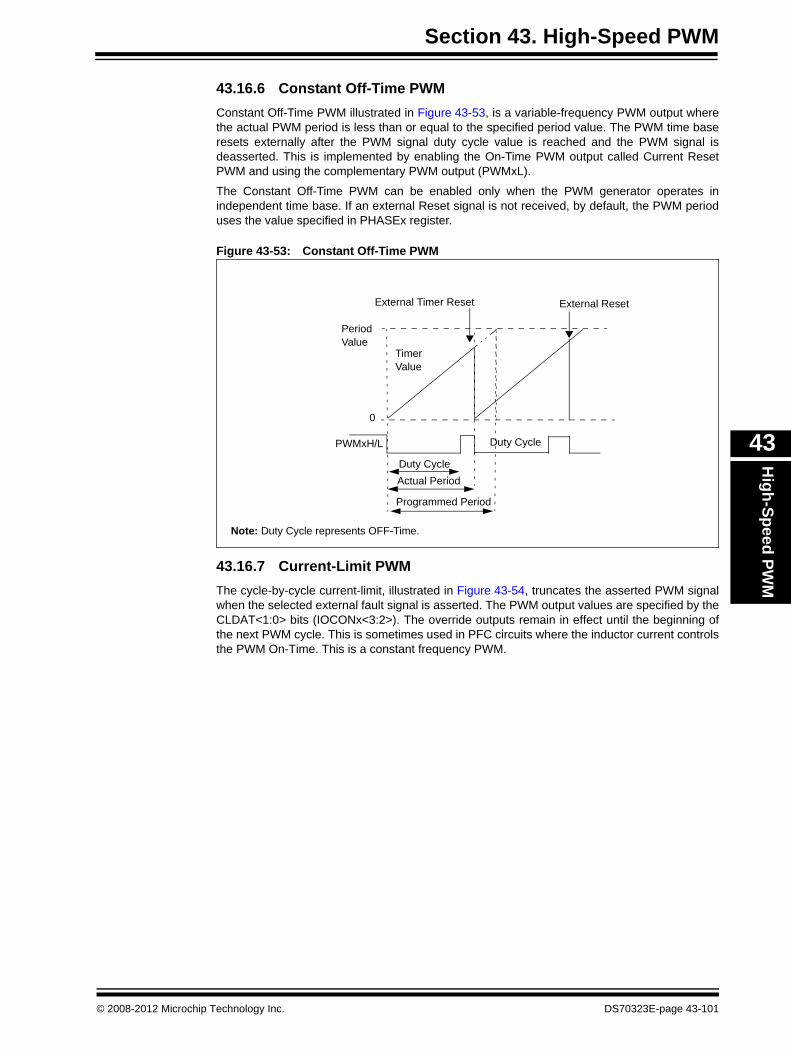
Section 43. High-Speed PWMH
igh-Speed PWM
43
43.16.6 Constant Off-Time PWMConstant Off-Time PWM illustrated in Figure 43-53, is a variable-frequency PWM output wherethe actual PWM period is less than or equal to the specified period value. The PWM time baseresets externally after the PWM signal duty cycle value is reached and the PWM signal isdeasserted. This is implemented by enabling the On-Time PWM output called Current ResetPWM and using the complementary PWM output (PWMxL).
The Constant Off-Time PWM can be enabled only when the PWM generator operates inindependent time base. If an external Reset signal is not received, by default, the PWM perioduses the value specified in PHASEx register.
Figure 43-53: Constant Off-Time PWM
43.16.7 Current-Limit PWMThe cycle-by-cycle current-limit, illustrated in Figure 43-54, truncates the asserted PWM signalwhen the selected external fault signal is asserted. The PWM output values are specified by theCLDAT<1:0> bits (IOCONx<3:2>). The override outputs remain in effect until the beginning ofthe next PWM cycle. This is sometimes used in PFC circuits where the inductor current controlsthe PWM On-Time. This is a constant frequency PWM.
Duty Cycle
0
Period
TimerValue
Programmed Period
PWMxH/L
Value
External Timer Reset
Duty Cycle
Actual Period
External Reset
Note: Duty Cycle represents OFF-Time.
© 2008-2012 Microchip Technology Inc. DS70323E-page 43-101

dsPIC33F/PIC24H Family Reference Manual
Figure 43-54: Current-Limit PWM
+
L
IL
PWM
D VOUT
COUT
˜S
PWMxH/L
PWMxH/LNew Duty Cycle
IL
Programmed Duty Cycle
Current-Limit
Duty Cycle
0
Period
PWMxH/L
Value
FLTx Negates PWM
Duty CycleProgrammed
Duty Cycle
Programmed
Duty CyclePWMxH/L
Duty CycleActual Actual
FLTx Negates PWM
Programmed Period
Current-Limit
DS70323E-page 43-102 © 2008-2012 Microchip Technology Inc.

Section 43. High-Speed PWMH
igh-Speed PWM
43
43.17 BURST MODE IMPLEMENTATIONIn applications where the load current drawn from the converter is much smaller than its nominalcurrent/converter operating at no load, the power drawn from the source can be reduced byforcing the converter into Discontinuous mode. This is achieved by deasserting the PWM outputsfor a specific amount of time using the manual override feature.
Typically, the converter PWM output can be turned off over a period of time based on the outputvoltage regulation, which can reduce the no load power requirements significantly.
43.18 PWM INTERCONNECTS WITH OTHER PERIPHERALS (ADC, ANALOG COMPARATOR AND INTERRUPT CONTROLLER)
Most power conversion applications require close synchronization of the PWM module with otherperipherals, such as the High-Speed 10-bit ADC and the High-Speed Analog Comparator. Dueto the critical timing requirements for power conversion applications, this interconnection mustbe accomplished with little or no CPU overhead. The interconnection should also ensure a fastresponse time, often in the order of nanoseconds.
The High-Speed PWM module contains a number of enhancements for direct interconnects withthe High-Speed 10-bit ADC and the High-Speed Analog Comparator modules. This sectiondescribes each of these enhancements and also identifies examples where these enhancementsare beneficial for power conversion applications.
43.18.1 PWM – ADC Interconnect
43.18.1.1 PRECISE TRIGGERING OF ADC
In digital power supplies, the ADC is used for measurement of feedback signals. These feedbacksignals can have complex waveforms or high noise content; therefore, precise triggering of theADC is important.
Incorrect triggering of the ADC could have a major impact on the operation of the powerconverter. As an example, Figure 43-55 illustrates a DC-DC boost converter with the currentsensor located in series with the source pin of the power MOSFET. This configuration eliminatesthe need for a differential amplifier with a high common mode voltage capability, and therefore,provides a low cost sensing solution. The trade-off is that the ADC only sees the MOSFETcurrent.
If the digital control system is configured to measure the peak current, a small delay in triggeringthe ADC will yield a result of 0x0000. This delay may be caused by software overheads or if theADC is busy at the sampling instant.
Figure 43-55: Need for Precise ADC Triggering
X
PWM
IL
IR
X
X
Late sample yields zero data
Desired sample point
Critical Edge
+VINIL
L
PWM
VISENSE
VOUT
COUT
+
IRR
Note: Measuring peak inductor current is very important.
Example Boost Converter
© 2008-2012 Microchip Technology Inc. DS70323E-page 43-103

dsPIC33F/PIC24H Family Reference Manual
The scenario previously described can be prevented by using the flexible ADC triggeringfeatures of the High-Speed PWM module. The Special Event Trigger, primary PWM trigger andsecondary PWM trigger can be used to generate an ADC conversion request with no softwareoverhead. This feature guarantees that the ADC conversion is triggered exactly when needed bythe circuitry. As the trigger is sent from the PWM to the ADC module directly in hardware, thisfeature prevents any triggering delays caused by software.
The exact instant when the trigger is generated is determined by the SEVTCMP register for thespecial event trigger, or the TRIGx and STRIGx registers for the PWM primary and secondarytriggers. For more information on the PWM trigger generation, refer to 43.7 “PWM Triggers”.
The High Speed 10-bit ADC provides multiple S&H circuits to allow simultaneous sampling. Thisfeature overcomes the problem of the ADC being busy at the sampling instant. For configuringthe trigger sources of ADC, refer to Section 44. “High-Speed 10-bit ADC” (DS70321).
43.18.1.2 PWM CURRENT-LIMIT TRIGGERING OF ADC
The example of Figure 43-55 can also be implemented using Peak Current mode control. In thismethod, the PWM is automatically truncated by the Current-Limit feature. While the currentlimiting feature is capable of closely controlling the current, the position of the PWM falling edgecannot be predicted. As a result, the Special Event Trigger, primary PWM and secondary PWMtriggers cannot be used to effectively trigger the ADC conversion.
This problem is mitigated by generating the ADC trigger signal directly using the PWMcurrent-limit source. Using this feature the ADC conversion is triggered at the exact instant as thefalling edge of the PWM pulse. Therefore, the peak current measurement can be made reliablyon every falling edge of the PWM signal.
43.18.2 PWM – Analog Comparator Interconnect
43.18.2.1 COMPARATOR CURRENT-LIMITS AND FAULTS
The Current-Limit and Fault functions can be used to limit any system parameter, includingcurrent, voltage, power or temperature on a PWM cycle-by-cycle basis. The Analog Comparatorprovides a unique way of truncating the PWM output directly in hardware.
The truncation of the PWM pulse is accomplished with no software intervention, and can beprogrammed to respond to a variable threshold. The Analog Comparator can also beprogrammed for inverted polarity selection. For example, the inverted polarity may be useful indetecting an under-voltage condition or the absence of a system load.
The cycle-by-cycle Current-Limit or Fault, in conjunction with the analog comparator can also beused for peak current mode control. Figure 43-35 describes the control scheme for implementingpeak current mode control in a boost converter application.
Some instances require the use of the latched fault modes for protecting the system hardware.The High-Speed PWM module provides the latched fault mode by which the PWM outputs areshut down until the fault has been cleared by software. The Analog Comparator may be used forlatching the PWM outputs OFF when the input to the comparator exceeds the Fault threshold.
A good example for using latched fault mode is for short circuit protection. A short circuit eventmay cause catastrophic damage to a power converter, and therefore, cycle-by-cycle Fault is notpreferred. Instead, the PWM outputs can be latched off indefinitely until the software detects thatthe Fault has been cleared.
For more information on how to configure the Analog Comparator as a Current-limit or Faultsource for the PWM module, refer to 43.10.1 “PWM Fault Generated by the AnalogComparator”.
43.18.2.2 EXTERNAL PERIOD RESET MODE
The External Period Reset mode is similar to the Fault/Current-Limit operation, with the exactopposite effect. Instead of shutting down the PWM output, this mode actually resets the PWMperiod, and therefore restarts the PWM sooner than the programmed period.
An example of using the analog comparator for the external period reset mode is described43.16.5 “Current Reset PWM”.
DS70323E-page 43-104 © 2008-2012 Microchip Technology Inc.
Section 43. High-Speed PWMH
igh-Speed PWM
43
43.18.3 PWM – Interrupt Controller Interconnect
43.18.3.1 PWM INTERRUPTS
PWM Interrupts can be generated based on either a PWM fault, current-limit or trigger event.This feature is useful when certain software needs to be executed every time such an eventoccurs.
For example, the PWM Interrupt service routine may contain the fault handling routine thatshould be executed after the PWM has been turned OFF. Tasks such as data logging, externalcommunication of the fault, or the fault recovery routine can be performed here.
The PWM interrupt may also be used for execution of the control algorithm, or update systemvariables or control references.
43.18.3.2 ADC INTERRUPTS AND STAGGERING OF CPU LOAD
One of the unique advantages of using a digital signal controller for power conversion is theability to control multiple stages using a single controller. When multiple control loops areexecuted on the same device, the execution of each loop must be carefully sequenced to avoidany delays in processing the data from the ADC.
The PWM module provides a trigger divider option that can generate the ADC triggers every fewPWM cycles. In addition to this feature, the generation of the first trigger can be delayed tostagger the control loops in the available CPU time.
Figure 43-56 describes the sequence of control loop executions in a system where two powerconverters are simultaneously controlled by a single dsPIC DSC.
As illustrated in Figure 43-56, the ADC pair interrupts are used for executing control algorithmsfor each power converter stage. Each ADC pair conversion is triggered using the PWM triggers.Each PWM trigger is generated every other PWM cycle by using the TRGDIV<3:0> bits(TRGCONx<15:12>). Generation of the first trigger from PWM2 is delayed by one PWM cycleusing the TGSTRT<5:0> bits (TRGCONx<5:0>). With this configuration, the control loopexecution for each power converter is performed on alternate PWM cycles, thus effectivelyutilizing the CPU bandwidth.
© 2008-2012 Microchip Technology Inc. DS70323E-page 43-105

dsPIC33F/PIC24H Family Reference Manual
Figure 43-56: Staggering of CPU Load
PWM2H PWM2L
PWM1H PWM1L
Execute Second Control Loop
Sample and
Convert AN2 and AN3
(Pair 1)
Idle Loop
Execute First
Control Loop
Sample and
Convert AN0 and AN1
(Pair 0)
Idle Loop
Execute First
Control Loop
Sample and
Convert AN0 and AN1
(Pair 0)
Idle Loop
PWM1 Trigger
Execute Second Control Loop
Sample and
Convert AN2 and AN3
(Pair 1)
Idle Loop
Execute First
Control Loop
Idle Loop Execute
Second Control Loop
Sample and
Convert AN2 and AN3
(Pair 1)
Sample and
Convert AN0 and AN1
(Pair 0)
PWM2 Trigger PWM1 Trigger PWM1 Trigger PWM2 Trigger PWM2 Trigger
DS70323E-page 43-106 © 2008-2012 Microchip Technology Inc.

© 2008-2012 M
icrochip Technology Inc.D
S70323E
-page 43-107
Section 43. High-Speed PW
M
4
T
Bit 3 Bit 2 Bit 1 Bit 0 All Resets
SEVTPS<3:0> 0000
— PCLKDIV<2:0> 0000
FFF8
— — — 0000
0000
— CAM XPRES IUE 0000
CLDAT<1:0> SWAP OSYNC 0000
FLTPOL FLTMOD<1:0> 0000
0000
0000
0000
0000
0000
0000
— — — 0000
TRGSTRT<5:0> 0000
— — — 0000
— — — 0000
— — — 0000
formation on available registers.
High-Speed PWM
43
3.19 REGISTER MAPTable 43-8 and Table 43-9 map the bit functions for the High-Speed PWM control registers.
able 43-8: High-Speed PWM Register Map for Devices with Remappable I/O
File Name Bit 15 Bit 14 Bit 13 Bit 12 Bit 11 Bit 10 Bit 9 Bit 8 Bit 7 Bit 6 Bit 5 Bit 4
PTCON PTEN — PTSIDL SESTAT SEIEN EIPU SYNCPOL SYNCOEN SYNCEN — SYNCSRC<1:0>
PTCON2 — — — — — — — — — — — —
PTPER PTPER<15:0>
SEVTCMP SEVTCMP<12:0>
MDC MDC<15:0>
PWMCONx FLTSTAT CLSTAT TRGSTAT FLTIEN CLIEN TRGIEN ITB MDCS DTC<1:0> — —
IOCONx PENH PENL POLH POLL PMOD<1:0> OVRENH OVRENL OVRDAT<1:0> FLTDAT<1:0>
FCLCONx IFLTMOD CLSRC<4:0> CLPOL CLMOD FLTSRC<4:0>
PDCx PDCx<15:0>
PHASEx PHASEx<15:0>
DTRx — — DTRx<13:0>
ALTDTRx — — ALTDTRx<13:0>
SDCx SDCx<15:0>
SPHASEx SPHASEx<15:0>
TRIGx TRGCMP<12:0>
TRGCONx TRGDIV<3:0> — — — — DTM —
STRIGx STRGCMP<12:0>
PWMCAPx PWMCAPx<12:0>
LEBCONx PHR PHF PLR PLF FLTLEBEN CLLEBEN LEB<6:0>
Legend: x = unknown value on Reset, — = unimplemented, read as ‘0’. Reset values are shown in hexadecimal.Note: Not all bits in these registers are available on all devices. Refer to the “High-Speed PWM” chapter in the specific device data sheet for more in

dsPIC33F/PIC
24H Fam
ily Reference M
anual
DS
70323E-page 43-108
© 2008-2012 M
icrochip Technology Inc.
4 Bit 3 Bit 2 Bit 1 Bit 0 All Resets
SEVTPS<3:0> 0000
— PCLKDIV<2:0> 0000
FFF8
— — — 0000
SEVTPS<3:0> 0000
— PCLKDIV<2:0> 0000
FFF8
— — — 0000
— — — 0000
0000
MTBS CAM XPRES IUE 0000
0000
0000
0000
0000
0000
0000
TRGSTRT<5:0> 0000
CLDAT<1:0> SWAP OSYNC 0000
— — — 0000
FLTPOL FLTMOD<1:0> 0000
— — — 0000
L BPHH BPHL BPLH BPLL 0000
— — — 0000
OPSEL<3:0> CHOPHEN CHOPLEN 0000
— — — 0000
ore information on available registers.
Table 43-9: High-Speed PWM Register Map for Devices without Remappable I/O
File Name Bit 15 Bit 14 Bit 13 Bit 12 Bit 11 Bit 10 Bit 9 Bit 8 Bit 7 Bit 6 Bit 5 Bit
PTCON PTEN — PTSIDL SESTAT SEIEN EIPU SYNCPOL SYNCOEN SYNCEN SYNCSRC<2:0>
PTCON2 — — — — — — — — — — — —
PTPER PTPER<15:0>
SEVTCMP SEVTCMP<12:0>
STCON — — — SESTAT SEIEN EIPU SYNCPOL SYNCOEN SYNCEN SYNCSRC<2:0>
STCON2 — — — — — — — — — — — —
STPER STPER<15:0>
SSEVTCMP SSEVTCMP<12:0>
CHOP CHPCLKEN — — — — — CHOP<6:0>
MDC MDC<15:0>
PWMCONx FLTSTAT CLSTAT TRGSTAT FLTIEN CLIEN TRGIEN ITB MDCS DTC<1:0> DTCP —
PDCx PDCx<15:0>
SDCx SDCx<15:0>
PHASEx PHASEx<15:0>
SPHASEx SPHASEx<15:0>
DTRx — — DTRx<13:0>
ALTDTRx — — ALTDTRx<13:0>
TRGCONx TRGDIV<3:0> — — — — DTM —
IOCONx PENH PENL POLH POLL PMOD<1:0> OVRENH OVRENL OVRDAT<1:0> FLTDAT<1:0>
TRIGx TRGCMP<12:0>
FCLCONx IFLTMOD CLSRC<4:0> CLPOL CLMOD FLTSRC<4:0>
STRIGx STRGCMP<12:0>
LEBCONx PHR PHF PLR PLF FLTLEBEN CLLEBEN — — — — BCH BC
LEBDLYx — — — — LEB<8:0>
AUXCONx HRPDIS HRDDIS — — BLANKSEL<3:0> — — CH
PWMCAPx PWMCAPx<12:0>
Legend: x = unknown value on Reset, — = unimplemented, read as ‘0’. Reset values are shown in hexadecimal.Note: Not all bits in these registers are available on all devices. Refer to the “High-Speed PWM” chapter in the specific device data sheet for m

Section 43. High-Speed PWMH
igh-Speed PWM
43
43.20 RELATED APPLICATION NOTESThis section lists application notes that are related to this section of the manual. Theseapplication notes may not be written specifically for the dsPIC33F/PIC24H product family, but theconcepts are pertinent and could be used with modification and possible limitations. The currentapplication notes related to the High-Speed PWM module are:
Title Application Note #No related application notes are available at this time. N/A
Note: Please visit the Microchip web site (www.microchip.com) for additional ApplicationNotes and code examples for the dsPIC33F/PIC24H family of devices.
© 2008-2012 Microchip Technology Inc. DS70323E-page 43-109
dsPIC33F/PIC24H Family Reference Manual
43.21 REVISION HISTORY
Revision A (February 2008)This is the initial released version of the document
Revision B (September 2008)This revision incorporates the following updates:
• Equations:- Updated Equation 43-4 in 43.6 “PWM Generator”- Updated Equation 43-5 in 43.6.2.3 “Secondary Duty Cycle (SDCx)”
• Examples:- Added an example for PWM Clock Code in 43.5.1 “PWM Clock Selection”
• Figures:- Updated the labels in Figure 43-6- Included new figure in 43.6.7 “Dead Time Resolution” (see Figure 43-15)- Updated the fault source values in Figure 43-33 and Figure 43-36
• Headings:- Added Auxiliary PLL as a new section (see 43.5.1 “PWM Clock Selection”)
in 43.5 “Module Description”- The description for Dead Time Distortion has been corrected in 43.6.6 “Dead Time
Distortion”- Added a new section on Dead-Time Insertion in Center-Aligned Mode
(see 43.6.8 “Dead Time Insertion in Center-Aligned Mode”- Added a new sub-section for PWM Fault Generator (see 43.10.1 “PWM Fault
Generated by the Analog Comparator”) in 43.10 “PWM Fault Pins”• Notes:
- Added a note on nominal input clock to the PWM in 43.5.1 “PWM Clock Selection”- Added a note for the boundary conditions of the PWM resolution in the following
registers:• MDC: PWM Master Duty Cycle Register (see Note 2 in Register 43-10)• PDCx: PWM Generator Duty Cycle Register (see Note 2 in Register 43-12)• SDCx: PWM Secondary Duty Cycle Register (see Note 2 in Register 43-13)
- Added a note for using Fault 1 for Current-Limit mode (CLSRC<4:0> = b0000) in Register 43-22 (see Note 2)
- Added a note for configuring the auxiliary clock in 43.5.1 “PWM Clock Selection”- Added a note on resetting the local time base in 43.16.5 “Current Reset PWM”
• Registers:- The register descriptions for the PDCx: PWM Generator Duty Cycle Register and
SDCx: PWM Secondary Duty Cycle Register have been corrected- The bit descriptions for bit 14-10 and bit 7-3 in Register 43-22 have been corrected- Updated the bit field value of LEB as LEB<4:0> and LEB<6:5> in LEBCONx:
Leading-Edge Blanking Control Register (see Register 43-23)- The Read/Write state for the bit 3 through bit 15 have been corrected in PWMCAPx:
Primary PWM Time Base Capture Register (see Register 43-27)• Sections:
- The terms Complementary PWM Output Mode and Complementary PWM Mode have been corrected as Complementary Mode in the entire document
- The terms Push-Pull PWM Output Mode and Push-Pull Mode have been corrected as Push-Pull Mode in the entire document
• Changes to text and formatting were incorporated throughout the document
DS70323E-page 43-110 © 2008-2012 Microchip Technology Inc.

Section 43. High-Speed PWMH
igh-Speed PWM
43
Revision C (March 2010)• Equations:
- Updated the following equations: Equation 43-1, Equation 43-3 through Equation 43-7- Added the following equations: Equation 43-2 and Equation 43-9
• Examples:- Updated the following examples:
• Example 43-1, Example 43-4, Example 43-8, Example 43-11 and Example 43-23• Updated the following changes in Example 43-2: Updated the example and
re-arranged the example to be placed after Example 43-1• Updated the following changes in Example 43-12 and Example 43-13: Updated the
example and re-arranged the example from 43.6.2.4 “Duty Cycle Resolution” to 43.6.2.3 “Secondary Duty Cycle (SDCx)”
- Added the following examples: Example 43-3, Example 43-5, Example 43-14, Example 43-21, Example 43-22 and Example 43-29
• Figures:- Updated the following figures: Figure 43-7, Figure 43-9, Figure 43-10, Figure 43-20
through Figure 43-27, Figure 43-33, Figure 43-36, Figure 43-39 through Figure 43-54- Added the following figures: Figure 43-3, Figure 43-4, Figure 43-8, Figure 43-38,
Figure 43-49 and Figure 43-50• Notes:
- Added a Note with information to customer for utilizing family reference manual sections and data sheets as a joint reference (see note above 43.1 “Introduction”)
- Added Note 2 in Register 43-2 and Register 43-3- Added a Note 1 in Register 43-4- Added Note 5 in Register 43-11- Updated the following changes in Register 43-14:
• Added a sub note in Note 1 and Note 2• Deleted a sub note in Note 2
- Updated the following changes in Register 43-15:• Updated the second sub note in Note 1• Updated the sub note in Note 2
- Updated the bit text description for bit 13-0, in Register 43-16 and Register 43-17- Deleted the note reference for bit 7, and deleted the following note in Register 43-18:
The secondary PWM generator cannot generate PWM trigger interrupts- Added Note 2 in Register 43-19- Added a Note in Register 43-21- Updated Note 1 in Register 43-22- Added a Note 1 in Register 43-23- Added Note 3 and Note 4 in Register 43-27- Updated the following Note in 43.5.1 “PWM Clock Selection”: If the primary PLL is
used as a source for the auxiliary clock, then the primary PLL should be configured up to a maximum operation of FCY = 30 MHz or less, and FVCO must be in the range of 112 MHz - 120 MHz
- Added Note 1 through Note 7 in 43.5.6 “Time Base Synchronization”- Added a Note on duty cycle values in 43.6.7 “Dead Time Resolution”- Added a Note on dynamic triggering in 43.7 “PWM Triggers”- Deleted the following Note in Table 43-3: In the independent time base, the PWMxH
duty cycle is controlled by either MDC or PDCx, and the PWMxL duty cycle is controlled by MDC or SDCx
- Deleted the following Note in Table 43-4: In the Independent output base, the PWMxH duty cycle is controlled by either MDC or PDCx, and the PWMxL duty cycle is controlled by MDC or SDCx
© 2008-2012 Microchip Technology Inc. DS70323E-page 43-111
dsPIC33F/PIC24H Family Reference Manual
Revision C (March 2010) (Continued)- Added a Note on power-saving modes, in 43.14.2 “High-Speed PWM Operation in
Idle Mode”- Updated the Note in 43.16.5 “Current Reset PWM”
• Registers:- Updated the register description for “PWMCAPx: Primary PWM Time Base Capture
Register”, in 43.3 “Control Registers”- Corrected the term “PDCx” as “MDC/PDCx/SDCx” in the bit text ‘0’ description for
bit 0, in Register 43-11- Corrected the term “Data” as “State” in bit 3-2, bit 5-4 and bit 7-6, in Register 43-19- Rearranged Register 43-17: STRIGx: PWM Secondary Trigger Compare Value
Register after Register 43-20 as Register 43-21- Corrected the bit text description for bit 9-3 as “The Blanking can be incremented
in 8.32 ns steps” in Register 43-23• Sections:
- Added “Interleaved Power Factor Correction (IPFC)” in the common applications for the High-Speed PWM, in 43.1 “Introduction”
- Updated the following changes in the list of major High-Speed PWM features, in 43.2 “Features”• Removed “PWM Capture feature”• Updated “Dual trigger from PWM to Analog-to-Digital Converter (ADC) per PWM
period” as “Dual trigger to Analog-to-Digital Converter (ADC) per PWM period”• Updated “Remappable PWMxH and PWMxL Pins” as “Remappable PWM4H and
PWM4L pins”- Updated the following changes in 43.5.1 “PWM Clock Selection”:
• Added the term “Primary PLL Output (FVCO)” in the first paragraph• Corrected the term “PLLCLK” as “FVCO” in the following description: The auxiliary
clock for the PWM module can be derived from the system clock while the device is running in the primary PLL mode. Equation 43-3 gives the relationship between the Primary PLL Clock (FVCO) frequency and the Auxiliary Clock (ACLK) frequency.
- Added 43.5.4.1 “Advantages of Center-Aligned Mode in UPS Applications”.- Updated the following changes in 43.5.6 “Time Base Synchronization”:
• Corrected the pulse width “130 ns” as “200 ns”• Added the following description: The SYNCO signal pulse 200 ns ensures that other
devices reliably sense the signals- Updated the event “When PTEN = 0” as “When PTCON<PTEN> = 0”,
in 43.5.7 “Special Event Trigger”- Deleted the following description in 43.5.8 “Independent PWM Time Base”: The
PHASEx and SPHASEx registers provide the time period value for the PWMx outputs (PWMxH and PWMxL) in Independent Time Base mode
- Updated the following changes in 43.6.3 “Dead Time Generation”:• Added the following description: Dead time is not supported for Independent PWM
Output mode• Removed “(gating)” in the description
- Added the following description in the “Negative Dead Time” sub-section, in 43.6.4 “Dead Time Generators”: Negative dead time is specified only for complementary PWM output signals
- Deleted the following description in 43.6.7 “Dead Time Resolution”: If devices do not implement the High-Resolution PWM option and the PWM clock prescaler resolution is 1.04 ns, 2.08 ns or 4.16 ns, the highest possible dead time resolution is 8.32 ns
- Updated “Dual Trigger Mode bit (DTM<7>) in the TRGCONx register” as “Dual Trigger Mode bit (DTM) in the PWM Trigger Control register (TRGCONx<DTM> = 7)” in 43.7 “PWM Triggers”
DS70323E-page 43-112 © 2008-2012 Microchip Technology Inc.

Section 43. High-Speed PWMH
igh-Speed PWM
43
Revision C (March 2010) (Continued)- Updated the following changes in 43.10.4 “Fault Exit”:
• Removed the following description: The next PWM cycle begins when the PTMR value is zero
• Updated step “c)”- Corrected the term “FSTAT” as “FLTSTAT” in 43.10.5 “Fault Exit with PMTMR
Disabled”- Updated the following changes in 43.10.7 “PWM Current-Limit Pins”:
• Replaced the description “This behavior is called Current Reset mode, which is used in some Power Factor Correction applications” as “Refer to 43.16.5 “Current Reset PWM” for more details”
• Added 43.10.7.2 “Configuring Analog Comparator in Cycle-by-Cycle Mode”.- Updated the following changes in 43.11.1 “Leading-Edge Blanking (LEB)”:
• Updated “8.4 ns” as “8.32 ns”• Added the following description: In High-Speed Switching applications, switches (such
as MOSFETs/IGBTs) typically generate very large transients. These transients can cause problematic measurement errors. The LEB function enables the user-assigned application to ignore the expected transients caused by the transistor switching that occurs near the edges of the PWM output signals.
- Corrected the term “current mode control” as “current-limit PWM control” in 43.11.2 “Individual Time Base Capture”
- Updated the following changes in 43.12.4 “Fault/Current-Limit Override and Dead Time Logic”:• Corrected the following terms in the description: “low” is updated as “inactive” and
“impact” is updated as “aid”• Added the terms “are driven active” in the description
- Added 43.12.6 “PENx (GPIO/PWM) Ownership”- Updated the following changes in 43.15 “External Control of Individual Time
Base(s) (Current Reset Mode)”:• Updated the title “External Control of Individual Time Base(s)” as “External
Control of Individual Time Base(s) (Current Reset Mode)”• Added “Hysteresis and Critical Conduction mode” in the description
- Re-arranged the second paragraph in 43.16.3 “Multi-Phase PWM” as new sub section 43.16.3.1 “Multi-Phase Buck Regulator”
- Added 43.16.3.2 “Interleaved Power Factor Correction (IPFC)”- Added the advantages of Current Reset mode in PFC applications,
in 43.16.5 “Current Reset PWM”- Added 43.17 “Burst Mode Implementation”
• Tables:- Updated the following tables: Table 43-3 and Table 43-4- Added the following tables: Table 43-5 through Table 43-7
• Specific references to “dsPIC33F” are updated as “dsPIC33F/PIC24H” in this Family Reference Manual
• Renamed the Family Reference Manual name “dsPIC33F Section 43. High-Speed PWM” as “dsPIC33F/PIC24H Section 43. High-Speed PWM”
• Changes to text and formatting were incorporated throughout the document
© 2008-2012 Microchip Technology Inc. DS70323E-page 43-113

dsPIC33F/PIC24H Family Reference Manual
Revision D (March 2011) This revision includes the following updates:
• Updated the definitions for the PTCON2, PHASEx, and SPHASEx registers in 43.3 “Control Registers”
• Added Note 2 and Note 3 to the PTCON register (Register 43-1)• Added Note 2 and Note 3 to the shaded note below the SEVTCMP register (Register 43-4)• Removed Note 1 from the STCON register (Register 43-5)• Added Notes 1, 2, and 3 to the SSEVTCMP register (Register 43-8)• Added a new Note 2 to the shaded note below the MDC register (Register 43-10)• Updated Note 1 and added a new Note 3 to the shaded note below the PDCx register
(Register 43-12)• Updated Note 1 and added a new Note 3 to the shaded note below the SDCx register
(Register 43-13)• Updated Note 1 and Note 2 in the shaded note below the PHASEx register
(Register 43-15)• Added a reference to Note 2 to the CLDAT<1:0> bits in the IOCONx register
(Register 43-19)• Updated Note 1 and updated the bit definition for the LEB<6:0> bits in the LEBCONx
register (Register 43-23)• Updated Note 4 in the shaded note in the PWMCAPx register (Register 43-27)• Updated the first sentence of the fourth paragraph in 43.4 “Architecture Overview”• Updated the High-Speed PWM Module Architectural Overview diagram (see Figure 43-1)• Added 120 MHz max to the FVCO reference in the Auxiliary Clock Generation block of the
oscillator system diagram (see Figure 43-3)• Updated the code in Using FVCO as the Auxiliary Clock Source (see Example 43-3)• Updated prescaler option selections in 43.5.2 “Time Base”• Updated the comments and added a line for enabling the independent time base in
Edge-Aligned or Center-Aligned Mode Selection (see Example 43-4)• Updated 43.5.7 “Special Event Trigger”• Updated the code in ADC Special Event Trigger Configuration (see Example 43-7)• Updated 43.5.8 “Independent PWM Time Base”• Updated the second, fourth, and sixth paragraphs and the first bulleted item in
43.6.1 “PWM Period”• Updated the second comment in Clock Prescaler Selection (see Example 43-9)• Added comments to the three lines of code in PWM Time Period Initialization (see
Example 43-11)• Updated the first paragraph in 43.6.2 “PWM Duty Cycle Control”• Updated the first paragraph in 43.6.2.1 “Master Duty Cycle (MDC)”• Updated the first paragraph in 43.6.2.2 “Primary Duty Cycle (PDCx)”• Changed the PWMx signal reference in Primary Duty Cycle Comparison to PWMxH and/or
PWMxL (see Figure 43-12)• Updated the first paragraph in 43.6.2.3 “Secondary Duty Cycle (SDCx)”• Changed the PWMx signal reference in Secondary Duty Cycle Comparison to PWMxL and
updated the note (see Figure 43-13)• Updated the first sentence of the first paragraph in 43.6.2.4 “Duty Cycle Resolution”• Updated the PWM Trigger for Analog-to-Digital Conversion by adding a zero value input to
the DTM multiplexer (see Figure 43-19)• Added the new section 43.18 “PWM Interconnects with Other Peripherals (ADC,
Analog Comparator and Interrupt Controller)”
DS70323E-page 43-114 © 2008-2012 Microchip Technology Inc.

Section 43. High-Speed PWMH
igh-Speed PWM
43
Revision E (July 2012)This revision incorporates the following updates:
• Examples:- Updated 8 MHz to 7.37 MHz, and updated 120 MHz to 117.9 MHz, in Example 43-2
• Equations:- Added Equation title for Equation 43-1 through Equation 43-3- Updated 1.04 ns to 1.06 ns in “The maximum PWM Duty Cycle resolution is 1.04 ns”,
in Equation 43-5• Figures:
- Updated the label FVCO(1) (120 MHz max) to FVCO(1) (80 MHz to 120 MHz max), in Figure 43-3
- Updated Figure 43-8- Updated the label “clk” to “CLK” in Figure 43-12 and Figure 43-13- Updated the font of the decimal numbers to Computer text in the figure title, in
Figure 43-22, Figure 43-25 through Figure 43-27- Updated PTMTMR to PMTMR in Figure 43-28
• Notes:- Updated any references of LSB to LSb in Register 43-8, Register 43-10,
Register 43-12 and Register 43-13- Updated Period - 0x0008 to Period + 0x0008 in Note 1and Note 2, in Register 43-10- Updated Period - 0x0008 to Period + 0x0008 in Note 2 and Note 3, in Register 43-12
and Register 43-13- Updated 1023 ns to 1058 ns in Note 1, in Register 43-23- Updated the following in Register 43-24:
• Removed Note 1, and removed the Note 1 reference in register title• Updated the note references for bit 5 and bit 4
- Updated 1023 ns to 4258 ns in the Note 1, in Register 43-25- Added Note 2 in the note box below Equation 43-1, in 43.5.1 “PWM Clock Selection”- Updated the following in 43.5.6 “Time Base Synchronization”:
• Replaced Note 1: The period of SYNCI pulse should be smaller than the PWM period value to Note 1: The period of SYNCI pulse should be larger than the PWM period value
• Added Note 5- Updated SCDx to SDCx in the Note, in Figure 43-13- Updated - 0x0008 to + 0x0008 in the Note 1 (above Equation 43-5), in
43.6.2.3 “Secondary Duty Cycle (SDCx)”- Added a note in 43.6.8 “Dead Time Insertion in Center-Aligned Mode”- Updated the note in 43.10.1 “PWM Fault Generated by the Analog Comparator”- Added a note in 43.13 “Immediate Update of PWM Duty Cycle”- Added a note in 43.15 “External Control of Individual Time Base(s) (Current Reset
Mode)”• Registers:
- Updated PMTMR to SMTMR in Register 43-7- Updated the bit 15-3 name in Register 43-8- Updated any references of PWMLx and PWMHx to PWMxL and PWMxH in
Register 43-11- Updated the bit value 0 description for bit 0, in Register 43-11- Updated OVDDAT<1:0> bits to OVRDAT<1:0> bits for bit 0, in Register 43-19- Updated 2n * 8.32 ns to 2n * [1/(Auxiliary Clock Frequency)] ns, in Register 43-23
© 2008-2012 Microchip Technology Inc. DS70323E-page 43-115

dsPIC33F/PIC24H Family Reference Manual
Revision E (July 2012) (Continued)• Sections:
- Updated “The SYNCO signal pulse 200 ns ensures that other devices reliably sense the signals” to “The SYNCO signal pulse is 12 TCY clocks wide (about 300 ns at 40 MIPS) to ensure other devices can sense the signal”, in 43.5.6 “Time Base Synchronization”
- Replaced Least Significant Byte (LSB) with LSb in 43.6.2.4 “Duty Cycle Resolution”- Updated the term ‘pin’ to ‘GPIO pin’ in the following sentence: When the port bit for the
pin is set, the fault input will be activated, in 43.10.6 “Fault Pin Software Control”- Updated the following in 43.10.7 “PWM Current-Limit Pins”:
• Updated the first bullet • Updated the term “fault input signal” to “current-limit signal” in the second bullet• Updated the sub bullet “In Independent Fault mode of the IFLTMOD bit, the
CLDAT<1:0> bits are not used for override functions” to “If the Independent Fault Enable bit, IFLTMOD (FCLCONx<15>) is set, the CLDAT<1:0> bits (IOCONx<3:2>) are not used for override functions”
• Updated the sub bullet “In the Current-Limit Mode Enable bit (CLMOD), the current-limit function is enabled. The CLDAT<1:0> bits (High/Low) supply the data values to be assigned to the PWMxH and PWMxL outputs” to “If the IFLTMOD bit (FCLCONx<15>) is clear, and the CLMOD bit (FCLCONx<8>) is set, enabling the current-limit function, then the CLDAT<1:0> bits (High/Low) (IOCONx<3:2>) supply the data values to be assigned to the PWMxH and PWMxL outputs when a current limit is active”
• Tables:- Updated bit 6 to bit 4 for the PWM Clock Prescaler 1:1 in the 16 ns column, in
Table 43-2• Minor updates to text and formatting were incorporated throughout the document
DS70323E-page 43-116 © 2008-2012 Microchip Technology Inc.

Note the following details of the code protection feature on Microchip devices:• Microchip products meet the specification contained in their particular Microchip Data Sheet.
• Microchip believes that its family of products is one of the most secure families of its kind on the market today, when used in the intended manner and under normal conditions.
• There are dishonest and possibly illegal methods used to breach the code protection feature. All of these methods, to our knowledge, require using the Microchip products in a manner outside the operating specifications contained in Microchip’s Data Sheets. Most likely, the person doing so is engaged in theft of intellectual property.
• Microchip is willing to work with the customer who is concerned about the integrity of their code.
• Neither Microchip nor any other semiconductor manufacturer can guarantee the security of their code. Code protection does not mean that we are guaranteeing the product as “unbreakable.”
Code protection is constantly evolving. We at Microchip are committed to continuously improving the code protection features of ourproducts. Attempts to break Microchip’s code protection feature may be a violation of the Digital Millennium Copyright Act. If such actsallow unauthorized access to your software or other copyrighted work, you may have a right to sue for relief under that Act.
Information contained in this publication regarding deviceapplications and the like is provided only for your convenienceand may be superseded by updates. It is your responsibility toensure that your application meets with your specifications.MICROCHIP MAKES NO REPRESENTATIONS ORWARRANTIES OF ANY KIND WHETHER EXPRESS ORIMPLIED, WRITTEN OR ORAL, STATUTORY OROTHERWISE, RELATED TO THE INFORMATION,INCLUDING BUT NOT LIMITED TO ITS CONDITION,QUALITY, PERFORMANCE, MERCHANTABILITY ORFITNESS FOR PURPOSE. Microchip disclaims all liabilityarising from this information and its use. Use of Microchipdevices in life support and/or safety applications is entirely atthe buyer’s risk, and the buyer agrees to defend, indemnify andhold harmless Microchip from any and all damages, claims,suits, or expenses resulting from such use. No licenses areconveyed, implicitly or otherwise, under any Microchipintellectual property rights.
© 2008-2012 Microchip Technology Inc.
QUALITY MANAGEMENT SYSTEM CERTIFIED BY DNV
== ISO/TS 16949 ==
Trademarks
The Microchip name and logo, the Microchip logo, dsPIC, KEELOQ, KEELOQ logo, MPLAB, PIC, PICmicro, PICSTART, PIC32 logo, rfPIC and UNI/O are registered trademarks of Microchip Technology Incorporated in the U.S.A. and other countries.
FilterLab, Hampshire, HI-TECH C, Linear Active Thermistor, MXDEV, MXLAB, SEEVAL and The Embedded Control Solutions Company are registered trademarks of Microchip Technology Incorporated in the U.S.A.
Analog-for-the-Digital Age, Application Maestro, chipKIT, chipKIT logo, CodeGuard, dsPICDEM, dsPICDEM.net, dsPICworks, dsSPEAK, ECAN, ECONOMONITOR, FanSense, HI-TIDE, In-Circuit Serial Programming, ICSP, Mindi, MiWi, MPASM, MPLAB Certified logo, MPLIB, MPLINK, mTouch, Omniscient Code Generation, PICC, PICC-18, PICDEM, PICDEM.net, PICkit, PICtail, REAL ICE, rfLAB, Select Mode, Total Endurance, TSHARC, UniWinDriver, WiperLock and ZENA are trademarks of Microchip Technology Incorporated in the U.S.A. and other countries.
SQTP is a service mark of Microchip Technology Incorporated in the U.S.A.
All other trademarks mentioned herein are property of their respective companies.
© 2008-2012, Microchip Technology Incorporated, Printed in the U.S.A., All Rights Reserved.
Printed on recycled paper.
ISBN: 978-1-62076-441-1
DS70323E-page 43-117
Microchip received ISO/TS-16949:2009 certification for its worldwide headquarters, design and wafer fabrication facilities in Chandler and Tempe, Arizona; Gresham, Oregon and design centers in California and India. The Company’s quality system processes and procedures are for its PIC® MCUs and dsPIC® DSCs, KEELOQ® code hopping devices, Serial EEPROMs, microperipherals, nonvolatile memory and analog products. In addition, Microchip’s quality system for the design and manufacture of development systems is ISO 9001:2000 certified.

DS70323E-page 43-118 © 2008-2012 Microchip Technology Inc.
AMERICASCorporate Office2355 West Chandler Blvd.Chandler, AZ 85224-6199Tel: 480-792-7200 Fax: 480-792-7277Technical Support: http://www.microchip.com/supportWeb Address: www.microchip.comAtlantaDuluth, GA Tel: 678-957-9614 Fax: 678-957-1455BostonWestborough, MA Tel: 774-760-0087 Fax: 774-760-0088ChicagoItasca, IL Tel: 630-285-0071 Fax: 630-285-0075ClevelandIndependence, OH Tel: 216-447-0464 Fax: 216-447-0643DallasAddison, TX Tel: 972-818-7423 Fax: 972-818-2924DetroitFarmington Hills, MI Tel: 248-538-2250Fax: 248-538-2260IndianapolisNoblesville, IN Tel: 317-773-8323Fax: 317-773-5453Los AngelesMission Viejo, CA Tel: 949-462-9523 Fax: 949-462-9608Santa ClaraSanta Clara, CA Tel: 408-961-6444Fax: 408-961-6445TorontoMississauga, Ontario, CanadaTel: 905-673-0699 Fax: 905-673-6509
ASIA/PACIFICAsia Pacific OfficeSuites 3707-14, 37th FloorTower 6, The GatewayHarbour City, KowloonHong KongTel: 852-2401-1200Fax: 852-2401-3431Australia - SydneyTel: 61-2-9868-6733Fax: 61-2-9868-6755China - BeijingTel: 86-10-8569-7000 Fax: 86-10-8528-2104China - ChengduTel: 86-28-8665-5511Fax: 86-28-8665-7889China - ChongqingTel: 86-23-8980-9588Fax: 86-23-8980-9500China - HangzhouTel: 86-571-2819-3187 Fax: 86-571-2819-3189China - Hong Kong SARTel: 852-2401-1200 Fax: 852-2401-3431China - NanjingTel: 86-25-8473-2460Fax: 86-25-8473-2470China - QingdaoTel: 86-532-8502-7355Fax: 86-532-8502-7205China - ShanghaiTel: 86-21-5407-5533 Fax: 86-21-5407-5066China - ShenyangTel: 86-24-2334-2829Fax: 86-24-2334-2393China - ShenzhenTel: 86-755-8203-2660 Fax: 86-755-8203-1760China - WuhanTel: 86-27-5980-5300Fax: 86-27-5980-5118China - XianTel: 86-29-8833-7252Fax: 86-29-8833-7256China - XiamenTel: 86-592-2388138 Fax: 86-592-2388130China - ZhuhaiTel: 86-756-3210040 Fax: 86-756-3210049
ASIA/PACIFICIndia - BangaloreTel: 91-80-3090-4444 Fax: 91-80-3090-4123India - New DelhiTel: 91-11-4160-8631Fax: 91-11-4160-8632India - PuneTel: 91-20-2566-1512Fax: 91-20-2566-1513Japan - OsakaTel: 81-66-152-7160 Fax: 81-66-152-9310Japan - YokohamaTel: 81-45-471- 6166 Fax: 81-45-471-6122Korea - DaeguTel: 82-53-744-4301Fax: 82-53-744-4302Korea - SeoulTel: 82-2-554-7200Fax: 82-2-558-5932 or 82-2-558-5934Malaysia - Kuala LumpurTel: 60-3-6201-9857Fax: 60-3-6201-9859Malaysia - PenangTel: 60-4-227-8870Fax: 60-4-227-4068Philippines - ManilaTel: 63-2-634-9065Fax: 63-2-634-9069SingaporeTel: 65-6334-8870Fax: 65-6334-8850Taiwan - Hsin ChuTel: 886-3-5778-366Fax: 886-3-5770-955Taiwan - KaohsiungTel: 886-7-536-4818Fax: 886-7-330-9305Taiwan - TaipeiTel: 886-2-2500-6610 Fax: 886-2-2508-0102Thailand - BangkokTel: 66-2-694-1351Fax: 66-2-694-1350
EUROPEAustria - WelsTel: 43-7242-2244-39Fax: 43-7242-2244-393Denmark - CopenhagenTel: 45-4450-2828 Fax: 45-4485-2829France - ParisTel: 33-1-69-53-63-20 Fax: 33-1-69-30-90-79Germany - MunichTel: 49-89-627-144-0 Fax: 49-89-627-144-44Italy - Milan Tel: 39-0331-742611 Fax: 39-0331-466781Netherlands - DrunenTel: 31-416-690399 Fax: 31-416-690340Spain - MadridTel: 34-91-708-08-90Fax: 34-91-708-08-91UK - WokinghamTel: 44-118-921-5869Fax: 44-118-921-5820
Worldwide Sales and Service
11/29/11