sebastian hoyos - electrical & computer engineering ...hoyos/courses/689/lecture1.pdfall lecture...
TRANSCRIPT

Spring 2009 S. Hoyos - Advanced Mixed-Signal Interfaces 1
ELEN 689:Special TopicsAdvanced Mixed-Signal Interfaces
Sebastian Hoyos
Texas A&M UniversityAnalog and Mixed Signal Group
Spring 2009 S. Hoyos - Advanced Mixed-Signal Interfaces 2
Administrative
• Instructor: S. Hoyos, 315D WERC, [email protected].
• TA: Srikanth Pentakota #14, 114 WERC .
• Website: www.ee.tamu.edu/~hoyos. All lecture notesand handouts will be posted here.
• Time & Place: TR 3:55 PM to 5:10 PM ENPH 213
• Office Hour: TR 11:00 AM to 12:00PM.
Spring 2009 S. Hoyos - Advanced Mixed-Signal Interfaces 3
Prerequisites
• Signal processing background:– Digital and Statistical Signal Processing
• Analog circuit design background:– Analog Integrated-Circuit Design
• Digital circuit design background:– Basic gate-level logic design knowledge is enough.

Spring 2009 S. Hoyos - Advanced Mixed-Signal Interfaces 4
Course Materials• Textbook: No textbook required.
• References reserved at the Library:
1. IEEE Transactions Journals and Conferences Papers2. Analog MOS Integrated Circuits for Signal Processing, Wiley, 1986
by Gregorian and Temes.
2. Principles of Data Conversion System Design, IEEE Press, 1995by Razavi.
3. CMOS Integrated A/D and D/A Converters, Kluwer, 2003by van de Plassche.
4. Delta-Sigma Data Converters: Theory, Design, and Simulation, Wiley, 1996by Norsworthy, Schreier, and Temes.
5. Analysis and Design of Analog Integrated Circuits, 4th Ed., Wiley, 2001by Gray, Hurst, Lewis, and Meyer.
• Readings: Will be posted on the course website.

Spring 2009 S. Hoyos - Advanced Mixed-Signal Interfaces 5
CAD Tools
• Class accounts.
For questions, contact Manager: Wayne Matous 25 ZEC
• CAD Tools required:
– MATLAB, SimulinkMixed-domain behavioral modeling, analog/digital filter synthesis, and etc.
– Cadence: GUI suite for design entry, layout, waveform display, and etc.• Spectre RF
SPICE-type analyses: .dc, .ac, .xf, .noise, .tran, and etc.Additional capabilities: pss, pac, pxf, pnoise, pdisto to analyze large-signalnonlinear circuits (e.g., switched-capacitor circuits, RF circuits).
• Eldo: For transient noise analysis.
Spring 2009 S. Hoyos - Advanced Mixed-Signal Interfaces 6
Grading
• Homeworks: 15% Biweekly
• Lab: 10%• Project 1: 15%
• Midterm : 20% In class.
• Final Project: 20% Assigned after midterm.
• Proj. Presentation: In class.
• Final Exam: 20% University schedule
Grading Policy: Discussion with classmates is encouraged
but projects that are alike won’t receive credit.

Spring 2009 S. Hoyos - Advanced Mixed-Signal Interfaces 7
Course Outline1. Transmitters (Nyquist rate DACs, Oversampled DACs, Mixers, Filtering)2. Receivers (LNAs, Mixers, Antialiasing Filters, Nyquist rate ADCs, Oversampled ADCs)3. Digitally Assisted Transceivers (Calibration Techniques)4. Applications on Communication Standards (BlueTooth, GSM, EDGE, WIMAX, UWB)5. Software Defined Radios6. Cognitive Radios

Spring 2009 S. Hoyos - Advanced Mixed-Signal Interfaces 8
Methodology• Every lecture will cover a group of papers plus some of the fundamental concepts needed to understand the contributions in the referred papers.
• The papers will be selected from the latest contributions to the state of the art. One of the main goals will be to understand which issues are addressed and why the previous topologies or techniques failed to tackle that issue.
• The students will be encouraged to investigate new and improved techniques.

Spring 2009 S. Hoyos - Advanced Mixed-Signal Interfaces 9
Why Mixed-Signal Interface?
• Nature is analog, not digital.
• Mixed-Signal interface’s role is “translator”.

Spring 2009 S. Hoyos - Advanced Mixed-Signal Interfaces 10
Why CMOS?
Desired features:Low cost Low powerHigh integrationSingle chip radio
TI Bluetooth SoC 2005 ~ 7 mm²
Just 20% of SoC is RF/analog. Rest is digital logic and memory.
Spring 2009 S. Hoyos - Advanced Mixed-Signal Interfaces 11
Digital Signal Processing• Noise immunity, robustness.
• Unlimited precision or accuracy.
• Flexibility, programmability, and scalability.
• Electronic design automation (EDA) tools widely
available and successful.
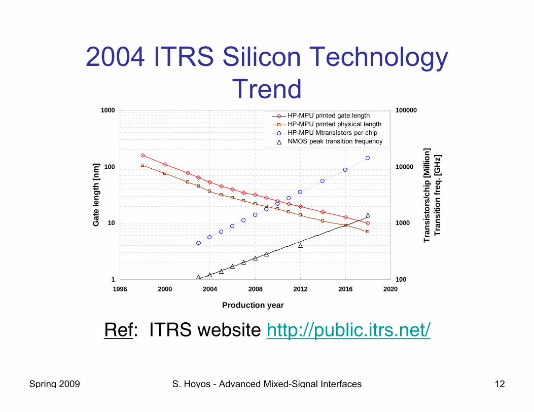
• Benefiting from Moore’s law – “The number of transistors
on a chip doubles every 18 months,” IEDM, 1975.
– Cost/function drops 29% every year.
– That’s 30X in 10 years.
Spring 2009 S. Hoyos - Advanced Mixed-Signal Interfaces 12
2004 ITRS Silicon Technology Trend
Ref: ITRS website http://public.itrs.net/
1
10
100
1000
1996 2000 2004 2008 2012 2016 2020
Production year
Gat
e le
ngth
[nm
]
100
1000
10000
100000
Tran
sist
ors/
chip
[Mill
ion]
Tran
sitio
n fre
q. [G
Hz]
HP-MPU printed gate lengthHP-MPU printed physical lengthHP-MPU Mtransistors per chipNMOS peak transition frequency

Spring 2009 S. Hoyos - Advanced Mixed-Signal Interfaces 13
Analog Signal Processing
• Sensitive to noise – SNR (signal-to-noise ratio).
• Subject to device nonlinearities – THD (total harmonic distortion).
• Sensitive to device mismatch and process variations.
• Difficult to design, simulate, layout, test, and debug.
• Inevitable, often limits the overall system performance.
• Scaling scenario:
– Enjoyed scaling until ~0.35-µm technology node.
– High-speed, low-resolution ADCs keep benefiting.
– High SNR design difficult to scale with low supplies (≤ 3.3V).
Spring 2009 S. Hoyos - Advanced Mixed-Signal Interfaces 14
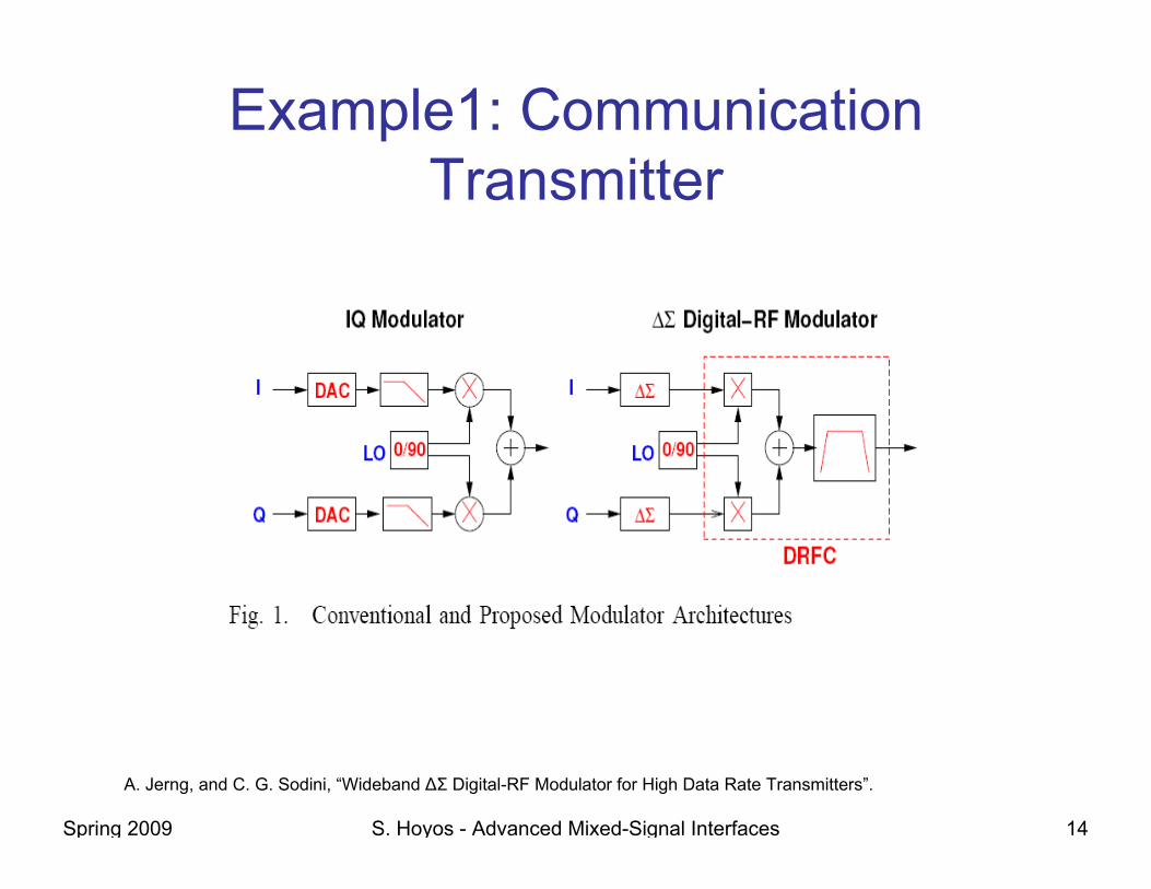
Example1: Communication Transmitter
A. Jerng, and C. G. Sodini, “Wideband ΔΣ Digital-RF Modulator for High Data Rate Transmitters”.
Spring 2009 S. Hoyos - Advanced Mixed-Signal Interfaces 15
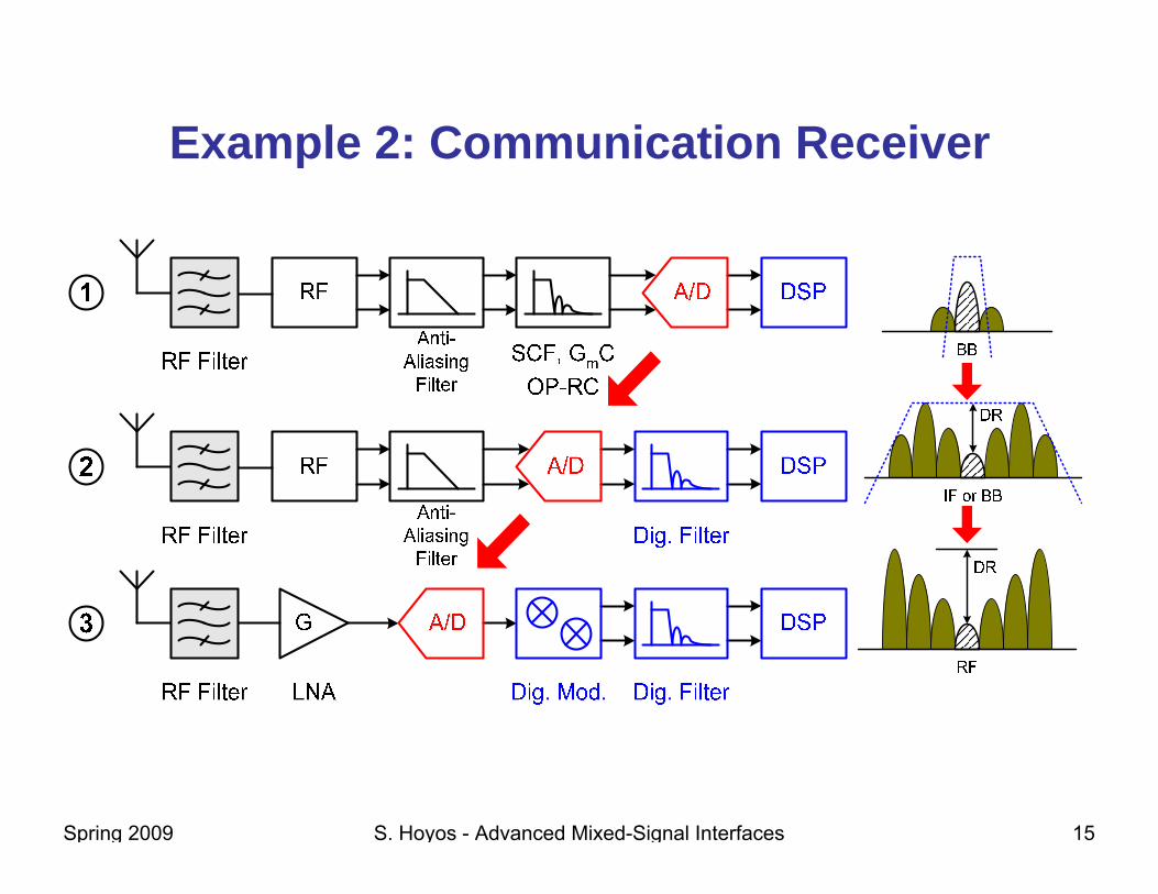
Example 2: Communication Receiver

Spring 2009 S. Hoyos - Advanced Mixed-Signal Interfaces 16
Example 3: Mixed-Signal Hearing Aid
Ref: D. G. Gata, “A 1.1-V 270-μAmixed-signal hearing aid chip,”JSSC, pp. 1670-8, Dec. 2002.
Spring 2009 S. Hoyos - Advanced Mixed-Signal Interfaces 17
ΣΔ Modulator and Transmitter

Spring 2009 S. Hoyos - Advanced Mixed-Signal Interfaces 18
Conventional IQ Modulator
DAC, analog filter and analog mixer. DAC and analog filter more difficult to design as bandwidth and number of bits increase.
Problems: Timing errors, non-linear capacitances, IQ mismatches, DC offsets cause modulator image and LO leakage signals.
Problem: Transmission of spurs outside signal band which are difficult to filter out at RF frequencies. Clock images and quantization noise is upconverted. Need better filtering that just sinc of zero-order-hold.

Spring 2009 S. Hoyos - Advanced Mixed-Signal Interfaces 19
ΣΔ Digital-RF Modulator
Oversampling IQ ΣΔ Modulators.
DRFC is Digital RF converter which combines the functionality of the DAC and mixer.
Spring 2009 S. Hoyos - Advanced Mixed-Signal Interfaces 20
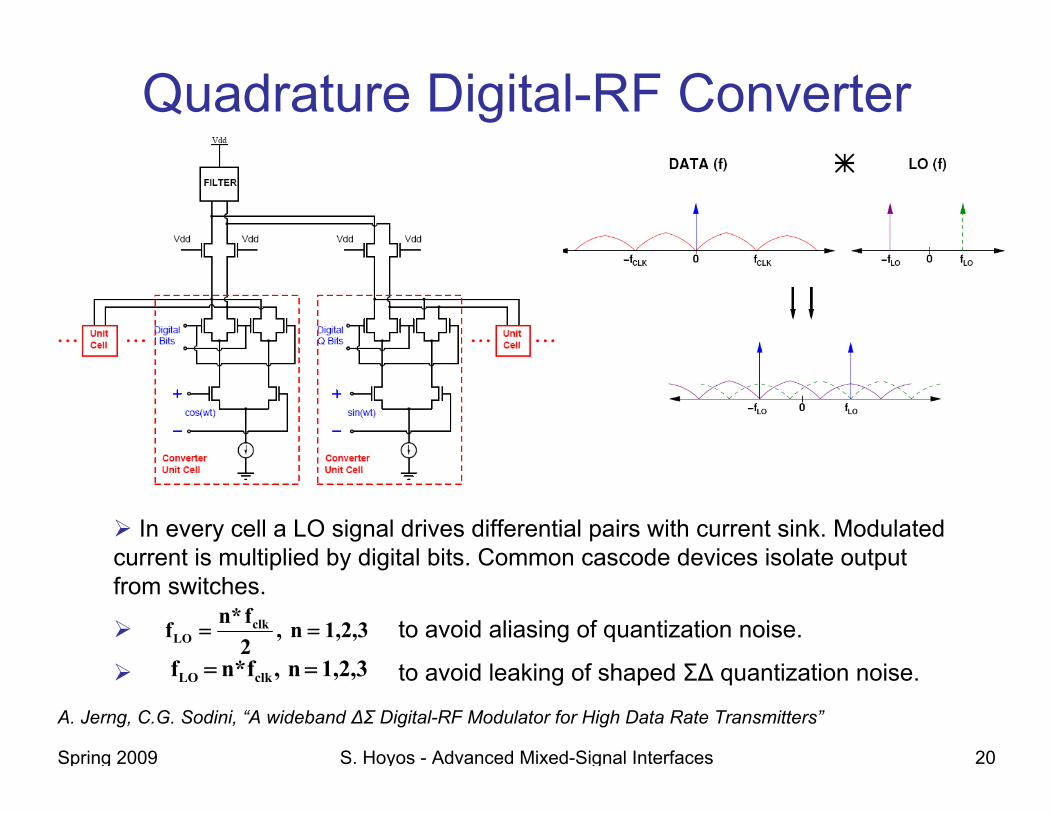
Quadrature Digital-RF Converter
3,2,1,2*
== nfnf clkLO 3,2,1,
2*
== nfnf clkLO
3,2,1,2*
== nfnf clkLO
In every cell a LO signal drives differential pairs with current sink. Modulated current is multiplied by digital bits. Common cascode devices isolate output from switches.
to avoid aliasing of quantization noise.
to avoid leaking of shaped ΣΔ quantization noise.
1,2,3n,2fn*f clk
LO ==
1,2,3n,fn*f clkLO ==
A. Jerng, C.G. Sodini, “A wideband ΔΣ Digital-RF Modulator for High Data Rate Transmitters”

Spring 2009 S. Hoyos - Advanced Mixed-Signal Interfaces 21
Noise Shaping in ΣΔ DACs
( )J(z)1(z)B
ε(z)1(z)B(z)B
ε(z)(z)BJ(z)ε(z)(z)B
inin
out
outin
−−=
+=+
( )J(z)1ε(z) − Noise Transfer Function

Spring 2009 S. Hoyos - Advanced Mixed-Signal Interfaces 22
First Order Noise Shaper
( )1inout z1ε(z)(z)B(z)B −−−=
( )
( ) 211
12tot
21
θ
0s
b1
21212tot
εsinθθ2πθe
cosθ12z1
fπf2θdθz1ε
πθe 1
−=
−=−
=−=
−
−∫1
2θ
0
22uniform θεdθεe 1
== ∫Without Noise Shaping
Dynamic Range Improvement2/1
1
11
tot
uniformtimprovemen θ
sinθ1πθ2
eeDR
−
⎟⎟⎠
⎞⎜⎜⎝
⎛⎟⎟⎠
⎞⎜⎜⎝
⎛−==
Spring 2009 S. Hoyos - Advanced Mixed-Signal Interfaces 23
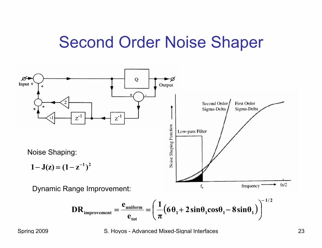
Second Order Noise Shaper
21 )z(1J(z)1 −−=−
Noise Shaping:
( )2/1
1111tot
uniformtimprovemen sinθ8cosθsinθ2θ6
π1
eeDR
−
⎟⎠⎞
⎜⎝⎛ −+==
Dynamic Range Improvement:
Spring 2009 S. Hoyos - Advanced Mixed-Signal Interfaces 24
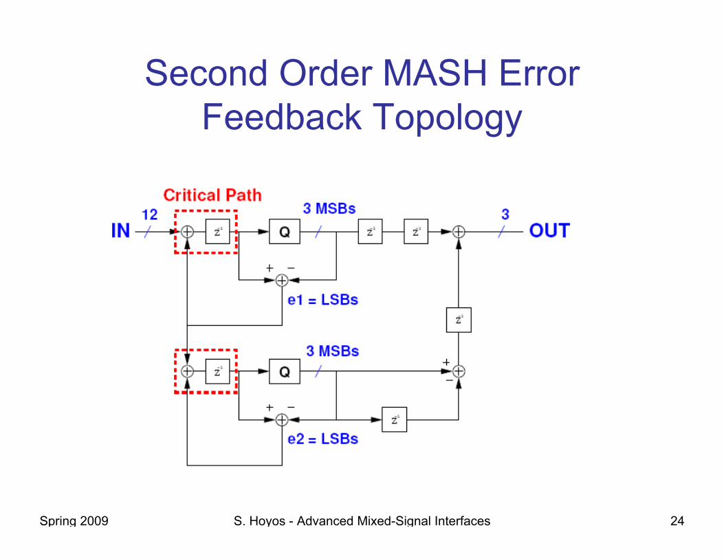
Second Order MASH Error Feedback Topology

Spring 2009 S. Hoyos - Advanced Mixed-Signal Interfaces 25
Third Order Noise Shaper
Case 1: Output Bits larger than 1 Case 2: Just 1 output bit
31 )z(1J(z)1 −−=−Noise Shaping:
Dynamic Range Improvement:
( )2/1
1111.impr θ3sin3/2θ2sin6sinθ30θ20π1DR
−
⎟⎠⎞
⎜⎝⎛ −+−=
Noise Shaping:
3
1
1
az1z1J(z)1 ⎟⎟
⎠
⎞⎜⎜⎝
⎛−−
=− −
−
Spring 2009 S. Hoyos - Advanced Mixed-Signal Interfaces 26
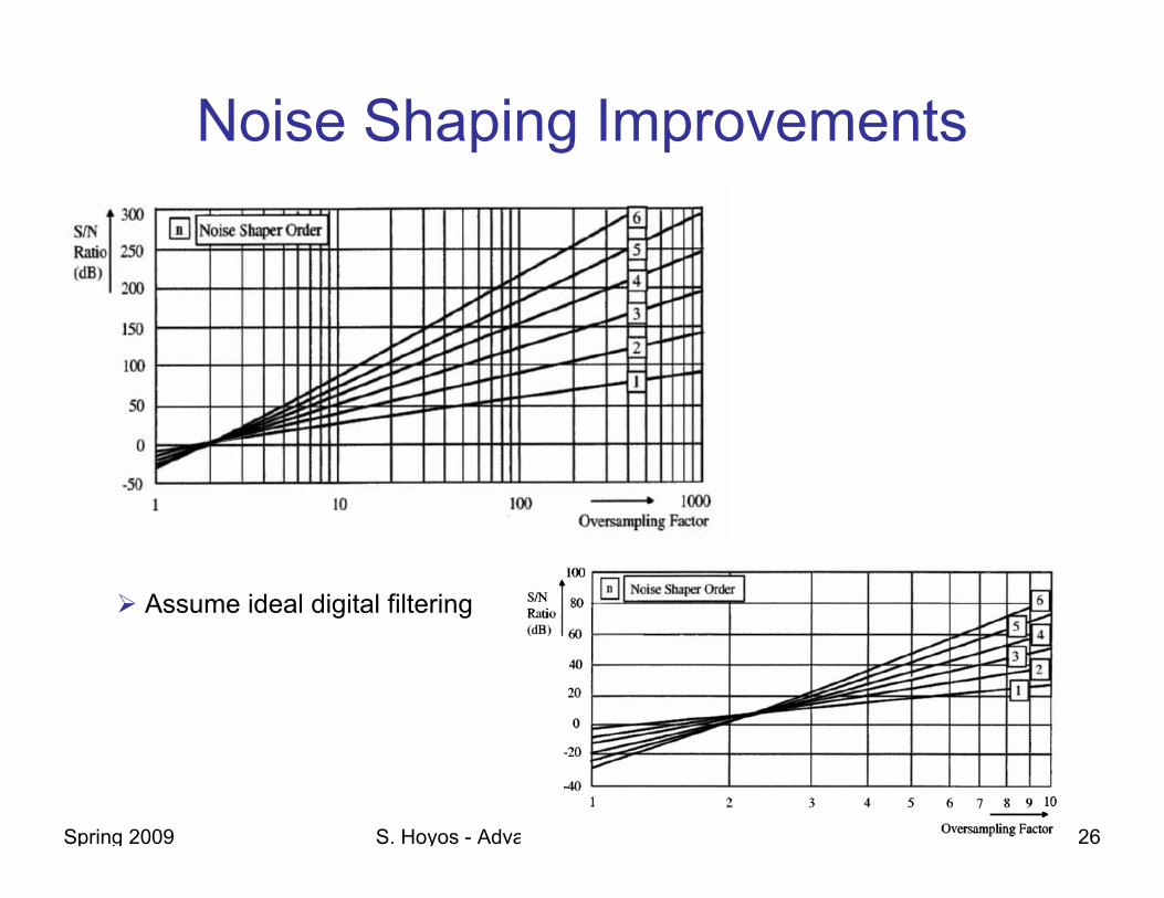
Noise Shaping Improvements
Assume ideal digital filtering

Spring 2009 S. Hoyos - Advanced Mixed-Signal Interfaces 27
Co-Design ΣΔ NTF and BPF
nQOSR
fn*fBW,OSR*f
BW*QfBWfQ
then/LC,1ωandL/R,ωQ
ind
clkLOclk
indLOLO
ind
20ind
≤
==
≤⇒≥
==
indQ ~ 10-25 depending on top metal resistance and distance to substrate.
OSR ~ 10-16, 2nd order and 1 bit SNR=40 dB. Higher order increases the SNR but also increases the slope of the out of band quantization noise which need to be filtered out by the BPF. Low order, multi-bit ΣΔ modulator is a betteroption.
What is the problem with going multi-bit ?

Spring 2009 S. Hoyos - Advanced Mixed-Signal Interfaces 28
Quadrature Digital IFΣΔ modulator can be degraded by spurs coming from LO leakage
and quadrature LO phase mismatches.
A potential solution is digitally up-convert the ΣΔ signal before the RF modulation. LO and image spurs from the digital-RF converter will be separated from the RF output by fIF and 2fIF.
Conventional IF upconversion of fIF=fclk/4 would be convenient because digital cosine and sinesonly have values 1, -1, 0. However there is aliasing of shaped quantization noise from fclk/2.
Quadrature IF upconversion solves the problem.

Spring 2009 S. Hoyos - Advanced Mixed-Signal Interfaces 29
LO phase sensitivity of QuadratureDigital IF
SNR vs. LO Phase Error for Quadrature Digital-IF.
SNR for a 2nd order, 3 bit ΣΔ modulator.

Spring 2009 S. Hoyos - Advanced Mixed-Signal Interfaces 30
Mismatches in the Digital-RF Converter
Small phase mismatches in the LO can be modeled as gain mismatches
The DAC has 3 bits which can be implemented with 7 unit elements cells. Mismatches between the cells will degrade performance as well.
)cos()sin()sin( ttt mismatchesmismatches ωφωφω +=+
Spring 2009 S. Hoyos - Advanced Mixed-Signal Interfaces 31
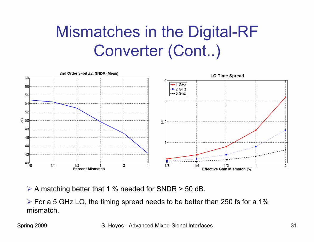
Mismatches in the Digital-RF Converter (Cont..)
A matching better that 1 % needed for SNDR > 50 dB.
For a 5 GHz LO, the timing spread needs to be better than 250 fs for a 1% mismatch.

Spring 2009 S. Hoyos - Advanced Mixed-Signal Interfaces 32
HW 11. Explain why and prove that a discrete signal is periodic with period FCLK.
2. Prove that a real valued signal has an even spectrum. Explain the symmetry differences between discrete-time and continuous-time signals.
3. Prove that multiplication of time domain signals produces convolution of the signals frequency domain. Prove the dual property as well. Explain the differences for this property between discrete-time and continuous-time signals.
4. Derive the noise shaping transfer function of the MASH DAC architecture. Find an expression for the dynamic range improvement vs. OSR. Please provide a plot.

Spring 2009 S. Hoyos - Advanced Mixed-Signal Interfaces 33
Lab 11. Using simulink implement a 2nd order, 3 bit ΣΔ with IF digital modulation.
Consider the following specifications:
fIF= fCLK/4
fLO=fRF± fIF=fRF ± fCLK/4 (use upper-sideband mixing)
fRF=5.25 GHz, fCLK=2.625 GHz, fLO=4.6 GHz.
Simulate the full system and get plots of the spectrum at baseband, IF and RF. Play special attention to the impact of the second harmonic of the LO to the overall noise contribution to the RF signal band. Use a 4th order Bessel filter at 5.25 GHz.
2. Repeat the simulations for the following choice of frequencies: fCLK=2.625 GHz, fIF=600 MHz and fLO=4.65 GHz. Note that fLO is not longer a multiple fCLK, then some aliasing of quantization noise will appear in the RF signal band. The only attenuation is provided by the sinc response of the zero-order-hold.
3. Repeat the simulations for finite rise and fall times (75 ps) of the clock signal. Please derive the new response of the zero-order-hold circuit. Characterize and simulate the improvement of the new filter response. What is the attenuation of the sinc response and the new response at 2fRF?
Spring 2009 S. Hoyos - Advanced Mixed-Signal Interfaces 34
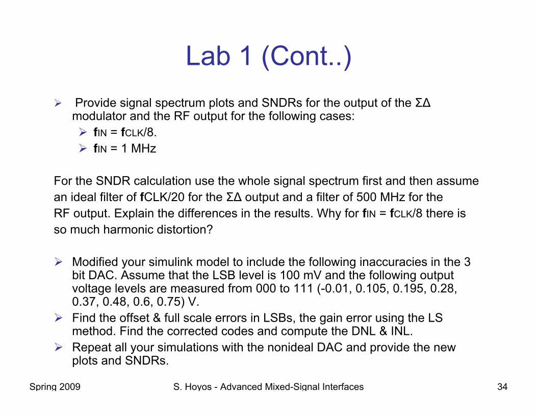
Provide signal spectrum plots and SNDRs for the output of the ΣΔmodulator and the RF output for the following cases:
fIN = fCLK/8. fIN = 1 MHz
For the SNDR calculation use the whole signal spectrum first and then assumean ideal filter of fCLK/20 for the ΣΔ output and a filter of 500 MHz for theRF output. Explain the differences in the results. Why for fIN = fCLK/8 there isso much harmonic distortion?
Modified your simulink model to include the following inaccuracies in the 3 bit DAC. Assume that the LSB level is 100 mV and the following output voltage levels are measured from 000 to 111 (-0.01, 0.105, 0.195, 0.28, 0.37, 0.48, 0.6, 0.75) V.Find the offset & full scale errors in LSBs, the gain error using the LS method. Find the corrected codes and compute the DNL & INL. Repeat all your simulations with the nonideal DAC and provide the new plots and SNDRs.
Lab 1 (Cont..)

Spring 2009 S. Hoyos - Advanced Mixed-Signal Interfaces 35
RF Bandpass Reconstruction Filter
4th order Bessel bandpass filter with 260 MHz of bandwidth at 5.25 GHz.
It a shunt LC resonator. The normalized resonator quality factor
Then,
Tunability with PN junction varactors in the resonator load capacitance.
om
0 QfΔfq =
2.26)297.1(6260925.5q
ΔffQ om ===
ee
Spring 2009 S. Hoyos - Advanced Mixed-Signal Interfaces 36
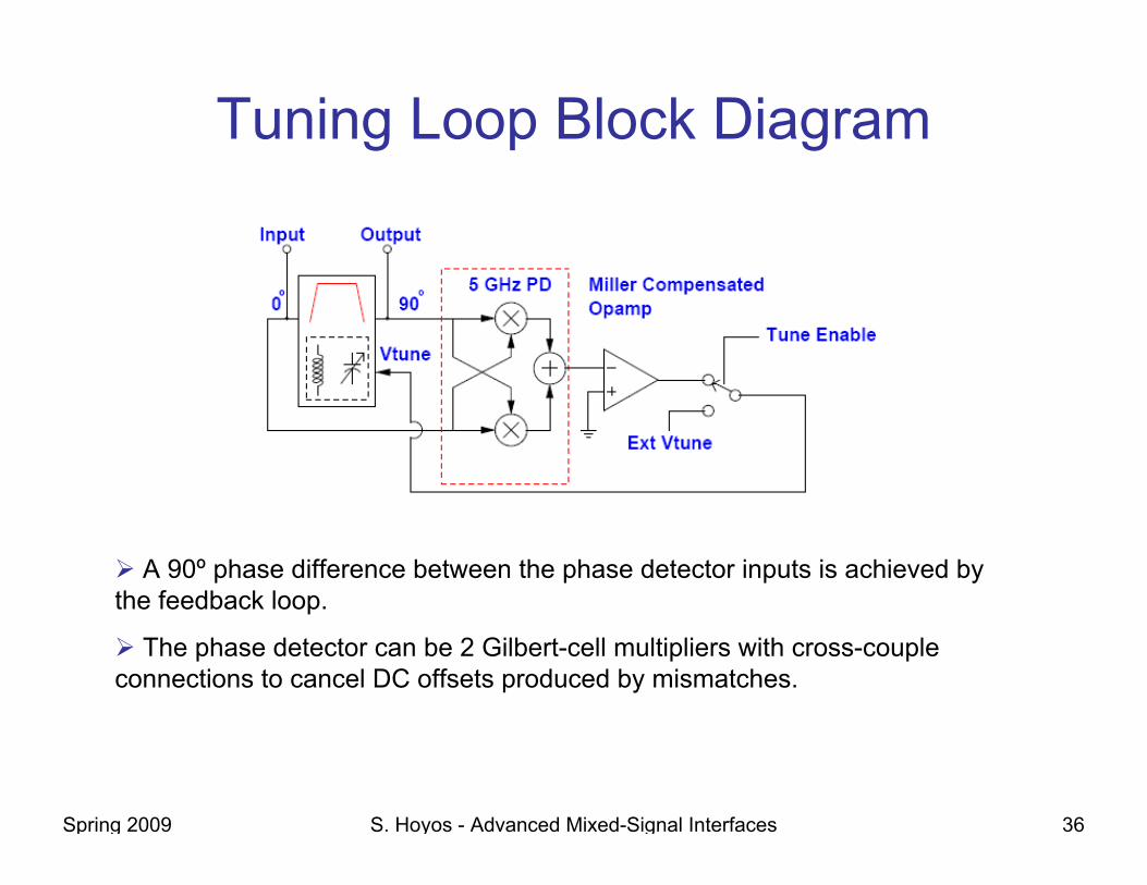
Tuning Loop Block Diagram
A 90º phase difference between the phase detector inputs is achieved by the feedback loop.
The phase detector can be 2 Gilbert-cell multipliers with cross-couple connections to cancel DC offsets produced by mismatches.

Spring 2009 S. Hoyos - Advanced Mixed-Signal Interfaces 37
Distortion vs. TunabilityNonlinearity of the varactor:
......VCVCVCCC(V) 33
2210 ++++=
The I-V relation in the tank:
⎟⎠⎞
⎜⎝⎛ −+=⋅=
ωLj(V)jω
R1VYVI C
Intermodulations: IM3 products produce non-linearity at and .
21 ωω2 −12 ωω2 −
( ) ( )
( )
⎟⎟⎠
⎞⎜⎜⎝
⎛=
−+−++=
⎟⎟⎠
⎞⎜⎜⎝
⎛+++−⋅+=
4RACω310log203(dBc)IM
t)ωωsin(2t)ωωsin(2ACjω43t)sin(ω
RAt)sin(ω
RAI
)Asin(ωt)Asin(ωCjωCjωLωj
R1)Asin(ωt)Asin(ωI
22o
12213
2o21
2212ooo
o21
Only even powers in C(V) matter since it a differential implementation.
Trade-off: higher R, worse IM3 but better Q.

Spring 2009 S. Hoyos - Advanced Mixed-Signal Interfaces 38
Filter Testing Results
Higher C2 also worsens the linearity. The varactor can be operated in amore linear region if fixed switch capacitors are use to increase the tunability. This can lead to a full bank of digitally switchable caps, which requires a digital tuning loop.
⎟⎟⎠
⎞⎜⎜⎝
⎛=
4RACω310log203(dBc)IM
22o

Spring 2009 S. Hoyos - Advanced Mixed-Signal Interfaces 39
DAC Architectures

Spring 2009 S. Hoyos - Advanced Mixed-Signal Interfaces 40
D/A Converter Transfer Characteristic
Note: Vout (bi = 1, for all i) = VFS - Δ = VFS(1-2-N) ≠ VFS
∑∑=
−
=
⋅⋅Δ=⋅=N
i
iNi
N
iii
FSout bbVV11
22
n
Digital input
out
Analog output1
ref
• N = # of bits
• VFS = Full-scale input
• Δ = VFS/2N = 1LSB
• bi = 0 or 1
• Multiplication

Spring 2009 S. Hoyos - Advanced Mixed-Signal Interfaces 41
Ideal DAC Transfer Characteristic
out
000in
001 011 101010 100 110 111
FS
FS
Spring 2009 S. Hoyos - Advanced Mixed-Signal Interfaces 42
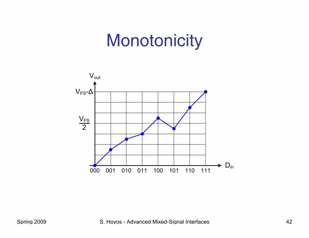
Monotonicity
out
000in
001 011 101010 100 110 111
FS
FS
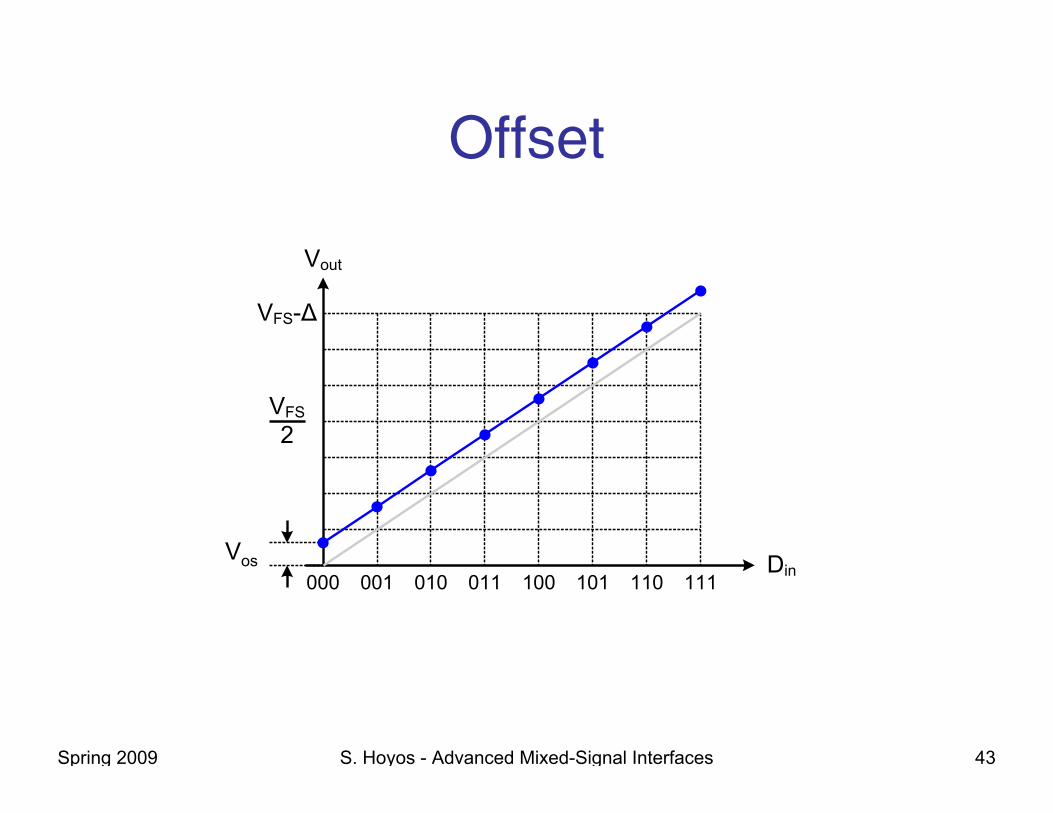
Spring 2009 S. Hoyos - Advanced Mixed-Signal Interfaces 43
Offset
out
000in
001 011 101010 100 110 111
FS
FS
Vos

Spring 2009 S. Hoyos - Advanced Mixed-Signal Interfaces 44
Gain Error
out
000in
001 011 101010 100 110 111
FS
FS
Spring 2009 S. Hoyos - Advanced Mixed-Signal Interfaces 45
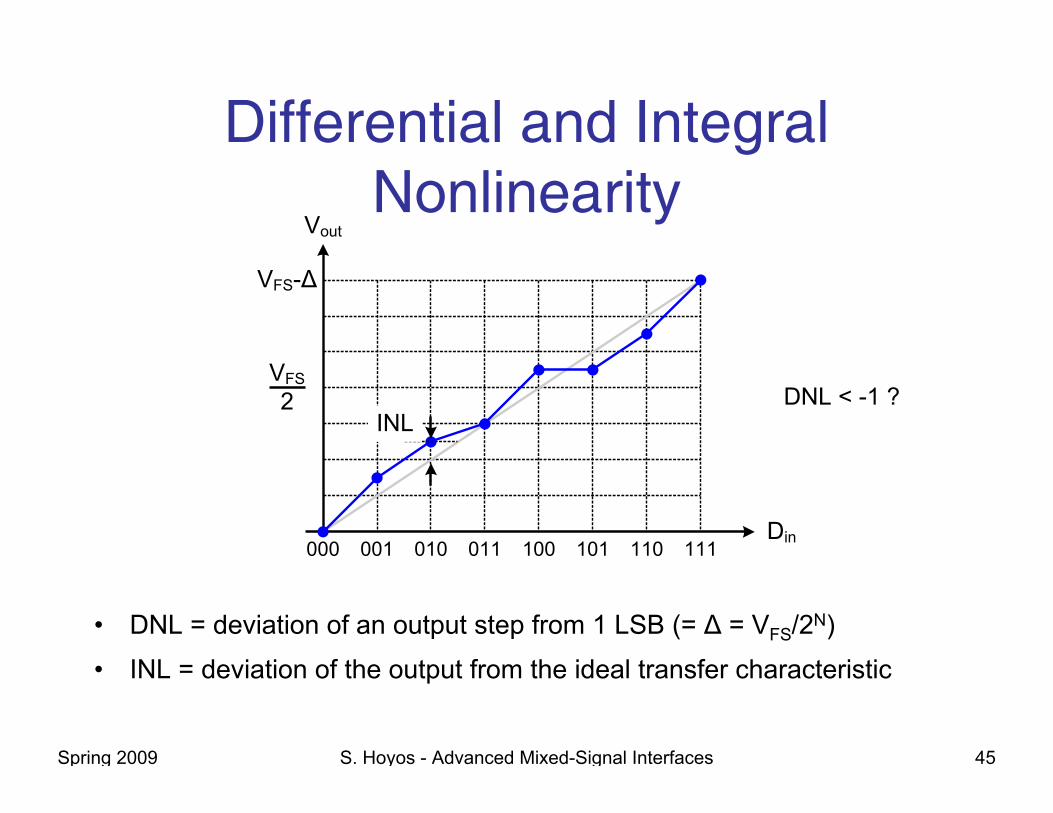
Differential and Integral Nonlinearity
• DNL = deviation of an output step from 1 LSB (= Δ = VFS/2N)
• INL = deviation of the output from the ideal transfer characteristic
DNL < -1 ?
out
000in
001 011 101010 100 110 111
FS
FS
Spring 2009 S. Hoyos - Advanced Mixed-Signal Interfaces 46
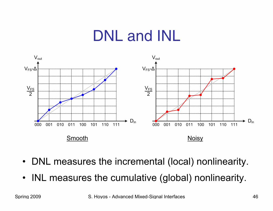
DNL and INL
• DNL measures the incremental (local) nonlinearity.
• INL measures the cumulative (global) nonlinearity.
Vout
000Din
001 011 101010 100 110 111
VFS2
VFS-Δ
Vout
000Din
001 011 101010 100 110 111
VFS2
VFS-Δ
Smooth Noisy
Spring 2009 S. Hoyos - Advanced Mixed-Signal Interfaces 47
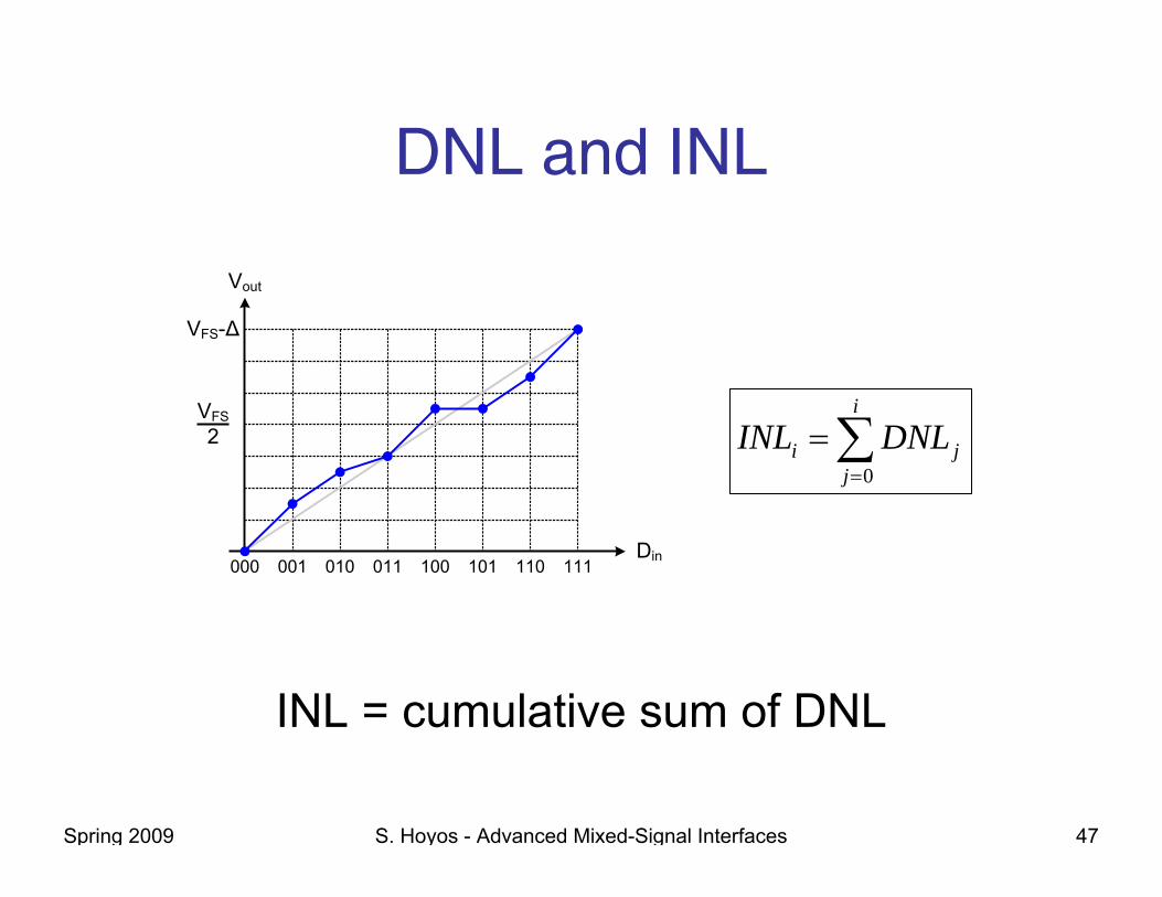
DNL and INL
Vout
000Din
001 011 101010 100 110 111
VFS2
VFS-Δ
∑=
=i
jji DNLINL
0
INL = cumulative sum of DNL
Spring 2009 S. Hoyos - Advanced Mixed-Signal Interfaces 48
out
000in
001 011 101010 100 110 111
FS
FS
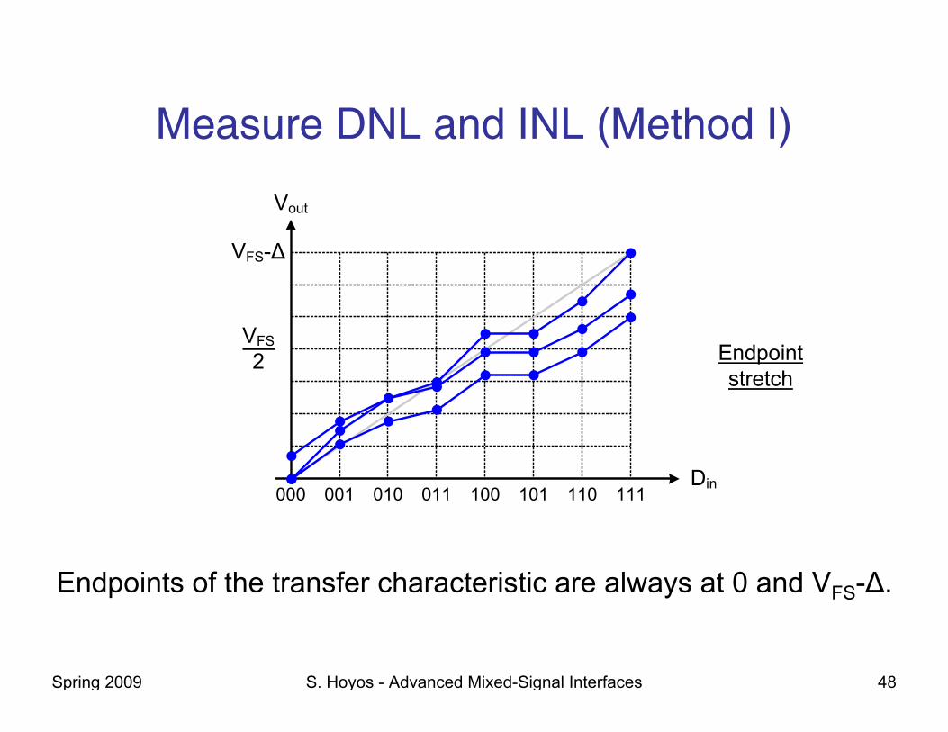
Measure DNL and INL (Method I)
Endpoints of the transfer characteristic are always at 0 and VFS-Δ.
Endpointstretch

Spring 2009 S. Hoyos - Advanced Mixed-Signal Interfaces 49
out
000in
001 011 101010 100 110 111
FS
FS
Measure DNL and INL (Method II)
Least-squarefit and stretch
Endpoints of the transfer characteristic may not be at 0 and VFS-Δ.
Spring 2009 S. Hoyos - Advanced Mixed-Signal Interfaces 50
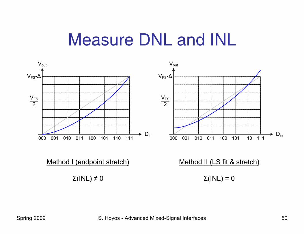
Measure DNL and INL
Method I (endpoint stretch)
Σ(INL) ≠ 0
Method II (LS fit & stretch)
Σ(INL) = 0
Vout
000Din
001 011 101010 100 110 111
VFS2
VFS-Δ
Vout
000Din
001 011 101010 100 110 111
VFS2
VFS-Δ

Spring 2009 S. Hoyos - Advanced Mixed-Signal Interfaces 51
Binary-Weighted DAC

Spring 2009 S. Hoyos - Advanced Mixed-Signal Interfaces 52
Binary-Weighted CR DAC
• Binary-weighted capacitor array → most efficient architecture
• Bottom plate @ VR with bj = 1 and @ GND with bj = 0
Cu = unit capacitanceVX
2Cu Cu Cu8Cu 4Cu
VR
Vo
b3 b2 b1 b0
CP
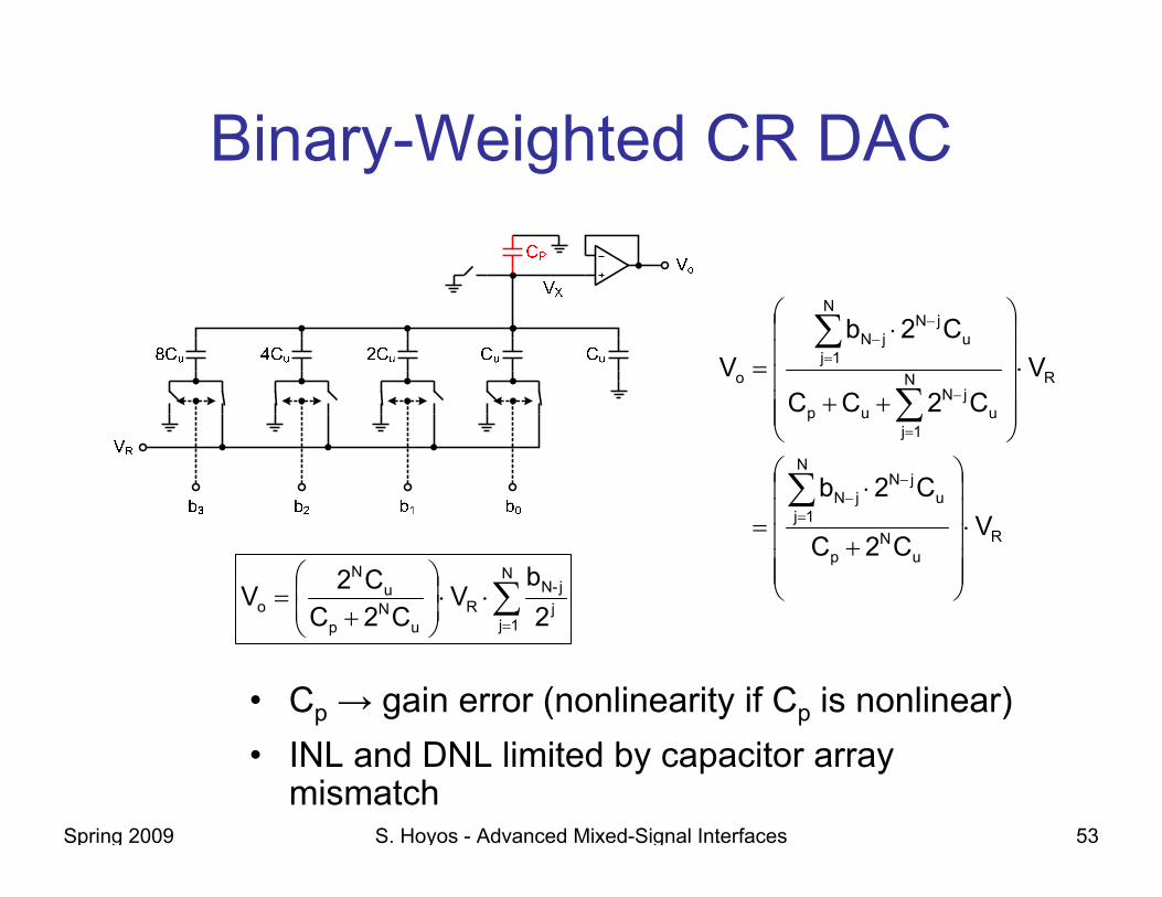
Spring 2009 S. Hoyos - Advanced Mixed-Signal Interfaces 53
Binary-Weighted CR DAC
• Cp → gain error (nonlinearity if Cp is nonlinear)• INL and DNL limited by capacitor array
mismatch
Ru
Np
N
1ju
jNjN
RN
1ju
jNup
N
1ju
jNjN
o
VC2C
C2b
VC2CC
C2bV
⋅
⎟⎟⎟⎟⎟
⎠
⎞
⎜⎜⎜⎜⎜
⎝
⎛
+
⋅=
⋅
⎟⎟⎟⎟⎟
⎠
⎞
⎜⎜⎜⎜⎜
⎝
⎛
++
⋅=
∑
∑
∑
=
−−
=
−
=
−−
∑=
⋅⋅⎟⎟⎠
⎞⎜⎜⎝
⎛
+=
N
1jjj-N
Ru
Np
uN
o 2b
VC2C
C2V

Spring 2009 S. Hoyos - Advanced Mixed-Signal Interfaces 54
Stray-Insensitive CR DAC
∑=
+ ⋅⋅
⎟⎟⎟⎟
⎠
⎞
⎜⎜⎜⎜
⎝
⎛
−++
=N
1jjj-N
Ruu
1Np
uN
uN
o 2b
V
ACC2C
C2
C2V
Large A needed to attenuate summing-node charge sharing

Spring 2009 S. Hoyos - Advanced Mixed-Signal Interfaces 55
MSB Transition
Largest DNL error occurs at the midpoint where MSB transitions, determined by the mismatch between the MSB
capacitor and the rest of the array.
( ) R4
1j
j4p
4o V
C2CC
C1000V ⋅
⎟⎟⎟⎟⎟
⎠
⎞
⎜⎜⎜⎜⎜
⎝
⎛
++=
∑=
−
( ) R4
1j
j4p
321o V
C2CC
CCC0111V ⋅
⎟⎟⎟⎟⎟
⎠
⎞
⎜⎜⎜⎜⎜
⎝
⎛
++
++=
∑=
−
( ) δC,CCCCC :Assume u3214 +=++−
( ) ( )[ ]
uu
oo
CδCC
CC
δC1LSB1LSB0111V1000VDNL
==
−−=
∑∑
Code 0111 Code 1000

Spring 2009 S. Hoyos - Advanced Mixed-Signal Interfaces 56
Midpoint DNL
• δC > 0 results in positive DNL.• δC < 0 results in negative DNL or even
nonmonotonicity.
δC > 0 δC < 0
Spring 2009 S. Hoyos - Advanced Mixed-Signal Interfaces 57
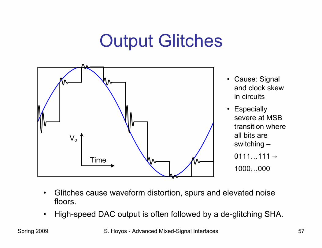
Output Glitches
• Glitches cause waveform distortion, spurs and elevated noise floors.
• High-speed DAC output is often followed by a de-glitching SHA.
• Cause: Signal and clock skew in circuits
• Especially severe at MSB transition where all bits are switching –
0111…111 →1000…000
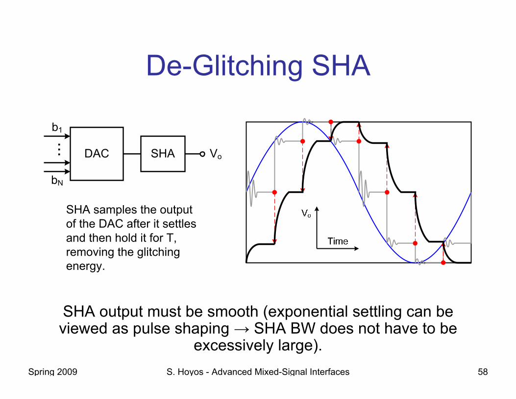
Spring 2009 S. Hoyos - Advanced Mixed-Signal Interfaces 58
De-Glitching SHA
1
N
o
SHA output must be smooth (exponential settling can be viewed as pulse shaping → SHA BW does not have to be
excessively large).
SHA samples the output of the DAC after it settles and then hold it for T, removing the glitchingenergy.
Spring 2009 S. Hoyos - Advanced Mixed-Signal Interfaces 59
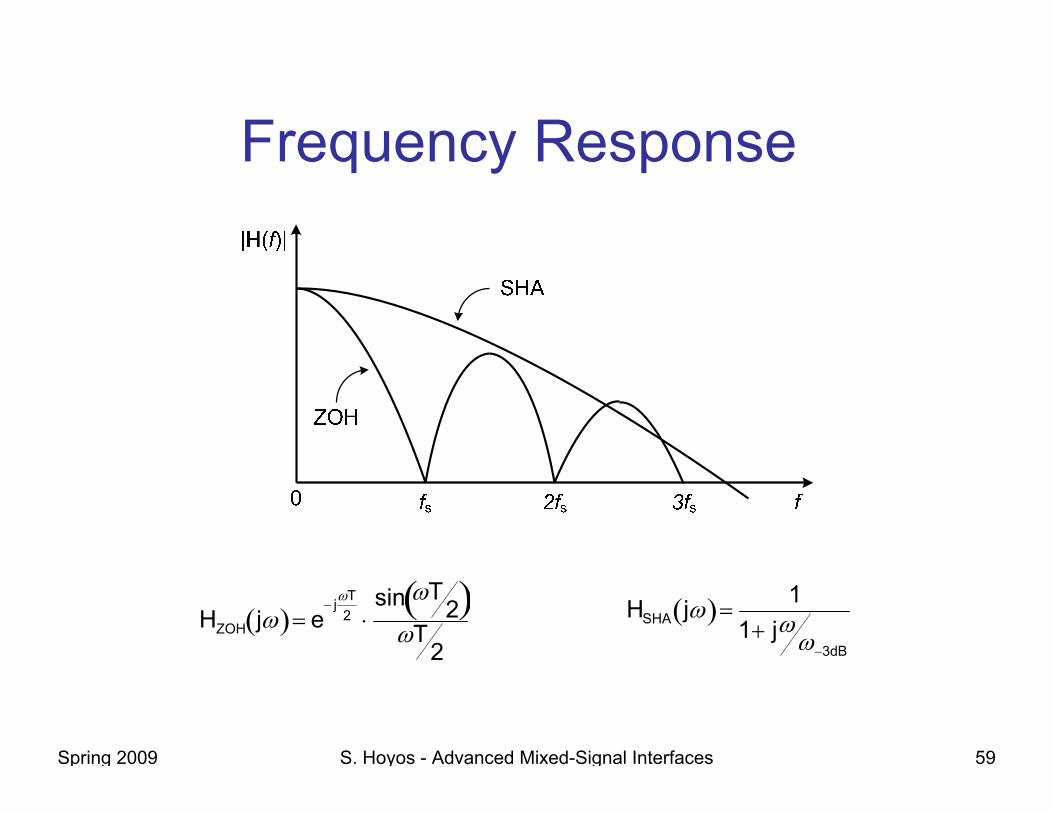
Frequency Response
HZOH jω( )= e
− jωT2 ⋅
sin ωT2( )
ωT2
HSHA jω( )=1
1+ jωω−3dB

Spring 2009 S. Hoyos - Advanced Mixed-Signal Interfaces 60
Binary-Weighted Current DAC
• Current switching is simple and fast.• Vo depends on Rout of current sources without op-amp.• INL and DNL depend on matching, not inherently monotonic.• Large component spread (2N-1:1)
∑=
⋅=N
1jjj-N
o 2b
IRV
Spring 2009 S. Hoyos - Advanced Mixed-Signal Interfaces 61
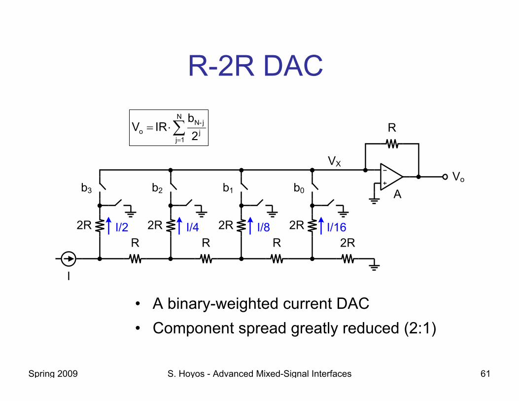
R-2R DAC
• A binary-weighted current DAC• Component spread greatly reduced (2:1)
∑=
⋅=N
1jjj-N
o 2b
IRV
X
o3 2 1 0
Spring 2009 S. Hoyos - Advanced Mixed-Signal Interfaces 62
Unit-Element DAC
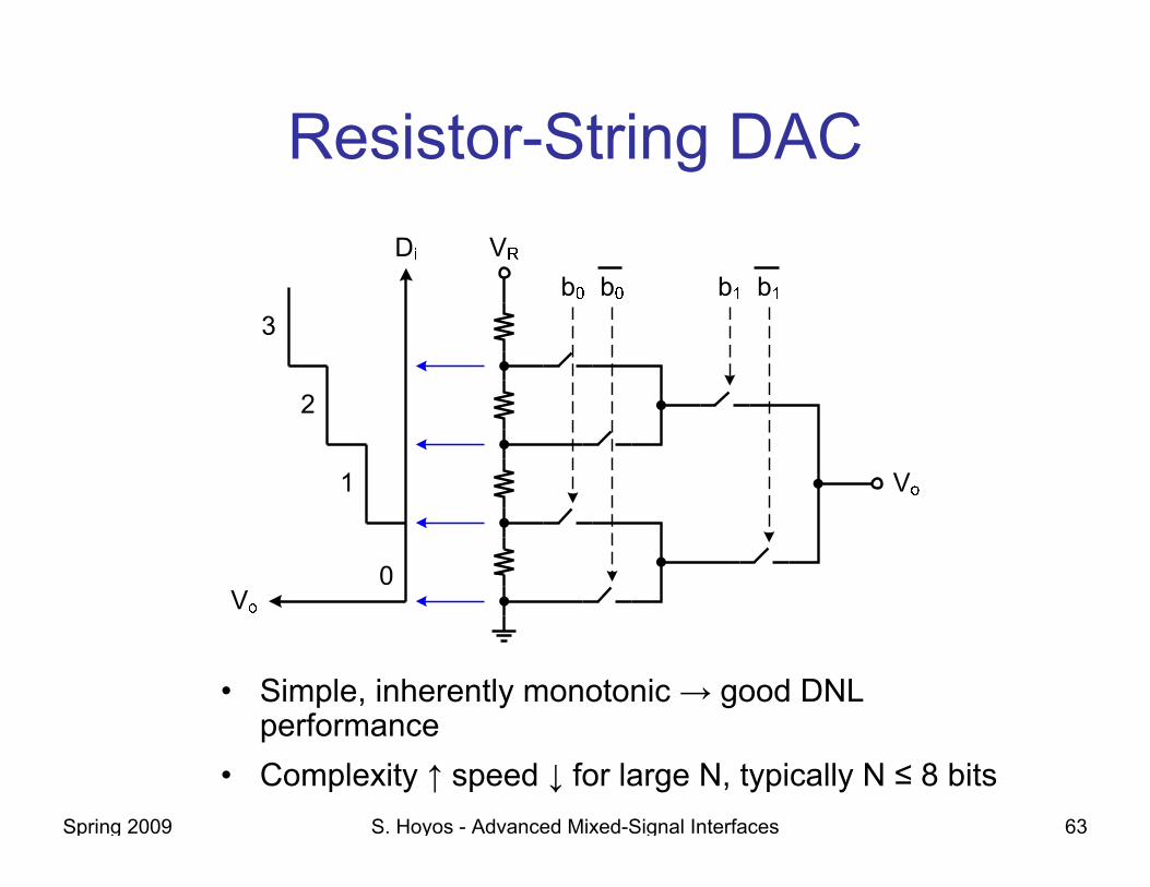
Spring 2009 S. Hoyos - Advanced Mixed-Signal Interfaces 63
Resistor-String DAC
• Simple, inherently monotonic → good DNL performance
• Complexity ↑ speed ↓ for large N, typically N ≤ 8 bits
Spring 2009 S. Hoyos - Advanced Mixed-Signal Interfaces 64
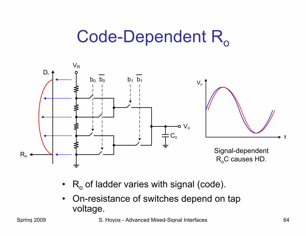
Code-Dependent Ro
• Ro of ladder varies with signal (code).• On-resistance of switches depend on tap
voltage.
VR
Vo
Ro
Dib0 b0 b1 b1
Co
Signal-dependentRoC causes HD.

Spring 2009 S. Hoyos - Advanced Mixed-Signal Interfaces 65
INL and DNL
Vj =Rk
1
j−1
∑
Rk1
N
∑⋅ VR =
j −1( )R + ΔRk1
j−1
∑
NR + ΔRk1
N
∑⋅ VR
Vj-1 =j − 2( )R + ΔRk
1
j−2
∑
NR + ΔRk1
N
∑⋅ VR
Vj − Vj-1 =R + ΔRj−1
NR + ΔRk1
N
∑⋅ VR ≈
VR
N+
ΔRj−1
NR⋅ VR
DNLj = Vj − Vj-1 −VR
N⎛ ⎝ ⎜
⎞ ⎠ ⎟
VR
N≈
ΔRj−1
R⇒ DNL = 0, σDNL =
σR
R.
ΔR = 0,σR[ ]

Spring 2009 S. Hoyos - Advanced Mixed-Signal Interfaces 66
INL and DNL
Vj =Rk
1
j−1
∑
Rk1
N
∑⋅ VR =
j −1( )R + ΔRk1
j−1
∑
NR + ΔRk1
N
∑⋅ VR ≈
j −1N
VR +
N - j +1( ) ΔRk1
j−1
∑ − j −1( ) ΔRkj
N
∑N2R
VR
INLj = Vj −
j -1N
VR⎛ ⎝ ⎜
⎞ ⎠ ⎟
VR
N⇒ INL = 0, σ INL max( ) ≈
N2
σR
R⎛ ⎝ ⎜
⎞ ⎠ ⎟ .
⇒ Vj =j −1N
VR, σ Vj
2 ≈j −1( ) N - j +1( )
N3σR
2
R2 VR2.
⇒ σ Vj
2 max( ) ≈1
4NσR
2
R2 VR2, when j =
N2
+1≈N2
.
Spring 2009 S. Hoyos - Advanced Mixed-Signal Interfaces 67
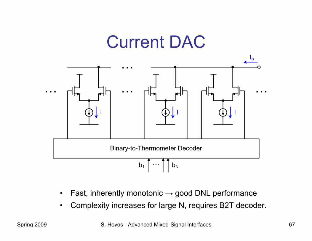
Current DAC
• Fast, inherently monotonic → good DNL performance• Complexity increases for large N, requires B2T decoder.
Io
Binary-to-Thermometer Decoder
b1 bN
I I I

Spring 2009 S. Hoyos - Advanced Mixed-Signal Interfaces 68
Unit Current Cell
• 2N current cells typically broken up into a (2N/2 X 2N/2) matrix
• Current source cascoded to improve accuracy• Coupled inverters improve synchronization of
current switches.
o
1
Nj j

Spring 2009 S. Hoyos - Advanced Mixed-Signal Interfaces 69
Segmented DAC
Spring 2009 S. Hoyos - Advanced Mixed-Signal Interfaces 70
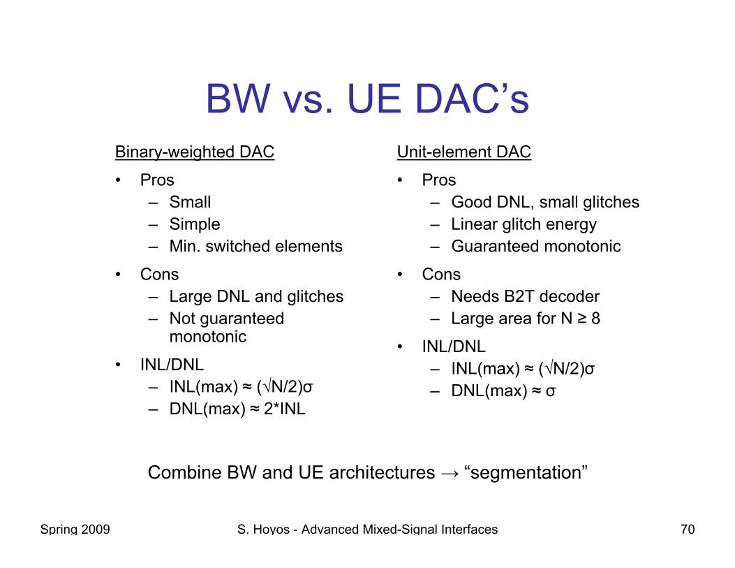
BW vs. UE DAC’sBinary-weighted DAC
• Pros– Small– Simple– Min. switched elements
• Cons– Large DNL and glitches– Not guaranteed
monotonic
• INL/DNL– INL(max) ≈ (√N/2)σ– DNL(max) ≈ 2*INL
Unit-element DAC
• Pros– Good DNL, small glitches– Linear glitch energy– Guaranteed monotonic
• Cons– Needs B2T decoder– Large area for N ≥ 8
• INL/DNL– INL(max) ≈ (√N/2)σ– DNL(max) ≈ σ
Combine BW and UE architectures → “segmentation”
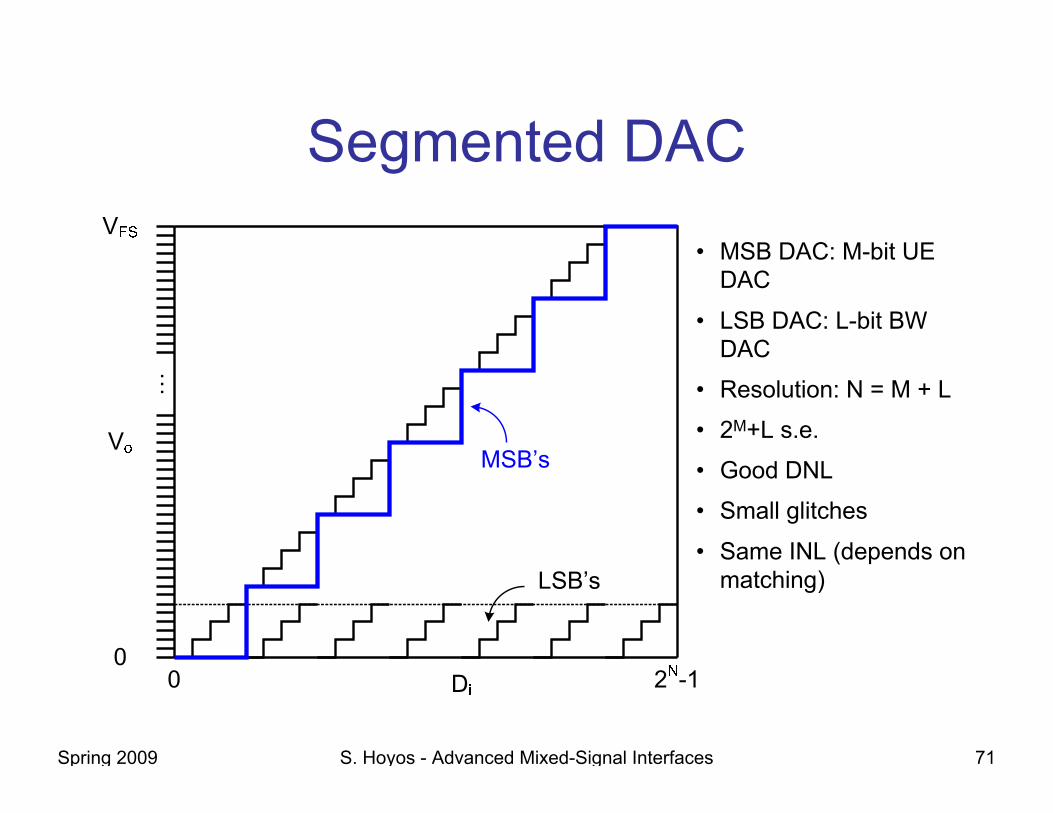
Spring 2009 S. Hoyos - Advanced Mixed-Signal Interfaces 71
Segmented DAC…
• MSB DAC: M-bit UE DAC
• LSB DAC: L-bit BW DAC
• Resolution: N = M + L
• 2M+L s.e.
• Good DNL
• Small glitches
• Same INL (depends on matching)

Spring 2009 S. Hoyos - Advanced Mixed-Signal Interfaces 72
ComparisonExample: N = 12, M = 8, L= 4, σ = 1%
2M+L = 260
0.06 LSB’s
0.32 LSB’sSegmented
N = 120.64 LSB’s
0.32 LSB’s
Binary-weighted
2N = 40960.01 LSB’s
0.32 LSB’sUnit-Element
# of S.E.σDNLσINLArchitecture
Max. DNL error occurs at the MSB segment transitions.
Spring 2009 S. Hoyos - Advanced Mixed-Signal Interfaces 73
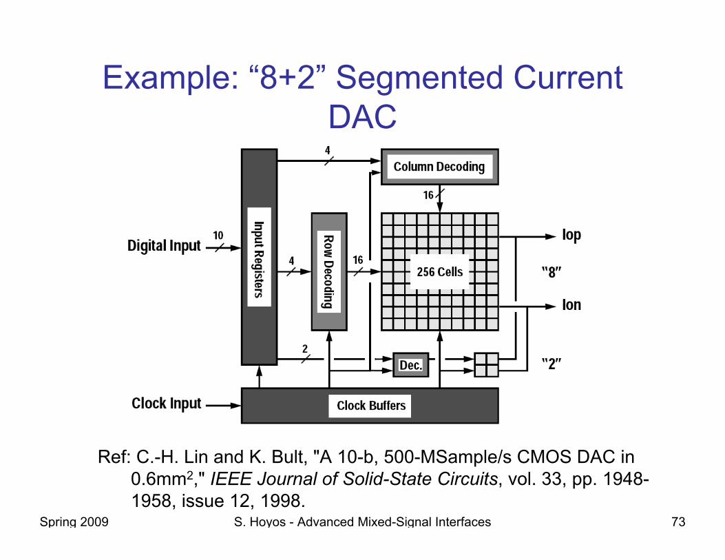
Example: “8+2” Segmented Current DAC
Ref: C.-H. Lin and K. Bult, "A 10-b, 500-MSample/s CMOS DAC in 0.6mm2," IEEE Journal of Solid-State Circuits, vol. 33, pp. 1948-1958, issue 12, 1998.

Spring 2009 S. Hoyos - Advanced Mixed-Signal Interfaces 74
MSB-DAC Biasing Scheme
Common-centroid global biasing + divided 4 quadrants of current cells

Spring 2009 S. Hoyos - Advanced Mixed-Signal Interfaces 75
MSB-DAC Biasing Scheme
Spring 2009 S. Hoyos - Advanced Mixed-Signal Interfaces 76
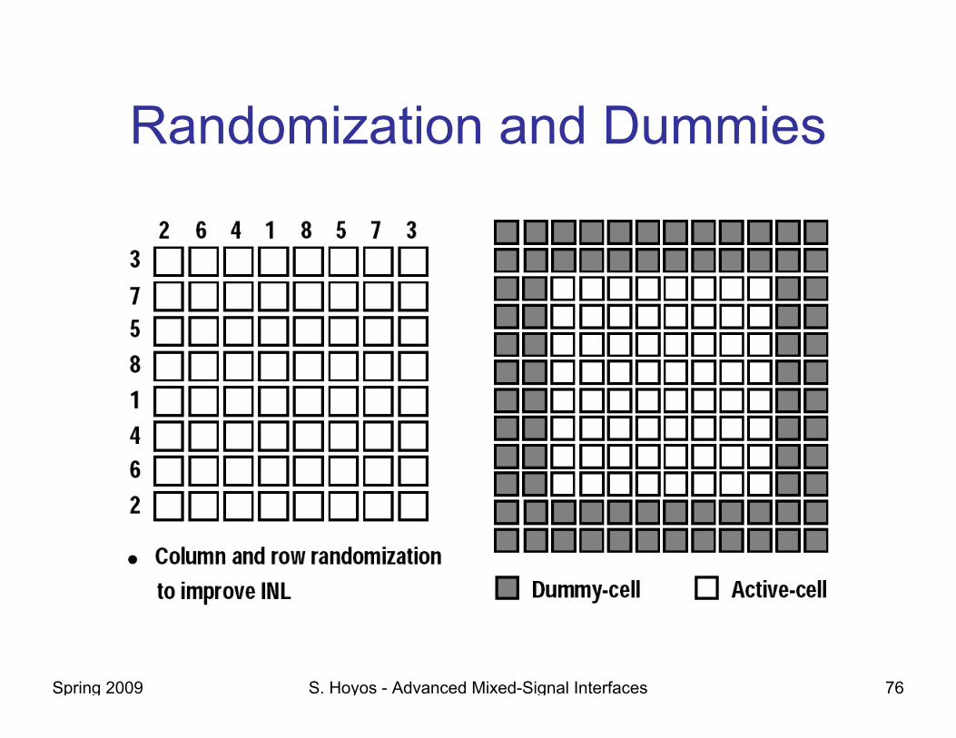
Randomization and Dummies

Spring 2009 S. Hoyos - Advanced Mixed-Signal Interfaces 77
Measured INL and DNL

Spring 2009 S. Hoyos - Advanced Mixed-Signal Interfaces 78
Summary• Nyquist DAC architectures
– Binary-weighted DAC– Unit-element (thermometer-coded) DAC– Segmented DAC– Resistor-string, current, charge-redistribution DAC’s
• Oversampling DAC– Oversampling performed in digital domain (zero stuffing)– Digital noise shaping (ΣΔ modulator)– 1-bit DAC can be used– Analog reconstruction/smoothing filter

Spring 2009 S. Hoyos - Advanced Mixed-Signal Interfaces 79
References1. A. Jerng, C.G. Sodini, “A wideband ΔΣ Digital-RF Modulator for HighData Rate Transmitters”2. Petri Eloranta, et al, “A WCDMA Transmitter in 0.13μm CMOS Using Direct-Digital RF Modulator” ISSCC07.3. R. van de Plassche, “CMOS Integrated A-to-D and D-to-A Converters”4. K. Khanoyan et al., VLSI, 1999, pp. 73-76.5. M. J. M. Pelgrom, JSSC, vol. 25, pp. 1347-1352, issue 6, 1990.6. A. van den Bosch et al., JSSC, vol. 36, pp. 315-324, issue 3, 2001.7. A. R. Bugeja et al., JSSC, vol. 35, pp. 1841-1852, issue 12, 2000.8. G. A. M. Van Der Plas et al., JSSC, vol. 34, pp. 1708-1718, issue 12, 1999.9. A. R. Bugeja et al., JSSC, vol. 34, pp. 1719-1732, issue 12, 1999.10. C.-H. Lin et al., JSSC, vol. 33, pp. 1948-1958, issue 12, 1998.11. K. Falakshahi et al., JSSC, vol. 34, pp. 607-615, issue 5, 1999.12. D. K. Su et al., JSSC, vol. 28, pp. 1224-1233, issue 12, 1993.