school of microelectronic engineering emt362: microelectronic fabrication cmos isolation technology...
TRANSCRIPT
School of Microelectronic Engineering
EMT362: Microelectronic FabricationCMOS ISOLATION TECHNOLOGY
Part 2
Ramzan Mat AyubSchool of Microelectronic Engineering
School of Microelectronic Engineering
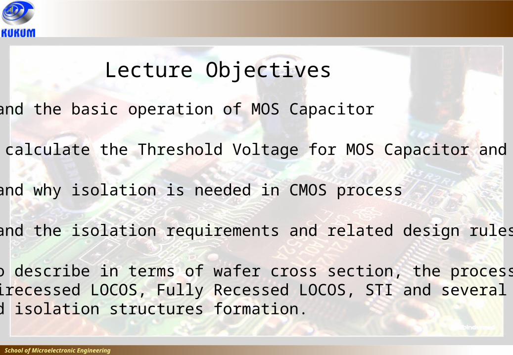
Lecture Objectives
• Understand the basic operation of MOS Capacitor
• Able to calculate the Threshold Voltage for MOS Capacitor and Transistor
• Understand why isolation is needed in CMOS process
• Understand the isolation requirements and related design rules
• Able to describe in terms of wafer cross section, the process steps for Semirecessed LOCOS, Fully Recessed LOCOS, STI and several advanced isolation structures formation.
School of Microelectronic Engineering
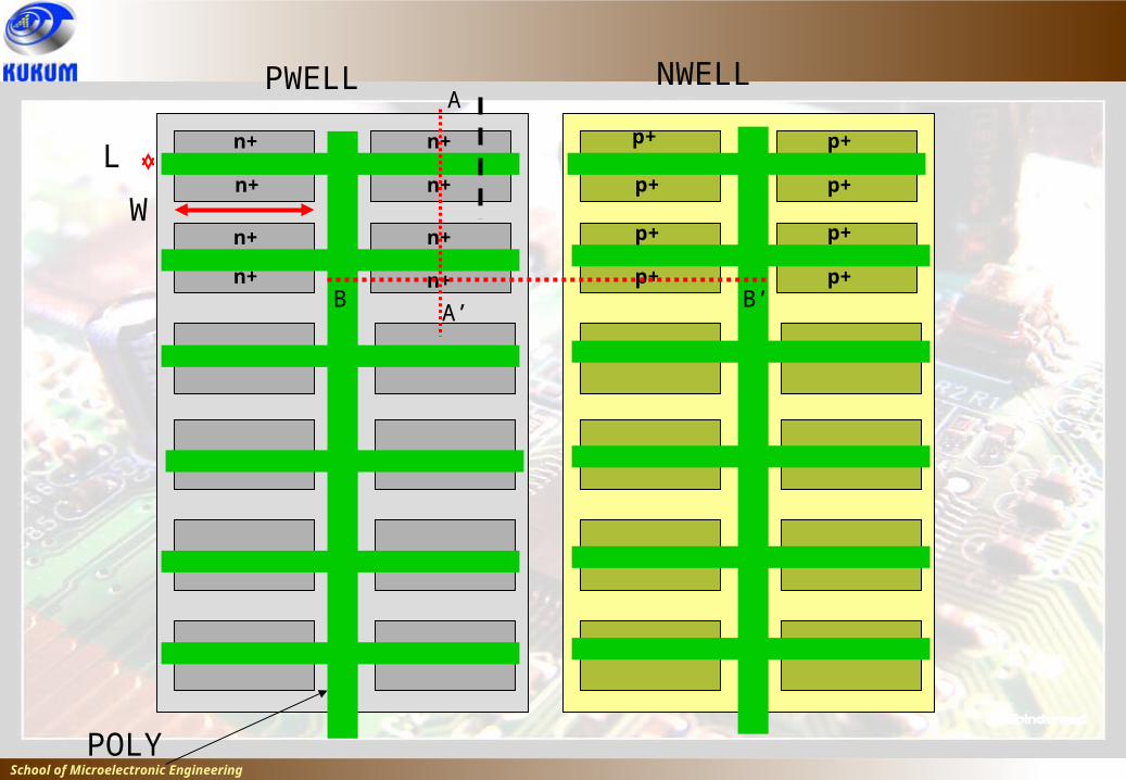
PWELL NWELL
POLY
p+
p+n+
n+ n+
n+
n+
n+
n+
n+L
Wp+p+
p+p+
p+
p+
A
A’B B’
School of Microelectronic Engineering
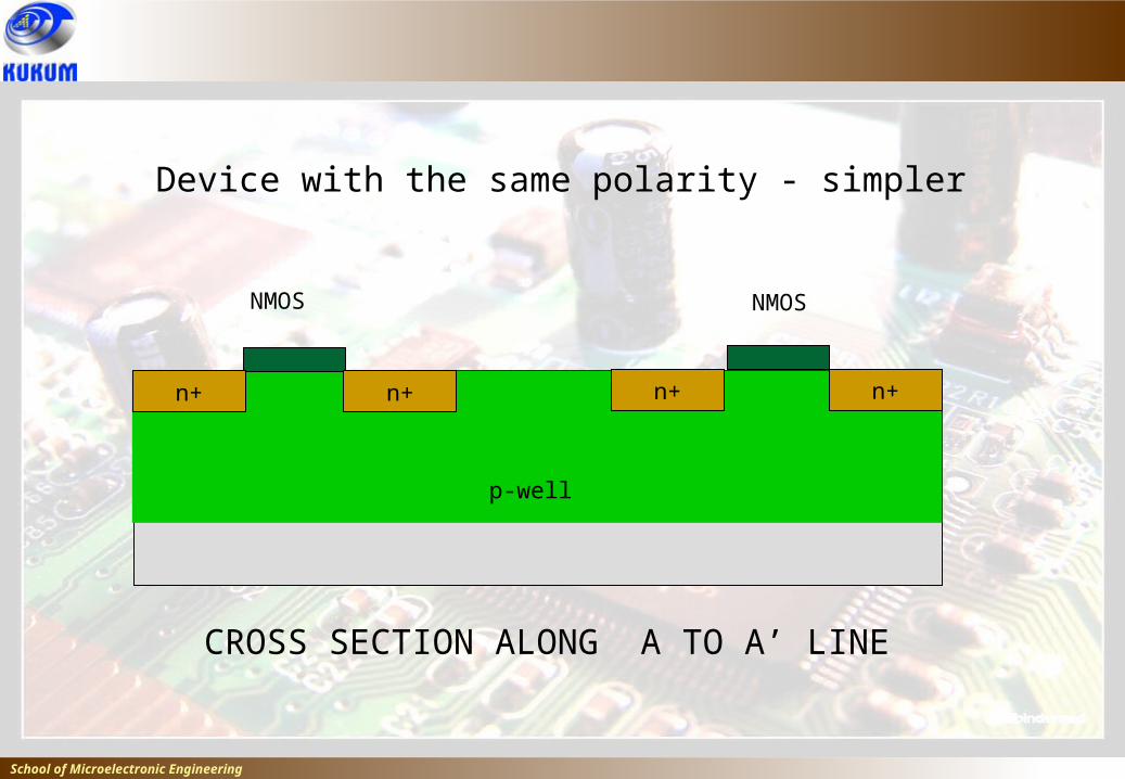
p-well
n+ n+
NMOSNMOS
CROSS SECTION ALONG A TO A’ LINE
n+ n+
Device with the same polarity - simpler
School of Microelectronic Engineering
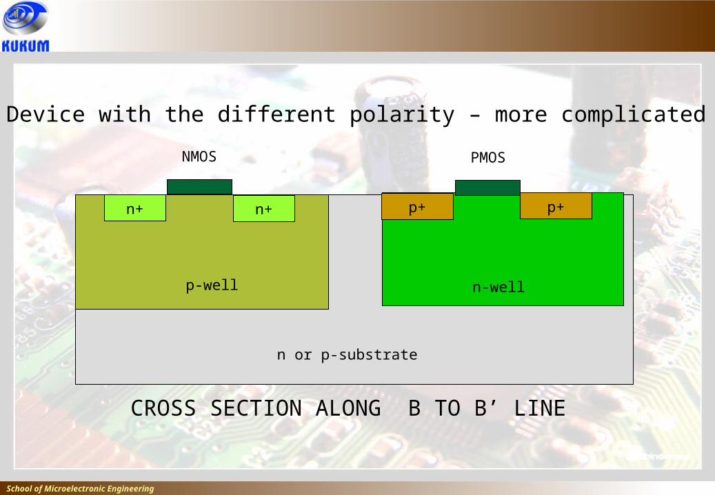
CROSS SECTION ALONG B TO B’ LINE
n or p-substrate
p-well
p+ p+n+n+
PMOSNMOS
n-well
Device with the different polarity – more complicated
School of Microelectronic Engineering
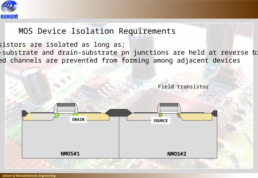
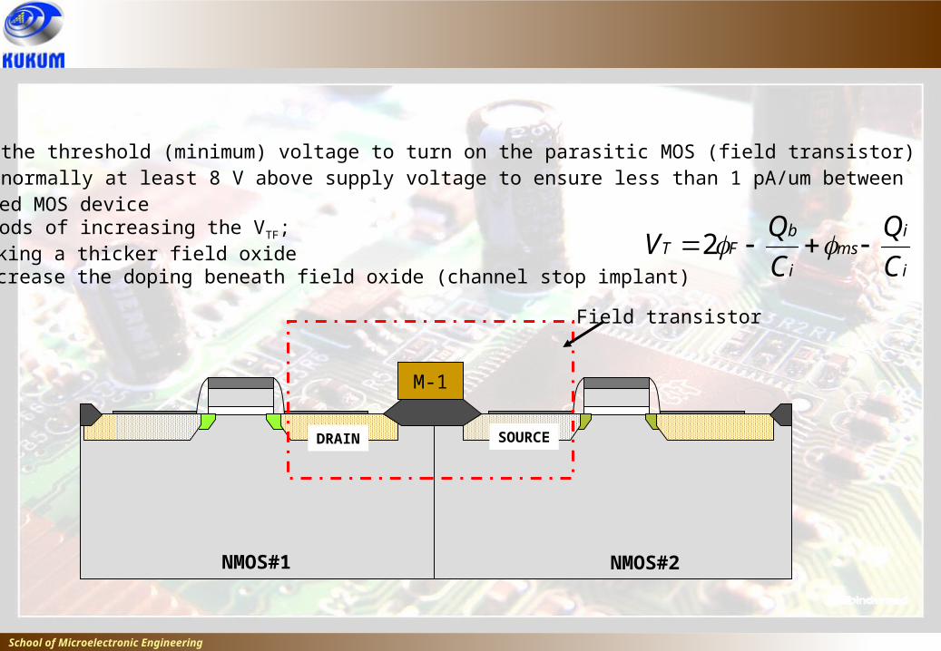
NMOS#2
DRAIN SOURCE
NMOS#1
Field transistor
MOS Device Isolation Requirements
MOS Transistors are isolated as long as;• source-substrate and drain-substrate pn junctions are held at reverse bias• unwanted channels are prevented from forming among adjacent devices
School of Microelectronic Engineering
• Electric circuit in VLSI technology is implemented by connecting isolated devices through specific conducting path. • To fabricate monolithic ICs, electrically isolated devices must be created in the silicon substrate.• Only later they are connected.• Improper isolated device will result;
• total circuit failure• high leakage (large dc power dissipation)• noise margin degradation• voltage shift, cross talk between transistors and etc.
• The challenge is VLSI device only allows single transistor leakage < 10 pA/um). On the other hand, process integration imposed a stringent requirement on the isolation technology;
• spacing between actives should be as small as possible• to produce the surface topography as planar as possible• isolation process module must be simple to implement and easy to control
School of Microelectronic Engineering
School of Microelectronic Engineering
• VTF is the threshold (minimum) voltage to turn on the parasitic MOS (field transistor)• VTF is normally at least 8 V above supply voltage to ensure less than 1 pA/um between
isolated MOS device• 2 methods of increasing the VTF;
• making a thicker field oxide• Increase the doping beneath field oxide (channel stop implant)
NMOS#2
DRAIN SOURCE
NMOS#1
M-1
Field transistor
i
ims
i
bFT
C
Q
C
QV 2
School of Microelectronic Engineering
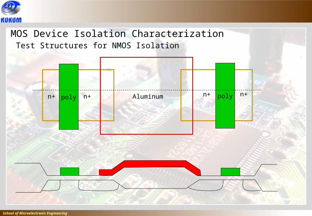
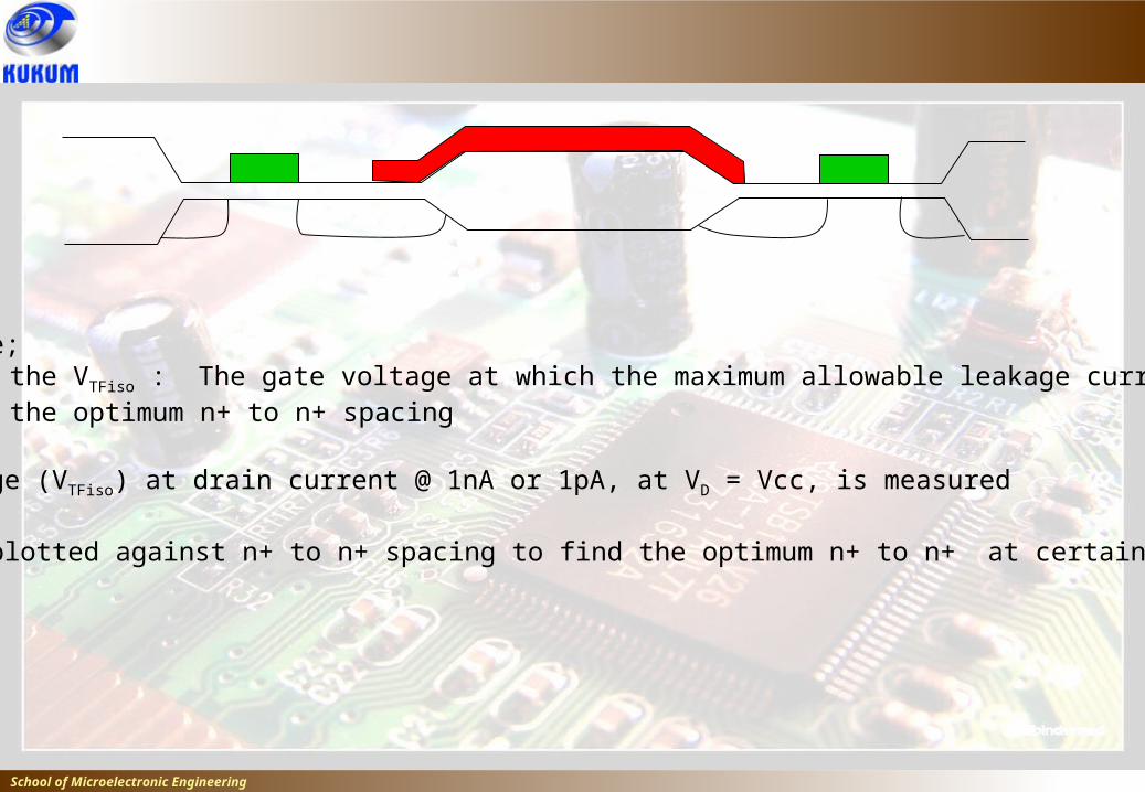
MOS Device Isolation CharacterizationTest Structures for NMOS Isolation
poly polyn+ n+n+ n+ Aluminum
School of Microelectronic Engineering
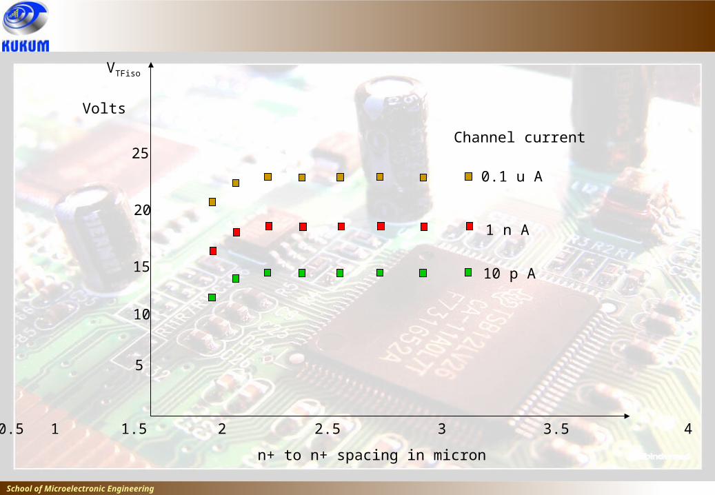
• The purpose;• To find the VTFiso : The gate voltage at which the maximum allowable leakage current arise• To find the optimum n+ to n+ spacing
• Gate voltage (VTFiso) at drain current @ 1nA or 1pA, at VD = Vcc, is measured
• VTFiso is plotted against n+ to n+ spacing to find the optimum n+ to n+ at certain VDS values
School of Microelectronic Engineering
VTFiso
5
10
15
20
25
Volts
0.1 u A
1 n A
10 p A
n+ to n+ spacing in micron
0.5 1 1.5 2 2.5 3 3.5 4
Channel current
School of Microelectronic Engineering
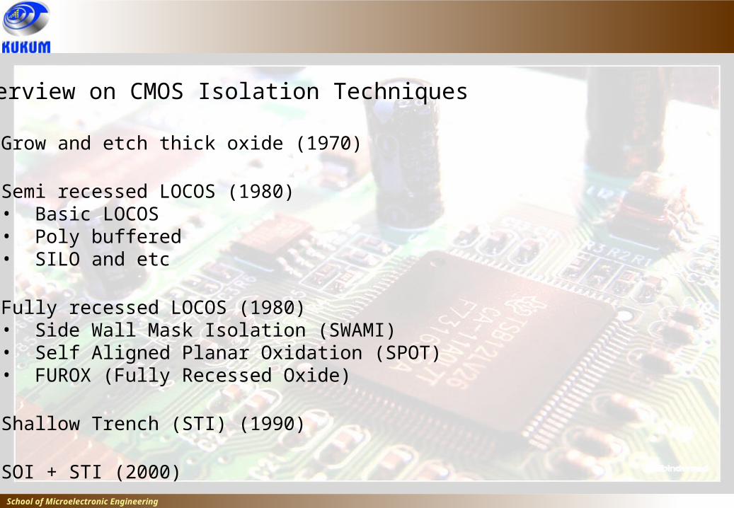
Overview on CMOS Isolation Techniques
• Grow and etch thick oxide (1970)
• Semi recessed LOCOS (1980)• Basic LOCOS• Poly buffered• SILO and etc
• Fully recessed LOCOS (1980)• Side Wall Mask Isolation (SWAMI)• Self Aligned Planar Oxidation (SPOT)• FUROX (Fully Recessed Oxide)
• Shallow Trench (STI) (1990)
• SOI + STI (2000)
School of Microelectronic Engineering
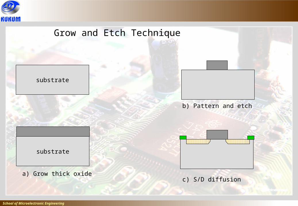
Grow and Etch Technique
substrate
substrate
a) Grow thick oxide
b) Pattern and etch
c) S/D diffusion
School of Microelectronic Engineering
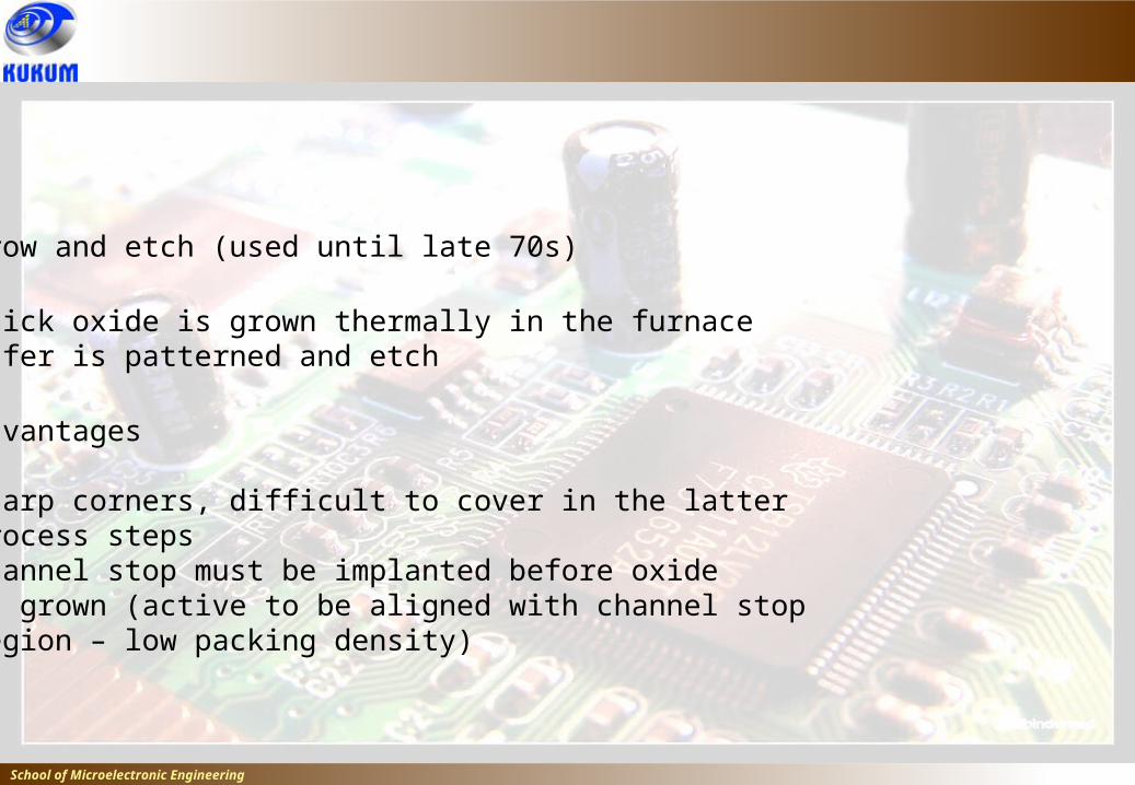
A) Grow and etch (used until late 70s)
• Thick oxide is grown thermally in the furnace• Wafer is patterned and etch
Disadvantages
• Sharp corners, difficult to cover in the latterprocess steps
• Channel stop must be implanted before oxideis grown (active to be aligned with channel stopregion – low packing density)
School of Microelectronic Engineering
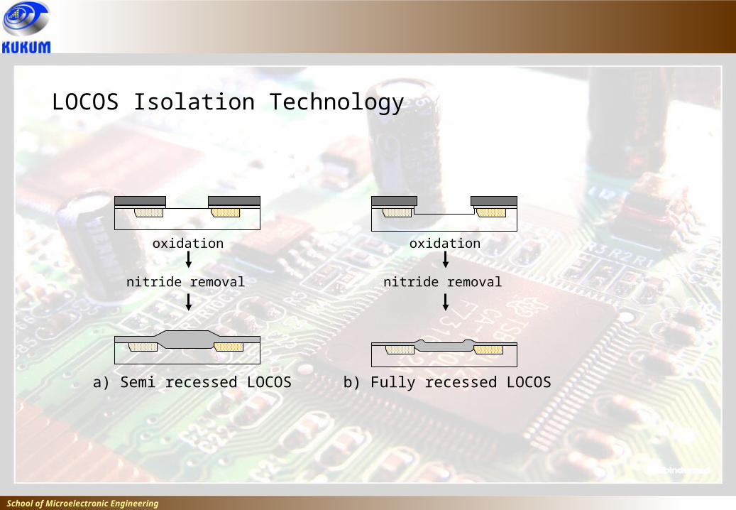
LOCOS Isolation Technology
oxidation
nitride removal
oxidation
nitride removal
a) Semi recessed LOCOS b) Fully recessed LOCOS

School of Microelectronic Engineering
Basic Semi-recessed LOCOS Process
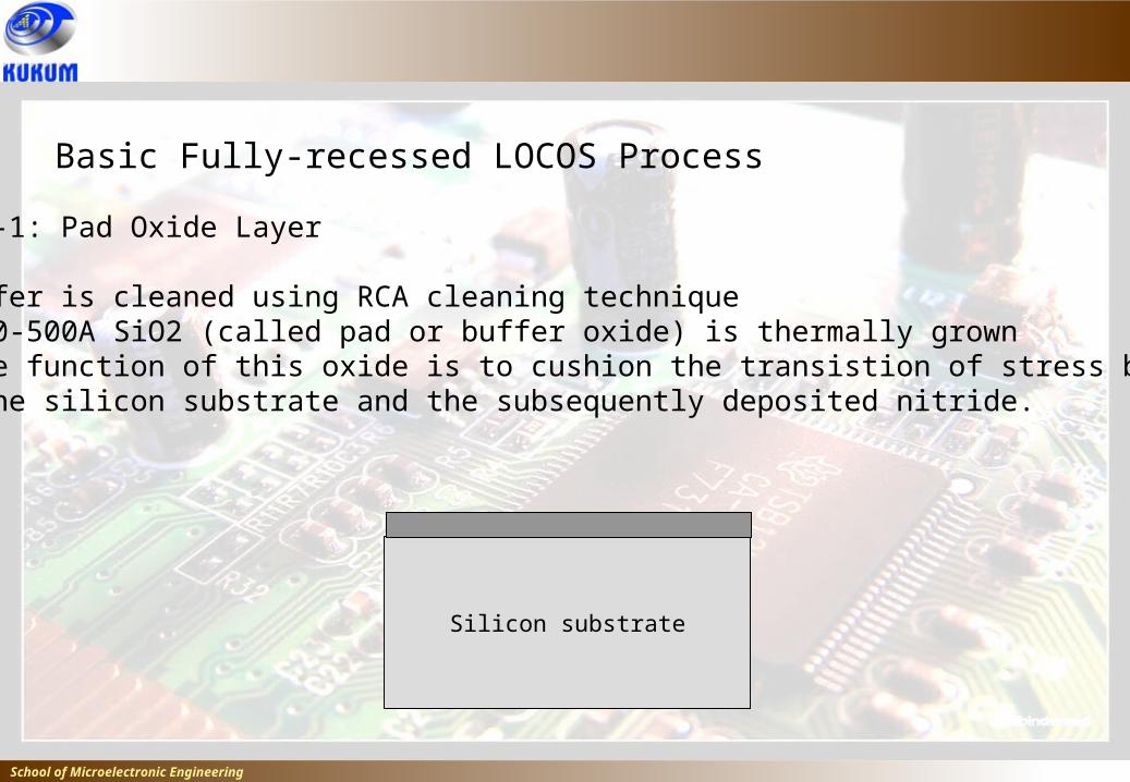
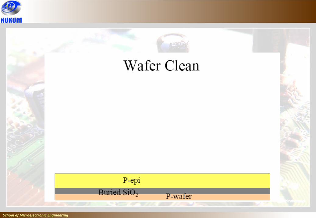
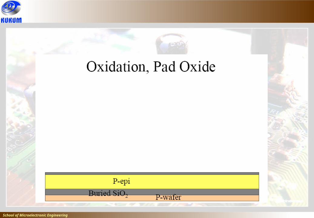
Step-1: Pad Oxide Layer
• Wafer is cleaned using RCA cleaning technique• 200-500A SiO2 (called pad or buffer oxide) is thermally grown• The function of this oxide is to cushion the transistion of stress between the silicon substrate and the subsequently deposited nitride.
Silicon substrate

School of Microelectronic Engineering
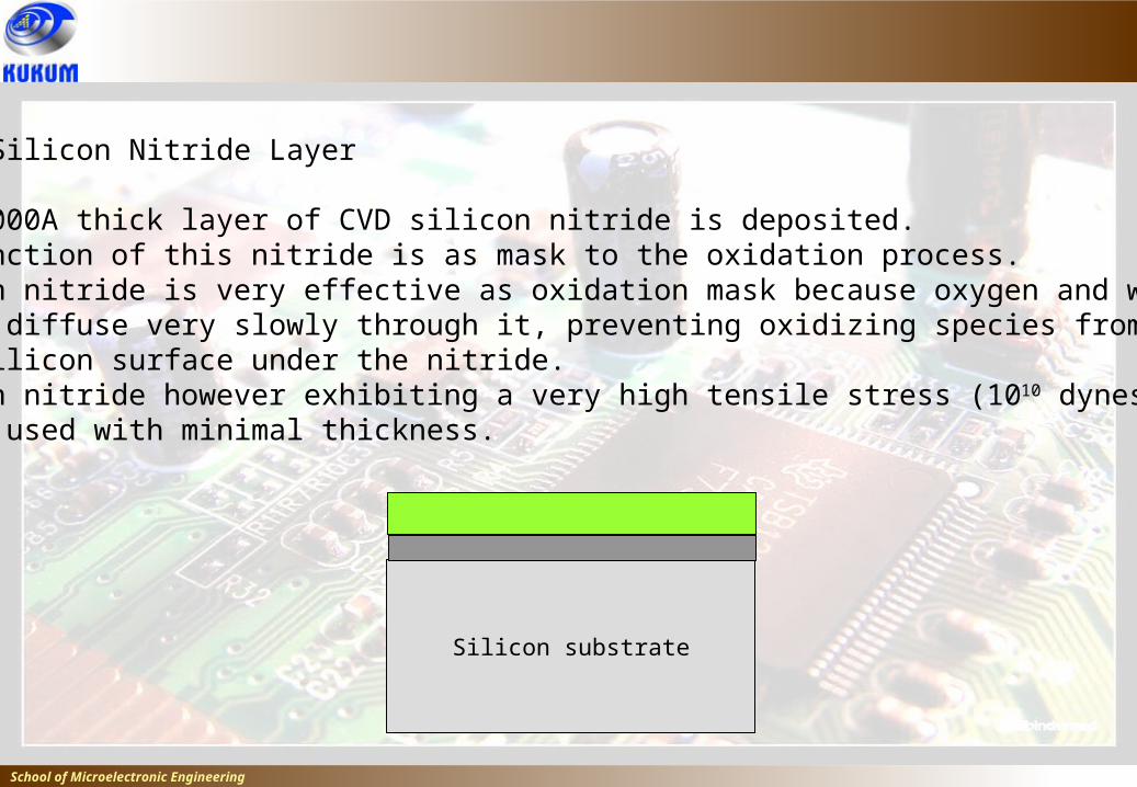
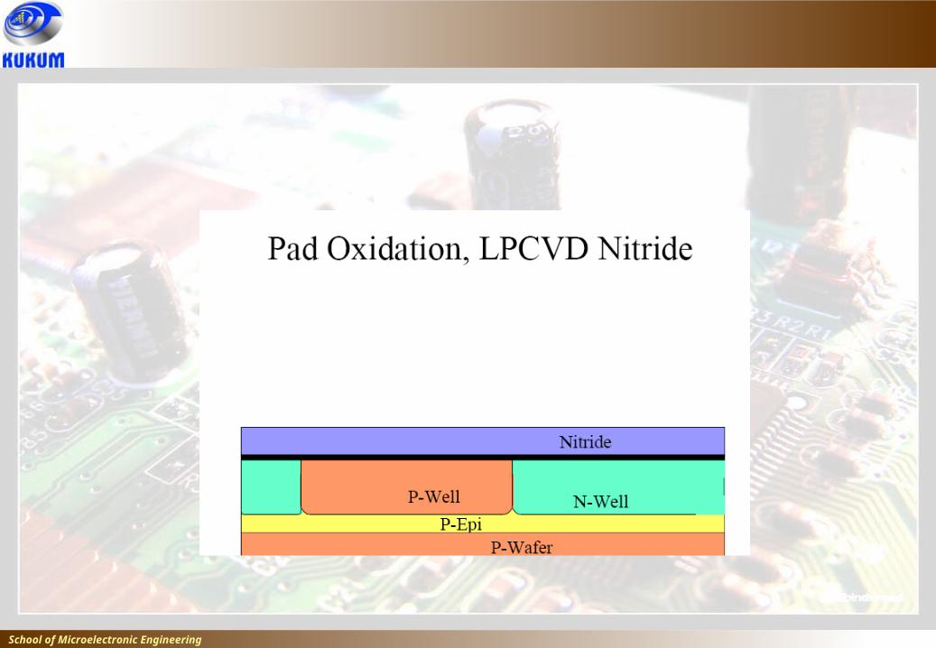
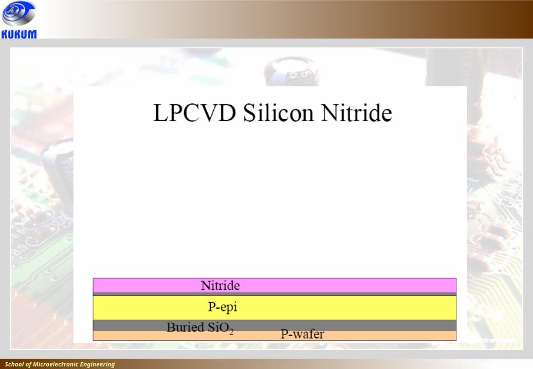
Step-2: Silicon Nitride Layer
• 1000-2000A thick layer of CVD silicon nitride is deposited.• The function of this nitride is as mask to the oxidation process.• Silicon nitride is very effective as oxidation mask because oxygen and water vapor diffuse very slowly through it, preventing oxidizing species from reaching the silicon surface under the nitride.• Silicon nitride however exhibiting a very high tensile stress (1010 dynes/cm2), hence used with minimal thickness.
Silicon substrate

School of Microelectronic Engineering
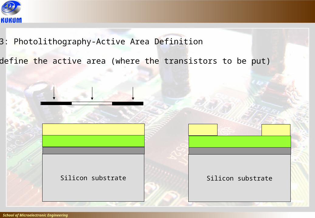
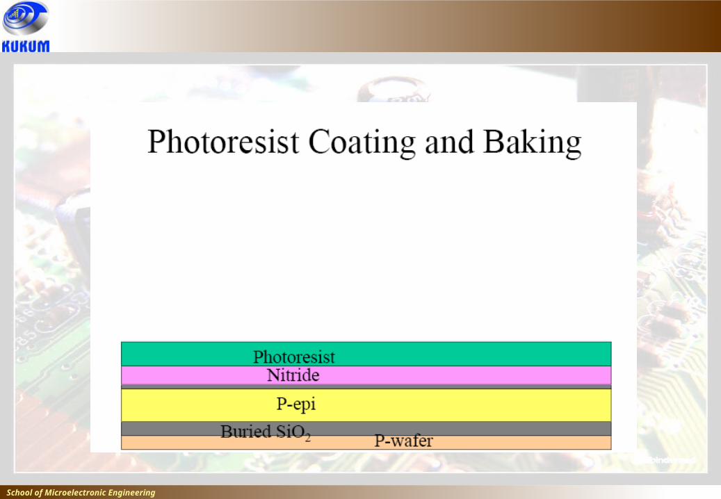
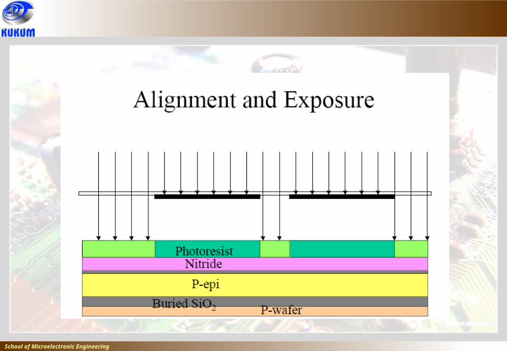
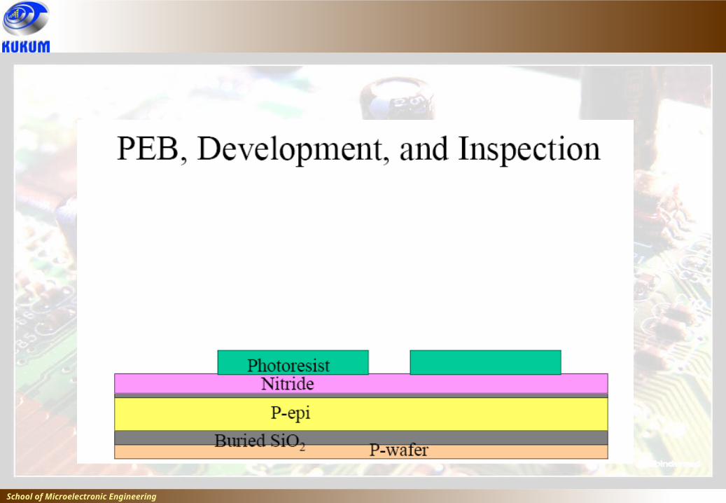
Step-3: Photolithography-Active Area Definition
• To define the active area (where the transistors to be put)
Silicon substrate Silicon substrate
School of Microelectronic Engineering
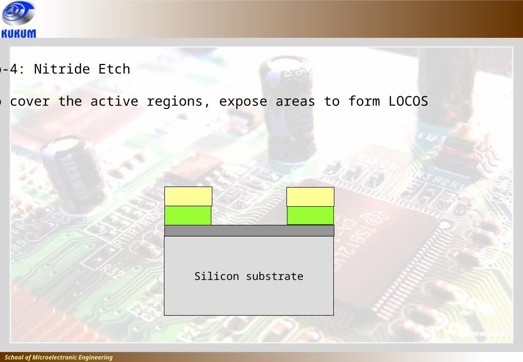
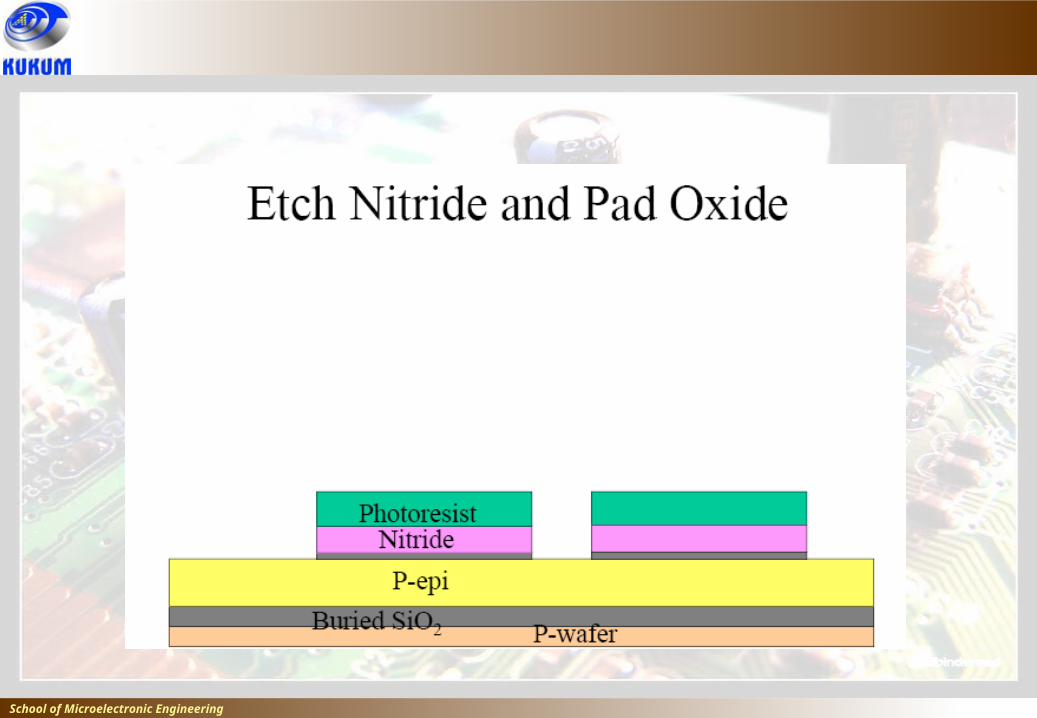
Step-4: Nitride Etch
• To cover the active regions, expose areas to form LOCOS
Silicon substrate
School of Microelectronic Engineering
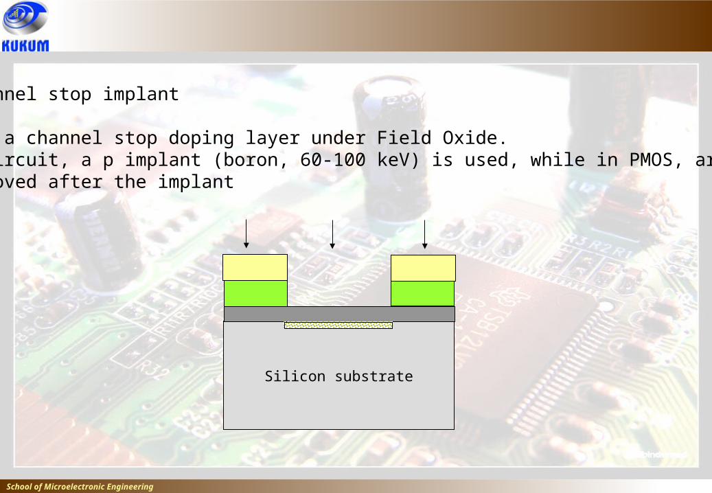
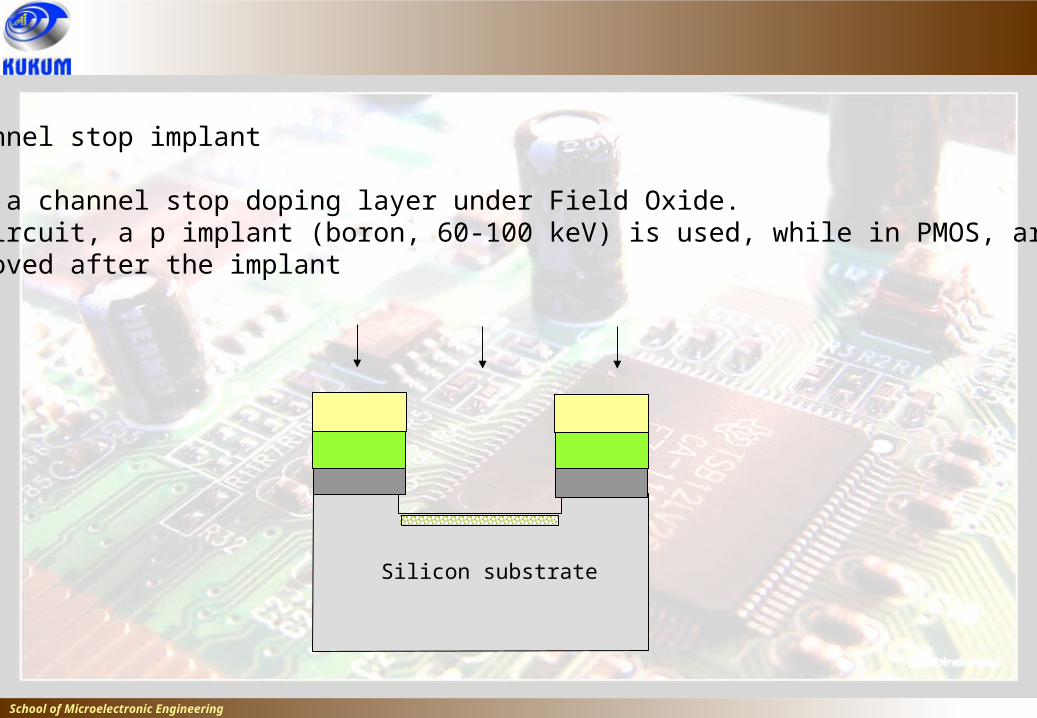
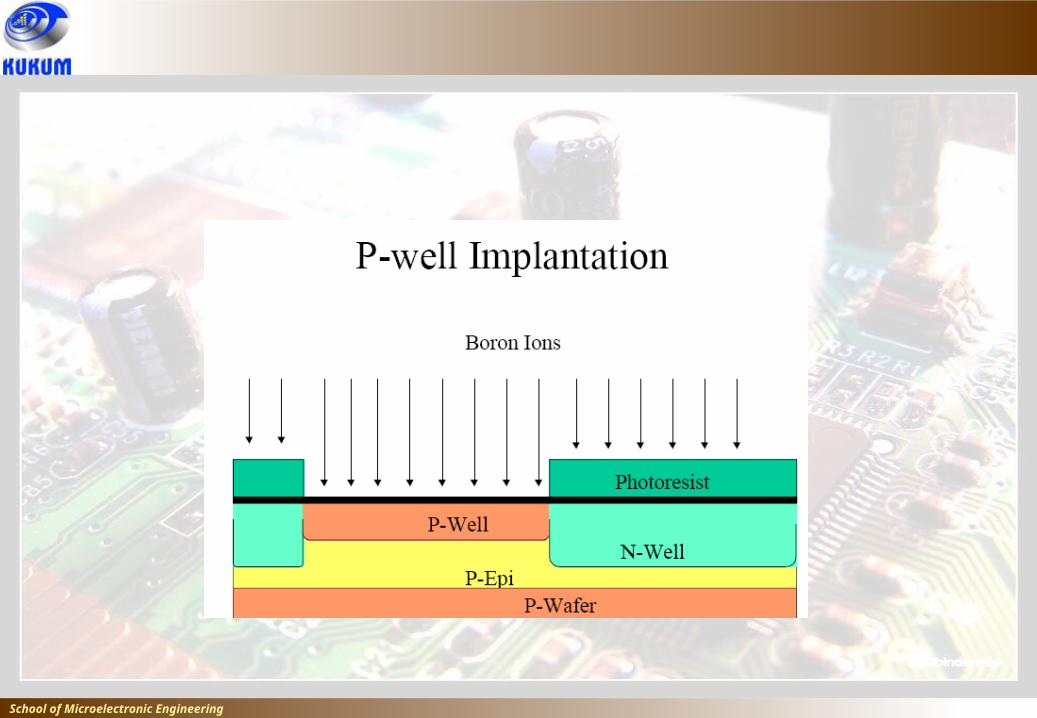
Step-5: Channel stop implant
• To create a channel stop doping layer under Field Oxide. • In NMOS circuit, a p implant (boron, 60-100 keV) is used, while in PMOS, arsenic is used.• PR is removed after the implant
Silicon substrate
School of Microelectronic Engineering
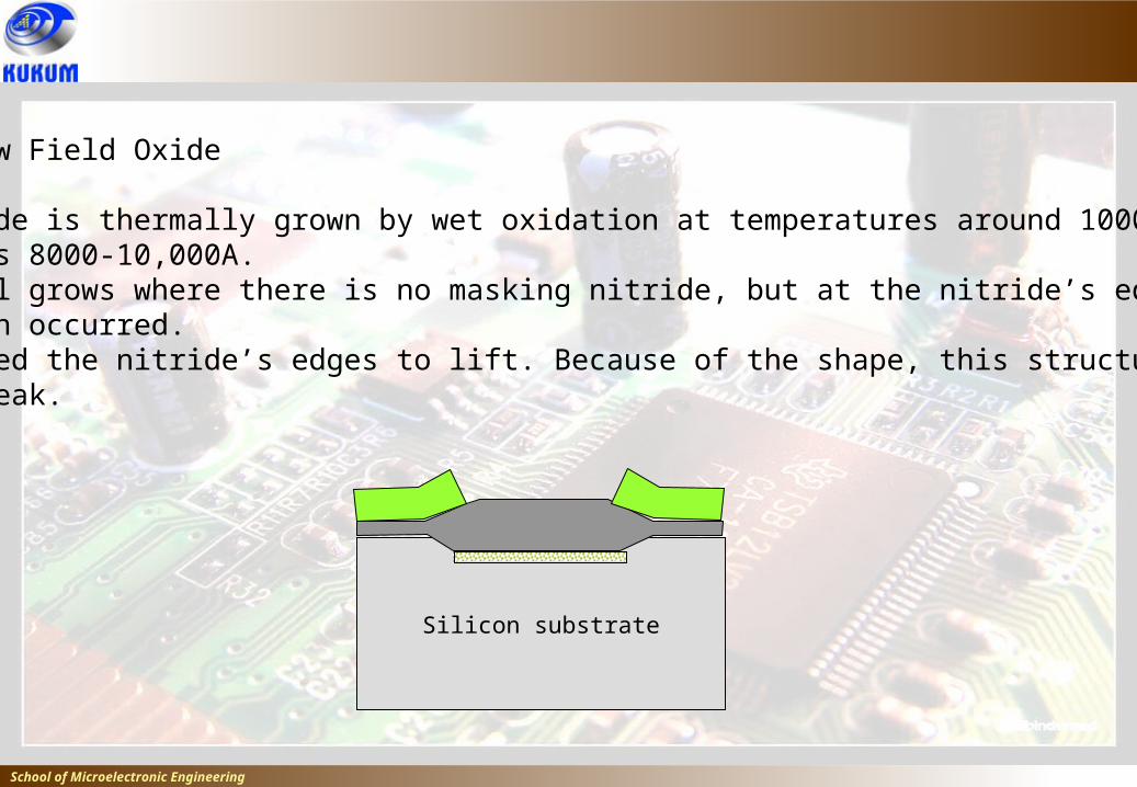
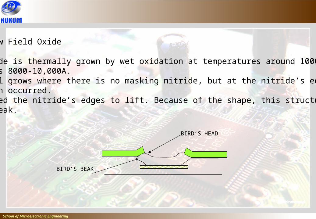
Step-6: Grow Field Oxide
• Field oxide is thermally grown by wet oxidation at temperatures around 1000C to the thickness 8000-10,000A. • Oxide will grows where there is no masking nitride, but at the nitride’s edges, some oxidation occurred.• This caused the nitride’s edges to lift. Because of the shape, this structure is called bird’s beak.
Silicon substrate
School of Microelectronic Engineering
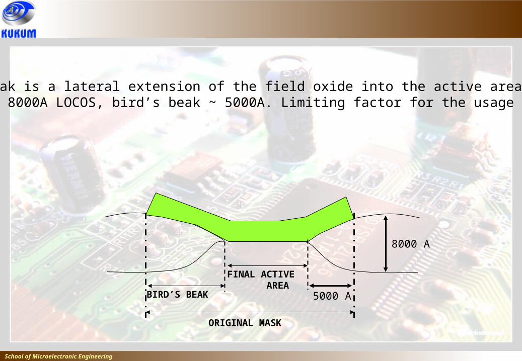
• The bird’s beak is a lateral extension of the field oxide into the active area of the devices.• For a typical 8000A LOCOS, bird’s beak ~ 5000A. Limiting factor for the usage of LOCOS.
ORIGINAL MASK
BIRD’S BEAK
FINAL ACTIVE AREA
8000 A
5000 A
School of Microelectronic Engineering
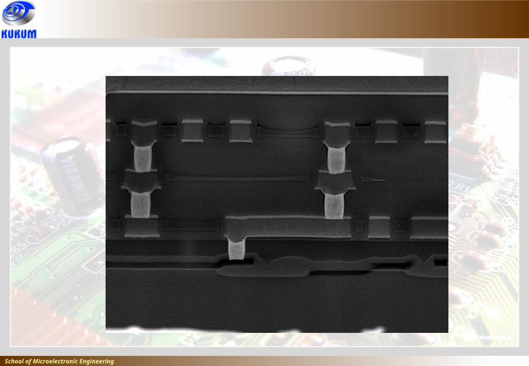
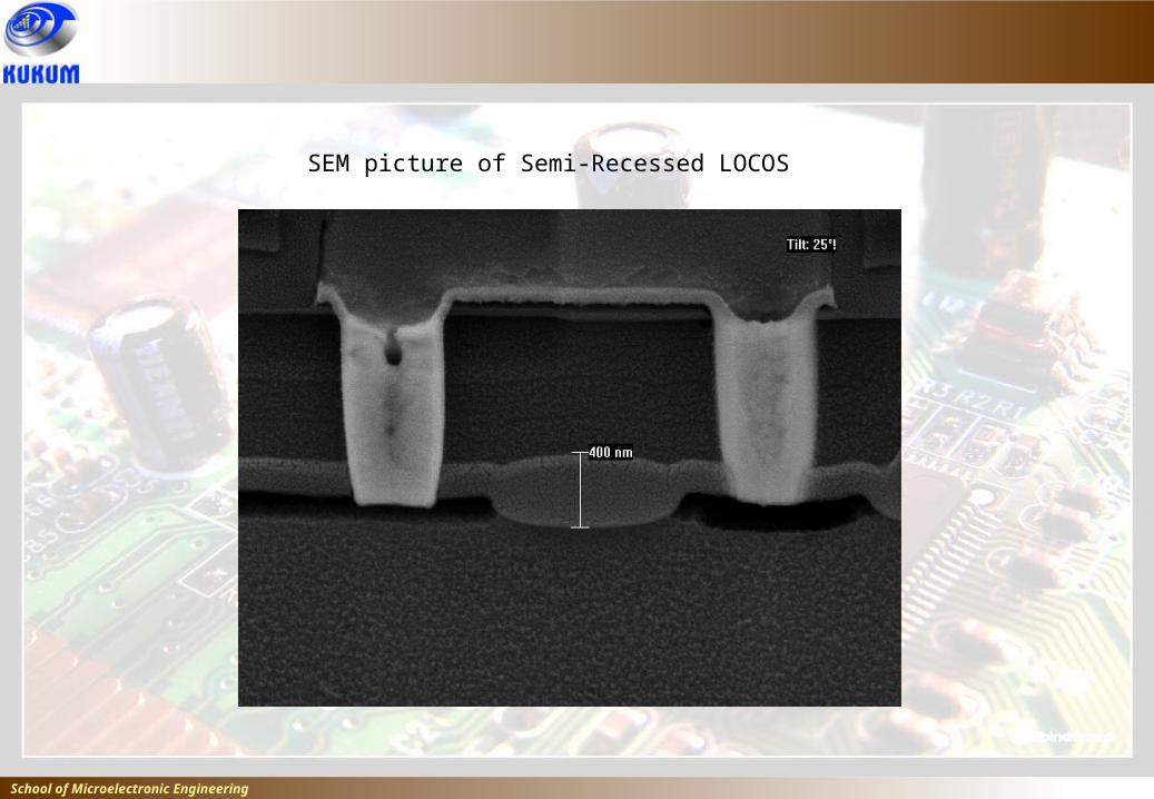
SEM picture of Semi-Recessed LOCOS
School of Microelectronic Engineering
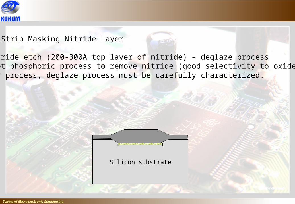
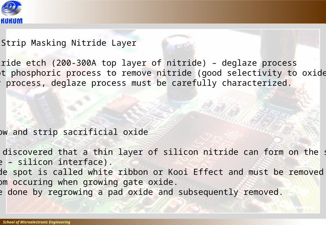
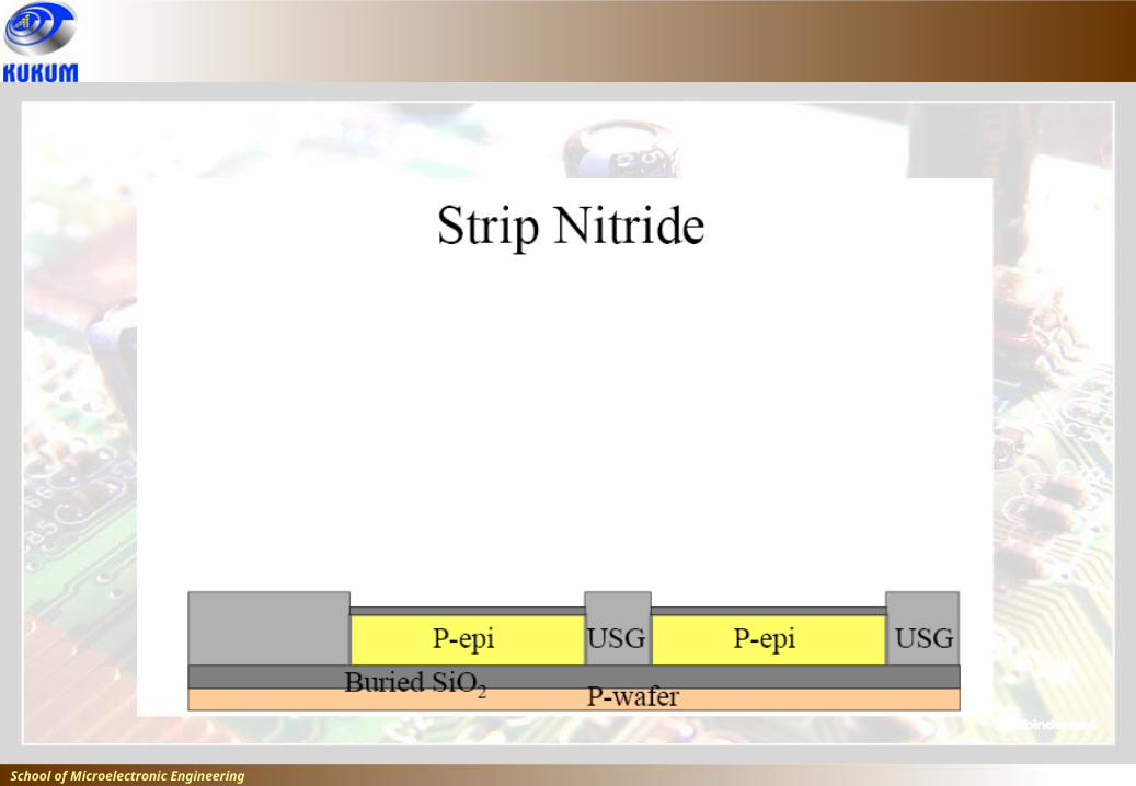
Step-7: Strip Masking Nitride Layer
• Oxynitride etch (200-300A top layer of nitride) – deglaze process• Wet hot phosphoric process to remove nitride (good selectivity to oxide)• Tricky process, deglaze process must be carefully characterized.
Silicon substrate
School of Microelectronic Engineering
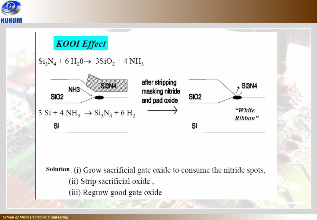
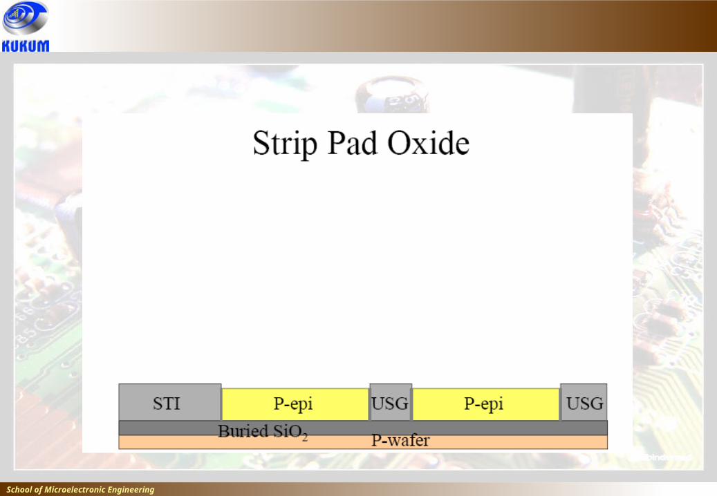
Step-8: Regrow and strip sacrificial oxide
• Kooi et al discovered that a thin layer of silicon nitride can form on the silicon surface (pad oxide – silicon interface).• This nitride spot is called white ribbon or Kooi Effect and must be removed to prevent defect from occuring when growing gate oxide.• This can be done by regrowing a pad oxide and subsequently removed.
School of Microelectronic Engineering
School of Microelectronic Engineering
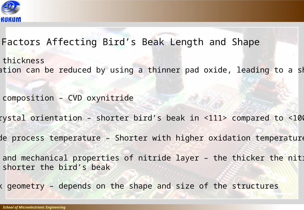
Factors Affecting Bird’s Beak Length and Shape
1) Pad oxide thicknessLateral oxidation can be reduced by using a thinner pad oxide, leading to a shorterbird’s beak.
2) Pad layer composition – CVD oxynitride
3) Silicon crystal orientation – shorter bird’s beak in <111> compared to <100>
4) Field oxide process temperature – Shorter with higher oxidation temperature.
5) Thickness and mechanical properties of nitride layer – the thicker the nitride, the shorter the bird’s beak
6) Mask stack geometry – depends on the shape and size of the structures
School of Microelectronic Engineering
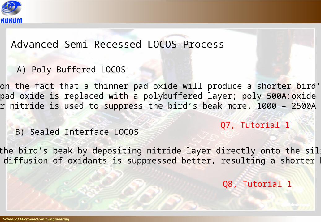
Advanced Semi-Recessed LOCOS Process
• Based on the fact that a thinner pad oxide will produce a shorter bird’s beak.• Usual pad oxide is replaced with a polybuffered layer; poly 500A:oxide 100A• Thicker nitride is used to suppress the bird’s beak more, 1000 – 2500A
A) Poly Buffered LOCOS
B) Sealed Interface LOCOS
• Reduce the bird’s beak by depositing nitride layer directly onto the silicon.• Lateral diffusion of oxidants is suppressed better, resulting a shorter bird’s beak.
Q7, Tutorial 1
Q8, Tutorial 1
School of Microelectronic Engineering
Basic Fully-recessed LOCOS Process
Step-1: Pad Oxide Layer
• Wafer is cleaned using RCA cleaning technique• 200-500A SiO2 (called pad or buffer oxide) is thermally grown• The function of this oxide is to cushion the transistion of stress between the silicon substrate and the subsequently deposited nitride.
Silicon substrate
School of Microelectronic Engineering
Step-2: Silicon Nitride Layer
• 1000-2000A thick layer of CVD silicon nitride is deposited.• The function of this nitride is as mask to the oxidation process.• Silicon nitride is very effective as oxidation mask because oxygen and water vapor diffuse very slowly through it, preventing oxidizing species from reaching the silicon surface under the nitride.• Silicon nitride however exhibiting a very high tensile stress (1010 dynes/cm2), hence used with minimal thickness.
Silicon substrate
School of Microelectronic Engineering
Step-3: Photolithography-Active Area Definition
• To define the active area (where the transistors to be put)
Silicon substrate Silicon substrate
School of Microelectronic Engineering
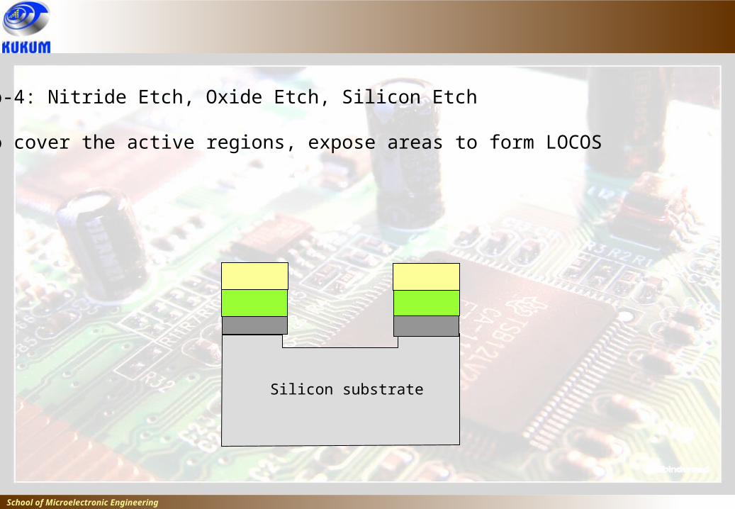
Step-4: Nitride Etch, Oxide Etch, Silicon Etch
• To cover the active regions, expose areas to form LOCOS
Silicon substrate
School of Microelectronic Engineering
Step-5: Channel stop implant
• To create a channel stop doping layer under Field Oxide. • In NMOS circuit, a p implant (boron, 60-100 keV) is used, while in PMOS, arsenic is used.• PR is removed after the implant
Silicon substrate
School of Microelectronic Engineering
BIRD’S BEAK
Step-6: Grow Field Oxide
• Field oxide is thermally grown by wet oxidation at temperatures around 1000C to the thickness 8000-10,000A. • Oxide will grows where there is no masking nitride, but at the nitride’s edges, some oxidation occurred.• This caused the nitride’s edges to lift. Because of the shape, this structure is called bird’s beak.
BIRD’S HEAD
School of Microelectronic Engineering
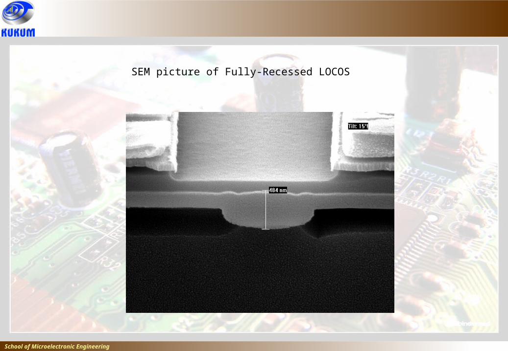
SEM picture of Fully-Recessed LOCOS
School of Microelectronic Engineering
Step-7: Strip Masking Nitride Layer
• Oxynitride etch (200-300A top layer of nitride) – deglaze process• Wet hot phosphoric process to remove nitride (good selectivity to oxide)• Tricky process, deglaze process must be carefully characterized.
Step-8: Regrow and strip sacrificial oxide
• Kooi et al discovered that a thin layer of silicon nitride can form on the silicon surface (pad oxide – silicon interface).• This nitride spot is called white ribbon or Kooi Effect and must be removed to prevent defect from occuring when growing gate oxide.• This can be done by regrowing a pad oxide and subsequently removed.
School of Microelectronic Engineering
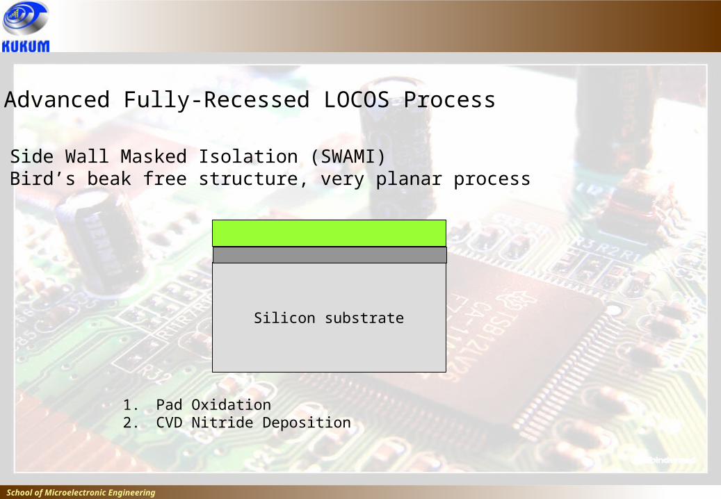
Advanced Fully-Recessed LOCOS Process
A) Side Wall Masked Isolation (SWAMI)• Bird’s beak free structure, very planar process
Silicon substrate
1. Pad Oxidation2. CVD Nitride Deposition
School of Microelectronic Engineering
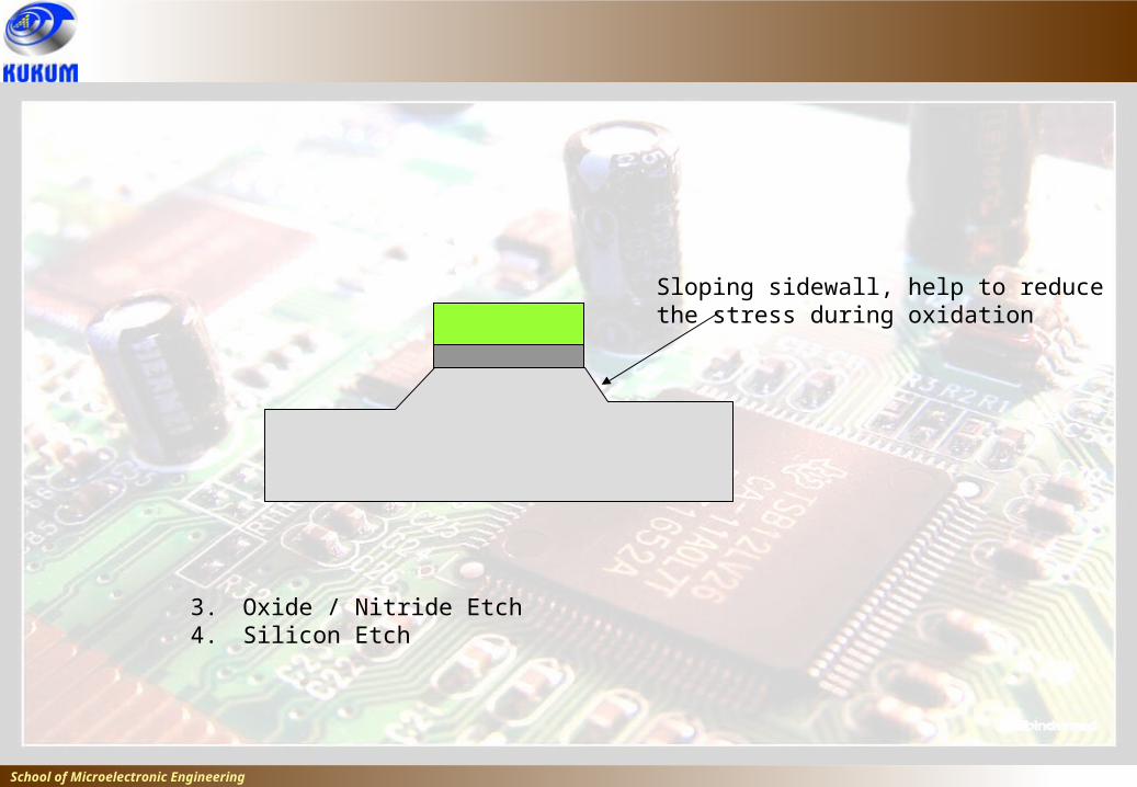
3. Oxide / Nitride Etch4. Silicon Etch
Sloping sidewall, help to reducethe stress during oxidation

School of Microelectronic Engineering
5. Second layer of pad oxide and nitride6. CVD Oxide

School of Microelectronic Engineering
7. Etch Oxide, Etch Nitride8. Field Oxidation9. Nitride / Oxide strip
ActiveLOCOS
School of Microelectronic Engineering
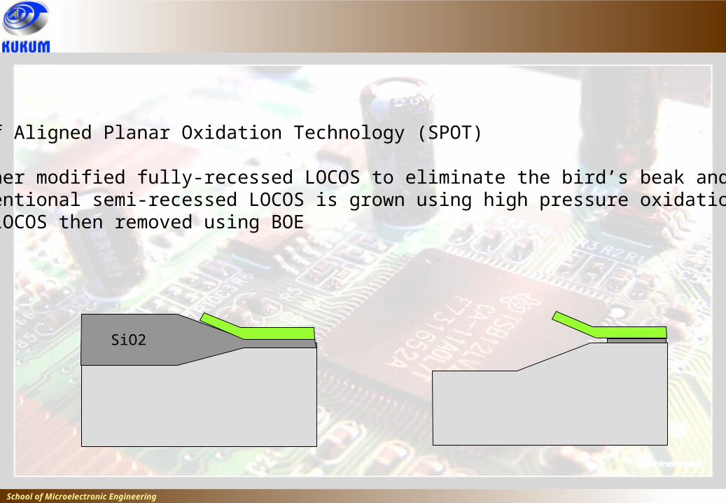
B) Self Aligned Planar Oxidation Technology (SPOT)
• Another modified fully-recessed LOCOS to eliminate the bird’s beak and head.• Conventional semi-recessed LOCOS is grown using high pressure oxidation. • The LOCOS then removed using BOE
SiO2
School of Microelectronic Engineering
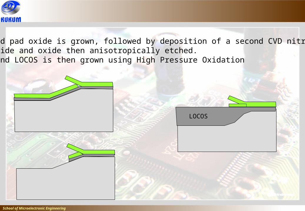
•Second pad oxide is grown, followed by deposition of a second CVD nitride• Nitride and oxide then anisotropically etched.• Second LOCOS is then grown using High Pressure Oxidation
LOCOS
School of Microelectronic Engineering
C) Fully Recessed Oxide (FUROX)
D) OSELO
E) ETC
School of Microelectronic Engineering
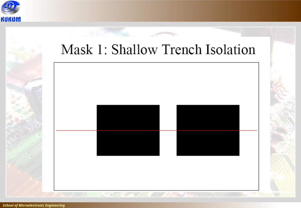
4 major applications• Locos replacement for isolation within the well (STI)• Isolation in bipolar (Moderate Trench)• Latch prevention in CMOS (Moderate Trench)• Trench capacitor in DRAM (Deep Trench)
3 categories• Shallow trench <1 um• Moderate 1-3 um• Deep >3um deep
AdvantagesIncrease the packing density tremendously
DisadvantagesComplex to fabricate, very expensive machinesPoor uniformity, Low throughput
Trench Isolation Technology
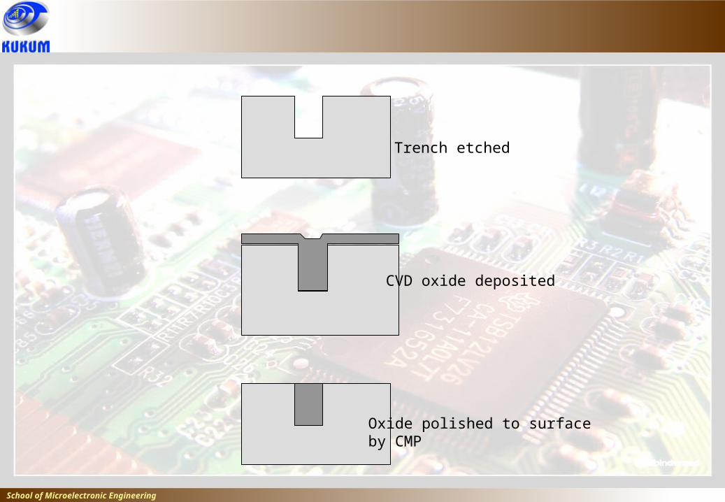
School of Microelectronic Engineering
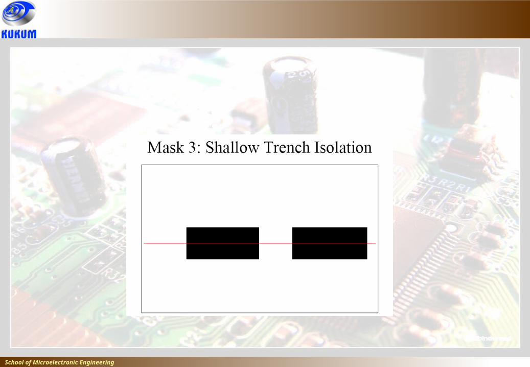
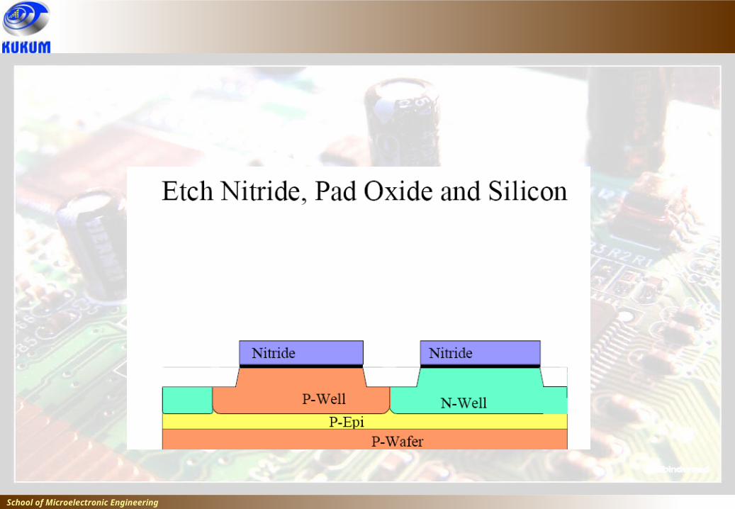
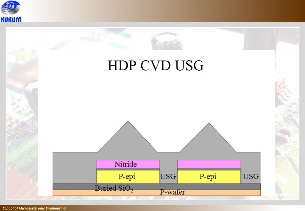
Trench etched
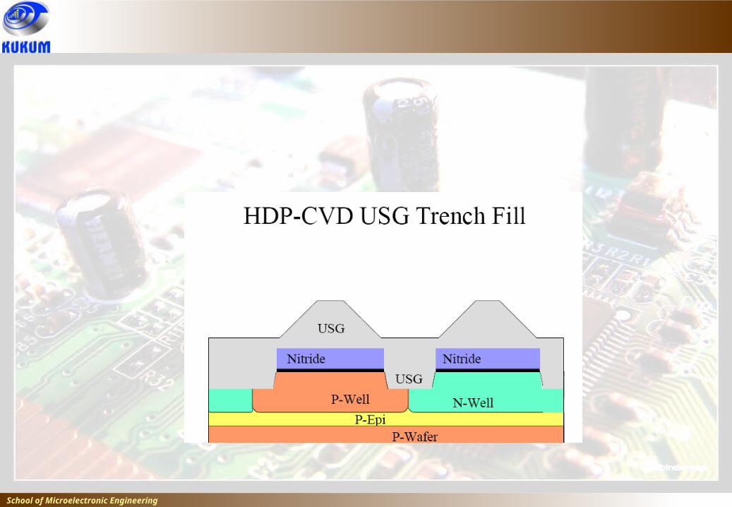
CVD oxide deposited
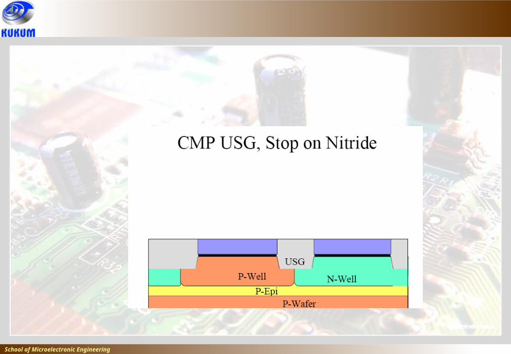
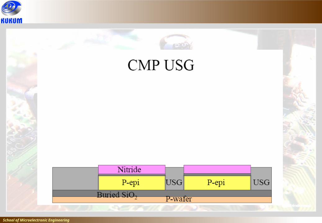
Oxide polished to surfaceby CMP
School of Microelectronic Engineering
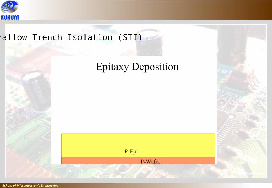
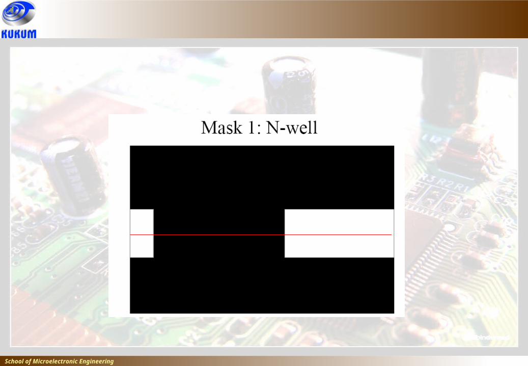
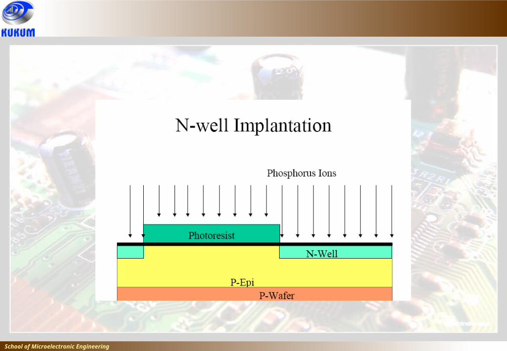
Shallow Trench Isolation (STI)
School of Microelectronic Engineering
School of Microelectronic Engineering
School of Microelectronic Engineering
School of Microelectronic Engineering
School of Microelectronic Engineering
School of Microelectronic Engineering
School of Microelectronic Engineering
School of Microelectronic Engineering
School of Microelectronic Engineering
School of Microelectronic Engineering
School of Microelectronic Engineering
School of Microelectronic Engineering
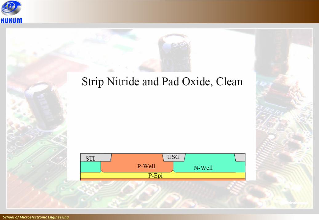
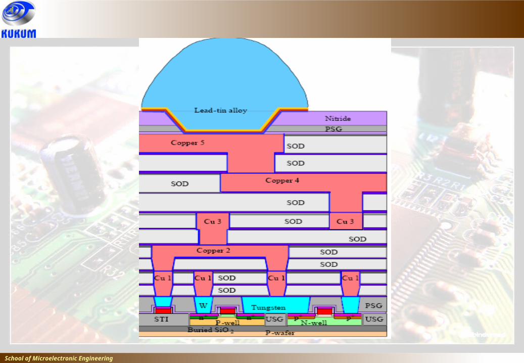
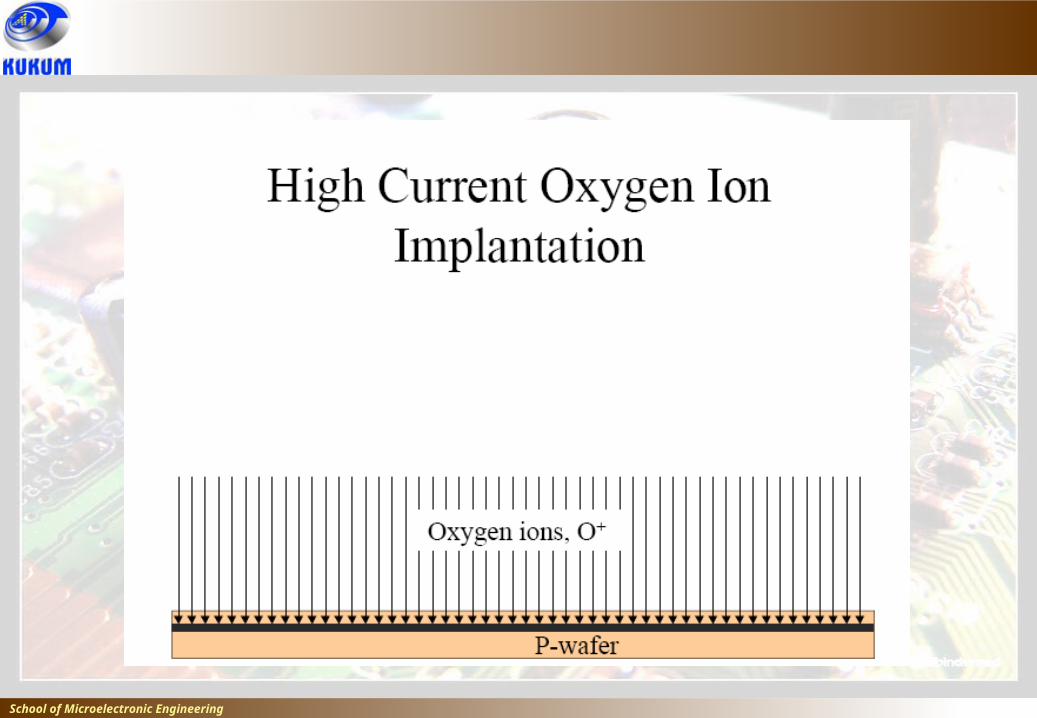
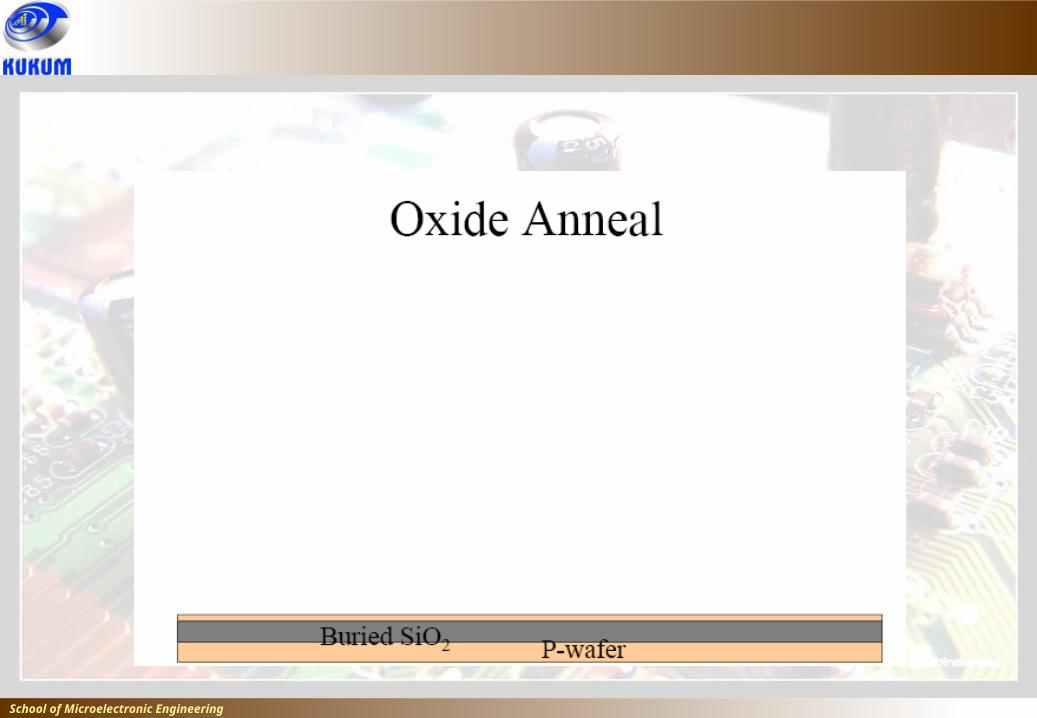
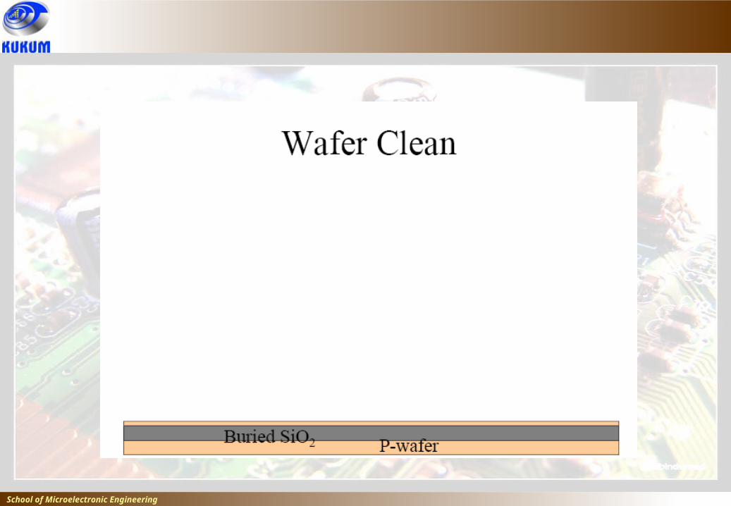
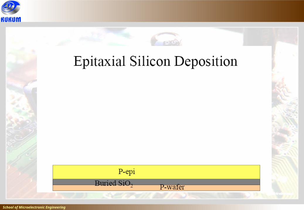
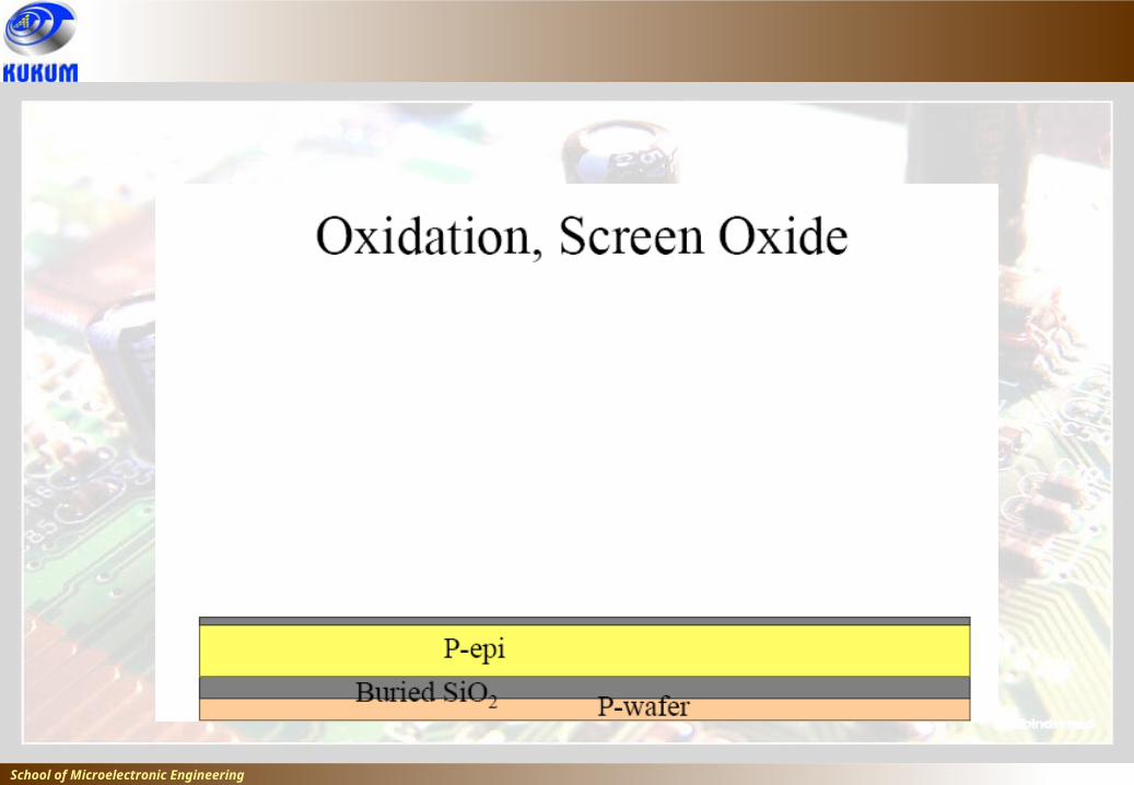
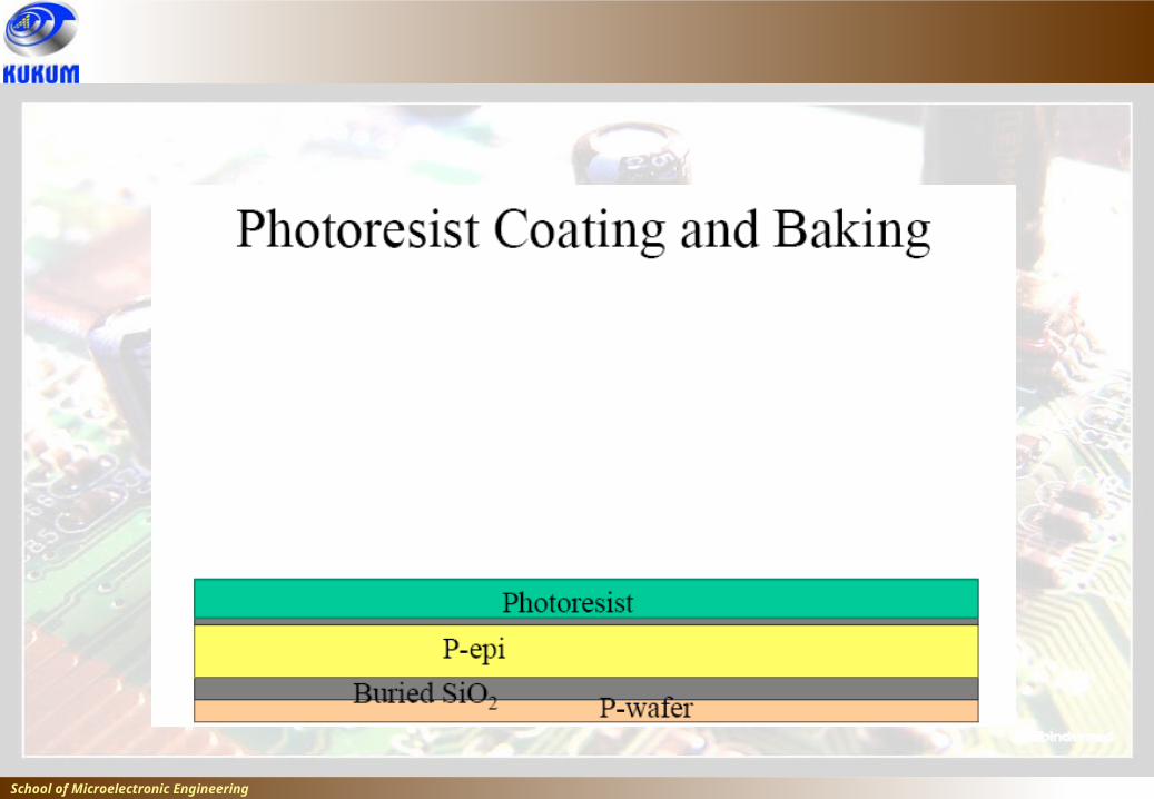
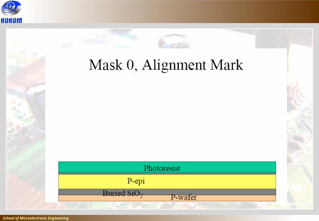
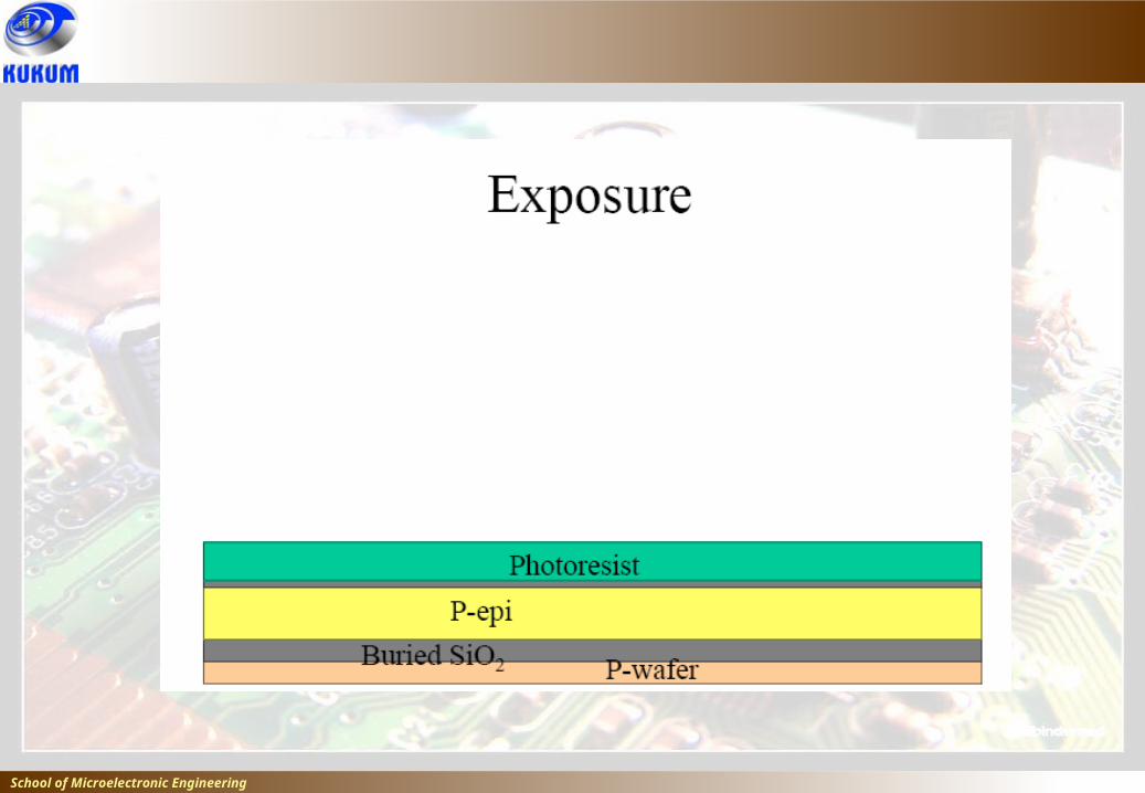
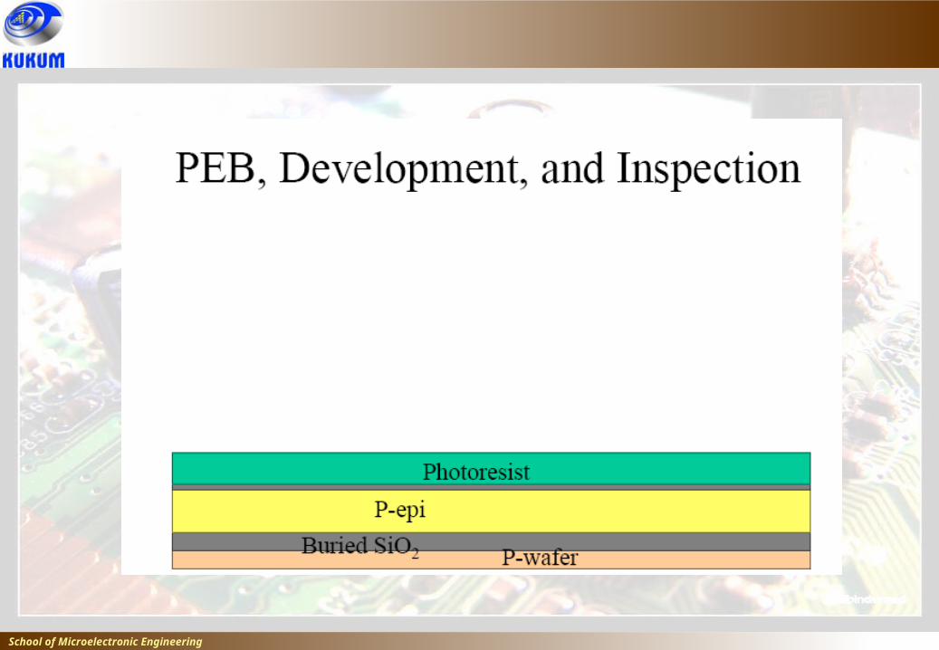
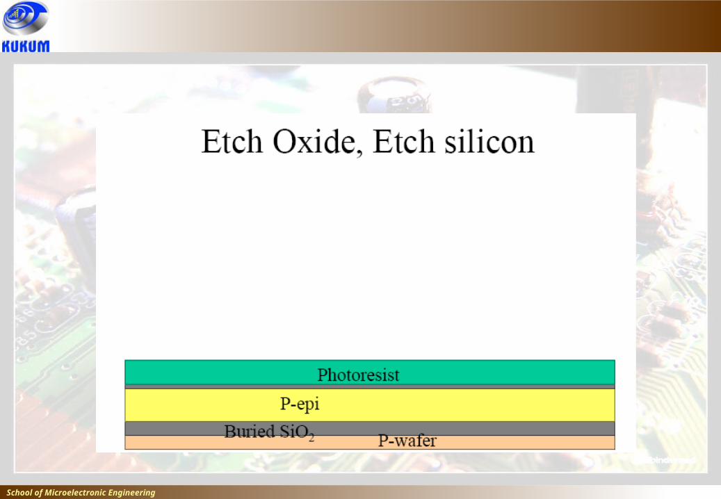
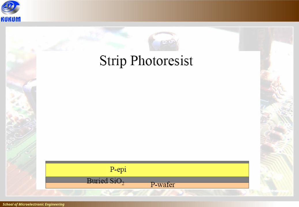
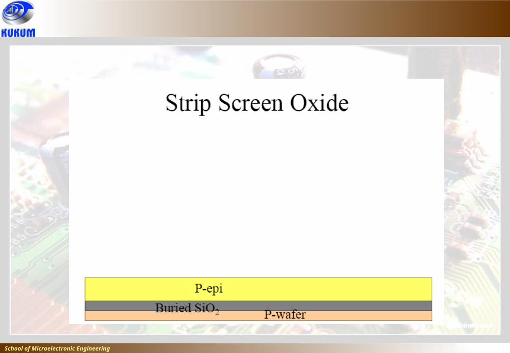
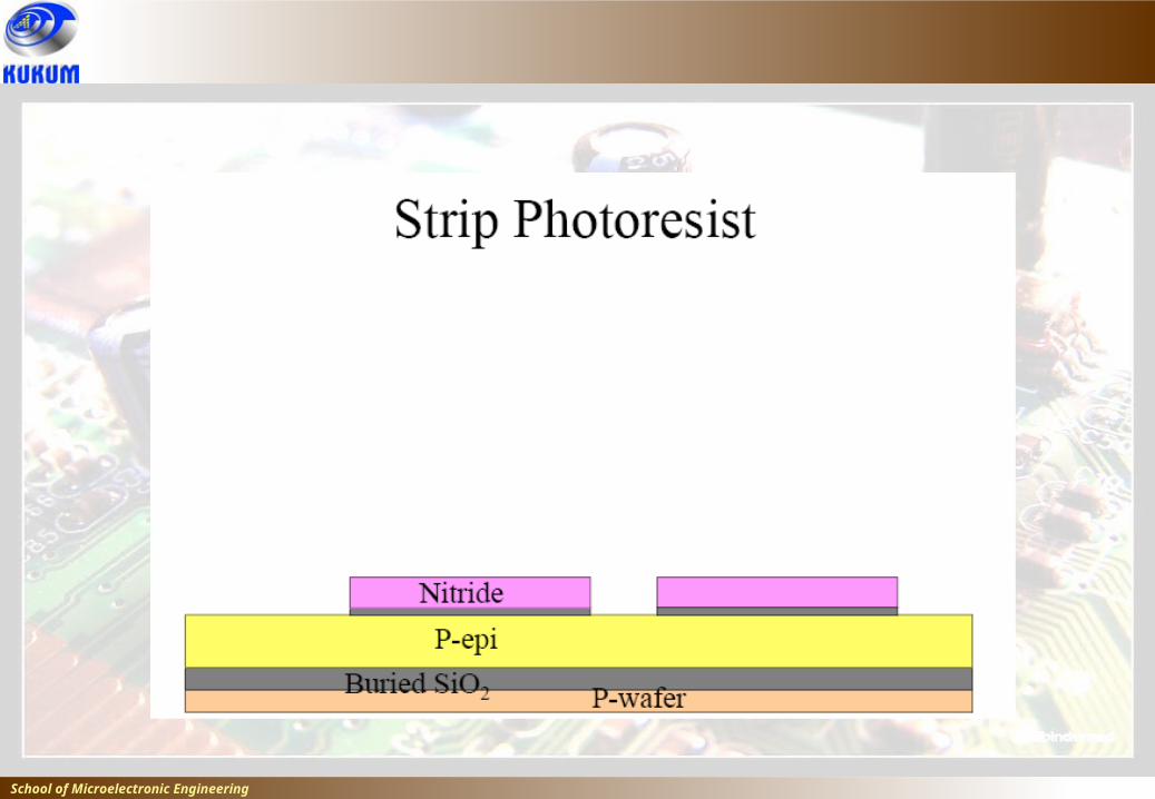
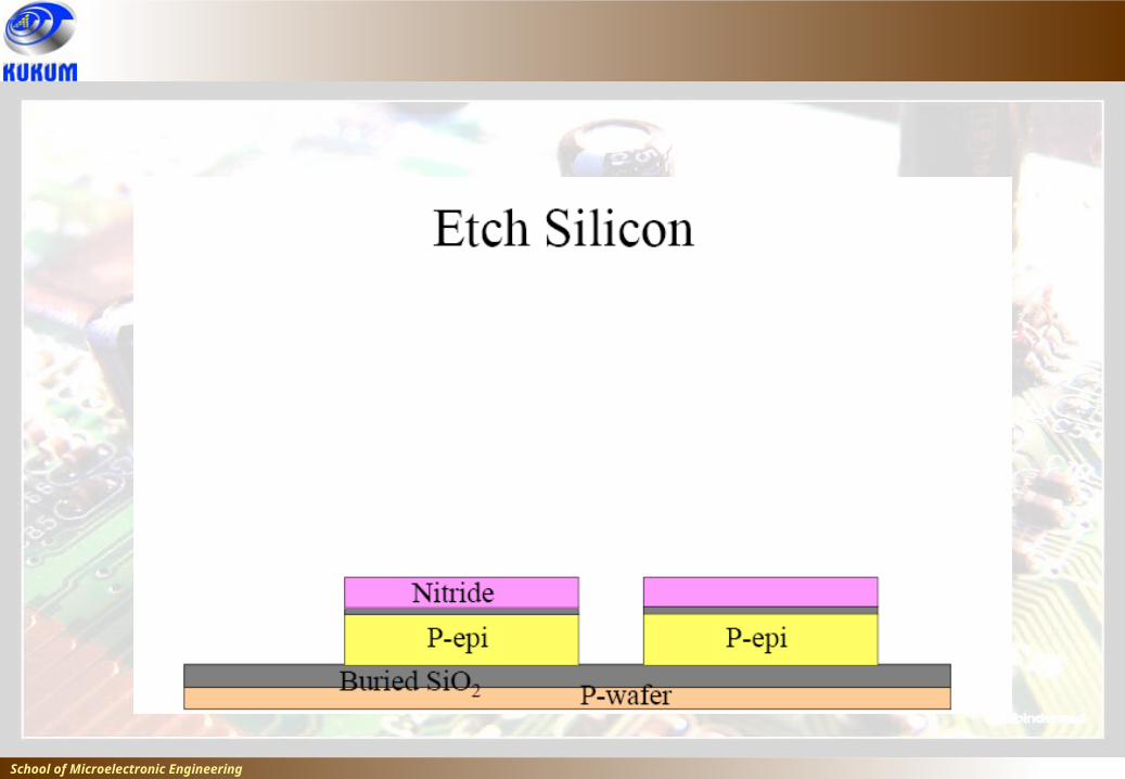
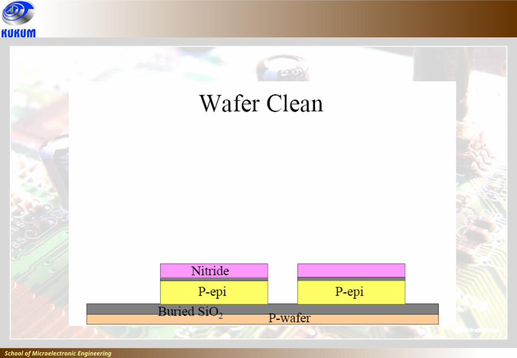
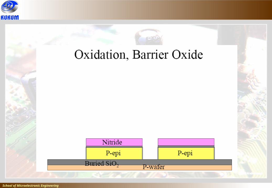
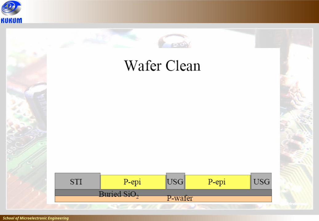
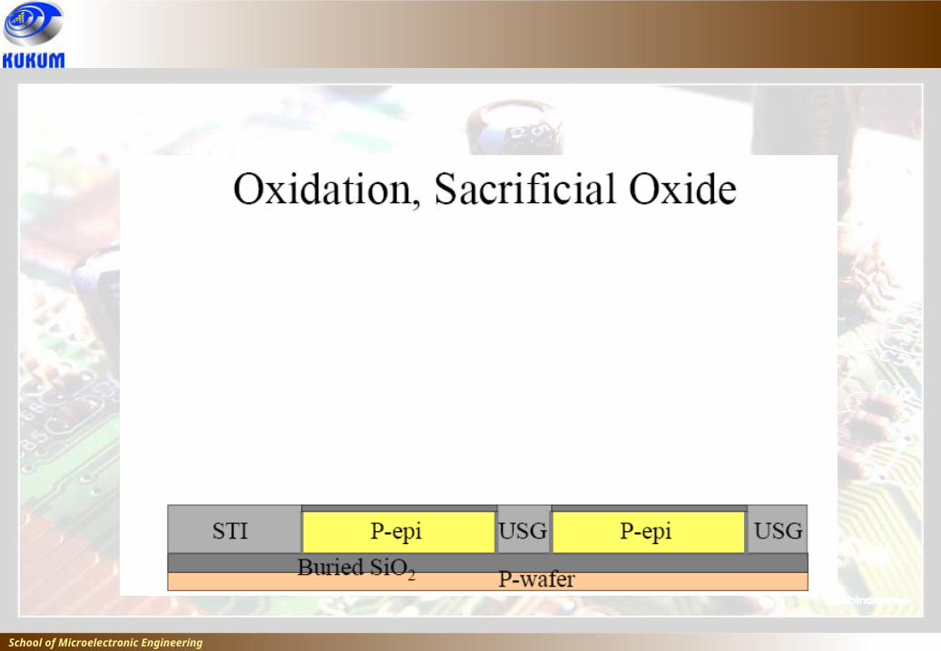
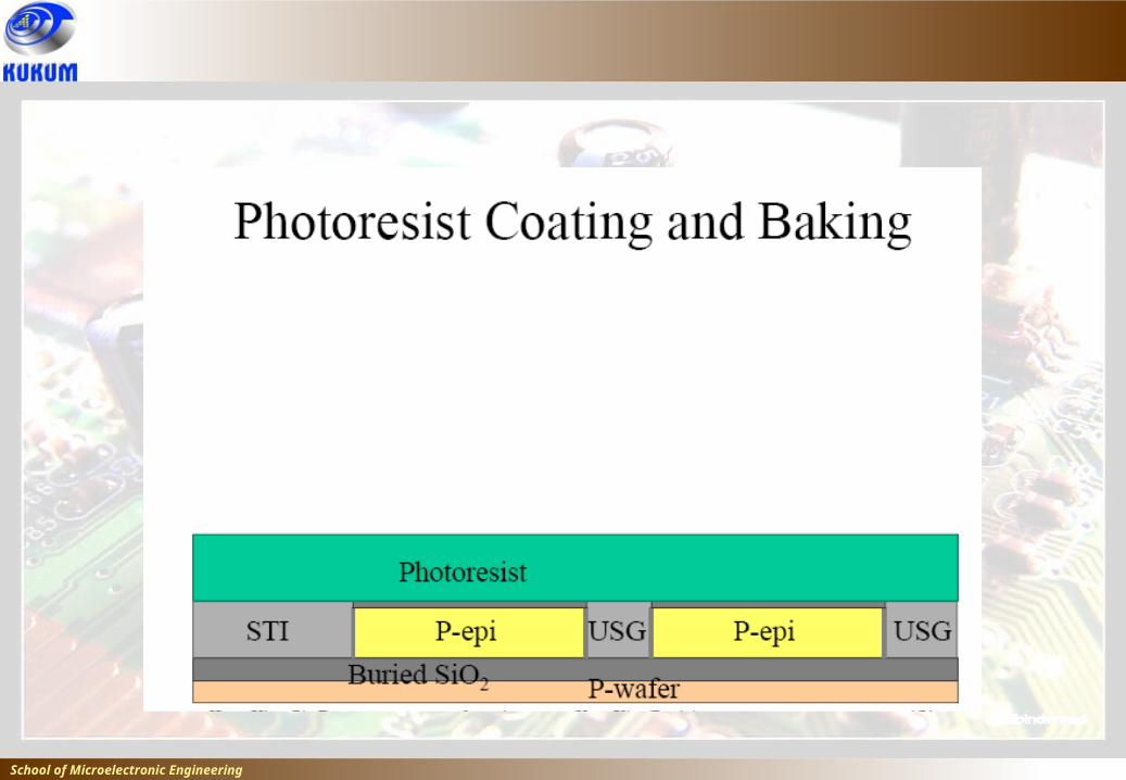
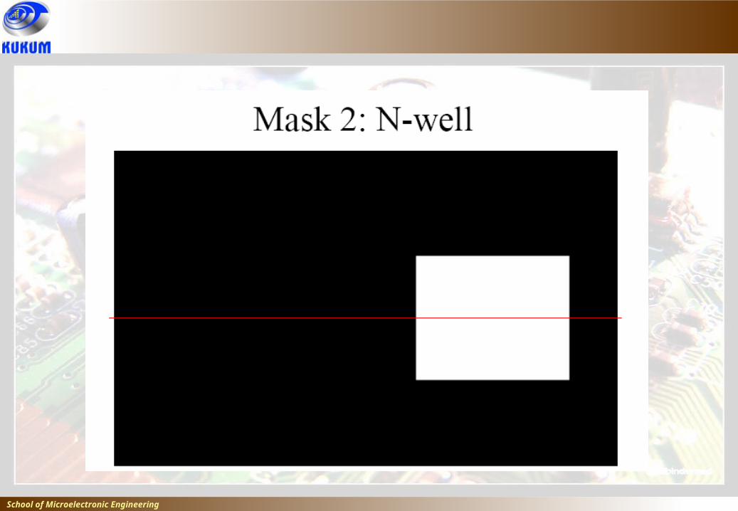
Silicon On Insulator (SOI) with STI Isolation Technology
• Completely isolate the transistor on silicon surface from the bulk silicon substrate.• Tremendously increase the packing density of IC chip• Mainstream isolation technology for high performance ICs for feature size below 0.13um process technology• Normally coupled with Copper Interconnect Technology and Low-k Interlevel
Dielectric.
School of Microelectronic Engineering
School of Microelectronic Engineering
School of Microelectronic Engineering
School of Microelectronic Engineering
School of Microelectronic Engineering
School of Microelectronic Engineering
School of Microelectronic Engineering
School of Microelectronic Engineering
School of Microelectronic Engineering
School of Microelectronic Engineering
School of Microelectronic Engineering
School of Microelectronic Engineering
School of Microelectronic Engineering
School of Microelectronic Engineering
School of Microelectronic Engineering
School of Microelectronic Engineering
School of Microelectronic Engineering
School of Microelectronic Engineering
School of Microelectronic Engineering
School of Microelectronic Engineering
School of Microelectronic Engineering
School of Microelectronic Engineering
School of Microelectronic Engineering
School of Microelectronic Engineering
School of Microelectronic Engineering
School of Microelectronic Engineering
School of Microelectronic Engineering
School of Microelectronic Engineering
School of Microelectronic Engineering
School of Microelectronic Engineering
School of Microelectronic Engineering
School of Microelectronic Engineering
School of Microelectronic Engineering
School of Microelectronic Engineering