sces598e –july 2004–revised march 2016 … · b dir 5 4 a 3 v cca v ccb product folder sample...
TRANSCRIPT
B
DIR5
4
A3
VCCA VCCB
Product
Folder
Sample &Buy
Technical
Documents
Tools &
Software
Support &Community
ReferenceDesign
An IMPORTANT NOTICE at the end of this data sheet addresses availability, warranty, changes, use in safety-critical applications,intellectual property matters and other important disclaimers. PRODUCTION DATA.
SN74AVCH1T45SCES598E –JULY 2004–REVISED MARCH 2016
SN74AVCH1T45 Single-Bit Dual-Supply Bus TransceiverWith Configurable Level-Shifting, Voltage Translation, and 3-State Outputs
1
1 Features1• Available in the Texas Instruments NanoStar™
and NanoFree™ Packages• Control Inputs (DIR) VIH and VIL Levels Are
Referenced to VCCA Voltage• Bus Hold on Data Inputs Eliminates the Need for
External Pullup and Pulldown Resistors• VCC Isolation• Fully Configurable Dual-Rail Design• I/Os Are 4.6-V Tolerant• Ioff Supports Partial-Power-Down Mode Operation• Typical Max Data Rates
– 500 Mbps (1.8-V to 3.3-V Translation)– 320 Mbps (<1.8-V to 3.3-V Translation)– 320 Mbps (Translate to 2.5 V or 1.8 V)– 280 Mbps (Translate to 1.5 V)– 240 Mbps (Translate to 1.2 V)
• Latch-Up Performance Exceeds 100 mA PerJESD 78, Class II
• ESD Protection Exceeds JESD 22– Human-Body Model (A114-A): 2000 V– Machine Model (A115-A): 200 V– Charged-Device Model (C101): 1000 V
2 Applications• Personal Electronics• Industrial• Enterprise• Telecommunications
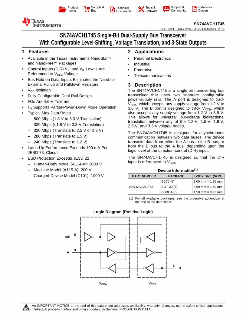
3 DescriptionThe SN74AVCH1T45 is a single-bit noninverting bustransceiver that uses two separate configurablepower-supply rails. The A port is designed to trackVCCA, which accepts any supply voltage from 1.2 V to3.6 V. The B port is designed to track VCCB, whichalso accepts any supply voltage from 1.2 V to 3.6 V.This allows for universal low-voltage bidirectionaltranslation between any of the 1.2-V, 1.5-V, 1.8-V,2.5-V, and 3.3-V voltage nodes.
The SN74AVCH1T45 is designed for asynchronouscommunication between two data buses. The devicetransmits data from either the A bus to the B bus, orfrom the B bus to the A bus, depending upon thelogic level at the direction-control (DIR) input.
The SN74AVCH1T45 is designed so that the DIRinput is referenced to VCCA.
Device Information(1)
PART NUMBER PACKAGE BODY SIZE (NOM)
SN74AVCH1T45SC70 (6) 2.00 mm × 1.25 mmSOT-23 (6) 2.90 mm × 1.60 mmDSBGA (6) 1.50 mm × 0.90 mm
(1) For all available packages, see the orderable addendum atthe end of the data sheet.
Logic Diagram (Positive Logic)
2
SN74AVCH1T45SCES598E –JULY 2004–REVISED MARCH 2016 www.ti.com
Product Folder Links: SN74AVCH1T45
Submit Documentation Feedback Copyright © 2004–2016, Texas Instruments Incorporated
Table of Contents1 Features .................................................................. 12 Applications ........................................................... 13 Description ............................................................. 14 Revision History..................................................... 25 Description (continued)......................................... 36 Pin Configuration and Functions ......................... 37 Specifications......................................................... 4
7.1 Absolute Maximum Ratings ...................................... 47.2 ESD Ratings.............................................................. 47.3 Recommended Operating Conditions....................... 47.4 Thermal Information .................................................. 57.5 Electrical Characteristics........................................... 67.6 Switching Characteristics, VCCA= 1.2 V .................... 87.7 Switching Characteristics, VCCA= 1.5 V ± 0.1 V........ 97.8 Switching Characteristics, VCCA= 1.8 V ± 0.15 V.... 107.9 Switching Characteristics, VCCA= 2.5 V ± 0.2 V...... 117.10 Switching Characteristics, VCCA= 3.3 V ± 0.3 V.... 127.11 Operating Characteristics...................................... 137.12 Typical Characteristics .......................................... 14
8 Parameter Measurement Information ................ 16
9 Detailed Description ............................................ 179.1 Overview ................................................................. 179.2 Functional Block Diagram ....................................... 179.3 Feature Description................................................. 179.4 Device Functional Modes........................................ 18
10 Application and Implementation........................ 1810.1 Application Information.......................................... 1810.2 Typical Applications .............................................. 18
11 Power Supply Recommendations ..................... 2112 Layout................................................................... 22
12.1 Layout Guidelines ................................................. 2212.2 Layout Example .................................................... 22
13 Device and Documentation Support ................. 2313.1 Documentation Support ........................................ 2313.2 Community Resources.......................................... 2313.3 Trademarks ........................................................... 2313.4 Electrostatic Discharge Caution............................ 2313.5 Glossary ................................................................ 23
14 Mechanical, Packaging, and OrderableInformation ........................................................... 23
4 Revision HistoryNOTE: Page numbers for previous revisions may differ from page numbers in the current version.
Changes from Revision D (January 2008) to Revision E Page
• Added ESD Ratings table, Feature Description section, Device Functional Modes, Application and Implementationsection, Power Supply Recommendations section, Layout section, Device and Documentation Support section, andMechanical, Packaging, and Orderable Information section. ................................................................................................. 1
3
2
1
4
5
6
A
GND
VCCA
B
DIR
VCCB
1
2
3
6
5
4
VCCA
GND
A
VCCB
DIR
B
3
SN74AVCH1T45www.ti.com SCES598E –JULY 2004–REVISED MARCH 2016
Product Folder Links: SN74AVCH1T45
Submit Documentation FeedbackCopyright © 2004–2016, Texas Instruments Incorporated
5 Description (continued)Active bus-hold circuitry holds unused or undriven inputs at a valid logic state. Use of pullup or pulldown resistorswith the bus-hold circuitry is not recommended.
This device is fully specified for partial-power-down applications using Ioff. The Ioff circuitry disables the outputs,preventing damaging current backflow through the device.
The VCC isolation feature ensures that if either VCCA or VCCB is at GND, then the outputs are in the high-impedance state. The bus-hold circuitry on the powered-up side always stays active.
NanoFree package technology is a major breakthrough in IC packaging concepts, using the die as the package.
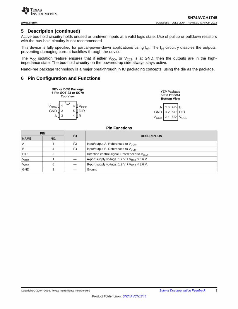
6 Pin Configuration and Functions
DBV or DCK Package6-Pin SOT-23 or SC70
Top ViewYZP Package6-Pin DSBGABottom View
Pin FunctionsPIN
I/O DESCRIPTIONNAME NO.A 3 I/O Input/output A. Referenced to VCCA.B 4 I/O Input/output B. Referenced to VCCB.DIR 5 I Direction control signal. Referenced to VCCA.VCCA 1 — A-port supply voltage. 1.2 V ≤ VCCA ≤ 3.6 VVCCB 6 — B-port supply voltage. 1.2 V ≤ VCCB ≤ 3.6 V.GND 2 — Ground
4
SN74AVCH1T45SCES598E –JULY 2004–REVISED MARCH 2016 www.ti.com
Product Folder Links: SN74AVCH1T45
Submit Documentation Feedback Copyright © 2004–2016, Texas Instruments Incorporated
(1) Stresses beyond those listed under Absolute Maximum Ratings may cause permanent damage to the device. These are stress ratingsonly, which do not imply functional operation of the device at these or any other conditions beyond those indicated under RecommendedOperating Conditions. Exposure to absolute-maximum-rated conditions for extended periods may affect device reliability.
(2) The input voltage and output negative-voltage ratings may be exceeded if the input and output current ratings are observed.(3) The output positive-voltage rating may be exceeded up to 4.6 V maximum if the output current rating is observed.
7 Specifications
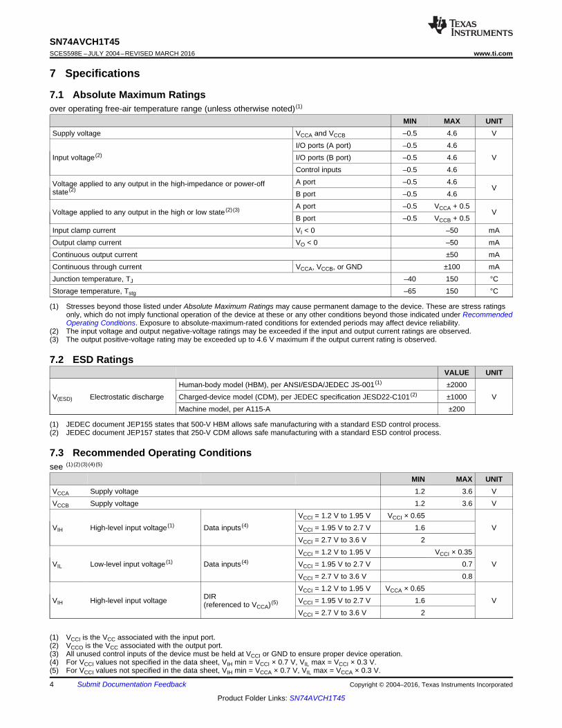
7.1 Absolute Maximum Ratingsover operating free-air temperature range (unless otherwise noted) (1)
MIN MAX UNITSupply voltage VCCA and VCCB –0.5 4.6 V
Input voltage (2)
I/O ports (A port) –0.5 4.6VI/O ports (B port) –0.5 4.6
Control inputs –0.5 4.6
Voltage applied to any output in the high-impedance or power-offstate (2)
A port –0.5 4.6V
B port –0.5 4.6
Voltage applied to any output in the high or low state (2) (3) A port –0.5 VCCA + 0.5V
B port –0.5 VCCB + 0.5Input clamp current VI < 0 –50 mAOutput clamp current VO < 0 –50 mAContinuous output current ±50 mAContinuous through current VCCA, VCCB, or GND ±100 mAJunction temperature, TJ –40 150 °CStorage temperature, Tstg –65 150 °C
(1) JEDEC document JEP155 states that 500-V HBM allows safe manufacturing with a standard ESD control process.(2) JEDEC document JEP157 states that 250-V CDM allows safe manufacturing with a standard ESD control process.
7.2 ESD RatingsVALUE UNIT
V(ESD) Electrostatic dischargeHuman-body model (HBM), per ANSI/ESDA/JEDEC JS-001 (1) ±2000
VCharged-device model (CDM), per JEDEC specification JESD22-C101 (2) ±1000Machine model, per A115-A ±200
(1) VCCI is the VCC associated with the input port.(2) VCCO is the VCC associated with the output port.(3) All unused control inputs of the device must be held at VCCI or GND to ensure proper device operation.(4) For VCCI values not specified in the data sheet, VIH min = VCCI × 0.7 V, VIL max = VCCI × 0.3 V.(5) For VCCI values not specified in the data sheet, VIH min = VCCA × 0.7 V, VIL max = VCCA × 0.3 V.
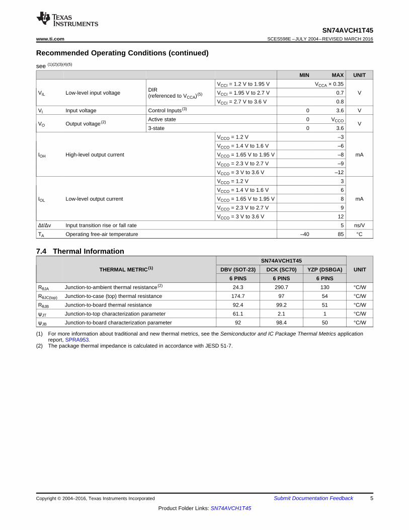
7.3 Recommended Operating Conditionssee (1) (2) (3) (4) (5)
MIN MAX UNITVCCA Supply voltage 1.2 3.6 VVCCB Supply voltage 1.2 3.6 V
VIH High-level input voltage (1) Data inputs (4)
VCCI = 1.2 V to 1.95 V VCCI × 0.65VVCCI = 1.95 V to 2.7 V 1.6
VCCI = 2.7 V to 3.6 V 2
VIL Low-level input voltage (1) Data inputs (4)
VCCI = 1.2 V to 1.95 V VCCI × 0.35VVCCI = 1.95 V to 2.7 V 0.7
VCCI = 2.7 V to 3.6 V 0.8
VIH High-level input voltage DIR(referenced to VCCA)(5)
VCCI = 1.2 V to 1.95 V VCCA × 0.65VVCCI = 1.95 V to 2.7 V 1.6
VCCI = 2.7 V to 3.6 V 2
5
SN74AVCH1T45www.ti.com SCES598E –JULY 2004–REVISED MARCH 2016
Product Folder Links: SN74AVCH1T45
Submit Documentation FeedbackCopyright © 2004–2016, Texas Instruments Incorporated
Recommended Operating Conditions (continued)see (1)(2)(3)(4)(5)
MIN MAX UNIT
VIL Low-level input voltage DIR(referenced to VCCA)(5)
VCCI = 1.2 V to 1.95 V VCCA × 0.35VVCCI = 1.95 V to 2.7 V 0.7
VCCI = 2.7 V to 3.6 V 0.8VI Input voltage Control Inputs (3) 0 3.6 V
VO Output voltage (2) Active state 0 VCCO V3-state 0 3.6
IOH High-level output current
VCCO = 1.2 V –3
mAVCCO = 1.4 V to 1.6 V –6VCCO = 1.65 V to 1.95 V –8VCCO = 2.3 V to 2.7 V –9VCCO = 3 V to 3.6 V –12
IOL Low-level output current
VCCO = 1.2 V 3
mAVCCO = 1.4 V to 1.6 V 6VCCO = 1.65 V to 1.95 V 8VCCO = 2.3 V to 2.7 V 9VCCO = 3 V to 3.6 V 12
Δt/Δv Input transition rise or fall rate 5 ns/VTA Operating free-air temperature –40 85 °C
(1) For more information about traditional and new thermal metrics, see the Semiconductor and IC Package Thermal Metrics applicationreport, SPRA953.
(2) The package thermal impedance is calculated in accordance with JESD 51-7.
7.4 Thermal Information
THERMAL METRIC (1)SN74AVCH1T45
UNITDBV (SOT-23) DCK (SC70) YZP (DSBGA)6 PINS 6 PINS 6 PINS
RθJA Junction-to-ambient thermal resistance (2) 24.3 290.7 130 °C/WRθJC(top) Junction-to-case (top) thermal resistance 174.7 97 54 °C/WRθJB Junction-to-board thermal resistance 92.4 99.2 51 °C/WψJT Junction-to-top characterization parameter 61.1 2.1 1 °C/WψJB Junction-to-board characterization parameter 92 98.4 50 °C/W

6
SN74AVCH1T45SCES598E –JULY 2004–REVISED MARCH 2016 www.ti.com
Product Folder Links: SN74AVCH1T45
Submit Documentation Feedback Copyright © 2004–2016, Texas Instruments Incorporated
(1) VCCO is the VCC associated with the output port.(2) VCCI is the VCC associated with the input port.(3) An external driver must source at least IBHLO to switch this node from low to high.(4) An external driver must sink at least IBHHO to switch this node from high to low.(5) The bus-hold circuit can sink at least the minimum low sustaining current at VIL max. IBHL should be measured after lowering VIN to GND
and then raising it to VIL max.(6) The bus-hold circuit can source at least the minimum high sustaining current at VIH min. IBHH should be measured after raising VIN to
VCC and then lowering it to VIH min.
7.5 Electrical CharacteristicsAll typical limits apply over TA = 25°C, and all maximum and minimum limits apply over TA = –40°C to 85°C (unless otherwisenoted). (1) (2) (3) (4)
PARAMETER TEST CONDITIONS MIN TYP MAX UNIT
VOHHigh-level outputvoltage (1)
IOH = –100 μA, VI= VIH VCCA = VCCB = 1.2 V to 3.6 V VCCO - 0.2 V
V
IOH = –3 mA, VI= VIH VCCA = VCCB = 1.2 V 0.95IOH = –6 mA, VI= VIH VCCA = VCCB = 1.4 V 1.05IOH = –8 mA, VI= VIH VCCA = VCCB = 1.65 V 1.2IOH = –9 mA, VI= VIH VCCA = VCCB = 2.3 V 1.75IOH = –12 mA, VI= VIH VCCA = VCCB = 3 V 2.3
VOLLow-level outputvoltage
IOL = 100 µA, VI= VIL VCCA = VCCB = 1.2 V to 3.6 V 0.2
V
IOL = 3 mA, VI= VIL VCCA = VCCB = 1.2 V 0.15IOL = 6 mA, VI= VIL VCCA = VCCB = 1.4 V 0.35IOL = 8 mA, VI= VIL VCCA = VCCB = 1.65 V 0.45IOL = 9 mA, VI= VIL VCCA = VCCB = 2.3 V 0.55IOL = 12 mA, VI= VIL VCCA = VCCB = 3 V 0.7
II Control Input (DIR) VI = VCCA or GND VCCA = VCCB = 1.2 V to 3.6 V ±0.025 ±1 μA
IBHL
Bus-hold lowsustainingcurrent (5)
VI = 0.42 V VCCA = VCCB = 1.2 V 25
μAVI = 0.49 V VCCA = VCCB = 1.4 V 15VI = 0.58 V VCCA = VCCB = 1.65 V 25VI = 0.7 V VCCA = VCCB = 2.3 V 45VI = 0.8 V VCCA = VCCB = 3.3 V 100
IBHH
Bus-hold highsustainingcurrent (6)
VI = 0.78 V VCCA = VCCB = 1.2 V –25
μAVI = 0.91 V VCCA = VCCB = 1.4 V –15VI = 1.07 V VCCA = VCCB = 1.65 V –25VI = 1.6 V VCCA = VCCB = 2.3 V –45VI = 2 V VCCA = VCCB = 3.3 V –100
IBHLO
Bus-hold lowoverdrivecurrent (3)
VI = 0 to VCC
VCCA = VCCB = 1.2 V 50
μAVCCA = VCCB = 1.6 V 125VCCA = VCCB = 1.95 V 200VCCA = VCCB = 2.7 V 300VCCA = VCCB = 3.6 V 500
IBHHO
Bus-hold highoverdrivecurrent (4)
VI = 0 to VCC
VCCA = VCCB = 1.2 V –50
μAVCCA = VCCB = 1.6 V –125VCCA = VCCB = 1.95 V –200VCCA = VCCB = 2.7 V –300VCCA = VCCB = 3.6 V –500
Ioff
Input and outputPower-offleakge current
VI = 0 V to 3.6 V,VO= 0 V to 3.6 V
VCCA = 0 V,VCCB = 0 V to 3.6 V A Port ±0.1 ±5
μAVCCA = 0 V to 3.6 V,VCCB = 0 V B Port ±0.1 ±5
7
SN74AVCH1T45www.ti.com SCES598E –JULY 2004–REVISED MARCH 2016
Product Folder Links: SN74AVCH1T45
Submit Documentation FeedbackCopyright © 2004–2016, Texas Instruments Incorporated
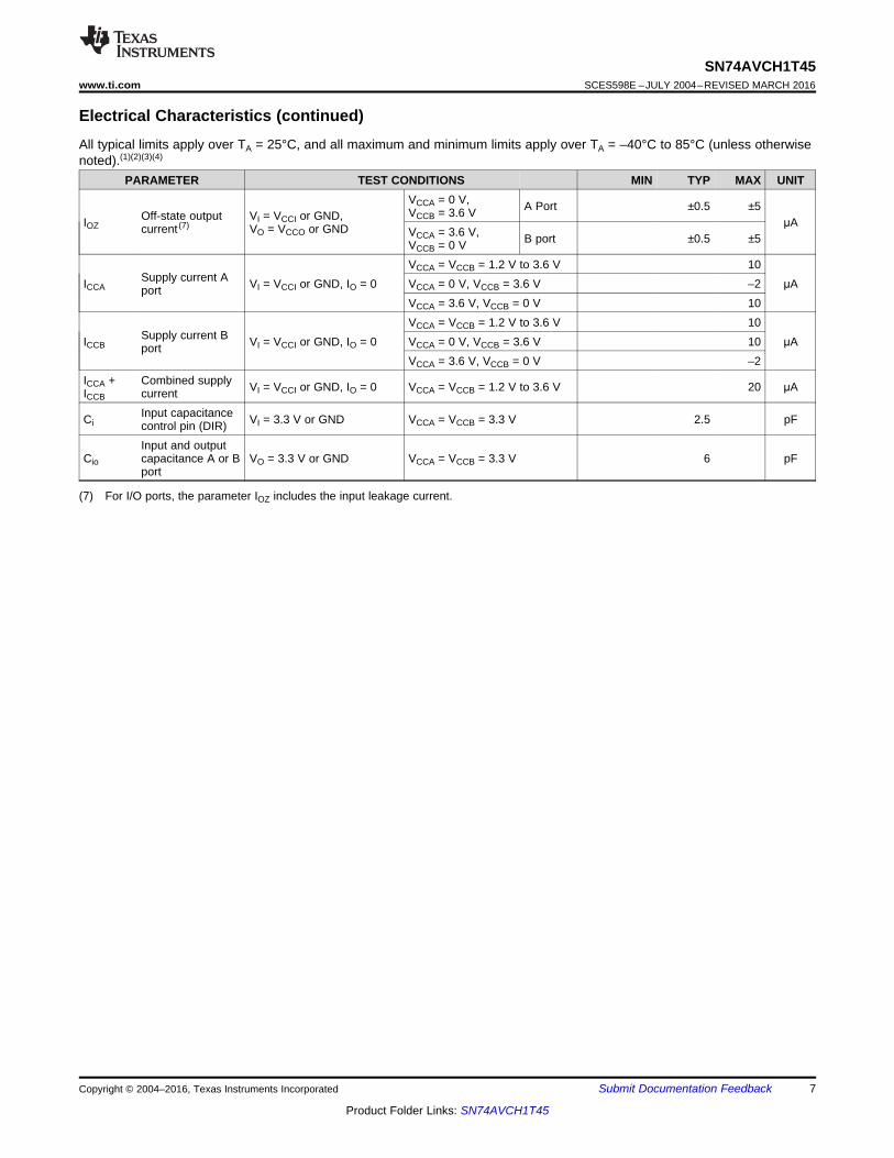
Electrical Characteristics (continued)All typical limits apply over TA = 25°C, and all maximum and minimum limits apply over TA = –40°C to 85°C (unless otherwisenoted).(1)(2)(3)(4)
PARAMETER TEST CONDITIONS MIN TYP MAX UNIT
(7) For I/O ports, the parameter IOZ includes the input leakage current.
IOZOff-state outputcurrent (7)
VI = VCCI or GND,VO = VCCO or GND
VCCA = 0 V,VCCB = 3.6 V A Port ±0.5 ±5
μAVCCA = 3.6 V,VCCB = 0 V B port ±0.5 ±5
ICCASupply current Aport VI = VCCI or GND, IO = 0
VCCA = VCCB = 1.2 V to 3.6 V 10μAVCCA = 0 V, VCCB = 3.6 V –2
VCCA = 3.6 V, VCCB = 0 V 10
ICCBSupply current Bport VI = VCCI or GND, IO = 0
VCCA = VCCB = 1.2 V to 3.6 V 10μAVCCA = 0 V, VCCB = 3.6 V 10
VCCA = 3.6 V, VCCB = 0 V –2ICCA +ICCB
Combined supplycurrent VI = VCCI or GND, IO = 0 VCCA = VCCB = 1.2 V to 3.6 V 20 μA
CiInput capacitancecontrol pin (DIR) VI = 3.3 V or GND VCCA = VCCB = 3.3 V 2.5 pF
Cio
Input and outputcapacitance A or Bport
VO = 3.3 V or GND VCCA = VCCB = 3.3 V 6 pF
8
SN74AVCH1T45SCES598E –JULY 2004–REVISED MARCH 2016 www.ti.com
Product Folder Links: SN74AVCH1T45
Submit Documentation Feedback Copyright © 2004–2016, Texas Instruments Incorporated
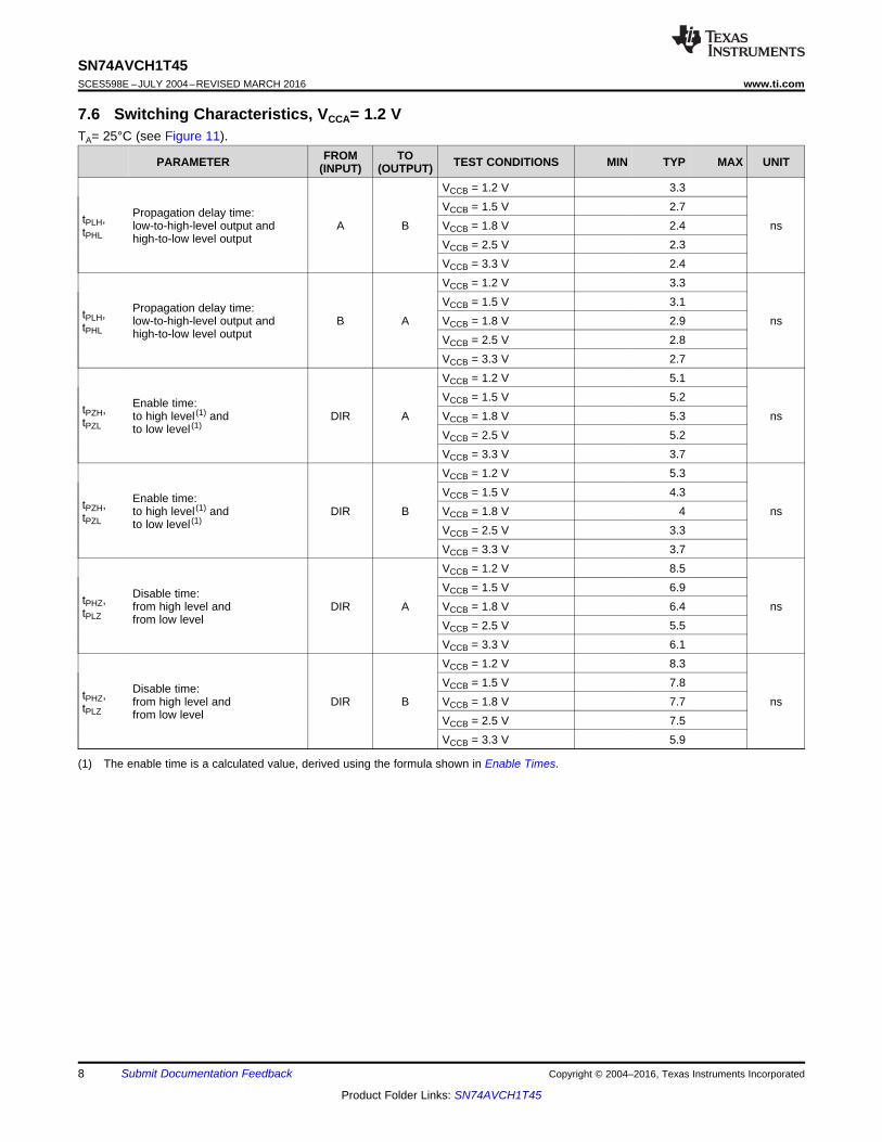
(1) The enable time is a calculated value, derived using the formula shown in Enable Times.
7.6 Switching Characteristics, VCCA= 1.2 VTA= 25°C (see Figure 11).
PARAMETER FROM(INPUT)
TO(OUTPUT) TEST CONDITIONS MIN TYP MAX UNIT
tPLH,tPHL
Propagation delay time:low-to-high-level output andhigh-to-low level output
A B
VCCB = 1.2 V 3.3
nsVCCB = 1.5 V 2.7VCCB = 1.8 V 2.4VCCB = 2.5 V 2.3VCCB = 3.3 V 2.4
tPLH,tPHL
Propagation delay time:low-to-high-level output andhigh-to-low level output
B A
VCCB = 1.2 V 3.3
nsVCCB = 1.5 V 3.1VCCB = 1.8 V 2.9VCCB = 2.5 V 2.8VCCB = 3.3 V 2.7
tPZH,tPZL
Enable time:to high level (1) andto low level (1)
DIR A
VCCB = 1.2 V 5.1
nsVCCB = 1.5 V 5.2VCCB = 1.8 V 5.3VCCB = 2.5 V 5.2VCCB = 3.3 V 3.7
tPZH,tPZL
Enable time:to high level (1) andto low level (1)
DIR B
VCCB = 1.2 V 5.3
nsVCCB = 1.5 V 4.3VCCB = 1.8 V 4VCCB = 2.5 V 3.3VCCB = 3.3 V 3.7
tPHZ,tPLZ
Disable time:from high level andfrom low level
DIR A
VCCB = 1.2 V 8.5
nsVCCB = 1.5 V 6.9VCCB = 1.8 V 6.4VCCB = 2.5 V 5.5VCCB = 3.3 V 6.1
tPHZ,tPLZ
Disable time:from high level andfrom low level
DIR B
VCCB = 1.2 V 8.3
nsVCCB = 1.5 V 7.8VCCB = 1.8 V 7.7VCCB = 2.5 V 7.5VCCB = 3.3 V 5.9

9
SN74AVCH1T45www.ti.com SCES598E –JULY 2004–REVISED MARCH 2016
Product Folder Links: SN74AVCH1T45
Submit Documentation FeedbackCopyright © 2004–2016, Texas Instruments Incorporated
(1) The enable time is a calculated value, derived using the formula shown in Enable Times.
7.7 Switching Characteristics, VCCA= 1.5 V ± 0.1 VAll typical limits apply over TA = 25°C, and all maximum and minimum limits apply over TA = –40°C to 85°C (unless otherwisenoted) (see Figure 11).
PARAMETER FROM(INPUT)
TO(OUTPUT) TEST CONDITIONS MIN TYP MAX UNIT
tPLH,tPHL
Propagation delay time:low-to-high-level output andhigh-to-low level output
A B
VCCB = 1.2 V 2.9
nsVCCB = 1.5 V ± 0.1 V 0.7 5.6VCCB = 1.8 V ± 0.15 V 0.6 4.2VCCB = 2.5 V ± 0.2 V 0.5 4.2VCCB = 3.3 V ± 0.3 V 0.5 3.8
tPLH,tPHL
Propagation delay time:low-to-high-level output andhigh-to-low level output
B A
VCCB = 1.2 V 2.6
nsVCCB = 1.5 V ± 0.1 V 0.6 5.5VCCB = 1.8 V ± 0.15 V 0.4 5.3VCCB = 2.5 V ± 0.2 V 0.3 4.9VCCB = 3.3 V ± 0.3 V 0.3 4.8
tPZH,tPZL
Enable time:to high level (1) andto low level (1)
DIR A
VCCB = 1.2 V 3.8
nsVCCB = 1.5 V ± 0.1 V 1.6 6.7VCCB = 1.8 V ± 0.15 V 1.5 6.8VCCB = 2.5 V ± 0.2 V 0.3 6.9VCCB = 3.3 V ± 0.3 V 0.9 6.9
tPZH,tPZL
Enable time:to high level (1) andto low level (1)
DIR B
VCCB = 1.2 V 5.1
nsVCCB = 1.5 V ± 0.1 V 1.8 8.1VCCB = 1.8 V ± 0.15 V 1.6 7.1VCCB = 2.5 V ± 0.2 V 1.1 4.7VCCB = 3.3 V ± 0.3 V 1.4 4.5
tPHZ,tPLZ
Disable time:from high level andfrom low level
DIR A
VCCB = 1.2 V 7.7
nsVCCB = 1.5 V ± 0.1 V 13.6VCCB = 1.8 V ± 0.15 V 12.4VCCB = 2.5 V ± 0.2 V 9.6VCCB = 3.3 V ± 0.3 V 9.3
tPHZ,tPLZ
Disable time:from high level andfrom low level
DIR B
VCCB = 1.2 V 6.7
nsVCCB = 1.5 V ± 0.1 V 12.3VCCB = 1.8 V ± 0.15 V 12VCCB = 2.5 V ± 0.2 V 11.1VCCB = 3.3 V ± 0.3 V 10.7
10
SN74AVCH1T45SCES598E –JULY 2004–REVISED MARCH 2016 www.ti.com
Product Folder Links: SN74AVCH1T45
Submit Documentation Feedback Copyright © 2004–2016, Texas Instruments Incorporated
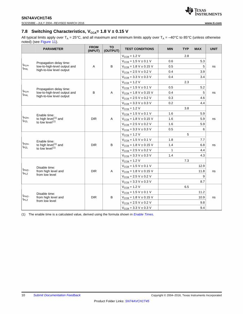
(1) The enable time is a calculated value, derived using the formula shown in Enable Times.
7.8 Switching Characteristics, VCCA= 1.8 V ± 0.15 VAll typical limits apply over TA = 25°C, and all maximum and minimum limits apply over TA = –40°C to 85°C (unless otherwisenoted) (see Figure 11).
PARAMETER FROM(INPUT)
TO(OUTPUT) TEST CONDITIONS MIN TYP MAX UNIT
tPLH,tPHL
Propagation delay time:low-to-high-level output andhigh-to-low level output
A B
VCCB = 1.2 V 2.8
nsVCCB = 1.5 V ± 0.1 V 0.6 5.3VCCB = 1.8 V ± 0.15 V 0.5 5VCCB = 2.5 V ± 0.2 V 0.4 3.9VCCB = 3.3 V ± 0.3 V 0.4 3.4
tPLH,tPHL
Propagation delay time:low-to-high-level output andhigh-to-low level output
B A
VCCB = 1.2 V 2.3
nsVCCB = 1.5 V ± 0.1 V 0.5 5.2VCCB = 1.8 V ± 0.15 V 0.4 5VCCB = 2.5 V ± 0.2 V 0.3 4.6VCCB = 3.3 V ± 0.3 V 0.2 4.4
tPZH,tPZL
Enable time:to high level (1) andto low level (1)
DIR A
VCCB = 1.2 V 3.8
nsVCCB = 1.5 V ± 0.1 V 1.6 5.9VCCB = 1.8 V ± 0.15 V 1.6 5.9VCCB = 2.5 V ± 0.2 V 1.6 5.9VCCB = 3.3 V ± 0.3 V 0.5 6
tPZH,tPZL
Enable time:to high level (1) andto low level (1)
DIR B
VCCB = 1.2 V 5
nsVCCB = 1.5 V ± 0.1 V 1.8 7.7VCCB = 1.8 V ± 0.15 V 1.4 6.8VCCB = 2.5 V ± 0.2 V 1 4.4VCCB = 3.3 V ± 0.3 V 1.4 4.3
tPHZ,tPLZ
Disable time:from high level andfrom low level
DIR A
VCCB = 1.2 V 7.3
nsVCCB = 1.5 V ± 0.1 V 12.9VCCB = 1.8 V ± 0.15 V 11.8VCCB = 2.5 V ± 0.2 V 9VCCB = 3.3 V ± 0.3 V 8.7
tPHZ,tPLZ
Disable time:from high level andfrom low level
DIR B
VCCB = 1.2 V 6.5
nsVCCB = 1.5 V ± 0.1 V 11.2VCCB = 1.8 V ± 0.15 V 10.9VCCB = 2.5 V ± 0.2 V 9.8VCCB = 3.3 V ± 0.3 V 9.4
11
SN74AVCH1T45www.ti.com SCES598E –JULY 2004–REVISED MARCH 2016
Product Folder Links: SN74AVCH1T45
Submit Documentation FeedbackCopyright © 2004–2016, Texas Instruments Incorporated
(1) The enable time is a calculated value, derived using the formula shown in Enable Times.
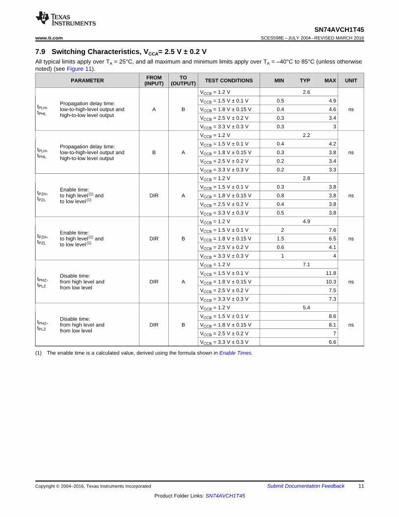
7.9 Switching Characteristics, VCCA= 2.5 V ± 0.2 VAll typical limits apply over TA = 25°C, and all maximum and minimum limits apply over TA = –40°C to 85°C (unless otherwisenoted) (see Figure 11).
PARAMETER FROM(INPUT)
TO(OUTPUT) TEST CONDITIONS MIN TYP MAX UNIT
tPLH,tPHL
Propagation delay time:low-to-high-level output andhigh-to-low level output
A B
VCCB = 1.2 V 2.6
nsVCCB = 1.5 V ± 0.1 V 0.5 4.9VCCB = 1.8 V ± 0.15 V 0.4 4.6VCCB = 2.5 V ± 0.2 V 0.3 3.4VCCB = 3.3 V ± 0.3 V 0.3 3
tPLH,tPHL
Propagation delay time:low-to-high-level output andhigh-to-low level output
B A
VCCB = 1.2 V 2.2
nsVCCB = 1.5 V ± 0.1 V 0.4 4.2VCCB = 1.8 V ± 0.15 V 0.3 3.8VCCB = 2.5 V ± 0.2 V 0.2 3.4VCCB = 3.3 V ± 0.3 V 0.2 3.3
tPZH,tPZL
Enable time:to high level (1) andto low level (1)
DIR A
VCCB = 1.2 V 2.8
nsVCCB = 1.5 V ± 0.1 V 0.3 3.8VCCB = 1.8 V ± 0.15 V 0.8 3.8VCCB = 2.5 V ± 0.2 V 0.4 3.8VCCB = 3.3 V ± 0.3 V 0.5 3.8
tPZH,tPZL
Enable time:to high level (1) andto low level (1)
DIR B
VCCB = 1.2 V 4.9
nsVCCB = 1.5 V ± 0.1 V 2 7.6VCCB = 1.8 V ± 0.15 V 1.5 6.5VCCB = 2.5 V ± 0.2 V 0.6 4.1VCCB = 3.3 V ± 0.3 V 1 4
tPHZ,tPLZ
Disable time:from high level andfrom low level
DIR A
VCCB = 1.2 V 7.1
nsVCCB = 1.5 V ± 0.1 V 11.8VCCB = 1.8 V ± 0.15 V 10.3VCCB = 2.5 V ± 0.2 V 7.5VCCB = 3.3 V ± 0.3 V 7.3
tPHZ,tPLZ
Disable time:from high level andfrom low level
DIR B
VCCB = 1.2 V 5.4
nsVCCB = 1.5 V ± 0.1 V 8.6VCCB = 1.8 V ± 0.15 V 8.1VCCB = 2.5 V ± 0.2 V 7VCCB = 3.3 V ± 0.3 V 6.6

12
SN74AVCH1T45SCES598E –JULY 2004–REVISED MARCH 2016 www.ti.com
Product Folder Links: SN74AVCH1T45
Submit Documentation Feedback Copyright © 2004–2016, Texas Instruments Incorporated
(1) The enable time is a calculated value, derived using the formula shown in Enable Times.
7.10 Switching Characteristics, VCCA= 3.3 V ± 0.3 VAll typical limits apply over TA = 25°C, and all maximum and minimum limits apply over TA = –40°C to 85°C (unless otherwisenoted) (see Figure 11).
PARAMETER FROM(INPUT)
TO(OUTPUT) TEST CONDITIONS MIN TYP MAX UNIT
tPLH,tPHL
Propagation delay time:low-to-high-level output andhigh-to-low level output
A B
VCCB = 1.2 V 2.6
nsVCCB = 1.5 V ± 0.1 V 0.4 4.7VCCB = 1.8 V ± 0.15 V 0.3 4.4VCCB = 2.5 V ± 0.2 V 0.2 3.3VCCB = 3.3 V ± 0.3 V 0.2 2.8
tPLH,tPHL
Propagation delay time:low-to-high-level output andhigh-to-low level output
B A
VCCB = 1.2 V 2.2
nsVCCB = 1.5 V ± 0.1 V 0.4 3.8VCCB = 1.8 V ± 0.15 V 0.3 3.4VCCB = 2.5 V ± 0.2 V 0.2 3VCCB = 3.3 V ± 0.3 V 0.1 2.8
tPZH,tPZL
Enable time:to high level (1) andto low level (1)
DIR A
VCCB = 1.2 V 3.1
nsVCCB = 1.5 V ± 0.1 V 1.3 4.3VCCB = 1.8 V ± 0.15 V 1.3 4.3VCCB = 2.5 V ± 0.2 V 1.3 4.3VCCB = 3.3 V ± 0.3 V 1.3 4.3
tPZH,tPZL
Enable time:to high level (1) andto low level (1)
DIR B
VCCB = 1.2 V 4
nsVCCB = 1.5 V ± 0.1 V 0.7 7.4VCCB = 1.8 V ± 0.15 V 0.6 6.5VCCB = 2.5 V ± 0.2 V 0.7 4VCCB = 3.3 V ± 0.3 V 1.5 3.9
tPHZ,tPLZ
Disable time:from high level andfrom low level
DIR A
VCCB = 1.2 V 6.2
nsVCCB = 1.5 V ± 0.1 V 11.2VCCB = 1.8 V ± 0.15 V 9.9VCCB = 2.5 V ± 0.2 V 7VCCB = 3.3 V ± 0.3 V 6.7
tPHZ,tPLZ
Disable time:from high level andfrom low level
DIR B
VCCB = 1.2 V 5.7
nsVCCB = 1.5 V ± 0.1 V 8.9VCCB = 1.8 V ± 0.15 V 8.5VCCB = 2.5 V ± 0.2 V 7.2VCCB = 3.3 V ± 0.3 V 6.8
13
SN74AVCH1T45www.ti.com SCES598E –JULY 2004–REVISED MARCH 2016
Product Folder Links: SN74AVCH1T45
Submit Documentation FeedbackCopyright © 2004–2016, Texas Instruments Incorporated
(1) See CMOS Power Consumption and Cpd Calculation, SCAA035.
7.11 Operating CharacteristicsTA= 25°C
PARAMETER FROM(INPUT)
TO(OUTPUT) TEST CONDITIONS TYP UNIT
CpdA
Power dissipation capacitanceper transceiver (1)
port A
A BCL = 0 pF,f = 10 MHz,tr = tf = 1 ns
VCCA = VCCB = 1.2 V 3
pFVCCA = VCCB = 1.5 V 3VCCA = VCCB = 1.8 V 3VCCA = VCCB = 2.5 V 3VCCA = VCCB = 3.3 V 4
B ACL = 0 pF,f = 10 MHz,tr = tf = 1 ns
VCCA = VCCB = 1.2 V 14
pFVCCA = VCCB = 1.5 V 14VCCA = VCCB = 1.8 V 14VCCA = VCCB = 2.5 V 15VCCA = VCCB = 3.3 V 16
CpdB
Power dissipation capacitanceper transceiver (1)
port B
A BCL = 0 pF,f = 10 MHz,tr = tf = 1 ns
VCCA = VCCB = 1.2 V 14
pFVCCA = VCCB = 1.5 V 14VCCA = VCCB = 1.8 V 14VCCA = VCCB = 2.5 V 15VCCA = VCCB = 3.3 V 16
B ACL = 0 pF,f = 10 MHz,tr = tf = 1 ns
VCCA = VCCB = 1.2 V 3
pFVCCA = VCCB = 1.5 V 3VCCA = VCCB = 1.8 V 3VCCA = VCCB = 2.5 V 3VCCA = VCCB = 3.3 V 4
0
1
2
3
4
5
6
0 10 20 30 40 50
t PLH
- n
s
CL - pF
60
VCCB = 1.8 V
VCCB = 2.5 V
VCCB = 3.3 V
VCCB = 1.5 V
VCCB = 1.2 V
t PH
L - n
s
CL - pF
0
1
2
3
4
5
6
0 10 20 30 40 50 60
VCCB = 1.8 V
VCCB = 2.5 V
VCCB = 3.3 V
VCCB = 1.5 V
VCCB = 1.2 V
0
1
2
3
4
5
6
0 10 20 30 40 50
t PLH
- n
s
CL - pF
60
VCCB = 1.8 V
VCCB = 2.5 V
VCCB = 3.3 V
VCCB = 1.5 V
VCCB = 1.2 V
t PH
L - n
s
CL - pF
0
1
2
3
4
5
6
0 10 20 30 40 50 60
VCCB = 1.8 V
VCCB = 2.5 V
VCCB = 3.3 V
VCCB = 1.5 V
VCCB = 1.2 V
0
1
2
3
4
5
6
0 10 20 30 40 50
t PLH
- n
s
CL - pF
60
VCCB = 1.8 V
VCCB = 2.5 V
VCCB = 3.3 V
VCCB = 1.5 V
VCCB = 1.2 V
t PH
L - n
s
CL - pF
0
1
2
3
4
5
6
0 10 20 30 40 50 60
VCCB = 1.8 V
VCCB = 2.5 V
VCCB = 3.3 V
VCCB = 1.5 V
VCCB = 1.2 V
14
SN74AVCH1T45SCES598E –JULY 2004–REVISED MARCH 2016 www.ti.com
Product Folder Links: SN74AVCH1T45
Submit Documentation Feedback Copyright © 2004–2016, Texas Instruments Incorporated
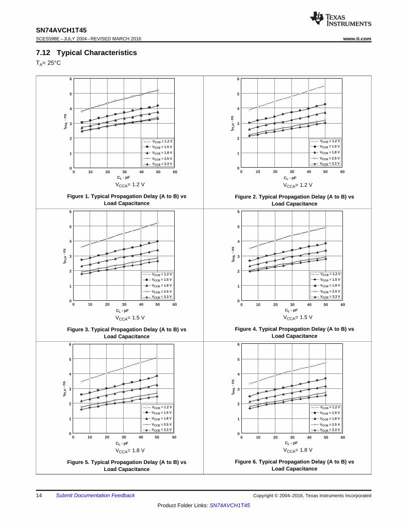
7.12 Typical CharacteristicsTA= 25°C
VCCA= 1.2 V
Figure 1. Typical Propagation Delay (A to B) vsLoad Capacitance
VCCA= 1.2 V
Figure 2. Typical Propagation Delay (A to B) vsLoad Capacitance
VCCA= 1.5 V
Figure 3. Typical Propagation Delay (A to B) vsLoad Capacitance
VCCA= 1.5 V
Figure 4. Typical Propagation Delay (A to B) vsLoad Capacitance
VCCA= 1.8 V
Figure 5. Typical Propagation Delay (A to B) vsLoad Capacitance
VCCA= 1.8 V
Figure 6. Typical Propagation Delay (A to B) vsLoad Capacitance

0
1
2
3
4
5
6
0 10 20 30 40 50
t PLH
- n
s
CL - pF
60
VCCB = 1.8 V
VCCB = 2.5 V
VCCB = 3.3 V
VCCB = 1.5 V
VCCB = 1.2 V
t PH
L - n
s
CL - pF
0
1
2
3
4
5
6
0 10 20 30 40 50 60
VCCB = 1.8 V
VCCB = 2.5 V
VCCB = 3.3 V
VCCB = 1.5 V
VCCB = 1.2 V
0
1
2
3
4
5
6
0 10 20 30 40 50
t PLH
- n
s
CL - pF
60
VCCB = 1.8 V
VCCB = 2.5 V
VCCB = 3.3 V
VCCB = 1.5 V
VCCB = 1.2 V
t PH
L - n
s
CL - pF
0
1
2
3
4
5
6
0 10 20 30 40 50 60
VCCB = 1.8 V
VCCB = 2.5 V
VCCB = 3.3 V
VCCB = 1.5 V
VCCB = 1.2 V
15
SN74AVCH1T45www.ti.com SCES598E –JULY 2004–REVISED MARCH 2016
Product Folder Links: SN74AVCH1T45
Submit Documentation FeedbackCopyright © 2004–2016, Texas Instruments Incorporated
Typical Characteristics (continued)TA= 25°C
VCCA= 2.5 V
Figure 7. Typical Propagation Delay (A to B) vsLoad Capacitance
VCCA= 2.5 V
Figure 8. Typical Propagation Delay (A to B) vsLoad Capacitance
VCCA= 3.3 V
Figure 9. Typical Propagation Delay (A to B) vsLoad Capacitance
VCCA= 3.3 V
Figure 10. Typical Propagation Delay (A to B) vsLoad Capacitance
VOH
VOL
From Output
Under Test
CL
(see Note A)
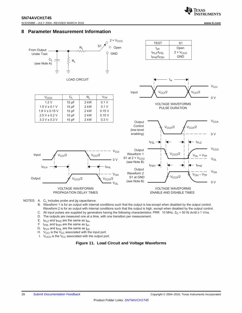
LOAD CIRCUIT
S1
2 × VCCO
Open
GND
RL
RL
tPLH tPHL
Output
Control
(low-level
enabling)
Output
Waveform 1
S1 at 2 × VCCO
(see Note B)
Output
Waveform 2
S1 at GND
(see Note B)
tPZL
tPZH
tPLZ
tPHZ
VCCA/2VCCA/2
VCCI/2 VCCI/2
VCCI
0 V
VCCO/2 VCCO/2
VOH
VOL
0 V
VCCO/2VOL + VTP
VCCO/2VOH – VTP
0 V
VCCI
0 V
VCCI/2 VCCI/2
tw
Input
VCCA
VCCO
VOLTAGE WAVEFORMS
PROPAGATION DELAY TIMES
VOLTAGE WAVEFORMS
PULSE DURATION
VOLTAGE WAVEFORMS
ENABLE AND DISABLE TIMES
Output
Input
tpd
tPLZ/tPZL
tPHZ/tPZH
Open
2 × VCCO
GND
TEST S1
NOTES: A. CL includes probe and jig capacitance.
B. Waveform 1 is for an output with internal conditions such that the output is low, except when disabled by the output control.
Waveform 2 is for an output with internal conditions such that the output is high, except when disabled by the output control.
C. All input pulses are supplied by generators having the following characteristics: PRR 10 MHz, ZO = 50 W, dv/dt ≥ 1 V/ns.
D. The outputs are measured one at a time, with one transition per measurement.
E. tPLZ and tPHZ are the same as tdis.
F. tPZL and tPZH are the same as ten.
G. tPLH and tPHL are the same as tpd.
H. VCCI is the VCC associated with the input port.
I. VCCO is the VCC associated with the output port.
1.2 V
1.5 V ± 0.1 V
1.8 V ± 0.15 V
2.5 V ± 0.2 V
3.3 V ± 0.3 V
2 kW
2 kW
2 kW
2 kW
2 kW
VCCO RL
0.1 V
0.1 V
0.15 V
0.15 V
0.3 V
VTPCL
15 pF
15 pF
15 pF
15 pF
15 pF
16
SN74AVCH1T45SCES598E –JULY 2004–REVISED MARCH 2016 www.ti.com
Product Folder Links: SN74AVCH1T45
Submit Documentation Feedback Copyright © 2004–2016, Texas Instruments Incorporated
8 Parameter Measurement Information
Figure 11. Load Circuit and Voltage Waveforms
B
DIR5
4
A3
VCCA VCCB
17
SN74AVCH1T45www.ti.com SCES598E –JULY 2004–REVISED MARCH 2016
Product Folder Links: SN74AVCH1T45
Submit Documentation FeedbackCopyright © 2004–2016, Texas Instruments Incorporated
9 Detailed Description
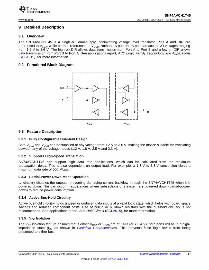
9.1 OverviewThe SN74AVCH1T45 is a single-bit, dual-supply, noninverting voltage level translator. Pins A and DIR arereferenced to VCCA, while pin B is referenced to VCCB. Both the A port and B port can accept I/O voltages rangingfrom 1.2 V to 3.6 V. The high on DIR allows data transmission from Port A to Port B and a low on DIR allowsdata transmission from Port B to Port A. See applications report, AVC Logic Family Technology and Applications(SCLA015), for more information.
9.2 Functional Block Diagram
9.3 Feature Description
9.3.1 Fully Configurable Dual-Rail DesignBoth VCCA and VCCB can be supplied at any voltage from 1.2 V to 3.6 V, making the device suitable for translatingbetween any of the voltage nodes (1.2 V, 1.8 V, 2.5 V and 3.3 V).
9.3.2 Supports High-Speed TranslationSN74AVCH1T45 can support high data rate applications, which can be calculated from the maximumpropagation delay. This is also dependent on output load. For example, a 1.8-V to 3.3-V conversion yields amaximum data rate of 500 Mbps.
9.3.3 Partial-Power-Down Mode OperationIoff circuitry disables the outputs, preventing damaging current backflow through the SN74AVCH1T45 when it ispowered down. This can occur in applications where subsections of a system are powered down (partial-power-down) to reduce power consumption.
9.3.4 Active Bus-Hold CircuitryActive bus-hold circuitry holds unused or undriven data inputs at a valid logic state, which helps with board spacesavings and reduced component costs. Use of pullup or pulldown resistors with the bus-hold circuitry is notrecommended. See applications report, Bus-Hold Circuit (SCLA015), for more information.
9.3.5 VCC IsolationThe VCC isolation feature ensures that if either VCCA or VCCB are at GND (or < 0.4 V), both ports will be in a high-impedance state (IOZ as shown in Electrical Characteristics). This prevents false logic levels from beingpresented to either bus.
1
2
3
6
5
4
VCC1 VCC1 VCC2 VCC2
SYSTEM-1 SYSTEM-2
18
SN74AVCH1T45SCES598E –JULY 2004–REVISED MARCH 2016 www.ti.com
Product Folder Links: SN74AVCH1T45
Submit Documentation Feedback Copyright © 2004–2016, Texas Instruments Incorporated
9.4 Device Functional ModesTable 1 lists the functional modes of the SN74AVCH1T45.
Table 1. Function TableDIR OPERATION
L B data to A busH A data to B bus
10 Application and Implementation
NOTEInformation in the following applications sections is not part of the TI componentspecification, and TI does not warrant its accuracy or completeness. TI’s customers areresponsible for determining suitability of components for their purposes. Customers shouldvalidate and test their design implementation to confirm system functionality.
10.1 Application InformationThe SN74AVCH1T45 device can be used in level-translation applications for interfacing devices or systemsoperating at different interface voltages with one another. The maximum data rate can be up to 500 Mbps whendevice translate signal from 1.8 V to 3.3 V.
10.2 Typical Applications
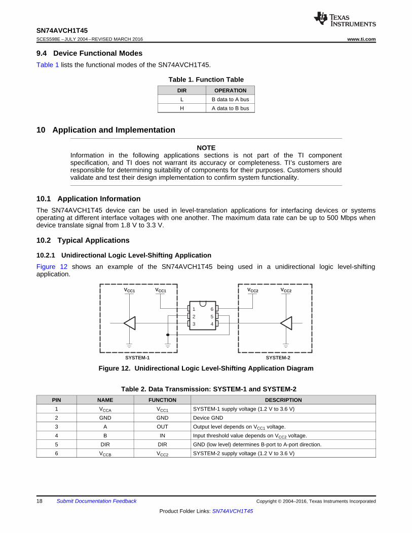
10.2.1 Unidirectional Logic Level-Shifting ApplicationFigure 12 shows an example of the SN74AVCH1T45 being used in a unidirectional logic level-shiftingapplication.
Figure 12. Unidirectional Logic Level-Shifting Application Diagram
Table 2. Data Transmission: SYSTEM-1 and SYSTEM-2PIN NAME FUNCTION DESCRIPTION
1 VCCA VCC1 SYSTEM-1 supply voltage (1.2 V to 3.6 V)2 GND GND Device GND3 A OUT Output level depends on VCC1 voltage.4 B IN Input threshold value depends on VCC2 voltage.5 DIR DIR GND (low level) determines B-port to A-port direction.6 VCCB VCC2 SYSTEM-2 supply voltage (1.2 V to 3.6 V)

19
SN74AVCH1T45www.ti.com SCES598E –JULY 2004–REVISED MARCH 2016
Product Folder Links: SN74AVCH1T45
Submit Documentation FeedbackCopyright © 2004–2016, Texas Instruments Incorporated
10.2.1.1 Design RequirementsFor this design example, use the parameters listed in Table 3.
Table 3. Design ParametersDESIGN PARAMETERS EXAMPLE VALUES
Input voltage 1.2 V to 3.6 VOutput voltage 1.2 V to 3.6 V
10.2.1.2 Detailed Design ProcedureTo begin the design process, determine the following:• Input voltage range
– Use the supply voltage of the device that is driving the SN74AVCH1T45 device to determine the inputvoltage range. For a valid logic-high, the value must exceed the VIH of the input port. For a valid logic lowthe value must be less than the VIL of the input port.
• Output voltage range– Use the supply voltage of the device that the SN74AVCH1T45 device is driving to determine the output
voltage range.
10.2.1.3 Application Curve
Figure 13. Translation Up (1.2 V to 3.3 V) at 2.5 MHz

1
2
3
6
5
4
VCC1 VCC1 VCC2
SYSTEM-1 SYSTEM-2
DIR CTRL
I/O-1 I/O-2
VCC2
20
SN74AVCH1T45SCES598E –JULY 2004–REVISED MARCH 2016 www.ti.com
Product Folder Links: SN74AVCH1T45
Submit Documentation Feedback Copyright © 2004–2016, Texas Instruments Incorporated
10.2.2 Bidirectional Logic Level-Shifting ApplicationFigure 14 shows the SN74AVCH1T45 being used in a bidirectional logic level-shifting application. Because theSN74AVCH1T45 does not have an output-enable (OE) pin, the system designer should take precautions to avoidbus contention between SYSTEM-1 and SYSTEM-2 when changing directions.
Figure 14. Bidirectional Logic Level-Shifting Application Diagram
The following table shows data transmission from SYSTEM-1 to SYSTEM-2 and then from SYSTEM-2 toSYSTEM-1.
Table 4. Data Transmission: SYSTEM-1 and SYSTEM-2STATE DIR CTRL I/O-1 I/O-2 DESCRIPTION
1 H Out In SYSTEM-1 data to SYSTEM-22 H Hi-Z Hi-Z SYSTEM-2 is getting ready to send data to SYSTEM-1. I/O-1 and I/O-2 are disabled.3 L Hi-Z Hi-Z DIR bit is flipped. I/O-1 and I/O-2 still are disabled.4 L In Out SYSTEM-2 data to SYSTEM-1
10.2.2.1 Design RequirementsRefer to Design Requirements found in Unidirectional Logic Level-Shifting Application.
10.2.2.2 Detailed Design Procedure
10.2.2.2.1 Enable Times
Calculate the enable times for the SN74AVCH1T45 using the following formulas:• tPZH (DIR to A) = tPLZ(DIR to B) + tPLH (B to A)• tPZL (DIR to A) = tPHZ(DIR to B) + tPHL (B to A)• tPZH (DIR to B) = tPLZ(DIR to A) + tPLH (A to B)• tPZL (DIR to B) = tPHZ(DIR to A) + tPHL (A to B)
In a bidirectional application, these enable times provide the maximum delay from the time the DIR bit isswitched until an output is expected. For example, if the SN74AVCH1T45 initially is transmitting from A to B, thenthe DIR bit is switched; the B port of the device must be disabled before presenting it with an input. After the Bport has been disabled, an input signal applied to it appears on the corresponding A port after the specifiedpropagation delay.

21
SN74AVCH1T45www.ti.com SCES598E –JULY 2004–REVISED MARCH 2016
Product Folder Links: SN74AVCH1T45
Submit Documentation FeedbackCopyright © 2004–2016, Texas Instruments Incorporated
10.2.2.3 Application Curve
Figure 15. Translation Up (1.2 V to 3.3 V) at 2.5 MHz
11 Power Supply Recommendations
A proper power-up sequence must be followed to avoid excessive supply current, bus contention, oscillations, orother anomalies. To guard against such power-up problems, take the following precautions:1. Connect ground before any supply voltage is applied.2. Power up VCCA.3. VCCB can be ramped up along with or after VCCA.
Table 5. Typical Total Static Power Consumption (ICCA + ICCB)
VCCBVCCA UNIT
0 V 1.2 V 1.5 V 1.8 V 2.5 V 3.3 V0 V 0 <0.5 <0.5 <0.5 <0.5 <0.5
μA
1.2 V <0.5 <1 <1 <1 <1 11.5 V <0.5 <1 <1 <1 <1 11.8 V <0.5 <1 <1 <1 <1 <12.5 V <0.5 1 <1 <1 <1 <13.3 V <0.5 1 <1 <1 <1 <1
22
SN74AVCH1T45SCES598E –JULY 2004–REVISED MARCH 2016 www.ti.com
Product Folder Links: SN74AVCH1T45
Submit Documentation Feedback Copyright © 2004–2016, Texas Instruments Incorporated
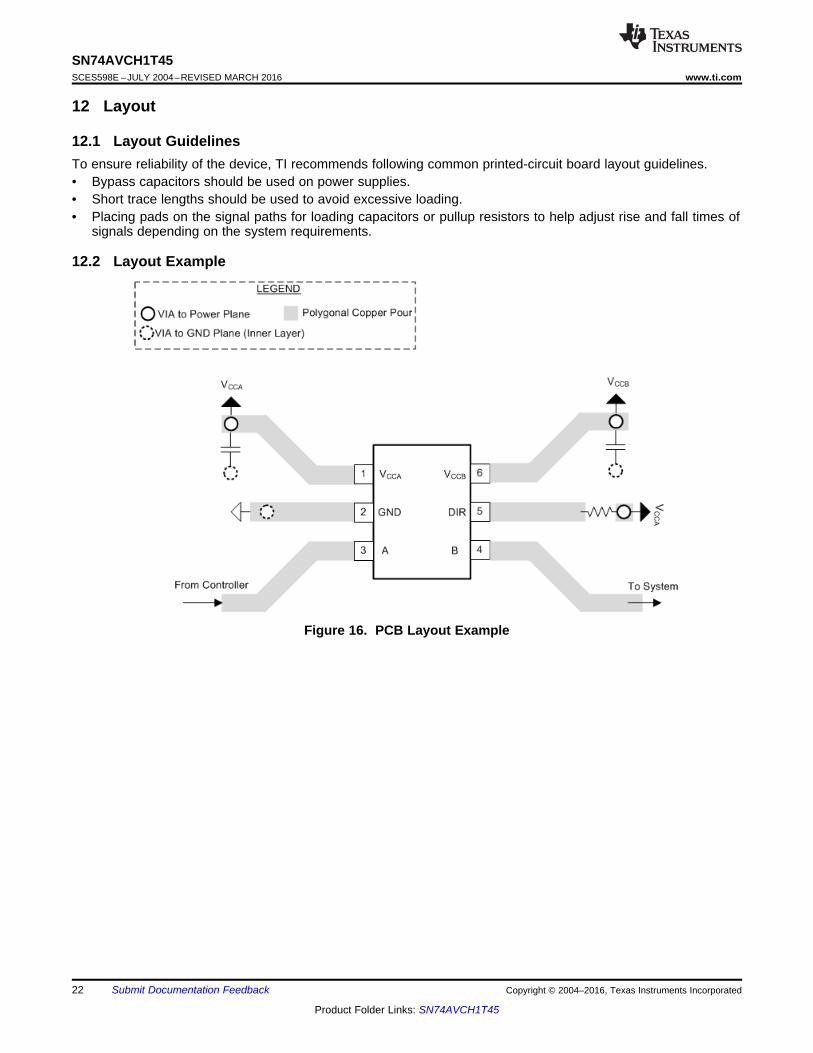
12 Layout
12.1 Layout GuidelinesTo ensure reliability of the device, TI recommends following common printed-circuit board layout guidelines.• Bypass capacitors should be used on power supplies.• Short trace lengths should be used to avoid excessive loading.• Placing pads on the signal paths for loading capacitors or pullup resistors to help adjust rise and fall times of
signals depending on the system requirements.
12.2 Layout Example
Figure 16. PCB Layout Example
23
SN74AVCH1T45www.ti.com SCES598E –JULY 2004–REVISED MARCH 2016
Product Folder Links: SN74AVCH1T45
Submit Documentation FeedbackCopyright © 2004–2016, Texas Instruments Incorporated
13 Device and Documentation Support
13.1 Documentation Support
13.1.1 Related DocumentationFor related documentation see the following:• Designing with SN74LVCXT245 and SN74LVCHXT245 Family of Direction Controlled Voltage
Translators/Level-Shifters, SLVA746• Bus-Hold Circuit, SCLA015• AVC Logic Family Technology and Applications, SCEA006
13.2 Community ResourcesThe following links connect to TI community resources. Linked contents are provided "AS IS" by the respectivecontributors. They do not constitute TI specifications and do not necessarily reflect TI's views; see TI's Terms ofUse.
TI E2E™ Online Community TI's Engineer-to-Engineer (E2E) Community. Created to foster collaborationamong engineers. At e2e.ti.com, you can ask questions, share knowledge, explore ideas and helpsolve problems with fellow engineers.
Design Support TI's Design Support Quickly find helpful E2E forums along with design support tools andcontact information for technical support.
13.3 TrademarksNanoStar, NanoFree, E2E are trademarks of Texas Instruments.All other trademarks are the property of their respective owners.
13.4 Electrostatic Discharge CautionThese devices have limited built-in ESD protection. The leads should be shorted together or the device placed in conductive foamduring storage or handling to prevent electrostatic damage to the MOS gates.
13.5 GlossarySLYZ022 — TI Glossary.
This glossary lists and explains terms, acronyms, and definitions.
14 Mechanical, Packaging, and Orderable InformationThe following pages include mechanical, packaging, and orderable information. This information is the mostcurrent data available for the designated devices. This data is subject to change without notice and revision ofthis document. For browser-based versions of this data sheet, refer to the left-hand navigation.

PACKAGE OPTION ADDENDUM
www.ti.com 25-Oct-2016
Addendum-Page 1
PACKAGING INFORMATION
Orderable Device Status(1)
Package Type PackageDrawing
Pins PackageQty
Eco Plan(2)
Lead/Ball Finish(6)
MSL Peak Temp(3)
Op Temp (°C) Device Marking(4/5)
Samples
74AVCH1T45DBVRE4 ACTIVE SOT-23 DBV 6 3000 Green (RoHS& no Sb/Br)
CU NIPDAU Level-1-260C-UNLIM -40 to 85 (ET1F ~ ET1R)
74AVCH1T45DBVRG4 ACTIVE SOT-23 DBV 6 3000 Green (RoHS& no Sb/Br)
CU NIPDAU Level-1-260C-UNLIM -40 to 85 (ET1F ~ ET1R)
74AVCH1T45DBVTG4 ACTIVE SOT-23 DBV 6 250 Green (RoHS& no Sb/Br)
CU NIPDAU Level-1-260C-UNLIM -40 to 85 (ET1F ~ ET1R)
74AVCH1T45DCKRE4 ACTIVE SC70 DCK 6 3000 Green (RoHS& no Sb/Br)
CU NIPDAU Level-1-260C-UNLIM -40 to 85 (TFF ~ TFR)
74AVCH1T45DCKRG4 ACTIVE SC70 DCK 6 3000 Green (RoHS& no Sb/Br)
CU NIPDAU Level-1-260C-UNLIM -40 to 85 (TFF ~ TFR)
74AVCH1T45DCKTG4 ACTIVE SC70 DCK 6 250 Green (RoHS& no Sb/Br)
CU NIPDAU Level-1-260C-UNLIM -40 to 85 (TFF ~ TFR)
SN74AVCH1T45DBVR ACTIVE SOT-23 DBV 6 3000 Green (RoHS& no Sb/Br)
CU NIPDAU Level-1-260C-UNLIM -40 to 85 (ET1F ~ ET1R)
SN74AVCH1T45DBVT ACTIVE SOT-23 DBV 6 250 Green (RoHS& no Sb/Br)
CU NIPDAU Level-1-260C-UNLIM -40 to 85 (ET1F ~ ET1R)
SN74AVCH1T45DCKR ACTIVE SC70 DCK 6 3000 Green (RoHS& no Sb/Br)
CU NIPDAU Level-1-260C-UNLIM -40 to 85 (TFF ~ TFR)
SN74AVCH1T45DCKT ACTIVE SC70 DCK 6 250 Green (RoHS& no Sb/Br)
CU NIPDAU Level-1-260C-UNLIM -40 to 85 (TFF ~ TFR)
SN74AVCH1T45YZPR ACTIVE DSBGA YZP 6 3000 Green (RoHS& no Sb/Br)
SNAGCU Level-1-260C-UNLIM -40 to 85 (TE2 ~ TE7 ~ TEN)
(1) The marketing status values are defined as follows:ACTIVE: Product device recommended for new designs.LIFEBUY: TI has announced that the device will be discontinued, and a lifetime-buy period is in effect.NRND: Not recommended for new designs. Device is in production to support existing customers, but TI does not recommend using this part in a new design.PREVIEW: Device has been announced but is not in production. Samples may or may not be available.OBSOLETE: TI has discontinued the production of the device.
(2) Eco Plan - The planned eco-friendly classification: Pb-Free (RoHS), Pb-Free (RoHS Exempt), or Green (RoHS & no Sb/Br) - please check http://www.ti.com/productcontent for the latest availabilityinformation and additional product content details.TBD: The Pb-Free/Green conversion plan has not been defined.Pb-Free (RoHS): TI's terms "Lead-Free" or "Pb-Free" mean semiconductor products that are compatible with the current RoHS requirements for all 6 substances, including the requirement thatlead not exceed 0.1% by weight in homogeneous materials. Where designed to be soldered at high temperatures, TI Pb-Free products are suitable for use in specified lead-free processes.
PACKAGE OPTION ADDENDUM
www.ti.com 25-Oct-2016
Addendum-Page 2
Pb-Free (RoHS Exempt): This component has a RoHS exemption for either 1) lead-based flip-chip solder bumps used between the die and package, or 2) lead-based die adhesive used betweenthe die and leadframe. The component is otherwise considered Pb-Free (RoHS compatible) as defined above.Green (RoHS & no Sb/Br): TI defines "Green" to mean Pb-Free (RoHS compatible), and free of Bromine (Br) and Antimony (Sb) based flame retardants (Br or Sb do not exceed 0.1% by weightin homogeneous material)
(3) MSL, Peak Temp. - The Moisture Sensitivity Level rating according to the JEDEC industry standard classifications, and peak solder temperature.
(4) There may be additional marking, which relates to the logo, the lot trace code information, or the environmental category on the device.
(5) Multiple Device Markings will be inside parentheses. Only one Device Marking contained in parentheses and separated by a "~" will appear on a device. If a line is indented then it is a continuationof the previous line and the two combined represent the entire Device Marking for that device.
(6) Lead/Ball Finish - Orderable Devices may have multiple material finish options. Finish options are separated by a vertical ruled line. Lead/Ball Finish values may wrap to two lines if the finishvalue exceeds the maximum column width.
Important Information and Disclaimer:The information provided on this page represents TI's knowledge and belief as of the date that it is provided. TI bases its knowledge and belief on informationprovided by third parties, and makes no representation or warranty as to the accuracy of such information. Efforts are underway to better integrate information from third parties. TI has taken andcontinues to take reasonable steps to provide representative and accurate information but may not have conducted destructive testing or chemical analysis on incoming materials and chemicals.TI and TI suppliers consider certain information to be proprietary, and thus CAS numbers and other limited information may not be available for release.
In no event shall TI's liability arising out of such information exceed the total purchase price of the TI part(s) at issue in this document sold by TI to Customer on an annual basis.
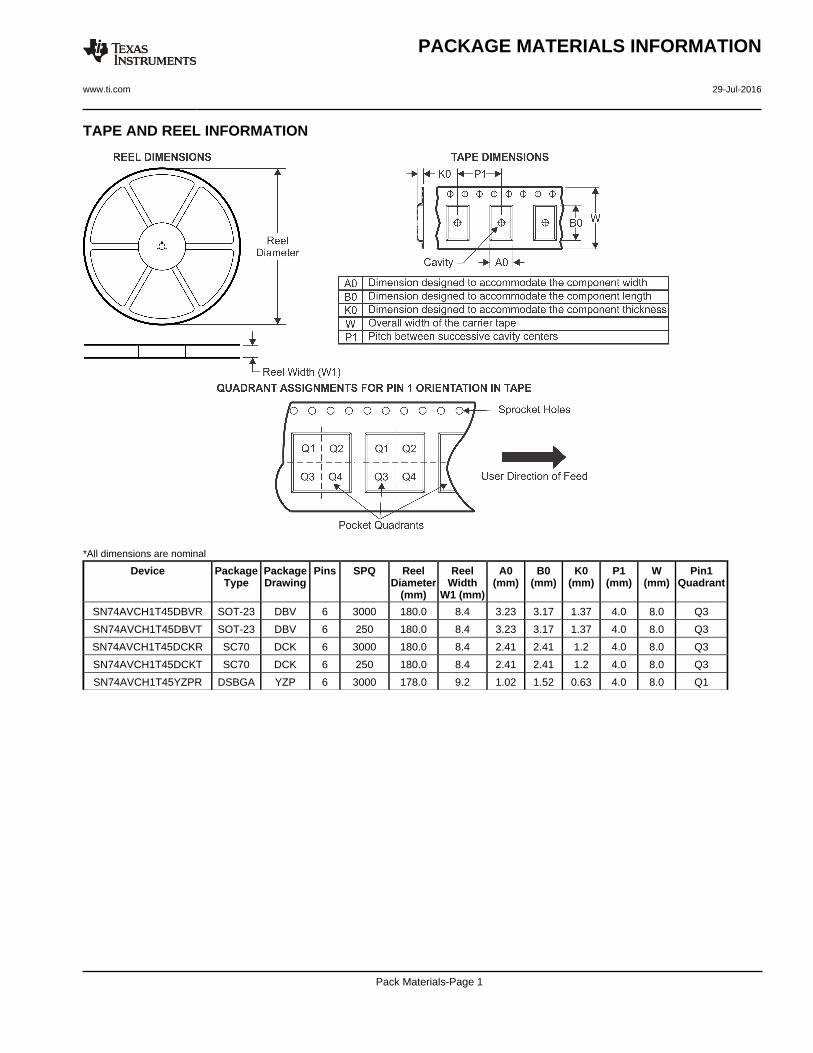
TAPE AND REEL INFORMATION
*All dimensions are nominal
Device PackageType
PackageDrawing
Pins SPQ ReelDiameter
(mm)
ReelWidth
W1 (mm)
A0(mm)
B0(mm)
K0(mm)
P1(mm)
W(mm)
Pin1Quadrant
SN74AVCH1T45DBVR SOT-23 DBV 6 3000 180.0 8.4 3.23 3.17 1.37 4.0 8.0 Q3
SN74AVCH1T45DBVT SOT-23 DBV 6 250 180.0 8.4 3.23 3.17 1.37 4.0 8.0 Q3
SN74AVCH1T45DCKR SC70 DCK 6 3000 180.0 8.4 2.41 2.41 1.2 4.0 8.0 Q3
SN74AVCH1T45DCKT SC70 DCK 6 250 180.0 8.4 2.41 2.41 1.2 4.0 8.0 Q3
SN74AVCH1T45YZPR DSBGA YZP 6 3000 178.0 9.2 1.02 1.52 0.63 4.0 8.0 Q1
PACKAGE MATERIALS INFORMATION
www.ti.com 29-Jul-2016
Pack Materials-Page 1
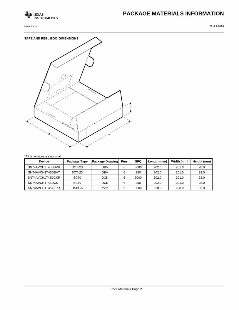
*All dimensions are nominal
Device Package Type Package Drawing Pins SPQ Length (mm) Width (mm) Height (mm)
SN74AVCH1T45DBVR SOT-23 DBV 6 3000 202.0 201.0 28.0
SN74AVCH1T45DBVT SOT-23 DBV 6 250 202.0 201.0 28.0
SN74AVCH1T45DCKR SC70 DCK 6 3000 202.0 201.0 28.0
SN74AVCH1T45DCKT SC70 DCK 6 250 202.0 201.0 28.0
SN74AVCH1T45YZPR DSBGA YZP 6 3000 220.0 220.0 35.0
PACKAGE MATERIALS INFORMATION
www.ti.com 29-Jul-2016
Pack Materials-Page 2


www.ti.com
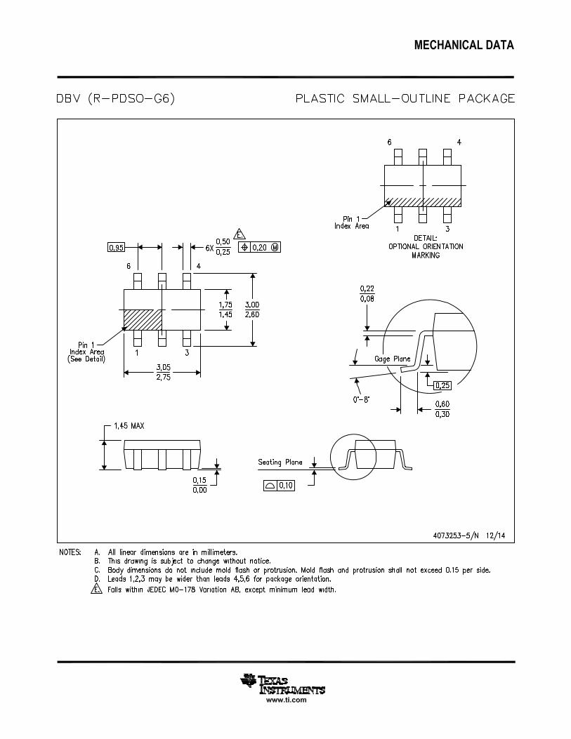
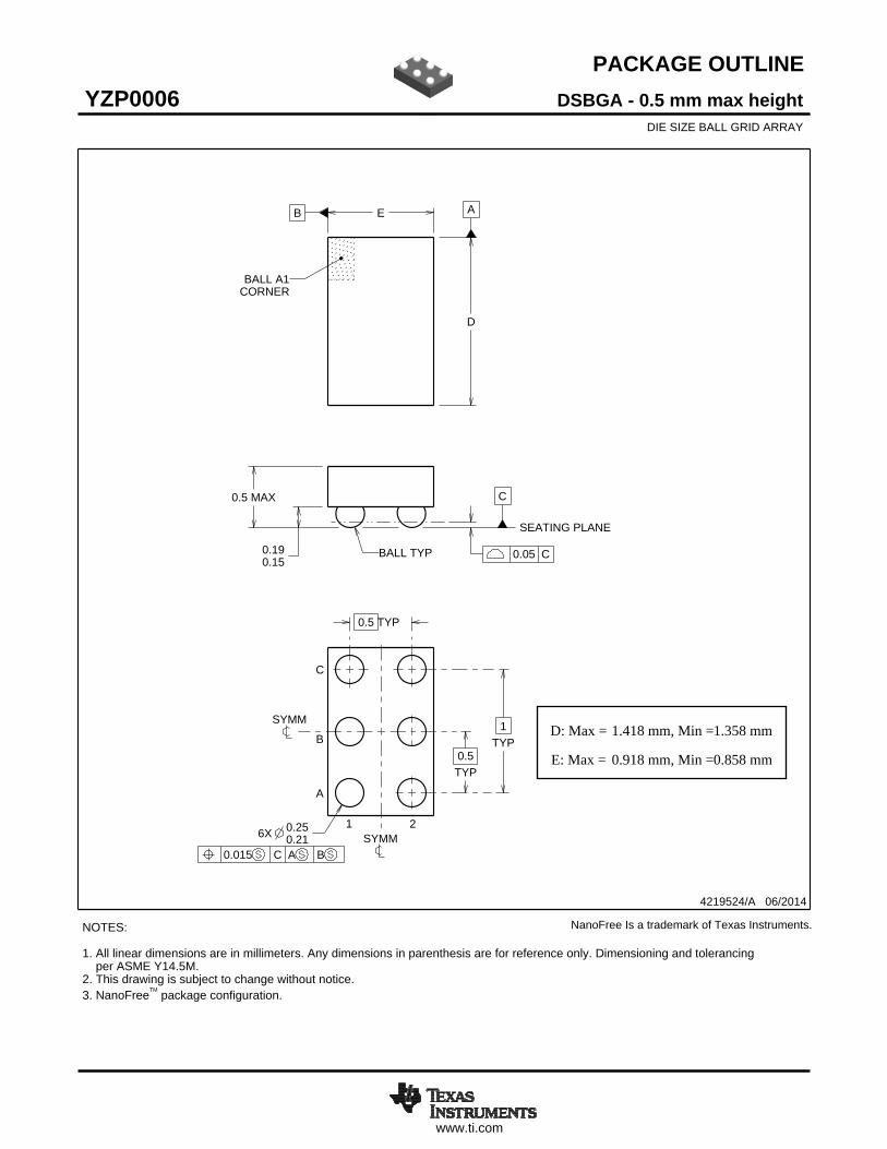
PACKAGE OUTLINE
C0.5 MAX
0.190.15
1TYP
0.5 TYP
6X 0.250.21
0.5TYP
B E A
D
4219524/A 06/2014
DSBGA - 0.5 mm max heightYZP0006DIE SIZE BALL GRID ARRAY
NOTES: 1. All linear dimensions are in millimeters. Any dimensions in parenthesis are for reference only. Dimensioning and tolerancing per ASME Y14.5M.2. This drawing is subject to change without notice.3. NanoFreeTM package configuration.
NanoFree Is a trademark of Texas Instruments.
BALL A1CORNER
SEATING PLANE
BALL TYP 0.05 C
B
A
1 2
0.015 C A B
SYMM
SYMM
C
SCALE 9.000
D: Max =
E: Max =
1.418 mm, Min =
0.918 mm, Min =
1.358 mm
0.858 mm
www.ti.com
EXAMPLE BOARD LAYOUT
6X ( )0.225(0.5) TYP
(0.5) TYP
( )METAL0.225 0.05 MAX
SOLDER MASKOPENING
METALUNDERMASK
( )SOLDER MASKOPENING
0.225
0.05 MIN
4219524/A 06/2014
DSBGA - 0.5 mm max heightYZP0006DIE SIZE BALL GRID ARRAY
NOTES: (continued) 4. Final dimensions may vary due to manufacturing tolerance considerations and also routing constraints. For more information, see Texas Instruments literature number SBVA017 (www.ti.com/lit/sbva017).
SYMM
SYMM
LAND PATTERN EXAMPLESCALE:40X
1 2
A
B
C
NON-SOLDER MASKDEFINED
(PREFERRED)
SOLDER MASK DETAILSNOT TO SCALE
SOLDER MASKDEFINED
www.ti.com
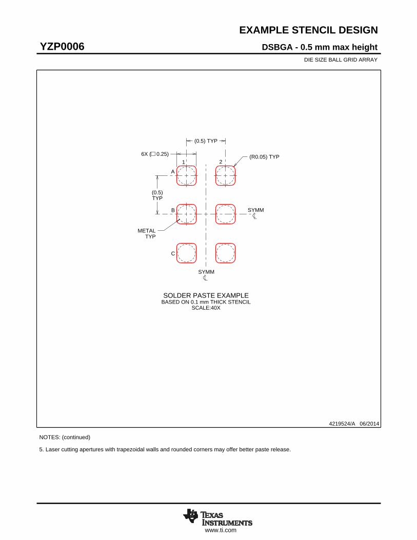
EXAMPLE STENCIL DESIGN
(0.5)TYP
(0.5) TYP
6X ( 0.25) (R ) TYP0.05
METALTYP
4219524/A 06/2014
DSBGA - 0.5 mm max heightYZP0006DIE SIZE BALL GRID ARRAY
NOTES: (continued) 5. Laser cutting apertures with trapezoidal walls and rounded corners may offer better paste release.
SYMM
SYMM
SOLDER PASTE EXAMPLEBASED ON 0.1 mm THICK STENCIL
SCALE:40X
1 2
A
B
C

IMPORTANT NOTICE FOR TI DESIGN INFORMATION AND RESOURCES
Texas Instruments Incorporated (‘TI”) technical, application or other design advice, services or information, including, but not limited to,reference designs and materials relating to evaluation modules, (collectively, “TI Resources”) are intended to assist designers who aredeveloping applications that incorporate TI products; by downloading, accessing or using any particular TI Resource in any way, you(individually or, if you are acting on behalf of a company, your company) agree to use it solely for this purpose and subject to the terms ofthis Notice.TI’s provision of TI Resources does not expand or otherwise alter TI’s applicable published warranties or warranty disclaimers for TIproducts, and no additional obligations or liabilities arise from TI providing such TI Resources. TI reserves the right to make corrections,enhancements, improvements and other changes to its TI Resources.You understand and agree that you remain responsible for using your independent analysis, evaluation and judgment in designing yourapplications and that you have full and exclusive responsibility to assure the safety of your applications and compliance of your applications(and of all TI products used in or for your applications) with all applicable regulations, laws and other applicable requirements. Yourepresent that, with respect to your applications, you have all the necessary expertise to create and implement safeguards that (1)anticipate dangerous consequences of failures, (2) monitor failures and their consequences, and (3) lessen the likelihood of failures thatmight cause harm and take appropriate actions. You agree that prior to using or distributing any applications that include TI products, youwill thoroughly test such applications and the functionality of such TI products as used in such applications. TI has not conducted anytesting other than that specifically described in the published documentation for a particular TI Resource.You are authorized to use, copy and modify any individual TI Resource only in connection with the development of applications that includethe TI product(s) identified in such TI Resource. NO OTHER LICENSE, EXPRESS OR IMPLIED, BY ESTOPPEL OR OTHERWISE TOANY OTHER TI INTELLECTUAL PROPERTY RIGHT, AND NO LICENSE TO ANY TECHNOLOGY OR INTELLECTUAL PROPERTYRIGHT OF TI OR ANY THIRD PARTY IS GRANTED HEREIN, including but not limited to any patent right, copyright, mask work right, orother intellectual property right relating to any combination, machine, or process in which TI products or services are used. Informationregarding or referencing third-party products or services does not constitute a license to use such products or services, or a warranty orendorsement thereof. Use of TI Resources may require a license from a third party under the patents or other intellectual property of thethird party, or a license from TI under the patents or other intellectual property of TI.TI RESOURCES ARE PROVIDED “AS IS” AND WITH ALL FAULTS. TI DISCLAIMS ALL OTHER WARRANTIES ORREPRESENTATIONS, EXPRESS OR IMPLIED, REGARDING TI RESOURCES OR USE THEREOF, INCLUDING BUT NOT LIMITED TOACCURACY OR COMPLETENESS, TITLE, ANY EPIDEMIC FAILURE WARRANTY AND ANY IMPLIED WARRANTIES OFMERCHANTABILITY, FITNESS FOR A PARTICULAR PURPOSE, AND NON-INFRINGEMENT OF ANY THIRD PARTY INTELLECTUALPROPERTY RIGHTS.TI SHALL NOT BE LIABLE FOR AND SHALL NOT DEFEND OR INDEMNIFY YOU AGAINST ANY CLAIM, INCLUDING BUT NOTLIMITED TO ANY INFRINGEMENT CLAIM THAT RELATES TO OR IS BASED ON ANY COMBINATION OF PRODUCTS EVEN IFDESCRIBED IN TI RESOURCES OR OTHERWISE. IN NO EVENT SHALL TI BE LIABLE FOR ANY ACTUAL, DIRECT, SPECIAL,COLLATERAL, INDIRECT, PUNITIVE, INCIDENTAL, CONSEQUENTIAL OR EXEMPLARY DAMAGES IN CONNECTION WITH ORARISING OUT OF TI RESOURCES OR USE THEREOF, AND REGARDLESS OF WHETHER TI HAS BEEN ADVISED OF THEPOSSIBILITY OF SUCH DAMAGES.You agree to fully indemnify TI and its representatives against any damages, costs, losses, and/or liabilities arising out of your non-compliance with the terms and provisions of this Notice.This Notice applies to TI Resources. Additional terms apply to the use and purchase of certain types of materials, TI products and services.These include; without limitation, TI’s standard terms for semiconductor products http://www.ti.com/sc/docs/stdterms.htm), evaluationmodules, and samples (http://www.ti.com/sc/docs/sampterms.htm).
Mailing Address: Texas Instruments, Post Office Box 655303, Dallas, Texas 75265Copyright © 2017, Texas Instruments Incorporated