scattering parameters - rfic - university of california, berkeley
TRANSCRIPT

EECS 242
Scattering Parameters
Prof. Niknejad
University of California, Berkeley
University of California, Berkeley EECS 242 – p. 1/43
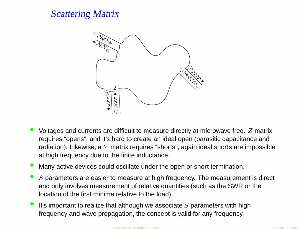
Scattering Matrix
1
2
3
V+1
V−
1
V+2
V−
2
V+3
V−
3
• Voltages and currents are difficult to measure directly at microwave freq. Z matrixrequires “opens”, and it’s hard to create an ideal open (parasitic capacitance andradiation). Likewise, a Y matrix requires “shorts”, again ideal shorts are impossibleat high frequency due to the finite inductance.
• Many active devices could oscillate under the open or short termination.
• S parameters are easier to measure at high frequency. The measurement is directand only involves measurement of relative quantities (such as the SWR or thelocation of the first minima relative to the load).
• It’s important to realize that although we associate S parameters with highfrequency and wave propagation, the concept is valid for any frequency.
University of California, Berkeley EECS 242 – p. 2/43
Power Flow in an One-Port
•• The concept of scattering parameters is very closely related to the concept ofpower flow. For this reason, we begin with the simple observation that the powerflow into a one-port circuit can be written in the following form
Pin = Pavs − Pr
• where Pavs is the available power from the source. Unless otherwise stated, let usassume sinusoidal steady-state. If the source has a real resistance of Z0, this issimply given by
Pavs =V 2
s
8Z0
• Of course if the one-port is conjugately matched to the source, then it will draw themaximal available power from the source. Otherwise, the power Pin is always lessthan Pavs, which is reflected in our equation. In general, Pr represents the wastedor untapped power that one-port circuit is “reflecting” back to the source due to amismatch. For passive circuits it’s clear that each term in the equation is positiveand Pin ≥ 0.
University of California, Berkeley EECS 242 – p. 3/43

Power Absorbed by One-Port
• The complex power absorbed by the one-port is given by
Pin =1
2(V1 · I∗1 + V ∗
1 · I1)
• which allows us to write
Pr = Pavs − Pin =V 2
s
4Z0− 1
2(V1I∗1 + V ∗
1 I1)
• the factor of 4 instead of 8 is used since we are now dealing with complex power.The average power can be obtained by taking one half of the real component ofthe complex power. If the one-port has an input impedance of Zin, then the powerPin is expanded to
Pin =1
2
„
Zin
Zin + Z0Vs · V ∗
s
(Zin + Z0)∗+
Z∗in
(Zin + Z0)∗V ∗
s · Vs
(Zin + Z0)
«
• which is easily simplified to (where we have assumed Z0 is real)
Pin =|Vs|22Z0
„
Z0Zin + Z∗inZ0
|Zin + Z0|2«
University of California, Berkeley EECS 242 – p. 4/43
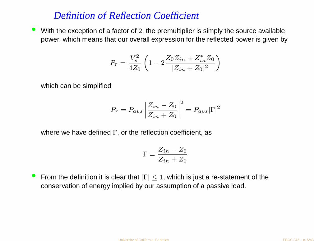
Definition of Reflection Coefficient• With the exception of a factor of 2, the premultiplier is simply the source available
power, which means that our overall expression for the reflected power is given by
Pr =V 2
s
4Z0
„
1 − 2Z0Zin + Z∗
inZ0
|Zin + Z0|2«
which can be simplified
Pr = Pavs
˛
˛
˛
˛
Zin − Z0
Zin + Z0
˛
˛
˛
˛
2
= Pavs|Γ|2
where we have defined Γ, or the reflection coefficient, as
Γ =Zin − Z0
Zin + Z0
• From the definition it is clear that |Γ| ≤ 1, which is just a re-statement of theconservation of energy implied by our assumption of a passive load.
University of California, Berkeley EECS 242 – p. 5/43

Scattering Parameter• This constant Γ, also called the scattering parameter of a one-port, plays a very
important role. On one hand we see that it is has a one-to-one relationship withZin. Given Γ we can solve for Zin by inverting the above equation
Zin = Z01 + Γ
1 − Γ
which means that all of the information in Zin is also in Γ. Moreover, since |Γ| < 1,we see that the space of the semi-infinite space of all impedance values with realpositive components (the right-half plane) maps into the unit circle. This is a greatcompression of information which allows us to visualize the entire space ofrealizable impedance values by simply observing the unit circle. We shall find wideapplication for this concept when finding the appropriate load/source impedancefor an amplifier to meet a given noise or gain specification.
• More importantly, Γ expresses very direct and obviously the power flow in thecircuit. If Γ = 0, then the one-port is absorbing all the possible power availablefrom the source. If |Γ| = 1 then the one-port is not absorbing any power, but rather“reflecting” the power back to the source. Clearly an open circuit, short circuit, or areactive load cannot absorb net power. For an open and short load, this is obviousfrom the definition of Γ. For a reactive load, this is pretty clear if we substituteZin = jX
|ΓX | =
˛
˛
˛
˛
jX − Z0
jX + Z0
˛
˛
˛
˛
=
˛
˛
˛
˛
˛
˛
˛
q
X2 + Z20
q
X2 + Z20
˛
˛
˛
˛
˛
˛
˛
= 1
University of California, Berkeley EECS 242 – p. 6/43

Relation between Z andΓ
• The transformation between impedance and Γ is a well known mathematicaltransform (see Bilinear Transform). It is a conformal mapping (meaning that itpreserves angles) which maps vertical and horizontal lines in the impedance planeinto circles. We have already seen that the jX axis is mapped onto the unit circle.Since |Γ|2 represents power flow, we may imagine that Γ should represent the flowof voltage, current, or some linear combination thereof. Consider taking the squareroot of the basic equation we have derived
p
Pr = Γp
Pavs
where we have retained the positive root. We may write the above equation as
b1 = Γa1
where a and b have the units of square root of power and represent signal flow inthe network. How are a and b related to currents and voltage?
University of California, Berkeley EECS 242 – p. 7/43
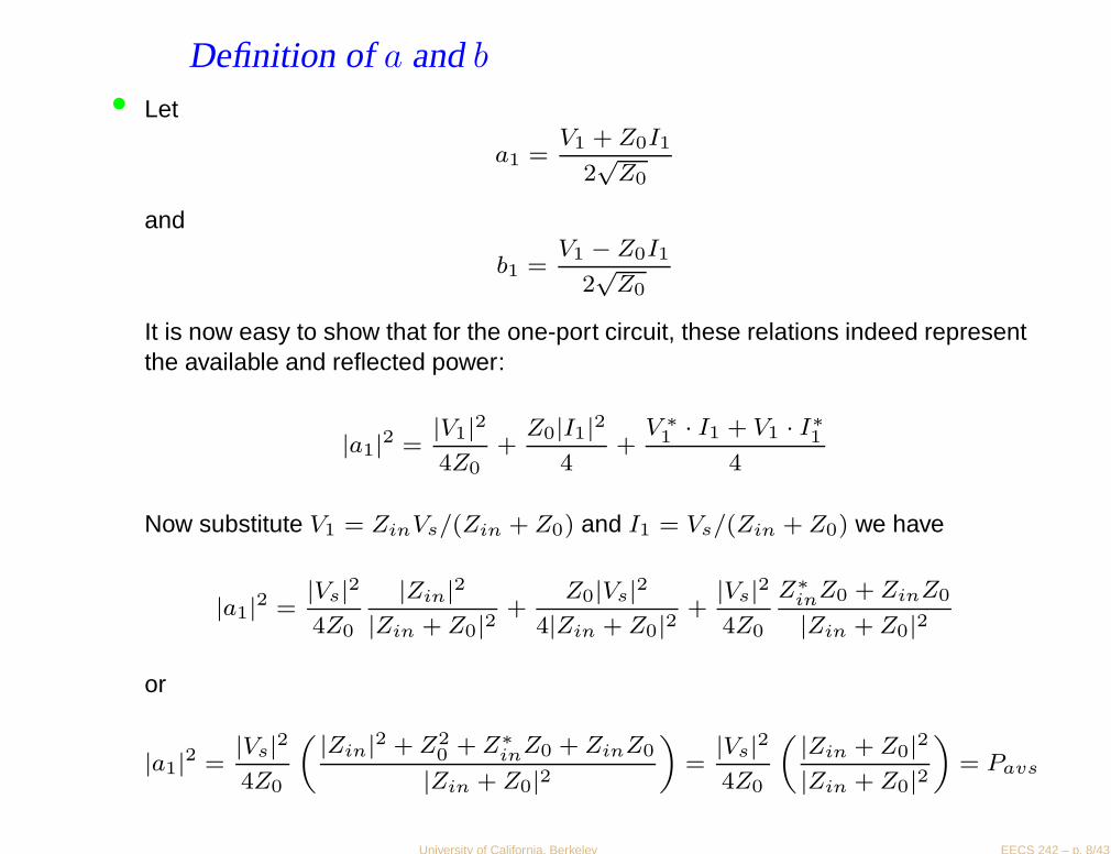
Definition ofa andb
• Let
a1 =V1 + Z0I1
2√
Z0
and
b1 =V1 − Z0I1
2√
Z0
It is now easy to show that for the one-port circuit, these relations indeed representthe available and reflected power:
|a1|2 =|V1|24Z0
+Z0|I1|2
4+
V ∗1 · I1 + V1 · I∗1
4
Now substitute V1 = ZinVs/(Zin + Z0) and I1 = Vs/(Zin + Z0) we have
|a1|2 =|Vs|24Z0
|Zin|2|Zin + Z0|2
+Z0|Vs|2
4|Zin + Z0|2+
|Vs|24Z0
Z∗inZ0 + ZinZ0
|Zin + Z0|2
or
|a1|2 =|Vs|24Z0
„ |Zin|2 + Z20 + Z∗
inZ0 + ZinZ0
|Zin + Z0|2«
=|Vs|24Z0
„ |Zin + Z0|2|Zin + Z0|2
«
= Pavs
University of California, Berkeley EECS 242 – p. 8/43

Relationship betwena/b and Power Flow• In a like manner, the square of b is given by many similar terms
|b1|2 =|Vs|24Z0
„ |Zin|2 + Z20 − Z∗
inZ0 − ZinZ0
|Zin + Z0|2«
= Pavs
˛
˛
˛
˛
|Zin − Z0
Zin + Z0
˛
˛
˛
˛
2
= Pavs|Γ|2
= |a1|2|Γ|2
as expected. We can now see that the expression b = Γ · a is analogous to theexpression V = Z · I or I = Y ·V and so it can be generalized to an N -port circuit.In fact, since a and b are linear combinations of v and i, there is a one-to-onerelationship between the two. Taking the sum and difference of a and b we arrive at
a1 + b1 =2V1
2√
Z0=
V1√Z0
which is related to the port voltage and
a1 − b1 =2Z0I1
2√
Z0=p
Z0I1
which is related to the port current.
University of California, Berkeley EECS 242 – p. 9/43

Incident and Scattering Waves
• Let’s define the vector v+ as the incident “forward” waves on each transmissionline connected to the N port. Define the reference plane as the point where thetransmission line terminates onto the N port.
• The vector v− is then the reflected or “scattered” waveform at the location of theport.
v+ =
0
B
B
B
B
@
V +1
V +2
V +3
...
1
C
C
C
C
A
v− =
0
B
B
B
B
@
V −1
V −2
V −3
...
1
C
C
C
C
A
• Because the N port is linear, we expect that scattered field to be a linear functionof the incident field
v− = Sv+
• S is the scattering matrix
S =
0
B
B
B
@
S11 S12 · · ·
S21
. . ....
1
C
C
C
A
University of California, Berkeley EECS 242 – p. 10/43

Relation to Voltages
• The fact that the S matrix exists can be easily proved if we recall that the voltageand current on each transmission line termination can be written as
Vi = V +i + V −
i Ii = Y0(I+i − I−i )
• Inverting these equations
Vi + Z0Ii = V +i + V −
i + V +i − V −
i = 2V +i
Vi − Z0Ii = V +i + V −
i − V +i + V −
i = 2V −i
• Thus v+,v− are simply linear combinations of the port voltages and currents. Bythe uniqueness theorem, then, v− = Sv+.
University of California, Berkeley EECS 242 – p. 11/43

MeasureSij
1
2
3
V+1
V−
1
V−
2
V−
3
4
5
6
Z0
Z0
Z0
Z0
Z0
• The term Sij can be computed directly by the following formula
Sij =V −
i
V +j
˛
˛
˛
˛
˛
V+
k=0 ∀ k 6=j
• In other words, to measure Sij , drive port j with a wave amplitude of V +j and
terminate all other ports with the characteristic impedance of the lines (so thatV +
k= 0 for k 6= j). Then observe the wave amplitude coming out of the port i
University of California, Berkeley EECS 242 – p. 12/43
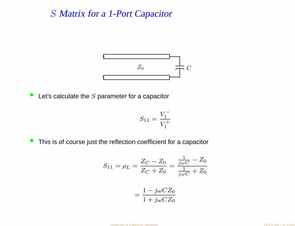
S Matrix for a 1-Port Capacitor
Z0 C
• Let’s calculate the S parameter for a capacitor
S11 =V −1
V +1
• This is of course just the reflection coefficient for a capacitor
S11 = ρL =ZC − Z0
ZC + Z0=
1jωC
− Z0
1jωC
+ Z0
=1 − jωCZ0
1 + jωCZ0
University of California, Berkeley EECS 242 – p. 13/43
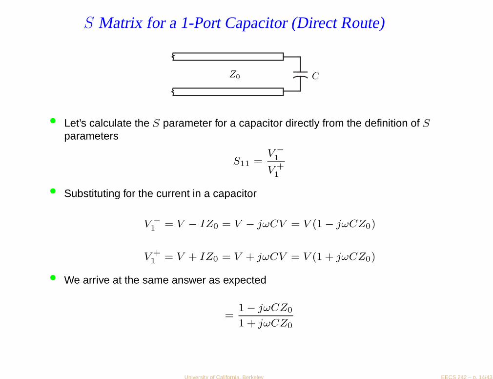
S Matrix for a 1-Port Capacitor (Direct Route)
Z0 C
• Let’s calculate the S parameter for a capacitor directly from the definition of Sparameters
S11 =V −1
V +1
• Substituting for the current in a capacitor
V −1 = V − IZ0 = V − jωCV = V (1 − jωCZ0)
V +1 = V + IZ0 = V + jωCV = V (1 + jωCZ0)
• We arrive at the same answer as expected
=1 − jωCZ0
1 + jωCZ0
University of California, Berkeley EECS 242 – p. 14/43
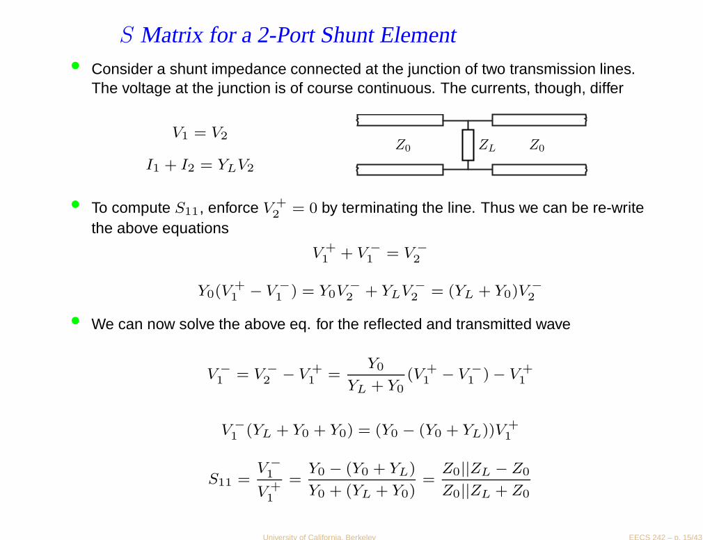
S Matrix for a 2-Port Shunt Element• Consider a shunt impedance connected at the junction of two transmission lines.
The voltage at the junction is of course continuous. The currents, though, differ
V1 = V2
I1 + I2 = YLV2
Z0 Z0ZL
• To compute S11, enforce V +2 = 0 by terminating the line. Thus we can be re-write
the above equations
V +1 + V −
1 = V −2
Y0(V+1 − V −
1 ) = Y0V −2 + YLV −
2 = (YL + Y0)V −2
• We can now solve the above eq. for the reflected and transmitted wave
V −1 = V −
2 − V +1 =
Y0
YL + Y0(V +
1 − V −1 ) − V +
1
V −1 (YL + Y0 + Y0) = (Y0 − (Y0 + YL))V +
1
S11 =V −1
V +1
=Y0 − (Y0 + YL)
Y0 + (YL + Y0)=
Z0||ZL − Z0
Z0||ZL + Z0
University of California, Berkeley EECS 242 – p. 15/43
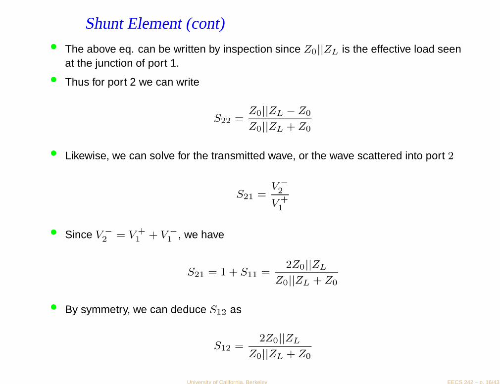
Shunt Element (cont)• The above eq. can be written by inspection since Z0||ZL is the effective load seen
at the junction of port 1.
• Thus for port 2 we can write
S22 =Z0||ZL − Z0
Z0||ZL + Z0
• Likewise, we can solve for the transmitted wave, or the wave scattered into port 2
S21 =V −2
V +1
• Since V −2 = V +
1 + V −1 , we have
S21 = 1 + S11 =2Z0||ZL
Z0||ZL + Z0
• By symmetry, we can deduce S12 as
S12 =2Z0||ZL
Z0||ZL + Z0
University of California, Berkeley EECS 242 – p. 16/43

Conversion Formula• Since V + and V − are related to V and I, it’s easy to find a formula to convert for
Z or Y to S
Vi = V +i + V −
i → v = v+ + v−
Zi0Ii = V +i − V −
i → Z0i = v+ − v−
• Now starting with v = Zi, we have
v+ + v− = ZZ−10 (v+ − v−)
• Note that Z0 is the scalar port impedance
v−(I + ZZ−10 ) = (ZZ−1
0 − I)v+
v− = (I + ZZ−10 )−1(ZZ−1
0 − I)v+ = Sv+
• We now have a formula relating the Z matrix to the S matrix
S = (ZZ−10 + I)−1(ZZ−1
0 − I) = (Z + Z0I)−1(Z − Z0I)
University of California, Berkeley EECS 242 – p. 17/43

Conversion (cont)
• Recall that the reflection coefficient for a load is given by the same equation!
ρ =Z/Z0 − 1
Z/Z0 + 1
• To solve for Z in terms of S, simply invert the relation
Z−10 ZS + IS = Z−1
0 Z − I
Z−10 Z(I − S) = S + I
Z = Z0(I + S)(I − S)−1
• As expected, these equations degenerate into the correct form for a 1 × 1 system
Z11 = Z01 + S11
1 − S11
University of California, Berkeley EECS 242 – p. 18/43

Reciprocal Networks• We have found that the Z and Y matrix are symmetric. Now let’s see what we can
infer about the S matrix.
v+ =1
2(v + Z0i)
v− =1
2(v − Z0i)
• Substitute v = Zi in the above equations
v+ =1
2(Zi + Z0i) =
1
2(Z + Z0)i
v− =1
2(Zi − Z0i) =
1
2(Z − Z0)i
• Since i = i, the above eq. must result in consistent values of i. Or
2(Z + Z0)−1v+ = 2(Z − Z0)−1v−
ThusS = (Z − Z0)(Z + Z0)−1
University of California, Berkeley EECS 242 – p. 19/43

Reciprocal Networks (cont)
• Consider the transpose of the S matrix
St =`
(Z + Z0)−1´t
(Z − Z0)t
• Recall that Z0 is a diagonal matrix
St = (Zt + Z0)−1(Zt − Z0)
• If Zt = Z (reciprocal network), then we have
St = (Z + Z0)−1(Z − Z0)
• Previously we found that
S = (Z + Z0)−1(Z − Z0)
• So that we see that the S matrix is also symmetric (under reciprocity)
St = S
University of California, Berkeley EECS 242 – p. 20/43

Another Proof
• Note that in effect we have shown that
(Z + I)−1(Z − I) = (Z − I)(Z + I)−1
• This is easy to demonstrate if we note that
Z2 − I = Z2 − I2 = (Z + I)(Z − I) = (Z − I)(Z + I)
• In general matrix multiplication does not commute, but here it does
(Z − I) = (Z + I)(Z − I)(Z + I)−1
(Z + I)−1(Z − I) = (Z − I)(Z + I)−1
• Thus we see that St = S.
University of California, Berkeley EECS 242 – p. 21/43
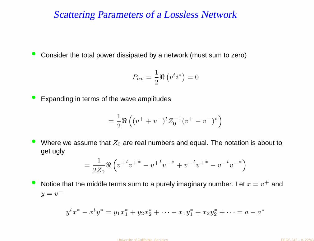
Scattering Parameters of a Lossless Network
• Consider the total power dissipated by a network (must sum to zero)
Pav =1
2ℜ`
vti∗´
= 0
• Expanding in terms of the wave amplitudes
=1
2ℜ“
(v+ + v−)tZ−10 (v+ − v−)∗
”
• Where we assume that Z0 are real numbers and equal. The notation is about toget ugly
=1
2Z0ℜ“
v+tv+∗ − v+t
v−∗
+ v−tv+∗ − v−
tv−
∗”
• Notice that the middle terms sum to a purely imaginary number. Let x = v+ andy = v−
ytx∗ − xty∗ = y1x∗1 + y2x∗
2 + · · · − x1y∗1 + x2y∗
2 + · · · = a − a∗
University of California, Berkeley EECS 242 – p. 22/43
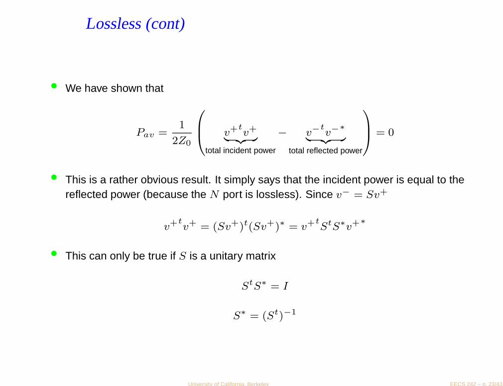
Lossless (cont)
• We have shown that
Pav =1
2Z0
0
B
@v+t
v+| {z }
total incident power
− v−tv−
∗
| {z }
total reflected power
1
C
A= 0
• This is a rather obvious result. It simply says that the incident power is equal to thereflected power (because the N port is lossless). Since v− = Sv+
v+tv+ = (Sv+)t(Sv+)∗ = v+t
StS∗v+∗
• This can only be true if S is a unitary matrix
StS∗ = I
S∗ = (St)−1
University of California, Berkeley EECS 242 – p. 23/43

Orthogonal Properties ofS
• Expanding out the matrix product
δij =X
k
(ST )ikS∗kj =
X
k
SkiS∗kj
• For i = j we haveX
k
SkiS∗ki = 1
• For i 6= j we haveX
k
SkiS∗kj = 0
• The dot product of any column of S with the conjugate of that column is unity whilethe dot product of any column with the conjugate of a different column is zero. Ifthe network is reciprocal, then St = S and the same applies to the rows of S.
• Note also that |Sij | ≤ 1.
University of California, Berkeley EECS 242 – p. 24/43

Shift in Reference Planes
• Note that if we move the reference planes, we can easily recalculate the Sparameters.
• We’ll derive a new matrix S′ related to S. Let’s call the waves at the new referenceν
v− = Sv+
ν− = S′ν+
• Since the waves on the lossless transmission lines only experience a phase shift,we have a phase shift of θi = βiℓi
ν−i = v−e−jθi
ν+i = v+ejθi
University of California, Berkeley EECS 242 – p. 25/43

Reference Plane (cont)
• Or we have
2
6
6
6
6
4
ejθ1 0 · · ·0 ejθ2 · · ·0 0 ejθ3 · · ·...
3
7
7
7
7
5
ν− = S
2
6
6
6
6
4
e−jθ1 0 · · ·0 e−jθ2 · · ·0 0 e−jθ3 · · ·...
3
7
7
7
7
5
ν+
• So we see that the new S matrix is simply
S′ =
2
6
6
6
6
4
e−jθ1 0 · · ·0 e−jθ2 · · ·0 0 e−jθ3 · · ·...
3
7
7
7
7
5
S
2
6
6
6
6
4
e−jθ1 0 · · ·0 e−jθ2 · · ·0 0 e−jθ3 · · ·...
3
7
7
7
7
5
University of California, Berkeley EECS 242 – p. 26/43
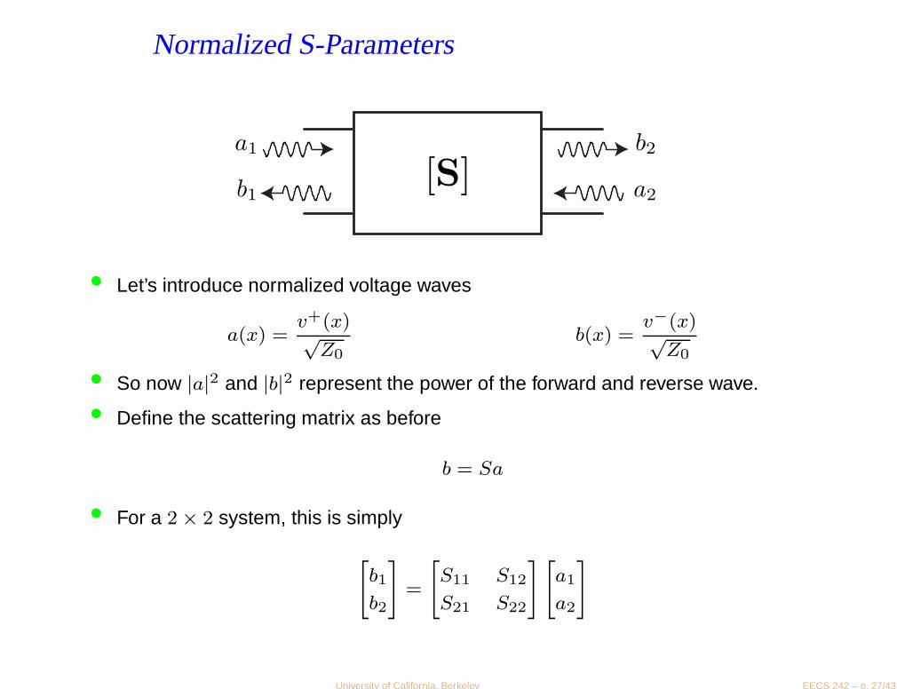
Normalized S-Parameters
a1
a2b1
b2
[S]
• Let’s introduce normalized voltage waves
a(x) =v+(x)√
Z0b(x) =
v−(x)√Z0
• So now |a|2 and |b|2 represent the power of the forward and reverse wave.
• Define the scattering matrix as before
b = Sa
• For a 2 × 2 system, this is simply
"
b1
b2
#
=
"
S11 S12
S21 S22
#"
a1
a2
#
University of California, Berkeley EECS 242 – p. 27/43

Generalized Scattering Parameters• We can use different impedances Z0,n at each port and so we have the
generalized incident and reflected waves
an =v+
np
Z0,n
bn =v−n
p
Z0,n
• The scattering parameters are now given by
Sij =bi
aj
˛
˛
˛
˛
ak 6=j=0
Sij =V −
i
V +j
p
Z0,jp
Z0,i
˛
˛
˛
˛
˛
V+
k 6=j=0
• Consider the current and voltage in terms of a and b
Vn = v+n + v−n =
p
Z0,n(an + bn) In =1
Z0,n
`
v−n − v−n´
=1
p
Z0,n
(an−bn)
• The power flowing into this port is given by
Pn =1
2ℜ (VnI∗n) =
1
2ℜ`
|an|2 − |bn|2 + (bna∗n − b∗nan)
´
• Observe that the last term is purely imaginary so we have
Pn =1
2
`
|an|2 − |bn|2´
University of California, Berkeley EECS 242 – p. 28/43

Scattering Transfer Parameters
a1
a2
b1
b2
[T]
a3
b3
a4
b4
[T]
• Up to now we found it convenient to represent the scattered waves in terms of theincident waves. But what if we wish to cascade two ports as shown?
• Since b2 flows into a′1, and likewise b′1 flows into a2, would it not be convenient if
we defined the a relationship between a1,b1 and b2,a2?
• In other words we have
"
a1
b1
#
=
"
T11 T12
T21 T22
#"
b2
a2
#
• Notice carefully the order of waves (a,b) in reference to the figure above. Thisallows us to cascade matrices
"
a1
b1
#
= T1
"
b2
a2
#
= T1
"
a3
b3
#
= T1T2
"
b4
a4
#
University of California, Berkeley EECS 242 – p. 29/43

Representation of Source
VS
+
Vi
−
ZS IS
Vi = Vs − IsZs
• The voltage source can be represented directly for s-parameter analysis asfollows. First note that
V +i + V −
i = Vs +
V +i
Z0− V −
i
Z0
!
Zs
• Solve these equations for V −i , the power flowing away from the source
V −i = V +
i
Zs − Z0
Zs + Z0+
Z0
Z0 + Zs
Vs
• Dividing each term by√
Z0, we have
V −i√Z0
=V +
i√Z0
Γs +
√Z0
Z0 + Zs
Vsbi = aiΓs + bs
bs = Vs
p
Z0/(Z0 +Zs)
University of California, Berkeley EECS 242 – p. 30/43

Available Power from Source
• A useful quantity is the available power from a source under conjugate matchedconditions. Since
Pavs = |bi|2 − |ai|2
• If we let ΓL = Γ∗S , then using ai = ΓLbi, we have
bi = bs + aiΓS = bs + Γ∗SbiΓS
• Solving for bi we have
bi =bs
1 − |ΓS |2
• So the Pavs is given by
Pavs = |bi|2 − |ai|2 = |bs|2„
1 − |ΓS |2(1 − |ΓS |2)2
«
=|bs|2
1 − |ΓS |2
University of California, Berkeley EECS 242 – p. 31/43
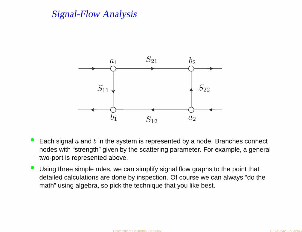
Signal-Flow Analysis
a1
a2b1
b2
S11 S22
S12
S21
• Each signal a and b in the system is represented by a node. Branches connectnodes with “strength” given by the scattering parameter. For example, a generaltwo-port is represented above.
• Using three simple rules, we can simplify signal flow graphs to the point thatdetailed calculations are done by inspection. Of course we can always “do themath” using algebra, so pick the technique that you like best.
University of California, Berkeley EECS 242 – p. 32/43

Series and Parallel Rules
a1 a2
SBSA
a3 a1
SBSA
a3
• Rule 1: (series rule) By inspection, we have the cascade.
a1 a2
SB
SA
a1 a2
SA + SB
• Rule 2: (parallel rule) Clear by inspection.
University of California, Berkeley EECS 242 – p. 33/43

Self-Loop Rule
a1 a2
SCSA
a3
SB
a1 a2
SC
a3
SA
1 − SB
• Rule 3: (self-loop rule) We can remove a “self-loop” by multiplying branchesfeeding the node by 1/(1 − SB) since
a2 = SAa1 + SBa2
a2(1 − SB) = SAa1
a2 =SA
1 − SB
a1
University of California, Berkeley EECS 242 – p. 34/43
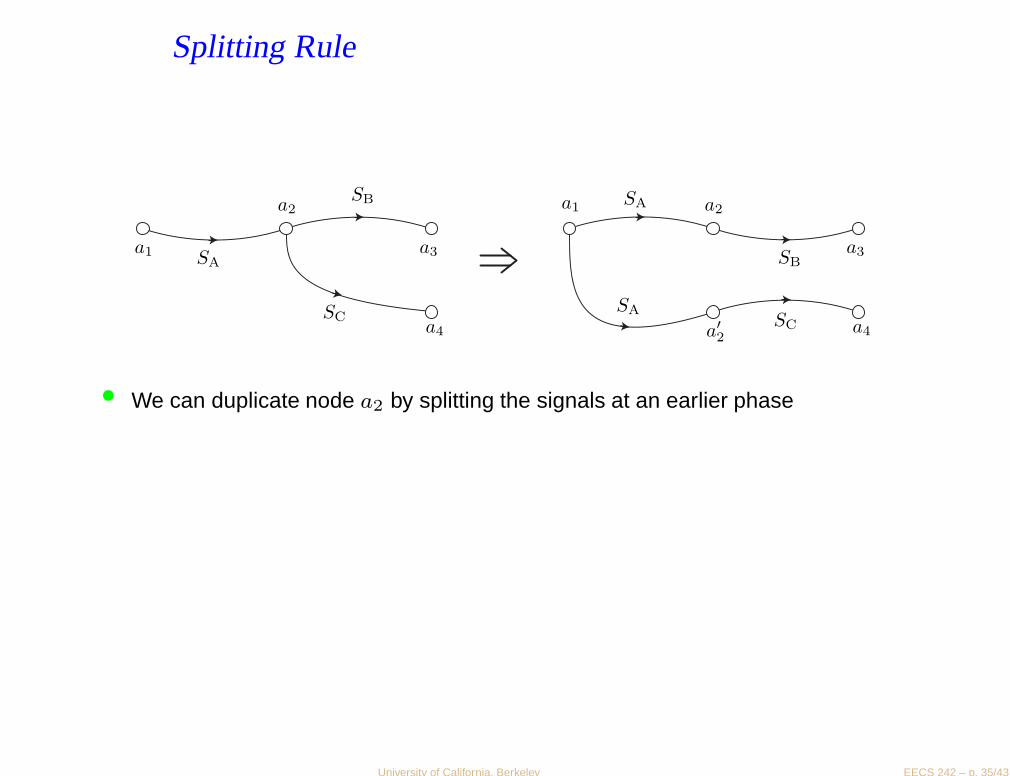
Splitting Rule
a1
a2SB
SAa3
a4
SC
a1 a2
SB
SA
a3
a4SC
SA
a′
2
• We can duplicate node a2 by splitting the signals at an earlier phase
University of California, Berkeley EECS 242 – p. 35/43

Signal Flow Analysis Example
a1
a2b1
b2
S11 S22
S12
S21
ΓL
a1
a2b1
b2
S11
S22
S12
S21
ΓL
ΓL
• Using the above rules, we can calculate the input reflection coefficient of atwo-port terminated by ΓL = b1/a1 using a couple of steps.
• First we notice that there is a self-loop around b2.
a1
a2b1
b2
S11
S12
ΓL
S21
1 − S22ΓL
• Next we remove the self loop and from here it’s clear that the
Γin =b1
a1= S11 +
S21S12ΓL
1 − S22ΓL
University of California, Berkeley EECS 242 – p. 36/43

Mason’s Rule
a1
a2b1
b2
S11S22
S12
S21
ΓLΓS
bS
P1 P2
• Using Mason’s Rule, you can calculate the transfer function for a signal flow graphby “inspection”
T =P1
`
1 −PL(1)(1) +PL(2)(1) − · · ·
´
+ P2
`
1 −PL(1)(2) + · · ·´
+ · · ·1 −PL(1) +
PL(2) −PL(3) + · · ·
• Each Pi defines a path, a directed route from the input to the output not containingeach node more than once. The value of Pi is the product of the branchcoefficients along the path.
• For instance the path from bs to b1 (T = b1/bs) has two paths, P1 = S11 andP2 = S21ΓLS12
University of California, Berkeley EECS 242 – p. 37/43

Loop of Order Summation Notation
a1
a2b1
b2
S11S22
S12
S21
ΓLΓS
bS
a1
b
2
• The notationPL(1) is the sum over all first order loops.
• A “first order loop” is defined as product of the branch values in a loop in the graph.For the given example we have ΓsS11, S22ΓL, and ΓsS21ΓLS12.
• A “second order loop” L(2) is the product of two non-touching first-order loops. Forinstance, since loops S11Γs and S22ΓL do not touch, their product is a secondorder loop.
• A “third order loop” L(3) is likewise the product of three non-touching first orderloops.
• The notationPL(1)(p) is the sum of all first-order loops that do not touch the path
p.
• For path P1, we haveP
L(1)(1) = ΓLS22 but for path P2 we haveP
L(1)(2) = 0.
University of California, Berkeley EECS 242 – p. 38/43
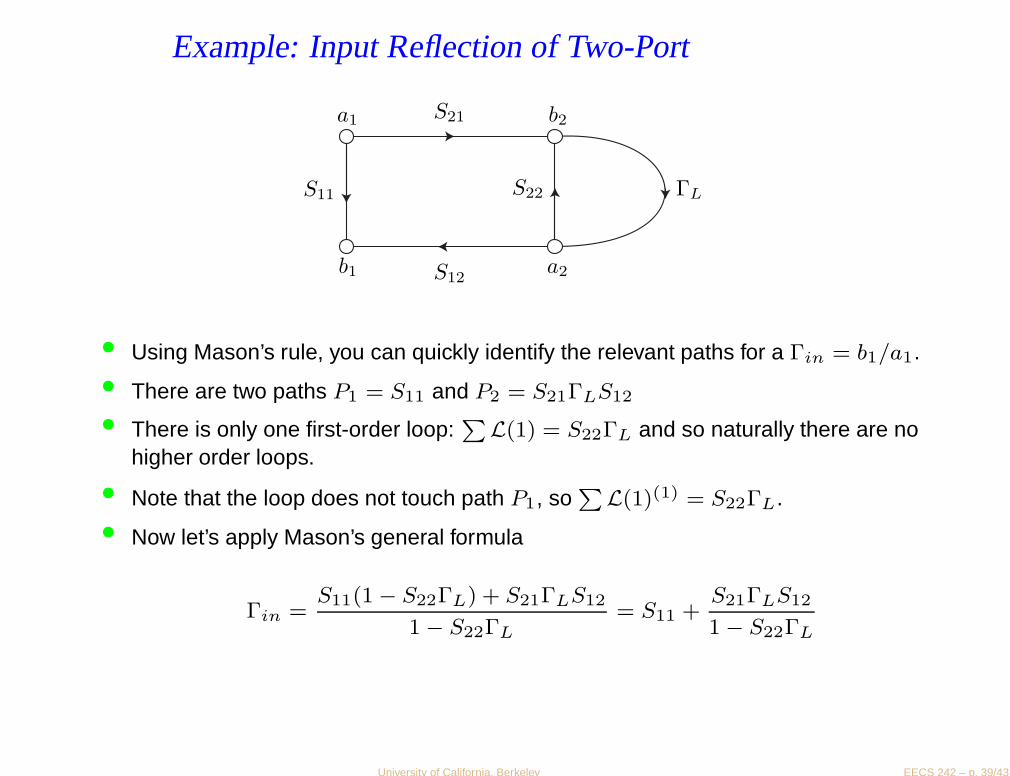
Example: Input Reflection of Two-Port
a1
a2b1
b2
S11 S22
S12
S21
ΓL
• Using Mason’s rule, you can quickly identify the relevant paths for a Γin = b1/a1.
• There are two paths P1 = S11 and P2 = S21ΓLS12
• There is only one first-order loop:PL(1) = S22ΓL and so naturally there are no
higher order loops.
• Note that the loop does not touch path P1, soPL(1)(1) = S22ΓL.
• Now let’s apply Mason’s general formula
Γin =S11(1 − S22ΓL) + S21ΓLS12
1 − S22ΓL
= S11 +S21ΓLS12
1 − S22ΓL
University of California, Berkeley EECS 242 – p. 39/43

Example: Transducer Power Gain
a1
a2b1
b2
S11S22
S12
S21
ΓLΓS
bS
• By definition, the transducer power gain is given by
GT =PL
PAV S
=|b2|2(1 − |ΓL|2)
|bs|2
1−|ΓS |2
=
˛
˛
˛
˛
b2
bS
˛
˛
˛
˛
2
(1 − |ΓL|2)(1 − |ΓS |2)
• By Mason’s Rule, there is only one path P1 = S21 from bS to b2 so we have
X
L(1) = ΓSS11 + S22ΓL + ΓSS21ΓLS12
X
L(2) = ΓSS11ΓLS22
X
L(1)(1) = 0
University of California, Berkeley EECS 242 – p. 40/43

Transducer Gain (cont)• The gain expression is thus given by
b2
bS
=S21(1 − 0)
1 − ΓSS11 − S22ΓL − ΓSS21ΓLS12 + ΓSS11ΓLS22
• The denominator is in the form of 1 − x − y + xy which allows us to write
GT =|S21|2(1 − |ΓS |2)(1 − |ΓL|2)
|(1 − S11ΓS)(1 − S22ΓL) − S21S12ΓLΓS |2
• Recall that Γin = S11 + S21S12ΓL/(1 − S22ΓL). Factoring out 1 − S22ΓL fromthe denominator we have
den =
„
1 − S11ΓS − S21S12ΓL
1 − S22ΓL
ΓS
«
(1 − S22ΓL)
den =
„
1 − ΓS
„
S11 +S21S12ΓL
1 − S22ΓL
««
(1 − S22ΓL)
= (1 − ΓSΓin)(1 − S22ΓL)
University of California, Berkeley EECS 242 – p. 41/43

Transducer Gain Expression
• This simplifications allows us to write the transducer gain in the followingconvenient form
GT =1 − |ΓS |2
|1 − ΓinΓS |2|S21|2
1 − |ΓL|2|1 − S22ΓL|2
• Which can be viewed as a product of the action of the input match “gain", theintrinsic two-port gain |S21|2, and the output match “gain". Since the generaltwo-port is not unilateral, the input match is a function of the load.
• Likewise, by symmetry we can also factor the expression to obtain
GT =1 − |ΓS |2
|1 − S11ΓS |2|S21|2
1 − |ΓL|2|1 − ΓoutΓL|2
University of California, Berkeley EECS 242 – p. 42/43

Refs
• “S Parameter Design,” Hewlett-Packard Application Note 154, April 1972.
• Microwave Transistor Amplifiers, Analysis and Design, Guillermo Gonzalez,Prentice Hall 1984.
• Microwave Engineering, David Pozer, Third Edition, Wiley 2005.
• Microwave Circuit Design Using Linear and Nonlinear Techniques, by GeorgeVendelin, Anthony M. Pavio, & Ulrich L. Rohde, Wiley 1995.
University of California, Berkeley EECS 242 – p. 43/43