scattering-parameter-based macromodel for transient ... · for transient analysis of interconnect...
TRANSCRIPT

UNIVERSITY OF CALIFORNIA
SANTA CRUZ
Scattering-Parameter-Based Macromodelfor Transient Analysis of Interconnect Networks with
Nonlinear Terminations
A dissertation submitted in partial satisfactionof the requirements for the degree of
DOCTOR OF PHILOSOPHY
in
COMPUTER ENGINEERING
by
Haifang Liao
May 1995
The dissertation of Haifang Liao is
approved:
___________________________________
Wayne Wei-Ming Dai
___________________________________
Pak K. Chan
___________________________________
Patrick Mantey
___________________________________
Dean of Graduate Studies and Research

Copyright © by
Haifang Liao
1995

iii
Contents
Contents . . . . . . . . . . . . . . . . . . . . . . . . . . . . . . . . . . . . . . . . . . . . . . . . . . . . . . . . . . . . . iii
List of Figures . . . . . . . . . . . . . . . . . . . . . . . . . . . . . . . . . . . . . . . . . . . . . . . . . . . . . . . . . v
List of Tables . . . . . . . . . . . . . . . . . . . . . . . . . . . . . . . . . . . . . . . . . . . . . . . . . . . . . . . . viii
ABSTRACT. . . . . . . . . . . . . . . . . . . . . . . . . . . . . . . . . . . . . . . . . . . . . . . . . . . . . . . . . . ix
Acknowledgment . . . . . . . . . . . . . . . . . . . . . . . . . . . . . . . . . . . . . . . . . . . . . . . . . . . . . . . x
Chapter 1. Introduction . . . . . . . . . . . . . . . . . . . . . . . . . . . . . . . . . . . . . . . . . . . . . . . . . . 1
Chapter 2. Scattering-Parameter-Based Macromodel . . . . . . . . . . . . . . . . . . . . . . . . . . . 6
2.1. Scattering Parameters of Distributed-Lumped Components . . . . . . . . . . . . . . 6
2.2. Scattering-Parameter-Based Macromodel . . . . . . . . . . . . . . . . . . . . . . . . . . . . 9
Chapter 3. Capturing Time-of-flight Delay . . . . . . . . . . . . . . . . . . . . . . . . . . . . . . . . . . 15
3.1. Properties of Time-of-Flight . . . . . . . . . . . . . . . . . . . . . . . . . . . . . . . . . . . . . 16
3.2. Scattering Parameters of Components with Time-of-Flight Captured . . . . . 19
3.3. Keeping Track of Time-of-Flight. . . . . . . . . . . . . . . . . . . . . . . . . . . . . . . . . . 20
Chapter 4. Time Domain Synthesis of the Macromodel . . . . . . . . . . . . . . . . . . . . . . . . 23
4.1. Synthesis with Padé Approximation . . . . . . . . . . . . . . . . . . . . . . . . . . . . . . . 24
4.2. Synthesis with Exponentially-Decayed Polynomial Functions . . . . . . . . . . . 25
4.3. Synthesis with Mixed-Exponential Function. . . . . . . . . . . . . . . . . . . . . . . . . 27
4.4. Accuracy and Stability Issues . . . . . . . . . . . . . . . . . . . . . . . . . . . . . . . . . . . . 28
4.5. Experiment Results . . . . . . . . . . . . . . . . . . . . . . . . . . . . . . . . . . . . . . . . . . . . 29
Chapter 5. Norton Equivalent Circuits Based on Recursive Convolution. . . . . . . . . . . 37
5.1. Recursive Convolution Based on the EDPF . . . . . . . . . . . . . . . . . . . . . . . . . 38
5.2. Norton Equivalent Circuits . . . . . . . . . . . . . . . . . . . . . . . . . . . . . . . . . . . . . . 39
5.3. Stability of Macromodel . . . . . . . . . . . . . . . . . . . . . . . . . . . . . . . . . . . . . . . . 40
5.4. Experiment Results . . . . . . . . . . . . . . . . . . . . . . . . . . . . . . . . . . . . . . . . . . . . 42
Chapter 6. Partitioning of Interconnect Networks. . . . . . . . . . . . . . . . . . . . . . . . . . . . . 47
6.1. Circuit Partitioning . . . . . . . . . . . . . . . . . . . . . . . . . . . . . . . . . . . . . . . . . . . . 48
6.2. Efficiency and Accuracy of Reduced Networks . . . . . . . . . . . . . . . . . . . . . . 50

iv
Chapter 7. Circuit Synthesis of RC Networks . . . . . . . . . . . . . . . . . . . . . . . . . . . . . . . . 52
7.1. Circuit Synthesis of RC Interconnect Networks . . . . . . . . . . . . . . . . . . . . . . 52
7.2. Stability of Synthesized Circuits . . . . . . . . . . . . . . . . . . . . . . . . . . . . . . . . . . 56
7.3. Experimental Results . . . . . . . . . . . . . . . . . . . . . . . . . . . . . . . . . . . . . . . . . . . 58
Chapter 8. A CMOS Driver Model for Transient and Power Dissipation Analysis . . . 62
8.1. Driver Modeling. . . . . . . . . . . . . . . . . . . . . . . . . . . . . . . . . . . . . . . . . . . . . . . 63
8.2. Transient Analysis with Distributed Interconnect Load . . . . . . . . . . . . . . . . 68
8.3. Power Dissipation Analysis with Transient Leakage Current . . . . . . . . . . . . 72
8.4. Experimental Results . . . . . . . . . . . . . . . . . . . . . . . . . . . . . . . . . . . . . . . . . . . 74
Chapter 9. Conclusions . . . . . . . . . . . . . . . . . . . . . . . . . . . . . . . . . . . . . . . . . . . . . . . . . 80
9.1. Concluding Remarks . . . . . . . . . . . . . . . . . . . . . . . . . . . . . . . . . . . . . . . . . . . 80
9.2. Future Research . . . . . . . . . . . . . . . . . . . . . . . . . . . . . . . . . . . . . . . . . . . . . . . 81
Appendix A. Scattering Matrix of an Ideal Interconnect Node. . . . . . . . . . . . . . . . . . . 83
Appendix B. Recursive Convolution Based on EDPF. . . . . . . . . . . . . . . . . . . . . . . . . . 87
References . . . . . . . . . . . . . . . . . . . . . . . . . . . . . . . . . . . . . . . . . . . . . . . . . . . . . . . . . . . 90

v
List of Figures
Figure 2.1. Four basic elements. . . . . . . . . . . . . . . . . . . . . . . . . . . . . . . . . . . . . . . . . . . . 7
Figure 2.2. S-parameter-based macromodel. . . . . . . . . . . . . . . . . . . . . . . . . . . . . . . . . . 10
Figure 2.3. Adjoined merging. . . . . . . . . . . . . . . . . . . . . . . . . . . . . . . . . . . . . . . . . . . . . 10
Figure 2.4. Self merging. . . . . . . . . . . . . . . . . . . . . . . . . . . . . . . . . . . . . . . . . . . . . . . . . 11
Figure 2.5. A two port network.. . . . . . . . . . . . . . . . . . . . . . . . . . . . . . . . . . . . . . . . . . . 13
Figure 3.1. Time-of-flight delay .. . . . . . . . . . . . . . . . . . . . . . . . . . . . . . . . . . . . . . . . . . 16
Figure 3.2. Transmission line circuit. . . . . . . . . . . . . . . . . . . . . . . . . . . . . . . . . . . . . . . 18
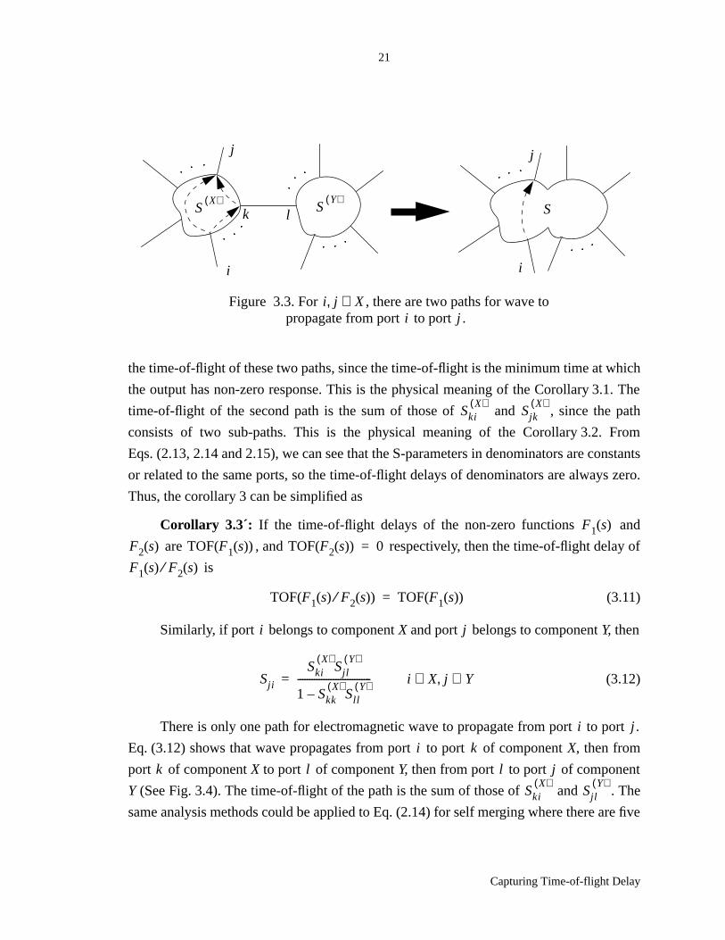
Figure 3.3. For , there are two paths for wave to propagate
from port to port .. . . . . . . . . . . . . . . . . . . . . . . . . . . . . . . . . . . . . . . . . . . . . . . 21
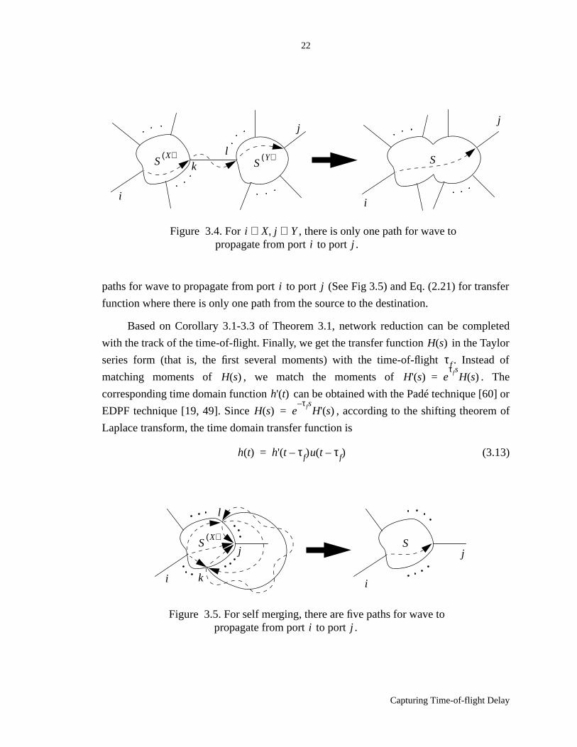
Figure 3.4. For , there is only one path for wave to propagate
from port to port .. . . . . . . . . . . . . . . . . . . . . . . . . . . . . . . . . . . . . . . . . . . . . . . 22
Figure 3.5. For , there are two paths for wave to propagate
from port to port .. . . . . . . . . . . . . . . . . . . . . . . . . . . . . . . . . . . . . . . . . . . . . . . 22
Figure 4.1. An RC circuit with floating capacitance loops.. . . . . . . . . . . . . . . . . . . . . . 30
Figure 4.2. Output response of the RC circuit. . . . . . . . . . . . . . . . . . . . . . . . . . . . . . . . 30
Figure 4.3. The responses of the RLC circuit. . . . . . . . . . . . . . . . . . . . . . . . . . . . . . . . . 31
Figure 4.4. A clock network. . . . . . . . . . . . . . . . . . . . . . . . . . . . . . . . . . . . . . . . . . . . . . 32
Figure 4.5. Output response at node U1. . . . . . . . . . . . . . . . . . . . . . . . . . . . . . . . . . . . . 32
Figure 4.6. MCMC-93 benchmark. . . . . . . . . . . . . . . . . . . . . . . . . . . . . . . . . . . . . . . . . 33
Figure 4.7. The result comparison of the MCMC-93 benchmark by SPICE3e2
and the 5th order approximation without time-of-flight extraction (nonTOF). . . 34
Figure 4.8. The result comparison of the MCMC-93 benchmark by SPICE3e2
and the 5th order approximation with time-of-flight extraction (TOF). . . . . . . . . 34
Figure 4.9. A transmission line circuit. . . . . . . . . . . . . . . . . . . . . . . . . . . . . . . . . . . . . . 35
Figure 4.10. The result comparison of the lossy line circuit by SPICE3e2 and
i j X∈,i j
i X j Y∈,∈i j
i j X∈,i j
vi
the 4th order approximation without time-of-flight extraction (nonTOF).. . . . . . 35
Figure 4.11. The comparison of the lossy line circuit by SPICE3e2 and
the 4th order approximation with time-of-flight extraction (TOF). . . . . . . . . . . . 36
Figure 5.1. Macromodel with virtual nodes. . . . . . . . . . . . . . . . . . . . . . . . . . . . . . . . . . 39
Figure 5.2. Equivalent circuit of a two port macromodel.. . . . . . . . . . . . . . . . . . . . . . . 41
Figure 5.3. A lossy transmission line circuit with nonlinear loads.. . . . . . . . . . . . . . . . 42
Figure 5.4. Near end response of the lossy transmission line circuit. . . . . . . . . . . . . . . 43
Figure 5.5. Far end response of the lossy transmission line circuit. . . . . . . . . . . . . . . . 43
Figure 5.6. Grid-type clock network.. . . . . . . . . . . . . . . . . . . . . . . . . . . . . . . . . . . . . . . 44
Figure 5.7. Near end response of the clock network.. . . . . . . . . . . . . . . . . . . . . . . . . . . 45
Figure 5.8. Far end response of the clock network.. . . . . . . . . . . . . . . . . . . . . . . . . . . . 45
Figure 5.9. Comparison of different order approximation. . . . . . . . . . . . . . . . . . . . . . . 46
Figure 6.1. Several smaller components are more efficient
than one large component to model complex interconnects. . . . . . . . . . . . . . . . . 48
Figure 6.2. Bucket list structure. . . . . . . . . . . . . . . . . . . . . . . . . . . . . . . . . . . . . . . . . . . 50
Figure 7.1. Circuit models between pairs of ports. . . . . . . . . . . . . . . . . . . . . . . . . . . . . 53
Figure 7.2. RC parallel model of a port. . . . . . . . . . . . . . . . . . . . . . . . . . . . . . . . . . . . . 55
Figure 7.3. Number of the reduced circuit elements versus number of ports.. . . . . . . . 59
Figure 7.4. Simulation time of the reduced circuits versus number of ports. . . . . . . . . 59
Figure 7.5. Simulation results of the clock network. . . . . . . . . . . . . . . . . . . . . . . . . . . . 60
Figure 7.6. A clock network with nonlinear drivers and loads.. . . . . . . . . . . . . . . . . . . 61
Figure 7.7 Comparison of results of the clock network system
and its equivalent circuit . . . . . . . . . . . . . . . . . . . . . . . . . . . . . . . . . . . . . . . . . . . . 61
Figure 8.1. Input voltage transition and the current source model. . . . . . . . . . . . . . . . . 64
Figure 8.2. pMOS current when . . . . . . . . . . . . . . . . . . . . . . . . . . . . . . . . . . . . . 66
Figure 8.3. pMOS current and nMOS current (leakage current) . . . . . . . . . . . . . . 73
tpl tr<
ip in

vii
Figure 8.4. An RC circuit with floating capacitors. . . . . . . . . . . . . . . . . . . . . . . . . . . . . 75
Figure 8.5. Voltage response of the RC circuit. . . . . . . . . . . . . . . . . . . . . . . . . . . . . . . . 76
Figure 8.6. A grid-type clock network. . . . . . . . . . . . . . . . . . . . . . . . . . . . . . . . . . . . . . 76
Figure 8.7. Voltage response of the clock network.. . . . . . . . . . . . . . . . . . . . . . . . . . . . 77
Figure 8.8. A transmission line circuit with a DC path from source to ground. . . . . . . 77
Figure 8.9. pMOS and nMOS currents of the transmission line circuit. . . . . . . . . . . . . 78
Figure 8.10. Voltage response of the transmission line circuit. . . . . . . . . . . . . . . . . . . . 78
Figure 8.11. Voltage response of a large clock network. . . . . . . . . . . . . . . . . . . . . . . . . 79
Figure A.1. An ideal interconnect node. . . . . . . . . . . . . . . . . . . . . . . . . . . . . . . . . . . . . 83

viii
List of Tables
Table 5.1. Comparison of the macromodel and TIM. . . . . . . . . . . . . . . . . . . . . . . . . . . 46
Table 7.1. The clock network reduction for different number of ports . . . . . . . . . . . . . 58
Table 7.2. The loop circuit and the mesh circuit reduction results . . . . . . . . . . . . . . . . 60

Scattering-Parameter-Based Macromodelfor Transient Analysis of Interconnect Networks with
Nonlinear Terminations
Haifang Liao
ABSTRACT
An efficient method for analyzing general distributed-lumped interconnect networks
with linear or nonlinear loads for transient simulation is presented. The method is based
on scattering parameter techniques. The reduced-order approximate models of linear
networks with multiple inputs and outputs can be obtained in one pass of reduction. Only
two operations are used to do circuit reduction. The circuit partition is efficiently
combined with the circuit reduction process to speed up the reduction process, decrease
the simulation time and achieve the high accuracy using lower order approximation. The
partition is very suitable for large interconnect networks with large number of external
ports. For transmission line networks, we can easily capture time-of-flight delay explicitly
during the reduction, which greatly improves the accuracy of the macromodel. Mixed
Exponential Functions (MEFs) are used to approximate the scattering parameters of the
macromodel. MEF preserves the high accuracy of Padé approximation and yield a
guaranteed stable solution. With recursive convolution formulas, the macromodel has
been integrated into SPICE-like simulators. The interconnect networks with nonlinear
terminations also can be analyzed by replacing the linear parts with lower order equivalent
circuits. We developed a practical circuit reduction method to reduce large RC
interconnect networks into lower order equivalent RC circuits. In conjunction with the
macromodel with explicit convolution formulas, a CMOS driver model is also presented
for the transient analysis and power dissipation analysis. The model takes into account the
input slope effects, CMOS nonlinear effects and load interconnect effects. The
macromodel and the driver model provide accuracy comparable to that of SPICE, with
one or two orders of magnitude less computing time.
Keywords: macromodel, scattering parameter, circuit reduction, circuit partition,
circuit synthesis, time-of-flight, recursive convolution, transmission line, CMOS driver
model, transient analysis, timing analysis, power dissipation analysis.

x
Acknowledgment
I would like to thank Professor Wayne Dai, my advisor, for his guidance,
encouragement, enthusiasm and unceasing support throughout the course of my degree
study. His insights and suggestions have given me an enormous amount of help in
pursuing this research. I want to thank Professor Pak Chan and Professor Patrick Mantey
for reviewing this thesis and giving very helpful suggestions. Many thanks also to all
members of our research group, but particularly, Jimmy Wang for his suggestion regarding
capturing of time-of-flight delay of transmission line networks.
I would like to thank Dr. Rui Wang of Intel for many useful discussion at the early
stage of this research, Dr. Peter Saviz of Intel and Dr. Norman Chang of HP for providing
industry circuits and their help to integrate the macromodel into Intel and HP internal
simulators, and Zhong L. Mo of EPIC and John Chow of Archer for providing testing
benchmarks and evaluating simulation results. I also like to thank Professor Andrew Yang
of University of Washington for providing their Model Independent SIMulator (MISIM).
Mostly, I would like to thank my wife, Yanhua, for her discussion, understanding,
tolerance and much needed encouragement, and my daughter, Celina, who more than
anyone inspired me to finish this work.

1
Introduction
CHAPTER 1 Introduction
As circuit switching speed increases, the interconnect behavior has become the main
factor to impose limitations on high performance systems. However, detailed analyses of
interconnects are usually computationally expensive due to the distributed and dispersive
nature of the network. To extract accurately the interconnect networks, the large number
of internal nodes or circuit elements can overwhelm any circuit simulator. But the detailed
inner working of these nodes are usually of little interests to the system designer and,
therefore, need not be explicitly represented into computational models. In Chapter 2, we
introduce a scattering-parameter-based macromodel of distributed-lumped networks.
Scattering parameters are well suited for the characterizing and modeling of linear high
frequency devices. The scattering parameters of passive elements always have an absolute
values less than one. This dramatically increases the numerical stability of the algorithm.
They are also easier to directly measure on broad frequency bands [36]. By introducing a
special circuit component called “multiport interconnect node” [46], an efficient network
reduction algorithm is developed to reduce the original network into a network containing
one multiport component (macromodel) together with sources and loads of interest, which
may be nonlinear [48, 49, 51]. The method can handle general RLC and transmission line
networks including capacitive or inductive cutsets and loops. Unlike the method in [41]
where system admittance matrix is computed one column at a time, our method computes
the system matrix in one pass of reduction.
When the electrical length of interconnects becomes a significant fraction of signal
wavelength during the fast transient, the conventional lumped-impedance interconnect

2
Introduction
model becomes inadequate and transmission line effects must be taken into account for
both on-chip and off-chip interconnects. The delay associated with transmission line
networks consists of the exponentially charging time and a pure propagation delay
representing the finite propagating speed of electromagnetic signals in the dielectric
medium. This propagation delay, so called “time-of-flight delay”, is particularly evident in
long lines. As the time-of-flight of the signal across the interconnect is greater than, or
comparable to, the input signal rise-time (i.e. long interconnects), it is most difficult to
capture the time-of-flight delay with a finite order approximation [80, 83], whether a finite
sum of exponentials[9, 54] or an exponentially decayed polynomial function [19, 49].
Hence, the time-of-flight must be captured explicitly from the transfer function of the
circuit. While finding the explicit analytical expression of the transfer function for an
arbitrary interconnect system to compute the time-of-flight is impractical, several attempts
have been made by others to extract the time-of-flight delay. They either require an
explicit analytical expression of the transfer function [18] or can only deal with one set of
transmission lines [54, 10]. The extracted time-of-flight of one transmission line is also
used as the lower bound of the delay for the lossy transmission lines [80, 83]. In
Chapter 3, we present a new method based on a scattering-parameter-macromodel to
compute the time-of-flight for arbitrary interconnect systems, not limited to one
transmission line [52]. The accuracy of output responses, due to the extraction of the time-
of-flight, is greatly improved.
While integrating transmission line simulation in a transient circuit simulator, the
fundamental difficulty arises because the circuits containing nonlinear devices must be
characterized in the time domain while transmission lines with loss, dispersion, and
interconnect discontinuities are best modeled in the frequency domain. To cope with this
difficulty, direct convolution techniques are used. The system outputs are the convolutions
of the inputs with the impulse responses. While explicit analytical expression of the
impulse responses is impractical, the numerical inverse Fast Fourier Transformation
technique suffers from the fact that excessive number of frequency points are needed to
avoid aliasing effects. Another drawback of the direct convolution is the computing time it
consumes.
In order to deal with these difficulties, Padé technique is used to get an approximated
explicit analytical expression of the transfer function [60, 54, 21, 48, 64]. Impulse
response functions are approximated with a sum of exponential functions in time domain.
3
Introduction
However, the Padé technique suffers from the instability problem: unstable poles may be
generated for known stable networks [16]. Instead of using Padé technique, based on the
method of inversion of Laplace transform, F. Y. Chang [19] introduced Laguerre functions
(or Exponentially-Decayed Polynomial Functions) to approximate the impulse response
functions, together with a recursive convolution formula. But the accuracy of the Laguerre
approximation is very sensitive to the time constant, which is chosen based on a very
rough empirical formula. In Chapter 4, we propose an improved method to choose the
time constant by introducing an error function [49]. The further improvement has been
done by introducing a Mixed-Exponential Function (MEF) [51] which takes advantage of
the best properties of Padé approximation and Exponentially-Decayed Polynomial
Function (EDPF), this method efficiently achieves the high accuracy afforded by the
former, and high stability by the latter. Furthermore, when the macromodel is incorporated
into a SPICE-like simulator, more constraints must be imposed on the macromodel. The
moment matching techniques including Padé approximation and EDPF approximation
may create a non-positive real Y-matrix (or equivalently non-bounded real S-matrix). The
positive-real Y-matrix (or bounded real S-matrix) is the necessary and sufficient condition
for the corresponding network to be passive [40]. A non-positive-real Y-matrix may result
in unstable simulation. A practical testing method is introduced in Chapter 5.
To avoid folding, sliding, multiplication, and integration in the progressively time-
consuming direct convolution integration process for incorporating the macromodel into
SPICE-like simulators, the recursive formula [73] is rediscovered [54, 64] for computing
convolution of exponential function with any other function. A recursive convolution
formula of exponential decayed polynomial function with any other function is also
derived by F. Y. Chang [19]. In Chapter 5, we simplify recursive convolution formula
[50], and derive the Norton equivalent circuit of the macromodel to handle nonlinear
terminations. This macromodel has been incorporated into MISIM [82], the Intel internal
simulator TIM and the HP internal simulator HSPICE, with a simplified recursive
convolution formula [50].
The macromodels generated by moment matching technique are the approximation
of the port behavior of the interconnects. In order to incorporate the macromodels into
SPICE-like simulator, they are usually described by an admittance matrix (Y-matrix) [64,
40]. The Y-matrices are generally full matrices. When the number of external ports of an
interconnect network is large, the number of entries of the matrix may be larger than the

4
Introduction
number of circuit elements of the original interconnect network. For example, a clock
network with 500 fanouts will create more than 250,000 entries of the corresponding Y-
matrix. This huge full matrix may even increase the computational burden of traditional
SPICE simulation. On the other hand, trying to model the huge full matrix by lower order
approximation with moment matching techniques is impractical. Severe numerical
problems may result in extremely ill-conditioned matrices for computing high order
moments. The “complex-frequency hopping” method [22] and the PVL (Padé
approximation via the Lanczos process) [29] make great efforts to compute high order
moments by avoiding the ill-conditioning problem. However, increasing the
approximation order will increase the modeling and simulation time. There is no efficient
method to obtain the reduced-order approximate models of linear networks, especially
when a large circuit with large number of ports is terminated with nonlinear drivers and
loads,. The difficulty of reducing a large linear network with large number of ports can be
dealt with by partitioning the network into smaller subnetworks. A linear time algorithm is
proposed in Chapter 6 to partition a large interconnect network into subnetworks. Each of
them can be approximated with a lower-order model. Circuit partitioning speeds up the
reduction process, decreases the simulation time and achieves the high accuracy using
lower order approximation. The accuracy is controlled by adjusting the number of circuit
elements in each subnetwork. The circuit partitioning provides a feasible and efficient way
to handle large circuits with large number of external ports.
A new strategy to analyze large interconnect circuits with nonlinear terminations is
to synthesize the interconnect networks with lower-order equivalent circuits. A circuit
synthesis method based on moment matching technique is presented in Chapter 7 to
generated RC interconnects. Since the resistance and capacitance of the synthesized
circuits are positive, the circuits are always stable. The reduced circuits can be simulated
using existing circuit simulators without modification.
Despite the increasing importance of interconnects in transient analysis, nonlinear
active devices in a system also contribute to the system behavior significantly. A new
CMOS driver model is proposed in Chapter 8 to be used in conjunction with the
macromodel of interconnect networks for transient and power dissipation analysis. This
model considers the input slope effects, CMOS nonlinear effects and load interconnect
effects. The driver output current is represented by a linear-quadratic-exponential
piecewise model. Based on this model, we can accurately evaluate the CMOS transient
5
Introduction
leakage (short-circuit) current and short-circuit power dissipation.
Overall, the main contributions of this research include
• Development of an efficient network reduction method to reduce general
interconnect networks into a macromodel.
• Specification of a precise definition of time-of-flight and creation of a lower
order computational model of general interconnect systems keeping the track
of time-of-flight delay, which greatly improve the macromodels of
transmission line networks.
• The improved Exponential Decayed Polynomial Function approximation
obtained by choosing the optimal time constant, and a proposed Mixed-
Exponential Function to approximate the higher order circuit systems.
• Simplification of the formula of recursive convolution with exponential
decayed polynomial function and derivation of a Norton equivalent circuit to
incorporate the macromodel into SPICE-like simulator.
• Development of a linear time partitioning algorithm and efficiently combine
the partitioning with reduction process, which is very efficient to analyze large
networks with large number of eternal ports.
• Synthesis of multiport interconnect networks without transformers. Complex
networks are approximated with lower order equivalent circuits, and the
equivalent circuits are always stable.
• Creation of a new CMOS driver model which can be used in conjunction with
interconnect macromodel. Leakage current and power dissipation can be
analyzed.

6
Scattering-Parameter-Based Macromodel
CHAPTER 2 Scattering-Parameter-BasedMacromodel
Linear high speed interconnect networks have been studied quite extensively [15,
19, 22, 54, 60, 69] because of the ever increasing demand of high performance systems.
Detailed analyses of interconnects are usually computationally expensive due to the
distributed and dispersive nature of the network. To extract accurately the interconnect
networks, the large number of internal nodes or circuit elements can overwhelm any
circuit simulator. However, the detailed inner working of these nodes are usually of little
interests to the system designer and, therefore, need not be explicitly represented into
computational models. In this chapter, we introduce a scattering-parameter-based
macromodel of distributed-lumped networks. By introducing a special circuit component
called multiport interconnect node [46], an efficient network reduction algorithm with
only two merging rules is developed to reduce the original network into a network
containing one multiport component (macromodel) together with sources and loads of
interest, which may be nonlinear [48, 49, 51]. The method can handle general RLC and
transmission line networks including capacitive or inductive cutsets and loops. Unlike the
method in [41] where system admittance matrix is computed one column at a time, our
method computes the system matrix in one pass of reduction.
2.1 Scattering Parameters of Distributed-Lumped Components
We use scattering parameters (S-parameters) to describe the components of

7
Scattering-Parameter-Based Macromodel
interconnect systems. Scattering parameters are a powerful way to describe and model
interconnects. They can be measured directly at high frequencies and they exists for all
distributed-lumped circuit elements including open and short circuits. They can also
describe transmission lines which is critical in today’s high-speed designs. A scattering
matrix is employed to relate outgoing waves to incoming waves of a multiport [26]. For an
port component, the scattering matrix of the component can be defined as
(2.1)
where is the complex frequency, and are the incoming voltage wave at port and
the outgoing wave at port , respectively. The wave parameters and have a clear and
definite relationship with circuit parameters. Let and be voltage and current
respectively at port . Then they are related
and (2.2)
where is the reference impedance. Eqs. (2.1) and (2.2) can be used to derive scattering
parameters of some basic components.
The components utilized to characterize a general interconnect network can be
classified into four types [49]: 1) one-port impedance, 2) two-port impedance, 3) lossy
transmission line and 4) multiport interconnect node (See Fig. 2.1). The scattering
parameters of the first three components can be derived as follows [26]:
For the one port element in Fig. 2.1(a), . Considering Eq. (2.2), we have
n
Sji s( )bj
ai----
ak 0= k i≠,= i j, 1 2 … n, , ,=
s ai bj i
j ai bi
Vi I i
i
ai bi+ Vi= ai bi– Z0I i=
Z0
Figure 2.1. Four basic elements.
1
2 3
n
Z
Z
(a) One-port impedance (b) Two-port impedance
(d) Multiport interconnect node(c) Lossy transmission line
V ZI=
8
Scattering-Parameter-Based Macromodel
(2.3)
Thus,
(2.4)
For the two-port, according to Kirchoff’s voltage law and current law,
(2.5)
Transferring the circuit parameters to wave parameters with Eq. (2.2),
(2.6)
and solving the above equation, we have
(2.7)
where S-matrix
(2.8)
For an RLC transmission line, the telegrapher’s equations are
(2.9)
where , and are per-unit-length resistance, inductance and capacitance,
respectively. is the distance from the left end of the transmission line. For the line with
length , the solution of Eq. (2.9), with boundary conditions of ( ) and ( ) at
two ends of the line respectively, is
a b+ Z a b–( ) Z0⁄=
Sba---
Z Z0–
Z Z0+---------------= =
V1 ZI1 V2+=
I1 I2+ 0=
a1 b1+ Z a1 b1–( ) Z0⁄ a2 b2+ +=
a1 b1– a2 b2–+ 0=
b1
b2
Sa1
a2
=
S1
Z 2Z0+------------------
Z 2Z0
2Z0 Z=
x∂∂
V s x,( ) sL R+( )–=
x∂∂
I s x,( ) sC–=
R L C
x
l V1 I1, V2 I2,

9
Scattering-Parameter-Based Macromodel
(2.10)
where is the characteristic impedance, is the
propagation constant. Combining Eq. (2.2) and (2.10), we obtain the S-matrix of the lossy
transmission line,
(2.11)
The interconnect topology as shown in Fig. 2.1(d) can be used to connect
components described in Fig. 2.1(a) through Fig. 2.1(c) to construct a generalized
interconnection network. The port interconnect node can also be described by the
scattering matrix [46]:
(2.12)
(Please see Appendix A for the detailed derivation). Combining these four basic
elements and all multiport elements described by S-parameters, one can represent a
variety of distributed-lumped network topology including capacitive cutsets, inductive
loops, and lossy transmission lines.
2.2 Scattering-Parameter-Based Macromodel
Given the individual component scattering parameters, we describe a systematic
reduction algorithm to reduce a distributed-lumped network to a multiport with sources
and loads of interest.
The network reduction problem can be defined as follows[48, 49]: given a linear
distributed-lumped network described by S-parameters, find a multiport representation of
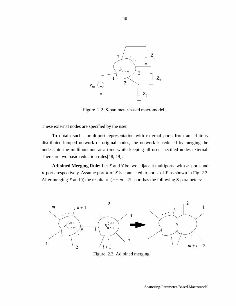
the network as illustrated in Fig. 2.2., where the multiport is characterized by its S-
parameters. All nodes in the network are internal to the multiport except the node
connected to the driving source (node ) and the loads of interest (nodes through ).
I1
I2
1Zc----- γl( )coth γl( )csch–
γl( )csch– γl( )coth
V1
V2
=
Zc R sL+( ) sC⁄= γ R sL+( ) sCl=
S1
2Z0Zc γ( )cosh Zc2
Z02
+( ) γ( )sinh+----------------------------------------------------------------------------------------
Zc2
Z02
–( ) γ( )sinh 2ZcZ0
2ZcZ0 Zc2
Z02
–( ) γ( )sinh=
n
S1n---
2 n– 2 … 2
2 2 n– … 2
… … … …2 2 … 2 n–
=
1 2 n
10
Scattering-Parameter-Based Macromodel
These external nodes are specified by the user.
To obtain such a multiport representation with external ports from an arbitrary
distributed-lumped network of original nodes, the network is reduced by merging the
nodes into the multiport one at a time while keeping all user specified nodes external.
There are two basic reduction rules[48, 49]:
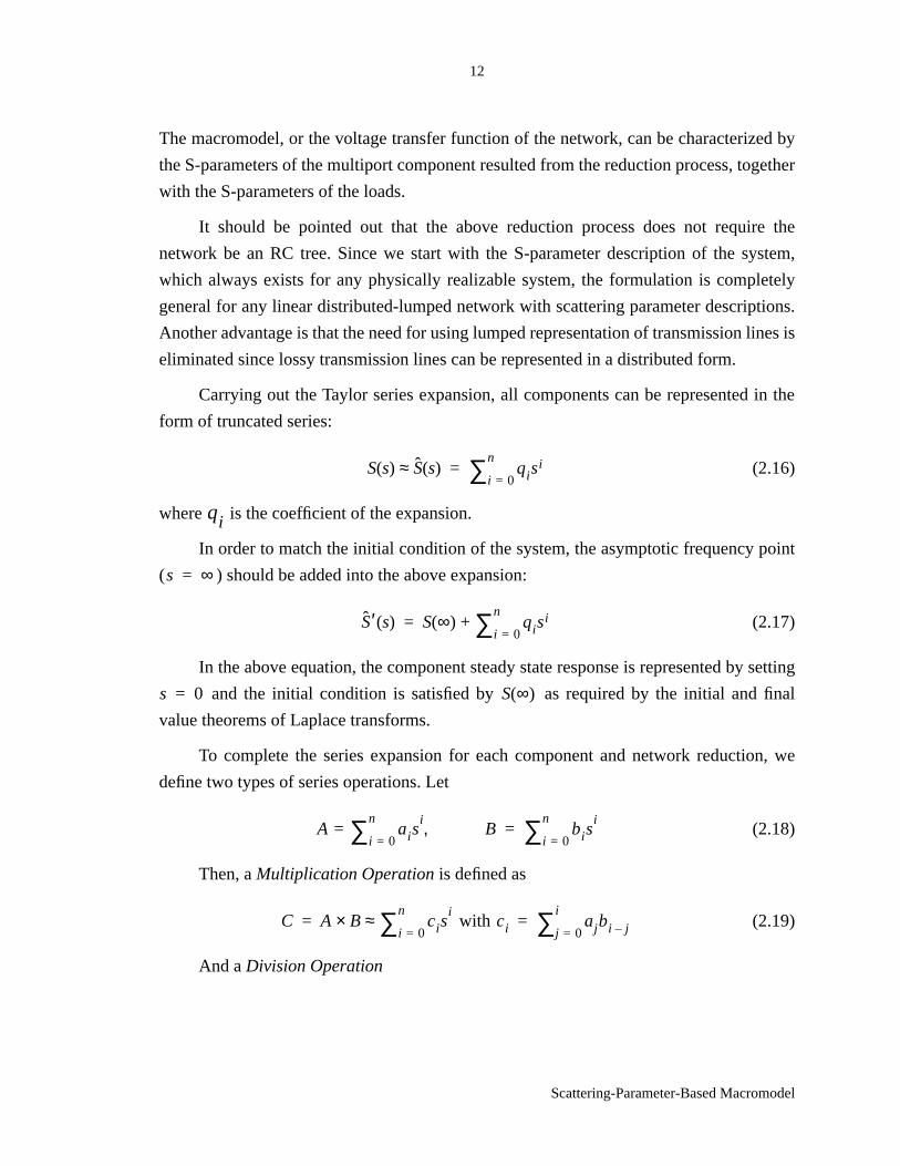
Adjoined Merging Rule: Let X andY be two adjacent multiports, with ports and
ports respectively. Assume port ofX is connected to port ofY, as shown in Fig. 2.3.
After mergingX andY, the resultant port has the following S-parameters:
Figure 2.2. S-parameter-based macromodel.
2vin
1
n Zn
Z2
Sn n×
Z3
3
m
n k l
Figure 2.3. Adjoined merging.
Sn n×Y( )
k l
12
k 1+m
1
2
l 1+
n
Sm m×X( )
12
m n 2–+
S
n m 2–+( )

11
Scattering-Parameter-Based Macromodel
(2.13)
Self Merging Rule: Let X be an port with a self loop connected to port and , as
shown in Fig. 2.4. After eliminating the self loop, the resultant port has the
following S-parameters:
(2.14)
where
(2.15)
For an arbitrary distributed-lumped network described by the linear components, the
Adjoined Merging Rule is used to merge all internal components, and the Self Merging
Rule is applied to eliminate the self loops introduced by the Adjoined Merging process.
Sji
SjiX( ) Ski
X( )Sll
Y( )Sjk
X( )
1 SkkX( )
SllY( )
–---------------------------------+ i j X∈,
SjiY( ) Sli
Y( )Skk
X( )Sjl
Y( )
1 SkkX( )
SllY( )
–---------------------------------+ i j Y∈,
SkiX( )
SjlY( )
1 SkkX( )
SllY( )
–------------------------------- i X j Y∈,∈
=
m l k
Figure 2.4. Self merging.
S
m 2–
1
k 1+
l
k
m
1
Sm m×X( )
m 2–( )
Sji SjiX( )
SjlX( )
al SjkX( )
ak i j, 1 2 … m, , 2–,=+ +=
al1∆--- Sli
X( )Skk
X( )Ski
X( )1 Slk
X( )–( )+( )=
ak1∆--- Ski
X( )Sll
X( )Sli
X( )1 Skl
X( )–( )+( )=
∆ 1 SlkX( )
–( ) 1 SklX( )
–( ) SllX( )
SkkX( )
–=
12
Scattering-Parameter-Based Macromodel
The macromodel, or the voltage transfer function of the network, can be characterized by
the S-parameters of the multiport component resulted from the reduction process, together
with the S-parameters of the loads.
It should be pointed out that the above reduction process does not require the
network be an RC tree. Since we start with the S-parameter description of the system,
which always exists for any physically realizable system, the formulation is completely
general for any linear distributed-lumped network with scattering parameter descriptions.
Another advantage is that the need for using lumped representation of transmission lines is
eliminated since lossy transmission lines can be represented in a distributed form.
Carrying out the Taylor series expansion, all components can be represented in the
form of truncated series:
(2.16)
where is the coefficient of the expansion.
In order to match the initial condition of the system, the asymptotic frequency point
( ) should be added into the above expansion:
(2.17)
In the above equation, the component steady state response is represented by setting
and the initial condition is satisfied by as required by the initial and final
value theorems of Laplace transforms.
To complete the series expansion for each component and network reduction, we
define two types of series operations. Let
(2.18)
Then, aMultiplication Operation is defined as
with (2.19)
And aDivision Operation
S s( ) S s( )≈ qisi
i 0=
n∑=
qi
s ∞=
S′ s( ) S ∞( ) qisi
i 0=
n∑+=
s 0= S ∞( )
A aisi
i 0=
n∑= , B bisi
i 0=
n∑=
C A B× cisi
i 0=
n∑≈= ci ajbi j–j 0=
i∑=
13
Scattering-Parameter-Based Macromodel
with (2.20)
From Eq. (2.20), it seems that a negative first moment would be created if
. This case may happen when using admittance matrix or state equations.
However, since we use scattering parameters to characterize all components, all scattering
parameters of passive components have no poles at based on the principle of
energy conservation [67]. Therefore, if represents an element of a scattering matrix, it
is guaranteed that there is no pole at . This implies that if , must be zero,
so we can shift all moments of and to the left and keep .
Several network reduction algorithms have been reported. The multiport connection
method was introduced in [26, 34, 57]. In this method, the scattering-matrix of the
network is partitioned into blocks based on classification of internal and external ports.
The scattering-matrix can be obtained using block operations including time-consuming
matrix inversion. Connecting two multiports at a time from bottom up may reduce the
computation time. However, matrix inversion is still unavoidable. Kuhn [43] introduced a
flow graph reduction method. A microwave network is represented by a flow graph and
the graph can be reduced step-by-step based on four reduction rules. This method,
however, has not been widely used because of its complexity with large networks. Here,
we introduce two simple rules for fast network reduction. While Kuhn reduces the
network one branch at a time, we reduce the network one node at a time. Unlike the
previous approaches, our method approximates S-parameter by expanding them into
Taylor series and reduces networks with series operations, which further improves the
efficiency of our reduction process. In a later section, we will show the approximation is
accurate for delay computation.
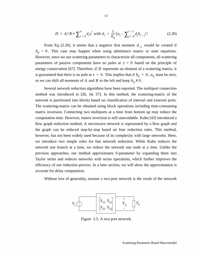
Without loss of generality, assume a two-port network is the result of the network
D A B⁄ disi
i 0=
n∑≈= di1b0----- ai djbi j–j 0=
i 1–∑–( )=
d 1–
b0 0=
s 0=
D
s 0= b0 0= a0
A B b0 0≠
Figure 2.5. A two port network.
S11 S12
S21 S22
ViVo
So
14
Scattering-Parameter-Based Macromodel
reduction process (See Fig. 2.5). The the voltage transfer function of the network can be
characterized by the S-parameters of the multiport component resulted from the reduction
process, together with the S-parameters of the loads. From this reduced network, we can
easily get the transfer function.
(2.21)
where is the S-parameter of the load.
H s( )S21 1 So+( )
1 S11 So S12S21 S11S22– S22–( )+ +---------------------------------------------------------------------------------------=
So
15
Capturing Time-of-flight Delay
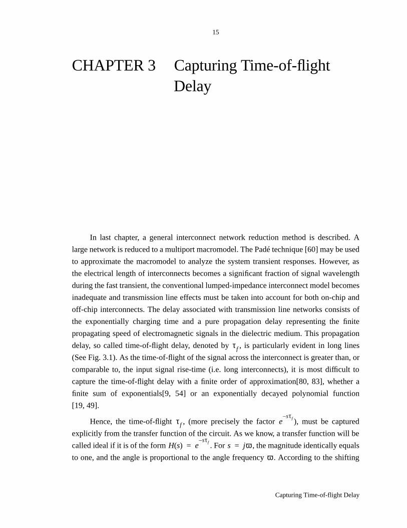
CHAPTER 3 Capturing Time-of-flightDelay
In last chapter, a general interconnect network reduction method is described. A
large network is reduced to a multiport macromodel. The Padé technique [60] may be used
to approximate the macromodel to analyze the system transient responses. However, as
the electrical length of interconnects becomes a significant fraction of signal wavelength
during the fast transient, the conventional lumped-impedance interconnect model becomes
inadequate and transmission line effects must be taken into account for both on-chip and
off-chip interconnects. The delay associated with transmission line networks consists of
the exponentially charging time and a pure propagation delay representing the finite
propagating speed of electromagnetic signals in the dielectric medium. This propagation
delay, so called time-of-flight delay, denoted by , is particularly evident in long lines
(See Fig. 3.1). As the time-of-flight of the signal across the interconnect is greater than, or
comparable to, the input signal rise-time (i.e. long interconnects), it is most difficult to
capture the time-of-flight delay with a finite order of approximation[80, 83], whether a
finite sum of exponentials[9, 54] or an exponentially decayed polynomial function
[19, 49].
Hence, the time-of-flight , (more precisely the factor ), must be captured
explicitly from the transfer function of the circuit. As we know, a transfer function will be
called ideal if it is of the form . For , the magnitude identically equals
to one, and the angle is proportional to the angle frequency . According to the shifting
τf
τf esτf–
H s( ) esτf–
= s jω=
ω

16
Capturing Time-of-flight Delay
theorem of Laplace transform, if this ideal network is excited by a signal , the
corresponding response of the network will be . The response is the same as the
excitation except that it is delayed in time by an amount . That is, the response for
is equal to zero. Therefore, the time-of-flight is defined as the maximum delay during
which the output response is zero for any finite input. The corresponding factor in the
frequency domain is .
While finding the explicit analytical expression of the transfer function for an
arbitrary interconnect system to compute the time-of-flight is impractical, several attempts
have been made to extract the time-of-flight delay. They either require an explicit
analytical expression of the transfer function[18] or can only deal with one set of
transmission lines[54, 10]. The extracted time-of-flight of one transmission line is also
used as the lower bound of the delay for the lossy transmission lines[80, 83].
Here, we present a new method to compute the time-of-flight for arbitrary
interconnect systems, not limited to one transmission line [52]. The method is based on a
scattering-parameter-macromodel described in last Section. The accuracy of output
responses, due to the extraction of the time-of-flight, is greatly improved.
3.1 Properties of Time-of-Flight
Recall that the time-of-flight is the maximum delay during which the output
response is zero for a finite input signal. The computation can be approached from the
properties of transfer function in the frequency domain. The following theorem is useful
τf
Figure 3.1. Time-of-flight delay .τf
Output
Input
e t( )
e t τf–( )
τf t τf<
esτf–

17
Capturing Time-of-flight Delay
to capture the time-of-flight for the transfer function .
Theorem 3.1:For any , there exists positive constant , such that the time-of-
flight of the transfer function satisfies the following
for all (3.1)
Proof: Let be a finite input signal, and be its Laplace transform.
According to the initial value theorem of Laplace transform, .
From the definition of the time-of-flight, the corresponding time domain response
is zero for . According to the shifting theorem, the Laplace transform of the
function is
Obviously, is finite for any passive networks when the input is finite. Now, let
us prove Eq. (3.1) by contradiction. First, assume that there exists such that
for all , then
This contradicts the fact that is a finite value. Thus, is held.
On the other hand, assume that there exists such that for all
, then the initial value of the function for some positive
is
H s( )
ε 0> s0
τf H s( )
eεs–
H s( ) eτfs e
εs< < s s0≥
vi t( ) Vi s( )
ss ∞→lim Vi s( ) vi 0
+( )=
vo t( ) t τf<vo t( ) vo t τf+( )=
Vo s( ) eτfsVo s( )=
eτfsH s( )Vi s( )=
vo 0+
( )
ε 0>H s( ) e
τfs eεs≥ s s0≥
vo 0+
( ) ss ∞→lim Vo s( )=
ss ∞→lim e
τfs H s( ) Vi s( )=
vi 0+
( ) eτfs H s( )
s ∞→lim=
vi 0+
( ) eεs
s ∞→lim ∞→≥
vo 0+
( ) H s( ) eτfs e
εs<
ε 0> eεs–
H s( ) eτfs≥s s0≥ vo t( ) vo t τf σ+ +( )= σ ε<

18
Capturing Time-of-flight Delay
That is, the output response is still zero at for any finite input
signal. This contradicts the definition: the time-of-flight is the maximum delay during
which the output response is zero for a finite input signal. Thus is held.
Notice that the definition of time-of-flight in [6], referred by others (e.g. in [18]), is
(3.2)
This definition may be incorrect for some special cases. For example, the transfer
function of the transmission line circuit shown in Fig. 3.2 is
(3.3)
where and . Obviously, its time-of-flight is
according to the above theorem. This can also be easily verified because of
the speed of electromagnetic wave is . But according to Eq. (3.2), it is zero.
Theorem 3.1 gives a precise description of time-of-flight. But it is difficult to
compute the time-of-flight for a large network directly based on the theorem since it is
vo 0+
( ) ss ∞→lim Vo s( )=
ss ∞→lim e
τf σ+( ) sH s( ) Vi s( )=
vi 0+
( ) eτf σ+( ) s
H s( )s ∞→lim=
vi 0+
( ) eσ ε–( ) s
s ∞→lim 0→≤
vo t( ) t τf σ+=
H s( ) eτfs e
εs–>
τf12---–
s ∞→lim
sdd
lnH s( )H s–( )-------------=
vo
R L C, ,
ZN
ZN
l
Figure 3.2. Transmission line circuit.
vin
H s( )2ZNZc
ZN Zc+( ) 2e
γZN Zc–( ) 2
eγ–
–-------------------------------------------------------------------------=
Zc R sL+( ) sC( )⁄= γ R sL+( ) sCl=
τf LCl=
1 LC⁄

19
Capturing Time-of-flight Delay
impractical to get an explicit expression of the transfer function. To cope this problem, we
introduce following three corollaries.
Corollary 3.1: If the time-of-flight delays of non-zero functions and are
, and respectively, then the time-of-flight delay of
is
(3.4)
Corollary 3.2: If the time-of-flight delays of non-zero functions and are
, and respectively, then the time-of-flight delay of is
(3.5)
Corollary 3.3: If the time-of-flight delays of non-zero functions and are
, and respectively, then the time-of-flight delay of is
(3.6)
Above corollaries can be easily proved according to the Theorem 3.1. These results
will be used later to keep track of the time-of-flight during the network reduction. Later
we will show that these corollaries have clear physical meaning during network reduction.
Let us first describe the time-of-flight delays of scattering parameters of basic circuit
components.
3.2 Scattering Parameters of Components with Time-of-Flight Captured
In order to extract time-of-flight delays s of interconnect systems, let us review the
four basic circuit elements shown in Fig. 2.1. Their S-parameter are expressed in Eqs.
(2.4-2.12). In these four basic elements, the one-port impedance, the two-port impedance
and multiport interconnect node are all lumped components, i.e., electromagnetic waves
propagate across the component virtually instantaneously. Therefore, the time-of-flight
delays of S-parameters described in Eqs. (2.4, 2.8, 2.12) are all equal to zero.
Applying Theorem 3.1 to the S-matrix of the lossy transmission line (See Eq.
(2.11)), we find that the time-of-flight delays of both and are zero, but the time-
of-flight delays of and are . Let us rewrite Eq. (2.11) as
F1 s( ) F2 s( )
TOF F1 s( )( ) TOF F2 s( )( ) F1 s( ) F2 s( )±
TOF F1 s( ) F2 s( )±( ) min TOF F1 s( )( ) TOF F2 s( )( ),( )=
F1 s( ) F2 s( )
TOF F1 s( )( ) TOF F2 s( )( ) F1 s( )F2 s( )
TOF F1 s( )F2 s( )( ) TOF F1 s( )( ) TOF F2 s( )( )+=
F1 s( ) F2 s( )
TOF F1 s( )( ) TOF F2 s( )( ) F1 s( ) F2 s( )⁄
TOF F1 s( ) F2 s( )⁄( ) TOF F1 s( )( ) TOF F2 s( )( )–=
S11 S22
S12 S21 τf LCl=

20
Capturing Time-of-flight Delay
(3.7)
where
(3.8)
(3.9)
3.3 Keeping Track of Time-of-Flight
For an arbitrary distributed-lumped network described with S-parameters, the
Adjoined Merging Rule and the Self Merging Rule are employed to reduce the original
network into a multiport component. For scattering parameters of basic components, we
can find the corresponding time-of-flight delays according to the Theorem 3.1 as
described in Section 3.2. During network reduction, there are only four fundamental
operations: addition, subtraction, multiplication and division. The three corollaries we
derived in Section 3.1 are applied to keep the track of the time-of-flight.
Time-of-flight is the maximum delay during which the output response is zero for
any finite input, or is the minimum time at which the output has non-zero response. In
order to explain the physical meaning of the three corollaries, let us go back to Eq. (2.13).
relates the outgoing wave at port to the incoming wave at port . If both port and
port belong to the same component, sayX, then is
(3.10)
consists of two terms, in the other word, there are two paths for electromagnetic
wave to propagate from port to port . The first term of Eq. (3.10) represents the first
path on which the wave directly propagates from port to port . The second term
represents the second path on which the wave propagates from port to port , then
reflected to port (See Fig. 3.3). Obviously, the time-of-flight of the is the minimal of
SS'11 e
τfs–S'12
eτfs–
S'21 S'22
=
S'11 S'22
Zc2
Z02
–( ) γ( )sinh
2Z0Zc γ( )cosh Zc2
Z02
+( ) γ( )sinh+----------------------------------------------------------------------------------------= =
S'12 S'21
2ZcZ0eτfs
2Z0Zc γ( )cosh Zc2
Z02
+( ) γ( )sinh+----------------------------------------------------------------------------------------= =
Sji j i i
j Sji
Sji SjiX( ) Ski
X( )Sll
Y( )Sjk
X( )
1 SkkX( )
SllY( )
–---------------------------------+ i j X∈,=
Sji
i j
i j
i k
j Sji
21
Capturing Time-of-flight Delay
the time-of-flight of these two paths, since the time-of-flight is the minimum time at which
the output has non-zero response. This is the physical meaning of the Corollary 3.1. The
time-of-flight of the second path is the sum of those of and , since the path
consists of two sub-paths. This is the physical meaning of the Corollary 3.2. From
Eqs. (2.13, 2.14 and 2.15), we can see that the S-parameters in denominators are constants
or related to the same ports, so the time-of-flight delays of denominators are always zero.
Thus, the corollary 3 can be simplified as
Corollary 3.3´: If the time-of-flight delays of the non-zero functions and
are , and respectively, then the time-of-flight delay of
is
(3.11)
Similarly, if port belongs to componentX and port belongs to componentY, then
(3.12)
There is only one path for electromagnetic wave to propagate from port to port .
Eq. (3.12) shows that wave propagates from port to port of componentX, then from
port of componentX to port of componentY, then from port to port of component
Y (See Fig. 3.4). The time-of-flight of the path is the sum of those of and . The
same analysis methods could be applied to Eq. (2.14) for self merging where there are five
S
j
i
SY( )
SX( )
k l
i
j
Figure 3.3. For , there are two paths for wave topropagate from port to port .
i j X∈,i j
SkiX( )
SjkX( )
F1 s( )
F2 s( ) TOF F1 s( )( ) TOF F2 s( )( ) 0=
F1 s( ) F2 s( )⁄
TOF F1 s( ) F2 s( )⁄( ) TOF F1 s( )( )=
i j
Sji
SkiX( )
SjlY( )
1 SkkX( )
SllY( )
–------------------------------- i X j Y∈,∈=
i j
i k
k l l j
SkiX( )
SjlY( )
22
Capturing Time-of-flight Delay
paths for wave to propagate from port to port (See Fig 3.5) and Eq. (2.21) for transfer
function where there is only one path from the source to the destination.
Based on Corollary 3.1-3.3 of Theorem 3.1, network reduction can be completed
with the track of the time-of-flight. Finally, we get the transfer function in the Taylor
series form (that is, the first several moments) with the time-of-flight . Instead of
matching moments of , we match the moments of . The
corresponding time domain function can be obtained with the Padé technique [60] or
EDPF technique [19, 49]. Since , according to the shifting theorem of
Laplace transform, the time domain transfer function is
(3.13)
Figure 3.4. For , there is only one path for wave topropagate from port to port .
i X j Y∈,∈i j
SX( )
k
i
j
S
j
i
SY( )l
i j
Figure 3.5. For self merging, there are five paths for wave topropagate from port to port .i j
SX( )
j
l
ki
S
i
j
H s( )
τf
H s( ) H' s( ) eτfsH s( )=
h' t( )
H s( ) eτ– fsH' s( )=
h t( ) h' t τf–( )u t τf–( )=
23
Time Domain Synthesis of the Macromodel
CHAPTER 4 Time Domain Synthesis ofthe Macromodel
In 1892, in the Scientific Transactions of the Ecole Normale Supérieure in Paris, the
French mathematician Henri Padé published an article concerning the approximate
representation of a function by rational fractions. Since then, Padé approximation
technique has been widely used in numerical analysis, theoretical physics, fluid mechanics
and control theory [e.g. 3, 4, 5, 13, 14, 20, 38, 61, 77]. Recently, the Padé technique has
been used to get an approximated explicit analytical expression of the transfer function to
evaluate charging delay of interconnect networks [60, 54, 21, 48, 64, 29]. However, the
Padé technique suffers from an instability problem: unstable poles may be generated for
known stable networks [16]. Instead of using the Padé technique, based on the method of
inversion of Laplace transform, F. Y. Chang [19] introduced Laguerre function (or
Exponentially-Decayed Polynomial Function) to approximate the impulse response
functions, together with a recursive convolution formula. But the accuracy of the
approximation is very sensitive to the time constant which is chosen based on a very rough
empirical formula. We have proposed an improved method [49] to choose the time
constant by introducing an error function. The further improvement has been done by
introducing a Mixed-Exponential Function (MEF) [51] which takes advantage of the best
properties of Padé approximation and Exponentially-Decayed Polynomial Function
(EDPF). This method efficiently achieves high accuracy afforded by the former, and high
stability by the latter.
24
Time Domain Synthesis of the Macromodel
4.1 Synthesis with Padé Approximation
Starting from transfer function or S-parameters in the Taylor series form, Padé
approximation can be used to analyze systems [68, 5, 60]. A frequency domain transfer
function can be approximated with the following summation of time domain
exponential functions using the -th order Padé approximation [68]:
(4.1)
where and are the poles and residues, respectively. Its corresponding expression in
the frequency domain is
(4.2)
These poles in Eq. (4.1) are approximated by matching the moments through
of the exact impulse response with those of the lower-order model. This
yields the following set of linear equations [60]:
(4.3)
The roots of the characteristic polynomial formed by the solution of Eq. (4.3):
(4.4)
yield the pole approximation. With the set of pole approximations, the
corresponding residues are obtained by matching the first moments, resulting in the
linear system:
H s( )
q
hp t( ) kiepi t
i 1=
q∑=
pi ki
Hp s( )ki
s pi–------------
i 1=
q∑=
q m0
m2q 1– H s( )
m0 m1 … mq 1–
m1 m2 … mq
… … … …mq 1– mq … m2q 2–
aq
…a2
a1
mq
mq 1+
…m2q 1–
–=
1 a1s a2s … aqsq
+ + + + 0=
q q
25
Time Domain Synthesis of the Macromodel
(4.5)
4.2 Synthesis with Exponentially-Decayed Polynomial Functions
Padé approximation provides a relatively accurate and efficient way to evaluate the
response of linear interconnect systems. However, it suffers two known problems. Right-
half plane approximate poles may be generated for known stable networks; and the
approximation error depends on network topology, element values, input waveform, and
output choice [16].
In order to overcome these problems, Exponentially-Decayed Polynomial Functions
(EDPF) are used to approximate the transfer function of the macromodel. A -th order
EDPF has the following form:
(4.6)
where is the time constant. The Laplace transform of EDPF is
(4.7)
EDPF can approximate the time domain transfer function with any degree of
accuracy. And its corresponding frequency domain function has only one repeated stable
pole, so it is always stable for stable systems.
We will use -th order EDPF to approximate transfer function in the Taylor series
form with moments. For a fixed time constant (we will describe how to
determine later), we compute by expanding into Taylor series
and matching the first corresponding moments of Eq. (4.7). The remaining
moments will be used to determine time constant . Let be the first
k1
p1-----
k2
p2----- …
kq
pq-----+ + + m0–=
k1
p12
-----k2
p22
----- …kq
pq2
-----+ + + m1–=
…k1
p1q
-----k2
p2q
----- …kq
pqq
-----+ + + mq 1––=
q
he t( ) c0 c1td---
c2td---
2… cq
td---
q+ + + + e
t d⁄( )–=
d
He s( )c0d
1 ds+---------------
c1d
1 ds+( ) 2------------------------ …
q!cqd
1 ds+( ) q 1+-------------------------------+ + +=
q
n 1+ n q>( ) d
d ci i 0 … q, ,=( ) He s( )
q 1+ n q–
d m0 m1 … mn, , , n 1+
26
Time Domain Synthesis of the Macromodel
moments of the transfer function , then we have
(4.8)
or
(4.9)
where , , is the
coefficient matrix, where is a function of time constant and can be easily determined
with series multiplication and division operations given in Section 2.2. Notice that we use
only moments to compute the coefficient vector . Additional moments will be
used to determine the time constant .
An error criterion is introduced in [21] to reduce error introduced by moment-
matching. The criterion is based on the moment skew. For a given moment , and
respective approximate moment , the -th moment skew, , is defined as
(4.10)
where is the -th moment of . The total moment skew, , as an error criterion, is
given by
(4.11)
For EDPF approximation, is the function of the time constant , that is,
(4.12)
A “golden section” search technique [62] is used to find a time constant which
minimize the total moment skew by iteratively computing Eq. (4.9) and Eq. (4.12). The
which minimizes the total moment skew is selected as the impulse response of the
system.
H s( )
x00 x01 … x0q
x10 x11 … x1q
… … … …xq0 xq1 … xqq
c0
c1
…cq
m0
m1
…mq
=
X C⋅ M=
C c0 c1 … cq, , ,[ ] T= M m0 m1 … mq, , ,[ ] T
= X xij i j, 0 … q, ,=[ ]=
xij d
q 1+ C
d
mi
mi i εi
εimi mi–
mi-----------------=
mi i He s( ) ε
ε εi2
i q 1+=
n∑( ) 1 2⁄=
ε d
ε f d( )=
he t( ) ε

27
Time Domain Synthesis of the Macromodel
4.3 Synthesis with Mixed-Exponential Function
While EDPF gives a stable approximation, it is found that to obtain the same degree
of accuracy, a higher order EDPF function is required compared to Padé approximation
when a stable solution can be found for the latter. Hence, it is of computational advantage
to choose Padé approximation over EDPF when possible. Comparing the characteristics of
Padé approximation and EDPF, we propose a Mixed-Exponential Function (MEF)
approximation for the analysis of interconnect networks. MEF is the combination of
exponential functions and exponentially-decayed polynomial functions.
As we have described, a frequency domain transfer function with first
moments can be approximated in the time domain with the following summation of
exponential functions using the -th order Padé approximation:
(4.13)
where and are the poles and residues, respectively.
We use MEF to approximate the transfer function with moments in two
steps. First, a -th order exponential function is used to match in time domain
with Padé technique. Clearly, completely matches all moments of the transfer
function . If all poles of are stable, the process of time domain synthesis of the
transfer function is completed.
If there exist unstable poles, the corresponding terms in are discarded. Let
there be stable poles, then becomes
(4.14)
Transfer into frequency domain and expand it around , we have
(4.15)
where is the -th moment of , and
(4.16)
Since unstable poles in are not included, . Let
H s( ) 2q
q
hp t( ) kiepi t
i 1=
q∑=
pi ki
H s( ) 2q
q hp t( ) H s( )
hp t( ) 2q
H s( ) hp t( )
hp t( )
qp qp q<( ) hp t( )
hp t( ) kiepi t
i 1=
qp∑=
hp t( ) s 0=
Hp s( ) mpisi
i 0=
2q 1–∑≈
mpi i Hp s( )
mpi kjpji– 1–
j 1=
qp∑–=
hp t( ) Hp s( ) H s( )≠

28
Time Domain Synthesis of the Macromodel
(4.17)
where . A -th order EDPF function is then used to match
[49]. In the time domain, we have:
(4.18)
Finally, is the time domain synthesis of transfer function .
As pointed out earlier, MEF preserves the high accuracy of Padé approximation with
guaranteed stable solution.
4.4 Accuracy and Stability Issues
Although the moment matching technique is a fast and simple approximation or
reduction method and is widely used, there are no efficient means of determining the
appropriate order of the reduced model for a desired accuracy or tolerance [16]. The
reason for this is that the finite moments, which are the first several coefficients of a Taylor
series expansion around some frequency point, do not have enough information about the
original function along the entire frequency axis.
Great effort has been made to the estimate error in Padé approximations via
Kronrod’s procedure [42, 11, 12, 8]. However, since there is no explicit expression of error
and accurate evaluation of the error, would require computing all moments of the original
transfer function, it is impractical to determine the appropriate order of approximation of
large networks. Glover’s reduction method [33] gives an approximation which minimizes
the Hankel-norm. The optimal Hankel-norm approximation and its error bound evaluation
are based on first few Hankel singular values. These singular values are square roots of
eigenvalues of a matrix which may be obtained by solving linear matrix equations
(Lyapunov equations). When the system is large, the matrix is large. The accurate
computation of eigenvalues can become computational prohibitive expensive for this
application as the size of the matrix reaches a few hundreds, and therefore, the only
practical way to obtain eigenvalues is through an approximation. Lanczos method [45, 24]
is an efficient method to compute the first few dominant eigenvalues through an iterative
procedure for the successive reduction of a square matrix to a sequence of tridiagonal
matrices. However, Lanczos method may create a non-positive eigenvalues even though
He s( ) H s( ) Hp s( )– meisi
i 0=
2q 1–∑≈=
mei mi mpi–= qe qp qe+ q≥( )He s( )
he t( ) citd---
i
i 0=
qe∑ et d⁄( )–
=
h t( ) hp t( ) he t( )+= H s( )

29
Time Domain Synthesis of the Macromodel
all eigenvalues of the original matrix are positive [29]. That is, it may create nonstable
approximation.
Though it is not easy to find a criteria to automatically determine the approximation
order, efforts to increase approximation accuracy have been made [22, 29]. The general
way is to increase the approximation order by avoiding numerical ill-condition problem.
However, increasing the order usually increases reduction time and simulation time. This
becomes evident for large networks with large number of external ports. The difficulty can
be dealt with by partitioning. In Chapter 6, an efficient partitioning and reduction method
is presented. After partitioning, high accuracy can be achieved while using lower order to
approximate each subnetworks.
Though many papers claim to generate stable approximations when all poles of a
transfer function are in the left half plane, more constraints have to be imposed on the
macromodel when the model is to be integrated into SPICE-like simulators. The
macromodels are the approximation of the port behavior of the interconnects. In order to
incorporate the macromodels into SPICE-like simulator, they are usually described by an
admittance matrix (Y-matrix). The approximation of the Y-matrix may result in that the Y-
matrix becomes non-positive-real. A non-positive-real Y-matrix may result in an unstable
simulation. A practical method to test positive-real condition is addressed in Chapter 5. A
method which guarantees the macromodel to be stable for RC interconnect networks will
be presented in Chapter 7.
4.5 Experiment Results
Several benchmark examples are used to verify the efficiency and generality of the
macromodel. These testing circuits include various topologies commonly encountered in
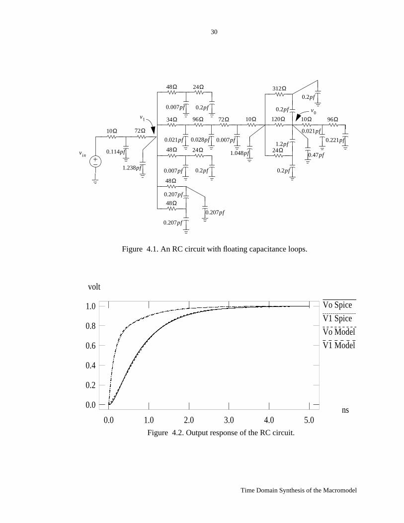
the delay modeling of VLSI interconnects. The first circuit, shown in Fig. 4.1, is an RC
network. Floating capacitors are present to form several loops. It took 0.2 CPU second to
analyze the circuit with one external output node and 0.3 CPU second for two external
output nodes, both using a second order macromodel. The output responses with a unit
step input, together with the results obtained by SPICE3e2 [39], are plotted in Fig. 4.2.
While there is little difference between the results based on macromodel and the SPICE
model, it took SPICE3e2 3.2 CPU second to compute the response. (CPU times are
measured on SUN-SPARC 1+).
We also compared our method with AWE-like simulator which is implemented in
30
Time Domain Synthesis of the Macromodel
Figure 4.1. An RC circuit with floating capacitance loops.
vin
1.238pf
0.114pf
10Ω
v1
72Ω
0.007pf
34Ω
48Ω
48Ω
48Ω
0.007pf
0.021pf
48Ω0.207pf
0.207pf
0.207pf
0.2pf
0.028pf
24Ω
72Ω96Ω
0.2pf
24Ω
0.007pf
1.048pf
10Ω
312Ω
0.2pf
120Ω
24Ω
0.2pf
1.2pf
v0
10Ω
0.47pf
0.021pf
0.2pf
0.221pf
96Ω
Figure 4.2. Output response of the RC circuit.
Vo Spice
V1 Spice
Vo Model
V1 Model
volt
ns0.0
0.2
0.4
0.6
0.8
1.0
0.0 1.0 2.0 3.0 4.0 5.0
31
Time Domain Synthesis of the Macromodel
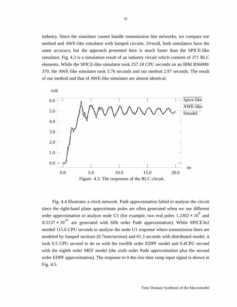
industry. Since the simulator cannot handle transmission line networks, we compare our
method and AWE-like simulator with lumped circuits. Overall, both simulators have the
same accuracy, but the approach presented here is much faster than the SPICE-like
simulator. Fig. 4.3 is a simulation result of an industry circuit which consists of 371 RLC
elements. While the SPICE-like simulator took 257.18 CPU seconds on an IBM RS6000/
370, the AWE-like simulator took 3.76 seconds and our method 2.97 seconds. The result
of our method and that of AWE-like simulator are almost identical.
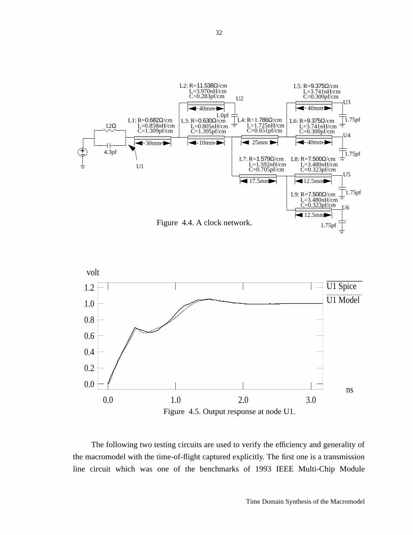
Fig. 4.4 illustrates a clock network. Padé approximation failed to analyze the circuit
since the right-hand plane approximate poles are often generated when we use different
order approximation to analyze node U1 (for example, two real poles and
are generated with fifth order Padé approximation). While SPICE3e2
needed 115.6 CPU seconds to analyze the node U1 response where transmission lines are
modeled by lumped sections (0.7mm/section) and 61.3 seconds with distributed model, it
took 0.5 CPU second to do so with the twelfth order EDPF model and 0.4CPU second
with the eighth order MEF model (the sixth order Padé approximation plus the second
order EDPF approximation). The response to 0.4ns rise time ramp input signal is shown in
Fig. 4.5.
Spice-like
AWE-like
Smodel
volt
ns0.0
1.0
2.0
3.0
4.0
5.0
6.0
0.0 5.0 10.0 15.0 20.0Figure 4.3. The responses of the RLC circuit.
1.2302 108×
8.5137 1010×
32
Time Domain Synthesis of the Macromodel
The following two testing circuits are used to verify the efficiency and generality of
the macromodel with the time-of-flight captured explicitly. The first one is a transmission
line circuit which was one of the benchmarks of 1993 IEEE Multi-Chip Module
30mm
17.5mm
25mm
12Ω
1.75pf
4.3pf
R=0.682Ω/cmL=0.858nH/cmC=1.309pf/cm
L1: R=1.786Ω/cmL=1.725nH/cmC=0.651pf/cm
L4:
R=1.579Ω/cmL=1.592nH/cmC=0.705pf/cm
L7:
10mm
R=0.630Ω/cmL=0.805nH/cmC=1.395pf/cm
L3:
40mm
R=11.538Ω/cmL=3.970nH/cmC=0.283pf/cm
L2:
40mm
40mm
R=7.500Ω/cmL=3.480nH/cmC=0.323pf/cm
L8:
1.0pf
1.75pf
1.75pf
1.75pf
U2U3
U4
U5
U6
U1
R=9.375Ω/cmL=3.741nH/cmC=0.300pf/cm
L5:
R=9.375Ω/cmL=3.741nH/cmC=0.300pf/cm
L6:
R=7.500Ω/cmL=3.480nH/cmC=0.323pf/cm
L9:
12.5mm
12.5mmFigure 4.4. A clock network.
Figure 4.5. Output response at node U1.
U1 Spice
U1 Model
volt
ns0.0
0.2
0.4
0.6
0.8
1.0
1.2
0.0 1.0 2.0 3.0
33
Time Domain Synthesis of the Macromodel
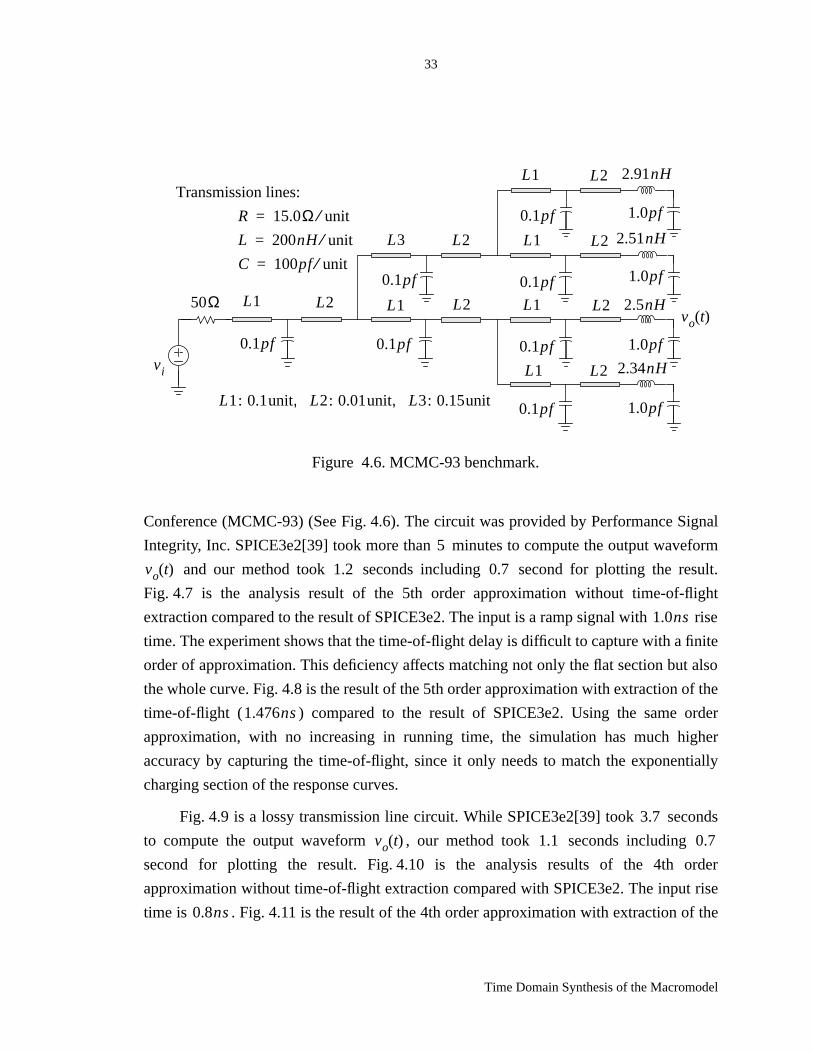
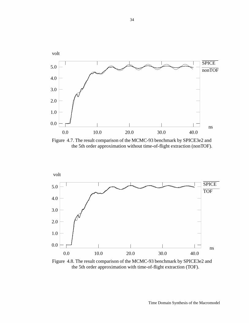
Conference (MCMC-93) (See Fig. 4.6). The circuit was provided by Performance Signal
Integrity, Inc. SPICE3e2[39] took more than minutes to compute the output waveform
and our method took seconds including second for plotting the result.
Fig. 4.7 is the analysis result of the 5th order approximation without time-of-flight
extraction compared to the result of SPICE3e2. The input is a ramp signal with rise
time. The experiment shows that the time-of-flight delay is difficult to capture with a finite
order of approximation. This deficiency affects matching not only the flat section but also
the whole curve. Fig. 4.8 is the result of the 5th order approximation with extraction of the
time-of-flight ( ) compared to the result of SPICE3e2. Using the same order
approximation, with no increasing in running time, the simulation has much higher
accuracy by capturing the time-of-flight, since it only needs to match the exponentially
charging section of the response curves.
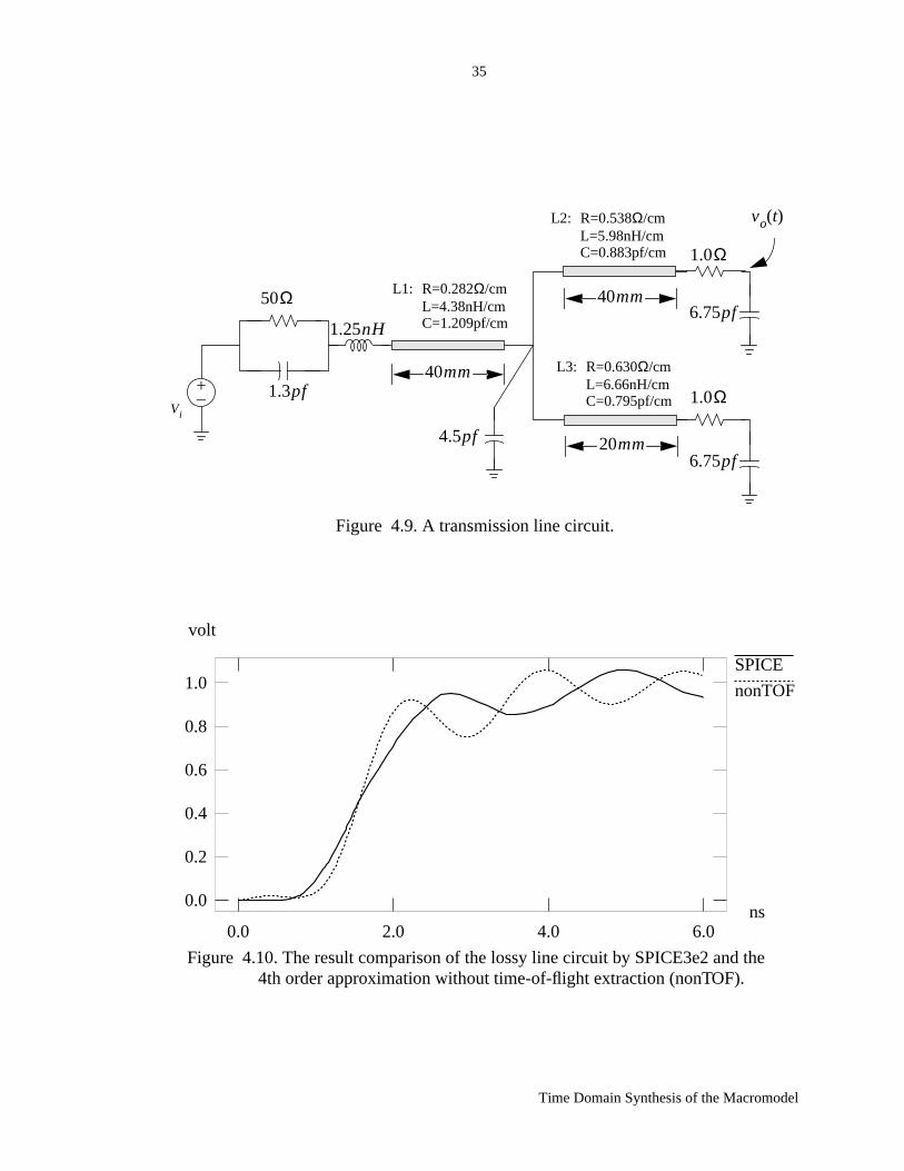
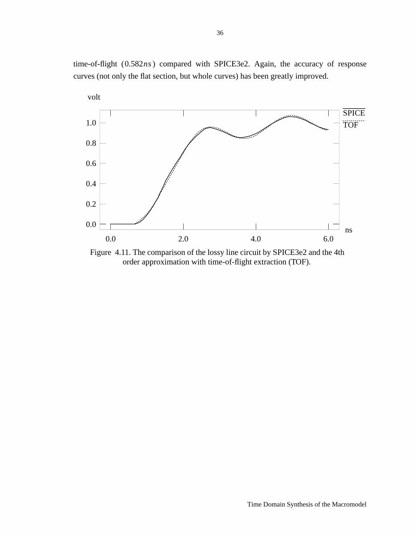
Fig. 4.9 is a lossy transmission line circuit. While SPICE3e2[39] took seconds
to compute the output waveform , our method took seconds including
second for plotting the result. Fig. 4.10 is the analysis results of the 4th order
approximation without time-of-flight extraction compared with SPICE3e2. The input rise
time is . Fig. 4.11 is the result of the 4th order approximation with extraction of the
Figure 4.6. MCMC-93 benchmark.
50Ω L1
2.91nH
0.1pf
1.0pf
vi
0.1pf
0.1pf
0.1pf
0.1pf
0.1pf
0.1pf
1.0pf
1.0pf
1.0pf
2.51nH
2.5nH
2.34nH
L1: 0.1unit, L2: 0.01unit L3: 0.15unit,
Transmission lines:
R 15.0Ω unit⁄=
L 200nH unit⁄=
C 100pf unit⁄=
L3
L1 L1
L1
L1
L1
L2
L2
L2
L2
L2
L2
L2
vo t( )
5
vo t( ) 1.2 0.7
1.0ns
1.476ns
3.7
vo t( ) 1.1 0.7
0.8ns
34
Time Domain Synthesis of the Macromodel
Figure 4.7. The result comparison of the MCMC-93 benchmark by SPICE3e2 andthe 5th order approximation without time-of-flight extraction (nonTOF).
SPICE
nonTOF
volt
ns0.0
1.0
2.0
3.0
4.0
5.0
0.0 10.0 20.0 30.0 40.0
Figure 4.8. The result comparison of the MCMC-93 benchmark by SPICE3e2 andthe 5th order approximation with time-of-flight extraction (TOF).
SPICE
TOF
volt
ns0.0
1.0
2.0
3.0
4.0
5.0
0.0 10.0 20.0 30.0 40.0
35
Time Domain Synthesis of the Macromodel
R=0.282Ω/cmL=4.38nH/cmC=1.209pf/cm
L1:
R=0.538Ω/cmL=5.98nH/cmC=0.883pf/cm
L2:
R=0.630Ω/cmL=6.66nH/cmC=0.795pf/cm
L3:
Vi
vo t( )
50Ω
+_ 1.3pf
1.25nH
40mm
4.5pf 20mm
40mm
1.0Ω
1.0Ω
6.75pf
6.75pf
Figure 4.9. A transmission line circuit.
Figure 4.10. The result comparison of the lossy line circuit by SPICE3e2 and the4th order approximation without time-of-flight extraction (nonTOF).
SPICE
nonTOF
volt
ns0.0
0.2
0.4
0.6
0.8
1.0
0.0 2.0 4.0 6.0
36
Time Domain Synthesis of the Macromodel
time-of-flight ( ) compared with SPICE3e2. Again, the accuracy of response
curves (not only the flat section, but whole curves) has been greatly improved.
0.582ns
Figure 4.11. The comparison of the lossy line circuit by SPICE3e2 and the 4thorder approximation with time-of-flight extraction (TOF).
SPICE
TOF
volt
ns0.0
0.2
0.4
0.6
0.8
1.0
0.0 2.0 4.0 6.0

37
Norton Equivalent Circuits Based on Recursive Convolution
CHAPTER 5 Norton Equivalent CircuitsBased on RecursiveConvolution
One of the fundamental difficulties encountered in integrating transmission line
simulation in a transient circuit simulator arises because the circuits containing nonlinear
devices must be characterized in the time domain while transmission lines with loss,
dispersion, and interconnect discontinuities are best modeled in the frequency domain. To
cope with this difficulty, direct convolution techniques are used. The system outputs are
the convolutions of the inputs with the impulse responses. The fundamental problem lies
in how to determine the impulse response of an arbitrary interconnect system. Another
drawback of the direct convolution is time consuming. While explicit analytical
expression of the impulse responses is impractical, the numerical inverse Fast Fourier
Transformation technique suffers from the fact that an excessive number of frequency
points are needed to avoid aliasing effects [54].
We have presented a scattering-parameter-based macromodel to analyze
interconnect systems. The Exponentially-Decayed Polynomial Function (EDPF) or
Mixed-Exponential Function (MEF) are used to get an approximated explicit analytical
expression of the transfer function. MEF is the combination of exponential functions and
EDPF. Reference [73] gives the derivation of the recursive convolution formula of an
exponential with any input function. Actually, an exponential is a special function of the
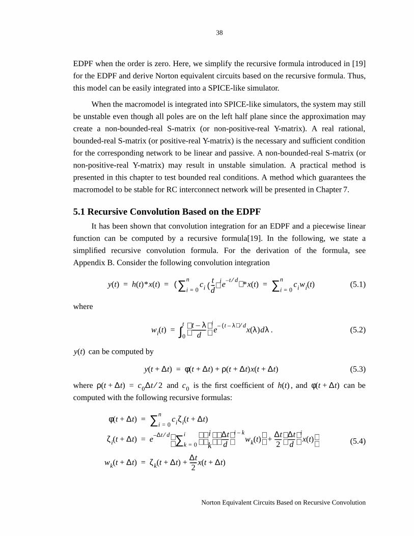
38
Norton Equivalent Circuits Based on Recursive Convolution
EDPF when the order is zero. Here, we simplify the recursive formula introduced in [19]
for the EDPF and derive Norton equivalent circuits based on the recursive formula. Thus,
this model can be easily integrated into a SPICE-like simulator.
When the macromodel is integrated into SPICE-like simulators, the system may still
be unstable even though all poles are on the left half plane since the approximation may
create a non-bounded-real S-matrix (or non-positive-real Y-matrix). A real rational,
bounded-real S-matrix (or positive-real Y-matrix) is the necessary and sufficient condition
for the corresponding network to be linear and passive. A non-bounded-real S-matrix (or
non-positive-real Y-matrix) may result in unstable simulation. A practical method is
presented in this chapter to test bounded real conditions. A method which guarantees the
macromodel to be stable for RC interconnect network will be presented in Chapter 7.
5.1 Recursive Convolution Based on the EDPF
It has been shown that convolution integration for an EDPF and a piecewise linear
function can be computed by a recursive formula[19]. In the following, we state a
simplified recursive convolution formula. For the derivation of the formula, see
Appendix B. Consider the following convolution integration
(5.1)
where
. (5.2)
can be computed by
(5.3)
where and is the first coefficient of , and can be
computed with the following recursive formulas:
(5.4)
y t( ) h t( )* x t( ) citd---( )
iet d⁄–
i 0=
n∑( ) * x t( ) ciwi t( )i 0=
n∑= = =
wi t( )t λ–
d----------
ie
t λ–( ) d⁄–x λ( )dλ
0
t
∫=
y t( )
y t ∆t+( ) φ t ∆t+( ) ρ t ∆t+( )x t ∆t+( )+=
ρ t ∆t+( ) c0∆t 2⁄= c0 h t( ) φ t ∆t+( )
φ t ∆t+( ) ciζi t ∆t+( )i 0=
n∑=
ζi t ∆t+( ) e∆t d⁄– i
k ∆t
d-----
i k–wk t( )
k 0=
i∑ ∆t2----- ∆t
d-----
ix t( )+
=
wk t ∆t+( ) ζk t ∆t+( )∆t2-----x t ∆t+( )+=

39
Norton Equivalent Circuits Based on Recursive Convolution
5.2 Norton Equivalent Circuits
In order to incorporate the macromodel described with S-matrix, shown in
Fig. 2.2, into SPICE like simulators, we derive a Norton equivalent circuit. By modifying
the approach in [81], we insert two series impedances and at each port to remove
the effect of the reference impedance. Thus a virtual node is created between the load and
the macromodel as shown in Fig. 5.1 where is the node voltage in frequency domain at
port and is referred to as the virtual voltage at port . These variables are related by
(5.5)
where is the current flowing into the macromodel at port . From the definition of S-
parameters and the relation between circuit parameters and wave parameters, we have
(5.6)
(5.7)
where is an element of the S-matrix of the multiport component, and and are the
incoming wave and outgoing wave at port , respectively. From Eqs. (5.5) and (5.7), we
get
(5.8)
n n×
Z0 Z0–
2
V1
1
n
Sn n×
V'1 V1
Vn V'nVn
V2 V'2 V2Z0
Z0 Z– 0
Z– 0 Z0
Source or arbitrary termination
Z– 0
Figure 5.1. Macromodel with virtual nodes.
Vi
i V'i i
V'i Vi Z0I i+= i 1 … N, ,=
I i i
bi Sij ajj 1=
N∑=
Vi ai bi+= , Z0Ii
ai bi–=
Sij ai bi
i
ai V'i 2⁄=
40
Norton Equivalent Circuits Based on Recursive Convolution
Rewriting Eq. (5.5) and combining it with Eqs. (5.6), (5.7) and (5.8), the
macromodel system can be described by the following equation:
(5.9)
Writing this equation in the time domain leads to the convolution equation
(5.10)
Since S-parameters are modeled with EDPF, using the recursive convolution
formula Eqs. (5.3) and (5.4), Eq. (5.10) can be written with
(5.11)
where
(5.12)
(5.13)
A Norton equivalent circuit can be derived from Eq. (5.11) and it can be easily
integrated into SPICE-like simulators. The equivalent circuit of a two port macromodel is
shown in Fig. 5.2.
5.3 Stability of Macromodel
As pointed out in [16, 1, 22], the Padé approximation suffers from the instability
I i Z01–V'i Z0
1–Vi–=
Z01–V'i Z0
1–ai bi+( )–=
Z01–V'i Z0
1–ai Sij ajj 1=
N∑+( )–=
12---Z
0
1–V'i
12---Z
0
1–Sij V'jj 1=
N∑–=
i i t( )Z0
1–
2--------v'i t( )
Z01–
2-------- Sij * v'j t( )
j 1=
N∑–=
i i t( )Z0
1–
2--------v'i t( )
Z01–
2-------- φj t( ) ρj t( ) v'j t( )+( )
j 1=
N∑–=
gij t( ) v'i t( )j 1=
N∑ Isi t( )–=
Isi t( )Z0
1–
2-------- φj t( )
j 1=
N∑=
gij t( )Z0
1–1 ρj t( )–( ) 2⁄ i j=
Z01– ρj t( )– 2⁄ i j≠
=
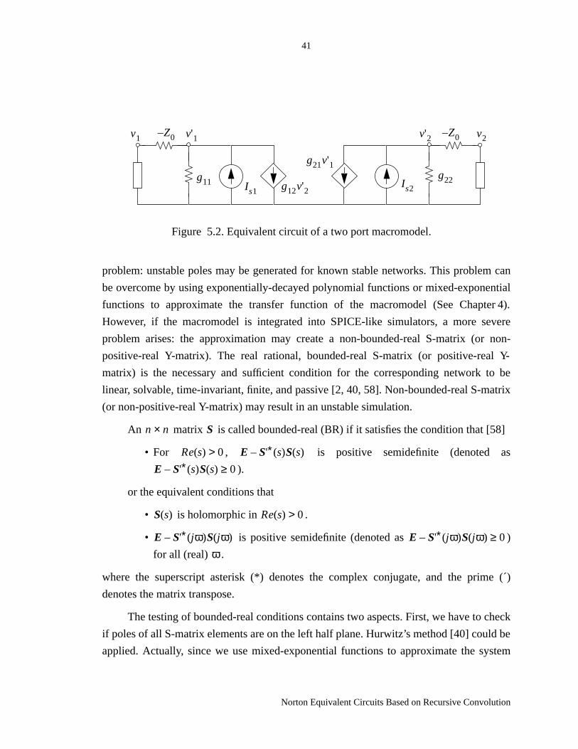
41
Norton Equivalent Circuits Based on Recursive Convolution
problem: unstable poles may be generated for known stable networks. This problem can
be overcome by using exponentially-decayed polynomial functions or mixed-exponential
functions to approximate the transfer function of the macromodel (See Chapter 4).
However, if the macromodel is integrated into SPICE-like simulators, a more severe
problem arises: the approximation may create a non-bounded-real S-matrix (or non-
positive-real Y-matrix). The real rational, bounded-real S-matrix (or positive-real Y-
matrix) is the necessary and sufficient condition for the corresponding network to be
linear, solvable, time-invariant, finite, and passive [2, 40, 58]. Non-bounded-real S-matrix
(or non-positive-real Y-matrix) may result in an unstable simulation.
An matrix is called bounded-real (BR) if it satisfies the condition that [58]
• For , is positive semidefinite (denoted as
).
or the equivalent conditions that
• is holomorphic in .
• is positive semidefinite (denoted as )
for all (real) .
where the superscript asterisk (*) denotes the complex conjugate, and the prime (´)
denotes the matrix transpose.
The testing of bounded-real conditions contains two aspects. First, we have to check
if poles of all S-matrix elements are on the left half plane. Hurwitz’s method [40] could be
applied. Actually, since we use mixed-exponential functions to approximate the system
v1 v'1
Is1
Z– 0
g11 g12v'2
v2v'2
Is2
Z– 0
g22
g21v'1
Figure 5.2. Equivalent circuit of a two port macromodel.
n n× S
Re s( ) 0> E S'∗ s( )S s( )–
E S'∗ s( )S s( )– 0≥
S s( ) Re s( ) 0>
E S'∗ jω( )S jω( )– E S'∗ jω( )S jω( )– 0≥ω
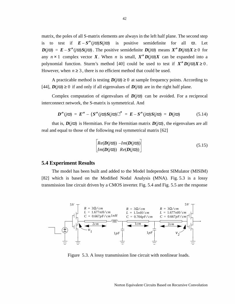
42
Norton Equivalent Circuits Based on Recursive Convolution
matrix, the poles of all S-matrix elements are always in the left half plane. The second step
is to test if is positive semidefinite for all . Let
. The positive semidefinite means for
any complex vector . When is small, can be expanded into a
polynomial function. Sturm’s method [40] could be used to test if .
However, when , there is no efficient method that could be used.
A practicable method is testing at sample frequency points. According to
[44], if and only if all eigenvalues of are in the right half plane.
Complex computation of eigenvalues of can be avoided. For a reciprocal
interconnect network, the S-matrix is symmetrical. And
(5.14)
that is, is Hermitian. For the Hermitian matrix , the eigenvalues are all
real and equal to those of the following real symmetrical matrix [62]
(5.15)
5.4 Experiment Results
The model has been built and added to the Model Independent SIMulator (MISIM)
[82] which is based on the Modified Nodal Analysis (MNA). Fig. 5.3 is a lossy
transmission line circuit driven by a CMOS inverter. Fig. 5.4 and Fig. 5.5 are the response
E S'∗ jω( )S jω( )– ωD jω( ) E S'∗ jω( )S jω( )–= D jω( ) X'∗D jω( )X 0≥
n 1× X n X'∗D jω( )X
X'∗D jω( )X 0≥n 3≥
D jω( ) 0≥D jω( ) 0≥ D jω( )
D jω( )
D'∗ jω( ) E'∗ S'∗ jω( )S jω( )( ) '∗– E S'∗ jω( )S jω( )– D jω( )= = =
D jω( ) D jω( )
ReD jω( )( ) Im D jω( )( )–
Im D jω( )( ) ReD jω( )( )
5V 5V
v1 v2
R 3Ω cm⁄=L 1.677nH cm⁄=C 0.667pF cm⁄=
2cm
1nH
1pF
R 3Ω cm⁄=L 1.5nH cm⁄=C 0.704pF cm⁄=
R 3Ω cm⁄=L 1.677nH cm⁄=C 0.667pF cm⁄=
1pF
1cm 2cm
Figure 5.3. A lossy transmission line circuit with nonlinear loads.
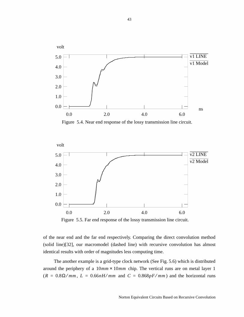
43
Norton Equivalent Circuits Based on Recursive Convolution
of the near end and the far end respectively. Comparing the direct convolution method
(solid line)[32], our macromodel (dashed line) with recursive convolution has almost
identical results with order of magnitudes less computing time.
The another example is a grid-type clock network (See Fig. 5.6) which is distributed
around the periphery of a chip. The vertical runs are on metal layer 1
( , and ) and the horizontal runs
Figure 5.4. Near end response of the lossy transmission line circuit.
v1 LINE
v1 Model
volt
ns0.0
1.0
2.0
3.0
4.0
5.0
0.0 2.0 4.0 6.0
Figure 5.5. Far end response of the lossy transmission line circuit.
v2 LINE
v2 Model
volt
0.0
1.0
2.0
3.0
4.0
5.0
0.0 2.0 4.0 6.0
10mm 10mm×R 0.8Ω mm⁄= L 0.66nH mm⁄= C 0.868pF mm⁄=

44
Norton Equivalent Circuits Based on Recursive Convolution
are on metal layer 2 ( , and ).
The network is represented by distributed lossy transmission lines driven by a CMOS
inverter. Fig. 5.7 is the curve of the driver output and Fig. 5.8 is the curves of . There
is little difference between the results based on our macromodel and the SPICE model.
While it took more than 500 CPU seconds on SUN SPARC 1+ for SPICE3e2 to get the
answer using the direct convolution [70], our program took 56.3 seconds to analyze the
circuit using 12th order MEF approximation.
We also integrated the macromodel into Intel internal simulator TIM. The same
circuit topology of Figure 5.6 is also tested in TIM with different order of approximation.
The vertical runs are on metal layer 1 ( , and
) and the horizontal runs are on metal layer 2 ( ,
and ). The ratios of channel width and length of
the driver are for pMOS and for nMOS. The ratios of channel width and length
of the receiver are for pMOS and for nMOS. The output responses of (See
Figure 5.6) with different order approximation are shown in Figure 5.9.
Several more circuits driven by nonlinear drivers are tested in TIM. The results are
5V
5V
v1
10mm
1.75pF 1.75pF
10m
m
1.75pF 1.75pF
1.75pF1.75pF
vo
Figure 5.6. Grid-type clock network.
v2
R 1.0Ω mm⁄= L 0.826nH mm⁄= C 0.694pF mm⁄=
v1 vo
R 1.6Ω mm⁄= L 0.66nH mm⁄=
C 0.868pF mm⁄= R 2.0Ω mm⁄=
L 0.826nH mm⁄= C 0.694pF mm⁄=
400 200
40 20 v2
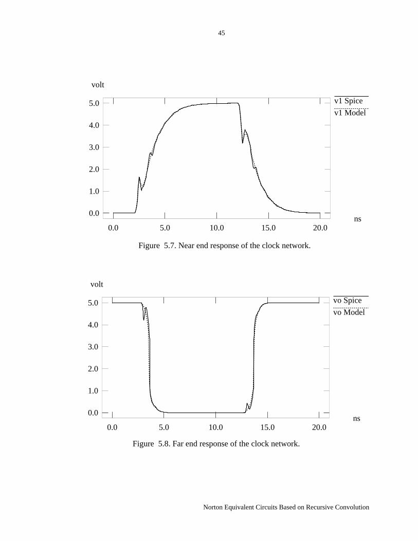
45
Norton Equivalent Circuits Based on Recursive Convolution
Figure 5.7. Near end response of the clock network.
v1 Spice
v1 Model
volt
ns0.0
1.0
2.0
3.0
4.0
5.0
0.0 5.0 10.0 15.0 20.0
Figure 5.8. Far end response of the clock network.
vo Spice
vo Model
volt
ns0.0
1.0
2.0
3.0
4.0
5.0
0.0 5.0 10.0 15.0 20.0

46
Norton Equivalent Circuits Based on Recursive Convolution
shown in Table 5.1. Note that the time for macromodel to do DC analysis includes the
time of model reduction. From the table, we can see that the efficiency is more evident for
the larger circuits.
*. The number includes the time for model reduction.
circuits# of
elements
time for DC analysis time for transient analysis
TIM S-model* TIM S-model
Circuit 1 82 0.01 0.18 0.26 0.06
Circuit 2 180 0.47 0.46 2.44 0.80
Circuit 3 373 0.03 0.78 23.64 0.78
Circuit 4 11216 28.09 1.07 135.72 19.82
Table 5.1: Comparison of the macromodel and TIM.
Figure 5.9. Comparison of different order approximation.
TIM
7th order
9th order
10th order
12th order
volt
ns0.0
1.0
2.0
3.0
4.0
5.0
0.0 5.0 10.0 15.0 20.0

47
Partitioning of Interconnect Networks
CHAPTER 6 Partitioning of InterconnectNetworks
When fast timing analysis is desired for today’s complex interconnect structures,
moment matching techniques are widely used to approximate a higher order linear
network using the waveforms generated by its lower order moments [49, 54, 60]. These
approaches can also be used to improve the efficiency of existing time-domain circuit
simulators by incorporating macromodels of the interconnect networks together with
recursive convolution [49, 54, 64], or generating an equivalent circuit based on a
numerical integration method [40].
The macromodels generated by moment matching technique are approximations of
the port behavior of the interconnects. In order to incorporate the macromodels into
SPICE-like simulators, they are usually described by an admittance matrix (Y-matrix) [64,
40]. The Y-matrices are generally full matrices. When the number of external ports of an
interconnect network is large, the number of entries of the matrix may be larger than the
number of circuit elements of the original interconnect network. For example, a clock
network with 500 fanouts will create more than 250,000 entries of the corresponding Y-
matrix. This huge full matrix may even increase the computational burden of traditional
SPICE simulation.
On the other hand, trying to model the huge full matrix by lower order
approximation with moment matching techniques is impractical. Severe numerical
problems may result in extremely ill-conditioned matrices for computing high order
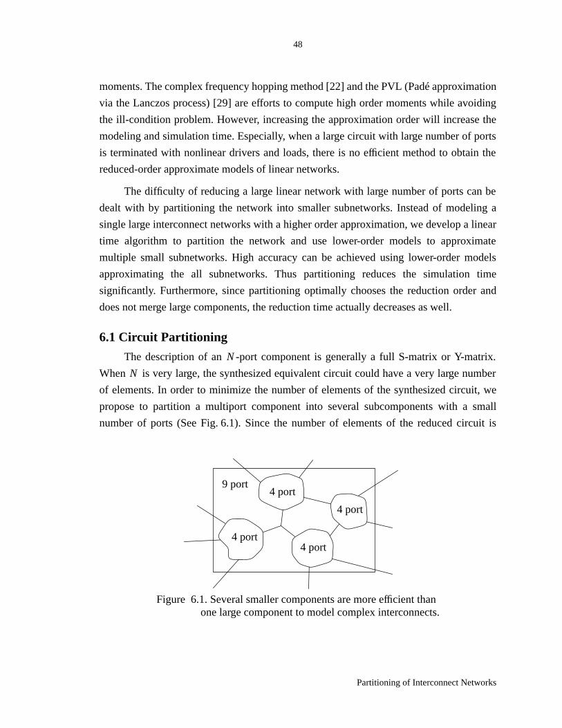
48
Partitioning of Interconnect Networks
moments. The complex frequency hopping method [22] and the PVL (Padé approximation
via the Lanczos process) [29] are efforts to compute high order moments while avoiding
the ill-condition problem. However, increasing the approximation order will increase the
modeling and simulation time. Especially, when a large circuit with large number of ports
is terminated with nonlinear drivers and loads, there is no efficient method to obtain the
reduced-order approximate models of linear networks.
The difficulty of reducing a large linear network with large number of ports can be
dealt with by partitioning the network into smaller subnetworks. Instead of modeling a
single large interconnect networks with a higher order approximation, we develop a linear
time algorithm to partition the network and use lower-order models to approximate
multiple small subnetworks. High accuracy can be achieved using lower-order models
approximating the all subnetworks. Thus partitioning reduces the simulation time
significantly. Furthermore, since partitioning optimally chooses the reduction order and
does not merge large components, the reduction time actually decreases as well.
6.1 Circuit Partitioning
The description of an -port component is generally a full S-matrix or Y-matrix.
When is very large, the synthesized equivalent circuit could have a very large number
of elements. In order to minimize the number of elements of the synthesized circuit, we
propose to partition a multiport component into several subcomponents with a small
number of ports (See Fig. 6.1). Since the number of elements of the reduced circuit is
N
N
4 port
4 port
4 port4 port
9 port
Figure 6.1. Several smaller components are more efficient thanone large component to model complex interconnects.

49
Partitioning of Interconnect Networks
proportional to the number of the entries of S-matrix, the objective of the partitioning
problem is to minimize the total number of entries of the S-matrix. More precisely,
(6.1)
where is the number of subcomponents and the number of ports of the component .
We propose a linear-time heuristic algorithm to partition the interconnect network into
several multiport components.
Consider the circuit graph of a network , where vertices consists of circuit
elements shown in Fig. 2.1 and edges represent the adjacency between elements in the
circuit. Define the weight of an edge as the number of ports of the resultant
component after contracting with Adjoined Merging (Fig. 2.3) or Self Merging
(Fig. 2.4). We bound the weight of “contractible” edges by . When an edge has the
weight more than , it will not be contracted during network reduction, and when
weights of all edges are greater than , the reduction process terminates. Here
is chosen in such a way that the number of matrix entries does not increase too much when
contracting the edges. Let and be the port numbers of the two different
components connected by an edge . According to the definition, .
is chosen such that for any , the following inequality holds,
(6.2)
where is the number of entries of S-matrices before contracting ,
is that after contracting , and the contracting factor. Based on
experience, the typical is between 0.75 and 1.0, or the corresponding is between
five and eight. The following is the pseudo code of the network reduction algorithm:
Algorithm Network-Reduction
Compute weights of all edges
← the edge with minimal weight
while ( )
Contract
Update weights of all edges incident to
← the edge with minimal weight
minimize Ni2
i 1=
χ∑χ Ni i
G V E,( ) V
E
W e( ) e E∈e
Wmax
Wmax
Wmax Wmax
Nx Ny
e W e( ) Nx Ny 2–+=
Wmax e
Nx2
Ny2
+ β Nx Ny 2–+( ) 2>
Nx2
Ny2
+ e
Nx Ny 2–+( ) 2e β
β Wmax
emin
W emin( ) Wmax<
emin
emin
emin

50
Partitioning of Interconnect Networks
end-while
Now we have two problems: one is how to select efficiently an edge with minimum
weight, and the other is how to update the edge weights after contracting an edge. Those
operations can be done in constant time with a bucket list structure shown in Fig. 6.2. This
structure includes a bucket array, whose th entry contains a doubly-linked list of edges
with weights equal to . For the bucket array, a index is used to keep track of
the bucket containing edges with the minimum weight. Since only neighboring edges
change their weights, these weights can be updated in constant time [31].
6.2 Efficiency and Accuracy of Reduced Networks
The common method to increase accuracy of modeling a large interconnect network
with moment matching techniques is to increase approximation order [22, 29, 41]. This
will increase the modeling and simulation time. The problem becomes evident when the
number of port is very large. As stated in [41],
“The generation of the y-parameters for a specified multiport network is achieved by
exciting the network with an impulse voltage at one of the ports while shorting all other
ports. Measuring the currents at each of the ports then yields one column of the Y-matrix.
This procedure is repeated at each of the network ports to obtain the complete
description”.
Only recently, an improved PVL method [30] were proposed to compute the
reduced-order approximate models of linear networks with multiple inputs and outputs.
Wmax
edge#
1
edge#minweight
Figure 6.2. Bucket list structure.
i
i minweight

51
Partitioning of Interconnect Networks
However, the huge full Y-matrix with high order of approximation will still be a heavy
burden on simulation.
Instead of modeling a single large interconnect networks with higher order
approximation, we partition the network and use lower-order models to approximate
multiple small subnetworks. High accuracy can be achieved using lower-order models
approximating the all subnetworks. The accuracy can be controlled by adjusting the
number of subnetworks, or equivalently by adjusting the number of original circuit
elements in each subnetwork. The partitioning reduces the simulation time significantly.
Furthermore, since partitioning optimally chooses the reduction order and does not merge
large components, the reduction time actually decreases.
In addition, partitioning greatly reduces the number of elements in the reduced
circuits. When using a Y-matrix to describe the port behavior of a network, the number of
y-elements is , where is the number of external ports. However, as we will show
in experimental results in the Chapter 7, for typical clock networks, the number of circuit
elements in reduced circuits with partitioning is .
O N2
( ) N
O N( )
52
Circuit Synthesis of RC Networks
CHAPTER 7 Circuit Synthesis of RCNetworks
To extract accurately the interconnect networks on chips, the number of parasitic
resistors and capacitors can overwhelm any circuit simulator. A new transient analysis
strategy for complex RC interconnect networks is proposed in this Chapter. With the
circuit partitioning we proposed in Chapter 6, a large RC interconnect network is reduced
into subnetworks which are approximated with lower-order equivalent RC circuits. The
number of RC elements can be reduced between 50% and 90% (80% is typical). The
reduced circuits are guaranteed to be stable. The reduced-order approximate models of
linear networks with multiple inputs and outputs can be obtained in one pass of reduction.
The reduced circuits can be simulated using existing circuit simulators without
modification. The experiment results show that the number of circuit elements in a
reduced network is for typical clock networks, where is the number of external
ports. The simulation time can be reduced by two to three orders of magnitude while error
is less than 5% compared to the original circuits.
7.1 Circuit Synthesis of RC Interconnect Networks
Given the scattering matrix of a multiport component, the admittance matrix is
(7.1)
where is the reference impedance, and identity matrix. The synthesis of a general Y-
O N( ) N
S
Y Z01–
E S+( ) 1–E S–( )=
Z0 E
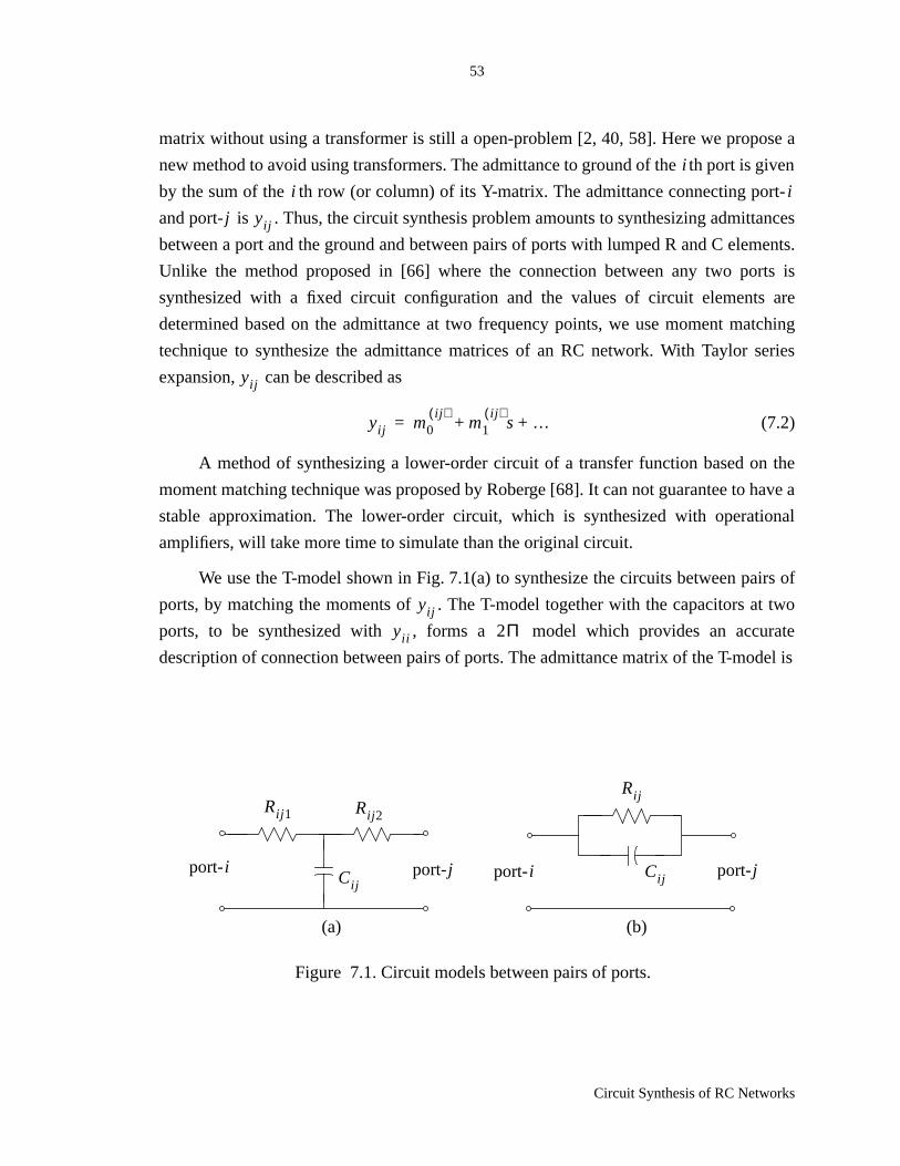
53
Circuit Synthesis of RC Networks
matrix without using a transformer is still a open-problem [2, 40, 58]. Here we propose a
new method to avoid using transformers. The admittance to ground of the th port is given
by the sum of the th row (or column) of its Y-matrix. The admittance connecting port-
and port- is . Thus, the circuit synthesis problem amounts to synthesizing admittances
between a port and the ground and between pairs of ports with lumped R and C elements.
Unlike the method proposed in [66] where the connection between any two ports is
synthesized with a fixed circuit configuration and the values of circuit elements are
determined based on the admittance at two frequency points, we use moment matching
technique to synthesize the admittance matrices of an RC network. With Taylor series
expansion, can be described as
(7.2)
A method of synthesizing a lower-order circuit of a transfer function based on the
moment matching technique was proposed by Roberge [68]. It can not guarantee to have a
stable approximation. The lower-order circuit, which is synthesized with operational
amplifiers, will take more time to simulate than the original circuit.
We use the T-model shown in Fig. 7.1(a) to synthesize the circuits between pairs of
ports, by matching the moments of . The T-model together with the capacitors at two
ports, to be synthesized with , forms a model which provides an accurate
description of connection between pairs of ports. The admittance matrix of the T-model is
i
i i
j yij
yij
yij m0ij( )
m1ij( )
s …+ +=
Figure 7.1. Circuit models between pairs of ports.
Rij 1 Rij 2
Cijport-i port-j
Rij
Cijport-i port-j
(a) (b)
yij
yii 2Π
54
Circuit Synthesis of RC Networks
(7.3)
By expanding Eq. (7.3) into Taylor series, we have
(7.4)
In order to determine the values of , and , let
(7.5)
The reason why we match , and not match and directly, is
that and are the second moments of and which are total contribution of
the circuit, not just a branch between port- and port- . Solving Eqs. (7.3), (7.4) and (7.5),
we have
(7.6)
yii1
Rij 1---------
Rij 2
Rij 1 Rij 1 Rij 2 sCij Rij 1Rij 2+ +( )----------------------------------------------------------------------------–=
yjj1
Rij 2---------
Rij 1
Rij 2 Rij 1 Rij 2 sCij Rij 1Rij 2+ +( )----------------------------------------------------------------------------–=
yij yji1–
Rij 1 Rij 2 sCij Rij 1Rij 2+ +-----------------------------------------------------------= =
m0ii( )
m0jj( )
m0ij( )
– 1Rij 1 Rij 2+------------------------= = =
m1ii( ) Cij Rij 2
2
Rij 1 Rij 2+( ) 2----------------------------------= m1
jj( ) Cij Rij 12
Rij 1 Rij 2+( ) 2----------------------------------=
m1ij( ) Cij Rij 1Rij 2
Rij 1 Rij 2+( ) 2----------------------------------=
Rij 1 Rij 2 Cij
m0ij( )
m0ij( )
= m1ij( )
m1ij( )
=m1
ii( )
m1jj( )------------
m1ii( )
m1jj( )------------=
m1ii( )
m1jj( )⁄ m1
ii( )m1
jj( )
m1ii( )
m1jj( )
yii yjj
i j
Rij 1
m1jj( )
–
m0ij( )
m1ii( )
m1jj( )
+( )-----------------------------------------------------------=
Rij 2
m1ii( )
–
m0ij( )
m1ii( )
m1jj( )
+( )-----------------------------------------------------------=
Cij
m1ii( )
m1jj( )
+( ) 2m1
ij( )
m1ii( )
m1jj( )
-------------------------------------------------------------=

55
Circuit Synthesis of RC Networks
The above formulas could be used to synthesize all off-diagonal elements of Y-
matrix with . However, if there are floating capacitors, may be negative. In
this case, we can also use a floating capacitor to model the between port- and port-
(see Fig. 7.1(b)). The admittance matrix of the model is
(7.7)
Thus, we have
(7.8)
For the diagonal elements , we need to synthesize , where
(7.9)
The is modelled with a parallel RC elements of Fig. 7.2. If there is no DC path
from port- to ground, . The is modelled with a single capacitor. In general,
the parameters of the model are
(7.10)
In case the capacitor computed in Eq. (7.10) is negative, we can set and
scale up all to keep total capacitance unchanged. Let be the new capacitance
m1ij( )
0≥ m1ij( )
yij i j
yii yjj yij–= =
1Rij------ sCij+=
Rij1–
m0ij( )------------= Cij m1
ij( )–=
yii yi0
yi0 yii yii∑–=
m0i0( )
m1i0( )
s …+ +=
yi0
i mi00 0= yi0
Rii1
m0i0( )-------------= Cii m1
i0( )=
Figure 7.2. RC parallel model of a port.
Riiport-i Cii
Cii Cii 0=
Cij C'ij
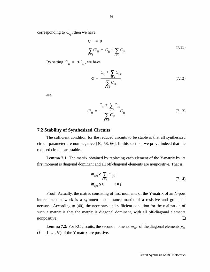
56
Circuit Synthesis of RC Networks
corresponding to , then we have
(7.11)
By setting , we have
(7.12)
and
(7.13)
7.2 Stability of Synthesized Circuits
The sufficient condition for the reduced circuits to be stable is that all synthesized
circuit parameter are non-negative [40, 58, 66]. In this section, we prove indeed that the
reduced circuits are stable.
Lemma 7.1:The matrix obtained by replacing each element of the Y-matrix by its
first moment is diagonal dominant and all off-diagonal elements are nonpositive. That is,
(7.14)
Proof: Actually, the matrix consisting of first moments of the Y-matrix of an N-port
interconnect network is a symmetric admittance matrix of a resistive and grounded
network. According to [40], the necessary and sufficient condition for the realization of
such a matrix is that the matrix is diagonal dominant, with all off-diagonal elements
nonpositive.
Lemma 7.2:For RC circuits, the second moments of the diagonal elements
( ) of the Y-matrix are positive.
Cij
C'ii 0=
C'iji j≠∑ Cii Cij
i j≠∑+=
C'ij αCij=
αCii Cik
i k≠∑+
Ciki k≠∑
-----------------------------=
C'ij
Cii Ciki k≠∑+
Ciki k≠∑
-----------------------------Cij=
mii 0 mij 0i j≠∑≥
mij 0 0≤ i j≠
mii 1 yii
i 1 … N, ,=
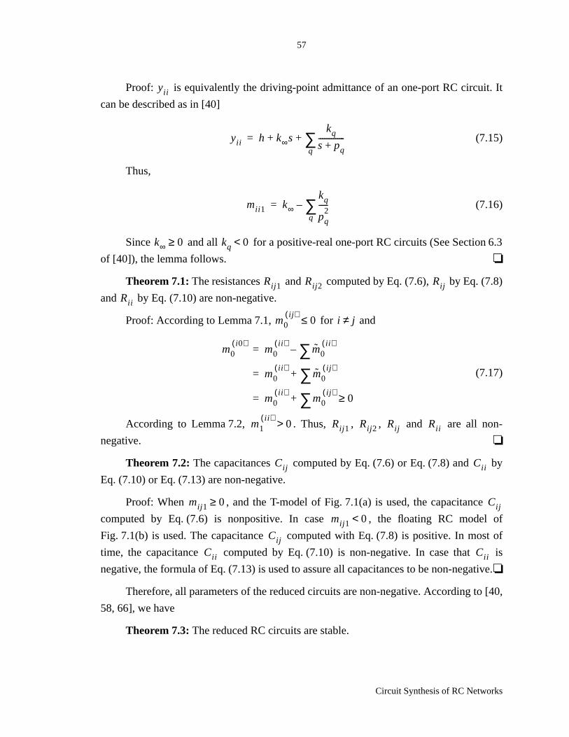
57
Circuit Synthesis of RC Networks
Proof: is equivalently the driving-point admittance of an one-port RC circuit. It
can be described as in [40]
(7.15)
Thus,
(7.16)
Since and all for a positive-real one-port RC circuits (See Section 6.3
of [40]), the lemma follows.
Theorem 7.1:The resistances and computed by Eq. (7.6), by Eq. (7.8)
and by Eq. (7.10) are non-negative.
Proof: According to Lemma 7.1, for and
(7.17)
According to Lemma 7.2, . Thus, , , and are all non-
negative.
Theorem 7.2:The capacitances computed by Eq. (7.6) or Eq. (7.8) and by
Eq. (7.10) or Eq. (7.13) are non-negative.
Proof: When , and the T-model of Fig. 7.1(a) is used, the capacitance
computed by Eq. (7.6) is nonpositive. In case , the floating RC model of
Fig. 7.1(b) is used. The capacitance computed with Eq. (7.8) is positive. In most of
time, the capacitance computed by Eq. (7.10) is non-negative. In case that is
negative, the formula of Eq. (7.13) is used to assure all capacitances to be non-negative.
Therefore, all parameters of the reduced circuits are non-negative. According to [40,
58, 66], we have
Theorem 7.3:The reduced RC circuits are stable.
yii
yii h k∞skq
s pq+--------------
q∑+ +=
mii 1 k∞kq
pq2
-----q∑–=
k∞ 0≥ kq 0<
Rij 1 Rij 2 Rij
Rii
m0ij( )
0≤ i j≠
m0i0( )
m0ii( )
m0ii( )∑–=
m0ii( )
m0ij( )∑+=
m0ii( )
m0ij( )∑+ 0≥=
m1ii( )
0> Rij 1 Rij 2 Rij Rii
Cij Cii
mij 1 0≥ Cij
mij 1 0<Cij
Cii Cii

58
Circuit Synthesis of RC Networks
7.3 Experimental Results
To illustrate the efficiency and generality of the proposed approach, some industry
circuits were tested. We compare results of the original circuits and the reduced circuits
using SPICE3e2 [39] on a Sun Sparc 20 workstation.
The first circuit is a clock network which consists of 26747 RC elements and has 547
external ports. The number of RC elements is reduced to 2084 which is less than 10% of
that of the original circuit. Consequently, the simulation time (SPICE3e2) is reduced from
202.8 seconds to 4.4 seconds. The number of elements and simulation time could be
further reduced if fewer external ports were of interest. For example, only ports on critical
paths may be of interest. Table 7.1 shows the reduction results for different number of
external ports. The number of circuit elements in reduced circuits versus the number of
external ports is plotted in Fig. 7.3. The figure shows that the number of reduced circuit
elements is , where is the number of external ports. The simulation time versus
the number of external ports is plotted in Fig. 7.4. Simulation results at the same port of
those reduced circuits with different number of ports are almost identical (See Fig. 7.5).
The error of the simulation results is less than 2%.
The reduction results of a loop-circuit and a mesh-circuit are shown in Table 7.2.
# of ports# of
elementsreductiontime (sec.)
simulationtime (sec.)
2 11 39.1 0.2
6 24 38.0 0.3
12 43 40.6 0.3
22 84 38.2 0.3
52 198 36.8 0.5
102 387 38.6 0.8
202 765 44.0 1.5
302 1154 42.9 2.4
402 1537 45.3 3.3
502 1906 57.3 3.9
547 2084 55.7 4.4
Original 26747 — 202.8
Table 7.1: The clock network reduction for different number of ports
O N( ) N
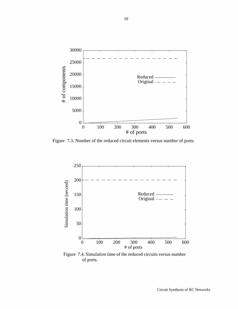
59
Circuit Synthesis of RC Networks
Figure 7.3. Number of the reduced circuit elements versus number of ports.
0
5000
10000
15000
20000
25000
30000
0 100 200 300 400 500 600
ReducedOriginal
# of
com
pone
nts
# of ports
Figure 7.4. Simulation time of the reduced circuits versus numberof ports.
0
50
100
150
200
250
0 100 200 300 400 500 600
ReducedOriginal
# of ports
Sim
ulat
ion
time
(sec
ond)
60
Circuit Synthesis of RC Networks
After reduction, the simulation time of the loop-circuit and the mesh-circuit was reduced
7.7 times and 20 times, respectively. The error of the simulation results is less than 2%,
compared with the original circuits.
The circuit partitioning plays a very important role in the circuit reduction. Another
clock circuit consists of 14034 RC elements with 1953 external ports (7.19 elements per
port). If we use only a simple multiport macromodel, the number of elements in the
synthesized circuit would be much more than that of the original circuit. However, since
the efficient combination of partitioning and reduction, the reduced circuit which keeps all
1953 ports external has only 8186 RC elements (4.19 elements per port).
The circuit reduction provides a new strategy to handle nonlinear circuits. A seven-
port clock network with nonlinear drivers and loads is shown in Fig. 7.6. The interconnect
circuit # of ports# of elements simulation time (sec.)
errororiginal reduced original reduced
loop 102 2100 321 5.4 0.7 < 2%
mesh 102 4973 372 17.9 0.9 < 2%
Table 7.2: The loop circuit and the mesh circuit reduction results
Figure 7.5. Simulation results of the clock network.
SPICE
2port
12port
102port
547port
volt
ns0.0
1.0
2.0
3.0
4.0
5.0
0.0 20.0 40.0 60.0
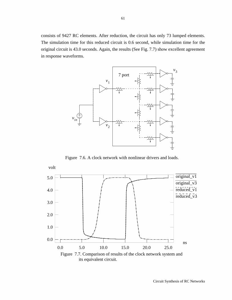
61
Circuit Synthesis of RC Networks
consists of 9427 RC elements. After reduction, the circuit has only 73 lumped elements.
The simulation time for this reduced circuit is 0.6 second, while simulation time for the
original circuit is 43.0 seconds. Again, the results (See Fig. 7.7) show excellent agreement
in response waveforms.
Figure 7.6. A clock network with nonlinear drivers and loads.
vin
v1
v3
v2
7 port
Figure 7.7. Comparison of results of the clock network system andits equivalent circuit.
original_v1
original_v3
reduced_v1
reduced_v3
volt
ns0.0
1.0
2.0
3.0
4.0
5.0
0.0 5.0 10.0 15.0 20.0 25.0

62
A CMOS Driver Model for Transient and Power Dissipation Analysis
CHAPTER 8 A CMOS Driver Model forTransient and PowerDissipation Analysis
Despite the increasing importance of interconnects in transient analysis, nonlinear
active devices in a system also contribute to the system behavior significantly. While most
transient analysis techniques of interconnect networks ignore the nonlinearity of the
driving gates [69, 60], most CMOS driver models do not take into account the distributed
loads [27, 35, 37]. Delay computation of a CMOS driver is based on the assumption that
the output current is only dependent on the lumped load capacitance [27] and the rise time
of the input waveform [35, 37]. A model for the nMOS driver with a lumped capacitive
load is also proposed in [55, 56]. The output waveform is simply characterized as time-
shifted ramps with exponential tails. The static power dissipation is assumed to be roughly
proportional to the ratio of channel width and length. These assumptions will result in
significant error for distributed interconnect loads. A current model of a nonlinear driver is
proposed in [63], where a distributed interconnect load is modeled with summation of
exponential functions. Since using a linearly increasing current source to model
quadratically increasing output current, this model deviates from SPICE results
significantly. All of these driver models ignore transient leakage (short-circuit) current.
When the inverter is slightly loaded, and output rise and fall time are relatively short as
compared to the input rise and fall time, then the short-circuit dissipation will increase to
the same order of magnitude as the dynamic dissipation [76]. Therefore, the analysis of
63
A CMOS Driver Model for Transient and Power Dissipation Analysis
the short-circuit dissipation is important for the low power design.
In this chapter, we present a new CMOS driver model used in conjunction with the
macromodel of interconnect networks for transient and power dissipation analysis. This
model considers the input slope effects, CMOS nonlinear effects and load interconnect
effects. The driver output current is represented by a linear-quadratic-exponential
piecewise model. Based on this model, we can accurately evaluate the CMOS transient
leakage (short-circuit) current and short-circuit power dissipation. The model provides
accuracy comparable to that of SPICE3e2 with one or two orders of magnitude less
computing time.
8.1 Driver Modeling
We propose an efficient nonlinear current model here to match the output current
waveform of a CMOS inverter. By lumping the input and output capacitors of the active
gates into the interconnect networks, we assume that the magnitude of the current flowing
out of a driver at any instant is a function of the input and output voltages of the driver at
that instant. Therefore, the driver is memoryless, and the current being pumped into the
interconnect is well defined.
The response of an arbitrary linear network with distributed-lumped elements can be
efficiently handled by the scattering-parameter-based macromodel paradigm [48, 49]. As
the load of a CMOS inverter, the linear network needs to be analyzed only once. The
voltage response of the nonlinear input current, referred to as , can be expressed in the
frequency domain as
(8.1)
where is the output current of the driver, and the driving-point impedance or
transfer impedance. The corresponding expression in the time domain is
(8.2)
Since can be approximated by a set of exponential functions, or an
exponentially-decayed polynomial function [49], the remaining problem is to develope a
current model to match the output current of the driver.
Let us consider a nonlinear CMOS driver shown in Fig. 8.1(a). We assume the input
voltage to be a falling ramp signal or rising ramp signal. For a falling input voltage
vo
Vo s( ) Z s( )Iout s( )=
Iout s( ) Z s( )
vo t( ) z t( )* iout t( )=
z t( )

64
A CMOS Driver Model for Transient and Power Dissipation Analysis
transition shown in Fig. 8.1(b), the corresponding output current is represented by a five-
section piecewise model.
Section 1: . As illustrated in Figure 8.1(c), the output current of the driver
in this section is equal to zero since the source-gate voltage of the pMOS transistor
( ) is less than its threshold voltage , the pMOS works in the cutoff re-
gion.
Section 2: . As the input voltage decreases, the source to gate voltage of
the pMOS transistor exceeds its threshold voltage, causing it to turn on in saturation.
Thus, the pMOS current increases quadratically in this section [79]. While the nMOS
transistor starts from the linear region, enters saturation and finally, into cutoff region, its
VDD
VDD Vpth–
Ipmax
tpthtr tpl time
time
vin
iout
Figure 8.1. Input voltage transition and the current source model.
(b) Input voltage
(c) pMOS current
vin
voutp
n(a) CMOS driver
VDD
tpx
Ipx
1 2 3 4 5
0 t tpth≤ ≤
VDD vin t( )– Vpth
tpth t tr≤<
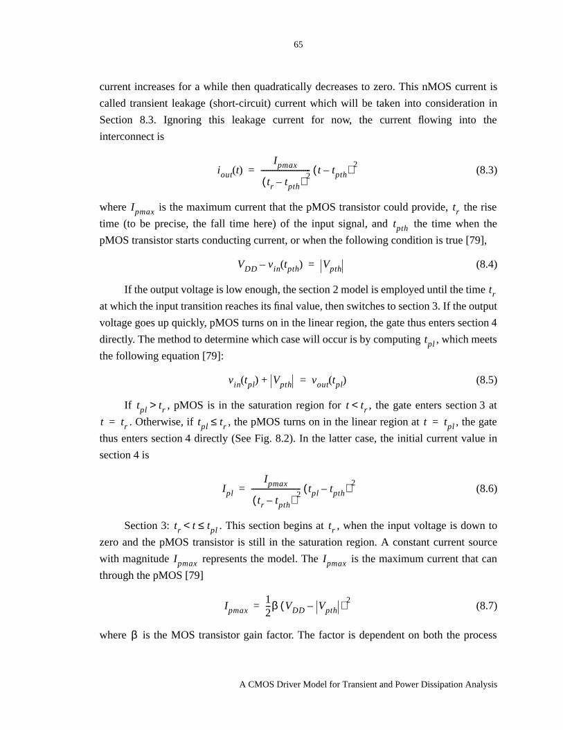
65
A CMOS Driver Model for Transient and Power Dissipation Analysis
current increases for a while then quadratically decreases to zero. This nMOS current is
called transient leakage (short-circuit) current which will be taken into consideration in
Section 8.3. Ignoring this leakage current for now, the current flowing into the
interconnect is
(8.3)
where is the maximum current that the pMOS transistor could provide, the rise
time (to be precise, the fall time here) of the input signal, and the time when the
pMOS transistor starts conducting current, or when the following condition is true [79],
(8.4)
If the output voltage is low enough, the section 2 model is employed until the time
at which the input transition reaches its final value, then switches to section 3. If the output
voltage goes up quickly, pMOS turns on in the linear region, the gate thus enters section 4
directly. The method to determine which case will occur is by computing , which meets
the following equation [79]:
(8.5)
If , pMOS is in the saturation region for , the gate enters section 3 at
. Otherwise, if , the pMOS turns on in the linear region at , the gate
thus enters section 4 directly (See Fig. 8.2). In the latter case, the initial current value in
section 4 is
(8.6)
Section 3: . This section begins at , when the input voltage is down to
zero and the pMOS transistor is still in the saturation region. A constant current source
with magnitude represents the model. The is the maximum current that can
through the pMOS [79]
(8.7)
where is the MOS transistor gain factor. The factor is dependent on both the process
iout t( )Ipmax
tr tpth–( ) 2--------------------------- t tpth–( ) 2
=
Ipmax trtpth
VDD vin tpth( )– Vpth=
tr
tpl
vin tpl( ) Vpth+ vout tpl( )=
tpl tr> t tr<t tr= tpl tr≤ t tpl=
Ipl
Ipmax
tr tpth–( ) 2--------------------------- tpl tpth–( ) 2
=
tr t tpl≤< tr
Ipmax Ipmax
Ipmax12---β VDD Vpth–( ) 2
=
β

66
A CMOS Driver Model for Transient and Power Dissipation Analysis
parameters and the device geometry, and is given by
(8.8)
where is the effective surface mobility of the carriers in the channel, the permittivity
of the gate insulator, the thickness of the gate insulator, the width of the channel,
and the length of the channel. In this case, the initial current of section 4 is .
When the output voltage rises to a value such that pMOS transistor enters its linear
region (See Eq. (8.5)), the output current of the pMOS becomes [79]
(8.9)
where and . Although this region is
commonly called the linear region, varies lineally with only when the
quadratic term is small. Instead of modeling the remaining pMOS current in one
section such as [63], we model this region into two sections.
Section 4: . is the time at which the is a half of the voltage
Figure 8.2. pMOS current when .tpl tr<
VDD
VDD Vpth–
Ipl
tpthtrtpl time
time
vin
iout
(a) Input voltage
(b) pMOS current
tpx
Ipx
Ipmax
1 2 4 5
β µεtox------ W
L-----
=
µ εtox W
L Ipl Ipmax=
iout t( ) β vsg t( ) Vpth–( ) vsd t( ) vsd2
t( ) 2⁄–=
vsg t( ) VDD vin t( )–= vsd t( ) VDD vout t( )–=
iout t( ) vsd t( )
vsd2
t( ) 2⁄
pl t tpx≤< tpx vsd t( )

67
A CMOS Driver Model for Transient and Power Dissipation Analysis
. That is, , or
(8.10)
Thus,
(8.11)
In this section, the output current is a nonlinear function of the output voltage. We
model this output current with a quadratic curve, that is
(8.12)
where is the pMOS output current at . and meet
the DC property (Eq. (8.9)), and the load property (Eq. (8.2)).
Section 5: . When output voltage continuously goes up, the transistor with the
constant input voltage behaves like a linear resistor. The output current is modeled by an
exponential decay function as the output voltage reaches its final value. The time constant
is initially computed based on the charge which has been pumped into the loading net-
work. Since the initial value of the current is known, the exponential decay function is de-
termined solely by its time constant. Assume that output current in this section is
(8.13)
The charge pumped into the interconnect in section 5 is . On the other hand, the
total charge previously pumped into the interconnect in section 1, 2, 3 and 4 is
(8.14)
Thus, if there is no DC path from source to the ground, we can determine the time
constant by
(8.15)
where is the equivalent driving-point capacitance of the interconnect network and
can be computed as the load of the driver by the scattering-parameter-based macromodel.
vsg t( ) Vpth– vsd tpx( ) vsg tpx( ) Vpth–( ) 2⁄=
VDD vout tpx( )– VDD vin tpx( )– Vpth–( ) 2⁄=
vout tpx( ) VDD vin tpx( ) Vpth++( ) 2⁄=
iout t( ) Ipl
Ipl Ipx–
tpx tpl–( ) 2--------------------------- t tpl–( ) 2
–=
Ipx iout tpx( )= t tpx= iout tpx( ) vout tpx( )
t tpx>
τ
iout t( ) Ipxet tpl–( ) τ⁄–
=
Ipxτ
Qprev
13--- 2tpx tpl 2tr– tpth–+( ) Ipmax tpl tr≥( )
13--- 2tpx tpl– tpth–( ) Ipl tpl tr<( )
=
τ
Ipxτ Qprev+ CeqvVDD=
Ceqv
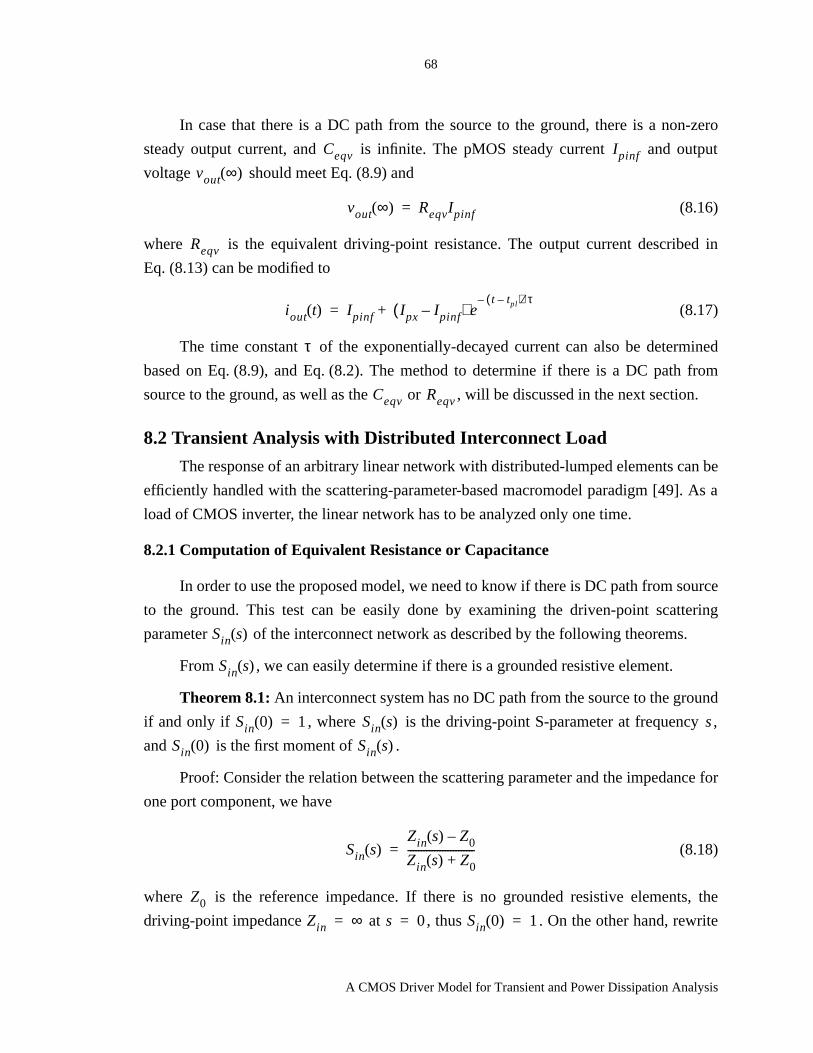
68
A CMOS Driver Model for Transient and Power Dissipation Analysis
In case that there is a DC path from the source to the ground, there is a non-zero
steady output current, and is infinite. The pMOS steady current and output
voltage should meet Eq. (8.9) and
(8.16)
where is the equivalent driving-point resistance. The output current described in
Eq. (8.13) can be modified to
(8.17)
The time constant of the exponentially-decayed current can also be determined
based on Eq. (8.9), and Eq. (8.2). The method to determine if there is a DC path from
source to the ground, as well as the or , will be discussed in the next section.
8.2 Transient Analysis with Distributed Interconnect Load
The response of an arbitrary linear network with distributed-lumped elements can be
efficiently handled with the scattering-parameter-based macromodel paradigm [49]. As a
load of CMOS inverter, the linear network has to be analyzed only one time.
8.2.1 Computation of Equivalent Resistance or Capacitance
In order to use the proposed model, we need to know if there is DC path from source
to the ground. This test can be easily done by examining the driven-point scattering
parameter of the interconnect network as described by the following theorems.
From , we can easily determine if there is a grounded resistive element.
Theorem 8.1:An interconnect system has no DC path from the source to the ground
if and only if , where is the driving-point S-parameter at frequency ,
and is the first moment of .
Proof: Consider the relation between the scattering parameter and the impedance for
one port component, we have
(8.18)
where is the reference impedance. If there is no grounded resistive elements, the
driving-point impedance at , thus . On the other hand, rewrite
Ceqv Ipinf
vout ∞( )
vout ∞( ) ReqvIpinf=
Reqv
iout t( ) Ipinf Ipx Ipinf–( ) et tpl–( ) τ⁄–
+=
τ
Ceqv Reqv
Sin s( )
Sin s( )
Sin 0( ) 1= Sin s( ) s
Sin 0( ) Sin s( )
Sin s( )Zin s( ) Z0–
Zin s( ) Z0+-------------------------=
Z0
Zin ∞= s 0= Sin 0( ) 1=
69
A CMOS Driver Model for Transient and Power Dissipation Analysis
the above equation
(8.19)
If , then , indicating no DC path from the source to the
ground.
Theorem 8.2:For an interconnect system with at least one DC path from the source
to the ground, the equivalent driving-point resistance is
(8.20)
The theorem can be easily proved from Eq. (8.19). This theorem shows that the
equivalent driving-point resistance is only dependent on the first moment of the driving-
point S-parameter.
From the property of Taylor series, the second moment of the is . The
following theorem shows that the equivalent driving-point capacitance is only dependent
on the second moment of .
Theorem 8.3:For an interconnect system with no DC path from the source to the
ground, the equivalent driving-point capacitance is
(8.21)
Proof: From Eq. (8.19), since , there is a pole at for driving-point
impedance. The corresponding residue is
(8.22)
and the equivalent driving-point capacitance is
Consequently, the pole at makes it impossible to express the driving-point
impedance in Taylor series. In this case, the function to be matched with exponential func-
Zin s( )1 Sin s( )+
1 Sin s( )–----------------------Z0=
Sin 0( ) 1= Zin 0( ) ∞=
Reqv Zin 0( )1 Sin 0( )+
1 Sin 0( )–-----------------------Z0= =
Sin s( )sd
dSin 0( )
Sin
Ceqv1
2Z0---------
sdd
Sin 0( )–=
Sin 0( ) 1= s 0=
k01 Sin+( ) Z0
sdd 1 Sin–( )-----------------------------
s 0=
1 Sin 0( )+( ) Z0
sdd
Sin 0( )------------------------------------–
2Z0
sdd
Sin 0( )--------------------–= = =
Ceqv1k0-----
12Z0---------
sdd
Sin 0( )–= =
s 0=

70
A CMOS Driver Model for Transient and Power Dissipation Analysis
tions becomes
(8.23)
These three theorems provide a method to determine if there is a DC path from the
source to the ground, and the means to compute the equivalent driving-point resistance
or the equivalent driving-point capacitance , which are used in the current mod-
el. We have thus completed the construction of the driver model. This new model is an ac-
curate approximation for a wide range of CMOS gates. The next section focuses on how
to combine this driver model with the Padé or Exponentially-Decayed Polynomial Func-
tion (EDPF) approximation of the interconnect for transient analysis.
8.2.2 Transient Analysis
A driver model should be combined with the transfer function of the interconnect
network which is the load of the driver (See Eq. (8.2)). Based on the scattering-parameter-
macromodel, the transfer function in the time domain can be approximated as a summa-
tion of exponentials using Padé technique [48]. A transfer function with -th order Padé
approximation has the following form:
(8.24)
where are the poles and the corresponding residues. The transfer function can also
be approximated as an Exponentially-Decayed Polynomial Function (EDPF) [49]. A
transfer function with -th order EDPF approximation has the following forms:
(8.25)
where is the time constant of the EDPF, the coefficients.
On the other hand, based on the analysis in last section, the output current of a driver
can be expressed as (for )
Z'in Zin1
Ceqvs-------------–=
Reqv Ceqv
q
hp t( ) kiepi t
i 1=
qp
∑=
pi ki
q
he t( ) citd---
i
i 0=
qe
∑ et d⁄( )–
=
d ci
tpl tr≥

71
A CMOS Driver Model for Transient and Power Dissipation Analysis
(8.26)
Similar formulas can also be derived for the other case where . To symboli-
cally convolve the transfer function with output current of the driver , we take each
term in or with each term in . Suppose a quadratic function is
(8.27)
The effect of the quadratic function on an exponential in can be explicitly rep-
resented, for , by
(8.28)
For , it can also be expressed by
(8.29)
The convolution of with input can be computed by recursive formulas. For ex-
ample, the effect of the quadratic input signal on the th order exponentially-decayed
polynomial function for is
iout t( )
0 t tpth≤
Ipmax
tr tpth–( ) 2--------------------------- t tpth–( ) 2
tpth t tr≤<
Ipmax tr t tpl≤<
Ipmax
Ipmax Ipx–
tpx tpl–( ) 2--------------------------- t tpl–( ) 2
– tpl t tpx≤<
Ipinf Ipx Ipinf–( ) et tpl–( ) τ⁄–
+ tpx t<
=
tpl tr<iout t( )
hp t( ) he t( ) iout t( )
f t( )t2
t t0≤
0 t t0>
=
hp t( )
t t0≤
f t( )* kiepi t
ki t
33⁄ pi 0=
ki 2epi t 2– 2pi t– pi
2t2
– pi
3⁄ pi 0≠
=
t t0>
f t( )* kiepi t
ki t0
33⁄ pi 0=
kiepi t 2 2 2pi t0 pi
2t02
+ +( ) ep– i t0–
pi3⁄ pi 0≠
=
he t( )
q
t t0≤
72
A CMOS Driver Model for Transient and Power Dissipation Analysis
(8.30)
where
(8.31)
with and . Based on Eq. (8.30)
and Eq. (8.31), we have a simple algorithm to implement the convolution process:
,
for ( ; ; )
The proof of the algorithm is omitted for brevity. The formulas for , and convo-
lution of or with a step, ramp and exponentially-decaying function can also be
computed by time domain explicit formulas or recursive formulas.
8.3 Power Dissipation Analysis with Transient Leakage Current
Most CMOS driver models ignore transient leakage (short-circuit) current. When the
rise time of the output voltage is comparable to the rise time of the input signal, the leak-
age current become significant, and the corresponding leakage dissipation will be similar
in magnitude as the dynamic dissipation [76]. Previous methods of evaluating the leakage
current are all based on the assumption that the load is a lumped capacitor [35, 76].
In order to accurately estimate the leakage current of the CMOS driver with a gener-
al interconnect load, we analyze the leakage current of the nMOS transistor for the falling
ramp input signal shown in Fig. 8.1. The current through nMOS can be represented by a
Fq t( ) f t( )* he t( )=
cj t2
2td j 1+( )– d2
j 1+( ) j 2+( )+( ) fj t( )j 0=
q
∑ +=
cj td t d j 2+( )–( ) td---
je
t d⁄–
j 0=
q
∑
fj t( )τd---
je
τ d⁄–dτ
0
t
∫=
fj t( ) jf j 1– t( ) d t d⁄( ) je
t d⁄––= f0 t( ) d 1 e
t d⁄––( )=
value 0← K 0←
j order← j 0≥ j j 1–←
K j 1+( ) K cj t2
2td j 1+( )– d2
j 1+( ) j 2+( )+( )+←
value value t d⁄× cj td t d j 2+( )–( ) d K×–+←
value value et d⁄–× d K×+←
t t0>hp t( ) he t( )

73
A CMOS Driver Model for Transient and Power Dissipation Analysis
four-section piecewise model (See Fig. 8.3).
Section 1: . Here equals zero since and output voltage are zero.
Section 2: . As the pMOS transistor turns in the saturation region and
output voltage increases, the nMOS goes into linear region. In this section, input voltage
goes down linearly and output voltage increases nonlinearly. We use a quadratically in-
creasing current source to model the nMOS nonlinearly increasing current. This section is
employed until the nMOS enters to the saturation region at , where is the time that
input voltage and output voltage meet the following condition:
(8.32)
So, the nMOS current in this section is
(8.33)
where is determined by and , the maximum current that the nMOS can
Figure 8.3. pMOS current and nMOS current (leakage current) .ip in
(a) Input voltage
(b) Output currentip
in
VDD
VDD Vpth–
Ipmax
tpth tr tpl time
time
vin
iout
tpx
Inmax
tns tnth
Ins
Vnth
1 2
3
4
t tpth≤ in ip
tpth t tns≤<
tns tns
vin tns( ) vnth– vout tns( )=
in t( )Ins
tns tpth–( ) 2----------------------------- t tpth–( ) 2
=
Ins tns Inmax

74
A CMOS Driver Model for Transient and Power Dissipation Analysis
supply.
Section 3: . As the nMOS switches to the saturation region, the current
quadratically decreases. This process continues until the current dies down to zero at ,
when the nMOS goes into the cutoff region. The current in this region can be expressed by
(8.34)
Note that
(8.35)
Section 4: . In this section, the nMOS is in the cutoff region, its current is ze-
ro.
Overall, the current through the nMOS can be expressed as
(8.36)
The convolution formula we have derived early can also be used here. All charges
go through nMOS transistor are
(8.37)
Thus, the short-circuit power dissipation for this transient change is
(8.38)
8.4 Experimental Results
The proposed driver models were tested on several circuits using SUN SPARC 1+
workstation.
tns t tnth≤<tnth
in t( )Inmax
tnth2
------------ tnth t–( ) 2=
Ins
Inmax
tnth2
------------ tnth tns–( ) 2=
t tnth>
in t( )
Ins
tns tpth–( ) 2----------------------------- t tpth–( ) 2
tpth t tns≤<
Inmax
tnth2
------------ tnth t–( ) 2tns t tnth≤<
0 otherwise
=
Qnprev in t( ) td∫Ins
3------ tnth tpth–( )= =
Ws VDDQnprev
VDDIns
3----------------- tnth tpth–( )= =
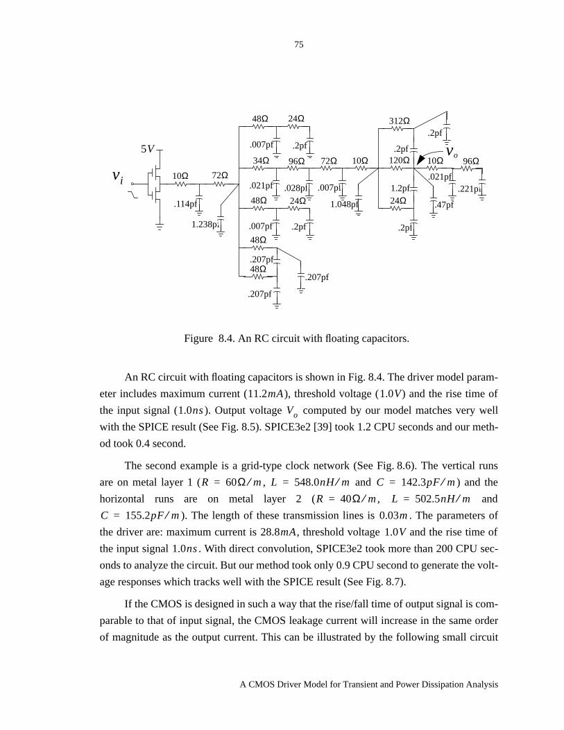
75
A CMOS Driver Model for Transient and Power Dissipation Analysis
An RC circuit with floating capacitors is shown in Fig. 8.4. The driver model param-
eter includes maximum current ( ), threshold voltage ( ) and the rise time of
the input signal ( ). Output voltage computed by our model matches very well
with the SPICE result (See Fig. 8.5). SPICE3e2 [39] took 1.2 CPU seconds and our meth-
od took 0.4 second.
The second example is a grid-type clock network (See Fig. 8.6). The vertical runs
are on metal layer 1 ( , and ) and the
horizontal runs are on metal layer 2 ( , and
). The length of these transmission lines is . The parameters of
the driver are: maximum current is , threshold voltage and the rise time of
the input signal . With direct convolution, SPICE3e2 took more than 200 CPU sec-
onds to analyze the circuit. But our method took only 0.9 CPU second to generate the volt-
age responses which tracks well with the SPICE result (See Fig. 8.7).
If the CMOS is designed in such a way that the rise/fall time of output signal is com-
parable to that of input signal, the CMOS leakage current will increase in the same order
of magnitude as the output current. This can be illustrated by the following small circuit
72Ω10Ω
.114pf
1.238pf
48Ω
48Ω
.207pf
.207pf
48Ω 24Ω
.007pf .2pf
48Ω 24Ω
.007pf .2pf
34Ω 96Ω 72Ω
.021pf .028pf .007pf
10Ω
312Ω
120Ω
24Ω1.2pf
.2pf
.2pf
.2pf
10Ω 96Ω
.221pf.021pfvi
1.048pf .47pf
vo5V
Figure 8.4. An RC circuit with floating capacitors.
.207pf
11.2mA 1.0V
1.0ns Vo
R 60Ω m⁄= L 548.0nH m⁄= C 142.3pF m⁄=
R 40Ω m⁄= L 502.5nH m⁄=
C 155.2pF m⁄= 0.03m
28.8mA 1.0V
1.0ns
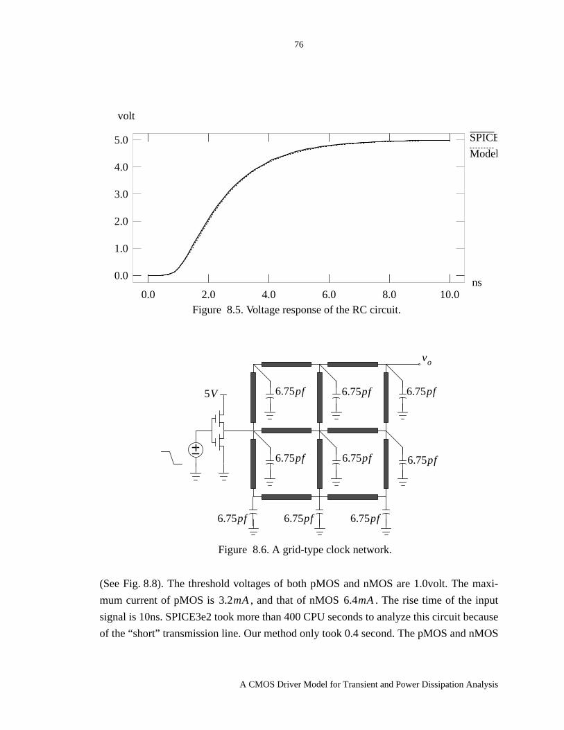
76
A CMOS Driver Model for Transient and Power Dissipation Analysis
(See Fig. 8.8). The threshold voltages of both pMOS and nMOS are 1.0volt. The maxi-
mum current of pMOS is , and that of nMOS . The rise time of the input
signal is 10ns. SPICE3e2 took more than 400 CPU seconds to analyze this circuit because
of the “short” transmission line. Our method only took 0.4 second. The pMOS and nMOS
Figure 8.5. Voltage response of the RC circuit.
SPICE
Model
volt
ns0.0
1.0
2.0
3.0
4.0
5.0
0.0 2.0 4.0 6.0 8.0 10.0
5V
6.75pf 6.75pf
6.75pf 6.75pf
6.75pf6.75pf
vo
6.75pf
6.75pf
6.75pf
Figure 8.6. A grid-type clock network.
3.2mA 6.4mA

77
A CMOS Driver Model for Transient and Power Dissipation Analysis
currents are shown in Fig. 8.9. The steady output current is not equal zero because there is
a DC path from source to ground. Obviously, if we ignored the nMOS current (leakage
current), it would create quite large error. The voltage response is shown in Fig. 8.10.
Finally, we demonstrate the efficiency of the driver model by evaluating a large in-
dustry circuit. The circuit, driven by a CMOS inverter, includes 2895 resistors, 2767 ca-
pacitors and 73 lossy transmission lines. SPICE3e2 [39] took more than 5200 seconds to
analyze the circuit and our method took 86.5 seconds. The voltage response is shown in
Fig. 8.11.
Figure 8.7. Voltage response of the clock network.
SPICE
Model
volt
ns0.0
1.0
2.0
3.0
4.0
5.0
0.0 20.0 40.0 60.0 80.0
Figure 8.8. A transmission line circuit with a DC path from source to ground.
5V
0.1pf5kΩ
1.0mm
R=0.2Ω/cmL=1.667nH/cmC=1.852pf/cm vout
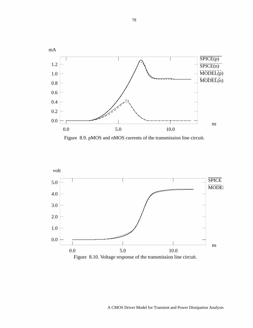
78
A CMOS Driver Model for Transient and Power Dissipation Analysis
Figure 8.9. pMOS and nMOS currents of the transmission line circuit.
SPICE(p)
SPICE(n)
MODEL(p)
MODEL(n)
mA
ns0.0
0.2
0.4
0.6
0.8
1.0
1.2
0.0 5.0 10.0
Figure 8.10. Voltage response of the transmission line circuit.
SPICE
MODEL
volt
ns0.0
1.0
2.0
3.0
4.0
5.0
0.0 5.0 10.0

79
A CMOS Driver Model for Transient and Power Dissipation Analysis
Figure 8.11. Voltage response of a large clock network.
SPICE
Model
volt
ns0.0
0.5
1.0
1.5
2.0
2.5
3.0
3.5
0.0 2.0 4.0 6.0 8.0 10.0
80
Conclusions
CHAPTER 9 Conclusions
9.1 Concluding Remarks
The scattering-parameter-based macromodel provides an efficient method and
strategy to analyze interconnect networks. Lossy transmission lines, floating capacitors
and inductors, capacitive or inductive cutsets and loops are all easily addressed with the
macromodel. Time-of-flight delay of transmission line networks can be explicitly
captured, which greatly improves the accuracy of the macromodel. Large interconnect
networks with large number of external ports or nonlinear terminations are easily dealt
with by efficiently combining circuit reduction and partition. Circuit partitioning speeds
up the reduction process, decreases the simulation time and achieves high accuracy using
lower order approximation. Accuracy can be controlled by adjusting the circuit element
number in each subnetwork. The interconnect networks with nonlinear terminations can
be analyzed with recursive convolution techniques or by synthesizing the reduced
networks. Because of its generality, the macromodel can be used for interconnect analysis
on integrated circuit chips, multichip modules and printed circuit boards. Since no
assumption is made regarding port voltages and currents, the proposed macromodel can be
applied to the simulation of analog circuits and mixed-signal circuits. In conjunction with
the macromodel, the proposed CMOS driver model, which takes into account the input
slope effects, CMOS nonlinear effects, and load interconnect effects, can be used for
event-driven timing analysis and power dissipation analysis for large digital circuits.
81
Conclusions
9.2 Future Research
A number of open theoretical and practical questions are raised as the results of this
thesis research.
The scattering-parameter-based macromodel has been extended to analyze
sensitivity of interconnect networks [75]. The sensitivity and time-of-flight can be kept
during network reduction. The technique that keeps the track of information of time-of-
flight and sensitivity during reduction can be used to merge all linear independent sources,
that is, the ports which are connected to those sources need not to be kept external. The
method will be useful for large circuits with multiple sources, for example, the power and
ground planes where all sources and drains of CMOS transistors are modelled as current
sources, and for the circuits with initial conditions which may exist in the form of static
charge during the idle-period of logic switching and the fetch/store transition period of
memory circuits [17]. Such cases are often ignored in the transient simulations of large
interconnect networks.
Although Padé approximation provides a feasible and accurate model for RC
circuits, it tends to yield unstable poles when the number of poles (order of
approximation) exceeds seven. We have introduced mixed-exponential functions to deal
this problem. However, extremely ill-conditioned matrices because of the severe
numerical problems may still exist when computing high order moments. The complex
frequency hopping method [22] and the PVL (Padé approximation via the Lanczos
process) [29] help to compute high order moments by avoiding the ill-condition problem.
However, difficulty of determining approximation order with moment matching technique
hinders their use. In addition, increasing the approximation order will increase the
modeling and simulation time. Partitioning and reduction is a feasible solution. We have
proposed an efficient partitioning method to speed up the reduction and simulation.
Efficient data modeling beyond moment matching methods still to be developed.
Scattering-parameter-based macromodel can compute S-matrix at sampling frequency
points [50]. Although least-squares, which can compute the error norm of approximation
[74], could be used, a more robust data modeling technique is needed to avoid numerical
problems when the number of poles goes larger. Linear system identification technique
[71] could be one of choices.
Approximating the multiport macromodel is another open question. The more strict
requirement that the reduced model is stable must impose the approximation process. This

82
Conclusions
requirement includes testing bounded-real condition of the reduced network scattering
matrix and avoiding non-bounded-real results.
The most outstanding open problem in circuit synthesis is to synthesize multiport
reciprocal networks without the use of transformers [58]. We have presented a lower order
RC synthesis of interconnect networks with RC elements. The synthesized circuits are
always stable. The technique may be extended to handle RLC circuits and transmission
line networks where there are time-of-flight delays between some pairs of ports.

83
Scattering Matrix of an Ideal Interconnect Node
Appendix A Scattering Matrix of an IdealInterconnect Node
For each vertex corresponding to an interconnect node (Figure A.1), Kirchoff’s
voltage law and current law hold. For the port interconnect node, we have
(A.1)
(A.2)
Figure A.1. An ideal interconnect node.
aibn
bi
b2
b1
a2
Vn
an
a1
In
I i
I2
I1
Vi
V2
V1
n
V1 V2 … Vn= = =
I1 I2 … In+ + + 0=
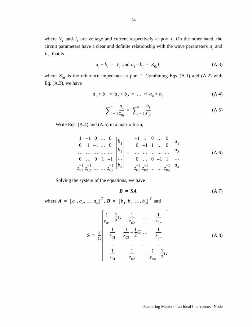
84
Scattering Matrix of an Ideal Interconnect Node
where and are voltage and current respectively at port . On the other hand, the
circuit parameters have a clear and definite relationship with the wave parameters and
, that is
and (A.3)
where is the reference impedance at port . Combining Eqs. (A.1) and (A.2) with
Eq. (A.3), we have
(A.4)
(A.5)
Write Eqs. (A.4) and (A.5) in a matrix form,
(A.6)
Solving the system of the equations, we have
(A.7)
where , and
(A.8)
Vi I i i
ai
bi
ai bi+ Vi= ai bi– Z0i I i=
Z0i i
a1 b1+ a2 b2+ … an bn+= = =
ai
z0i------
i 1=
n∑bi
z0i------
i 1=
n∑=
1 1– 0 … 0
0 1 1– … 0
… … … … …0 … 0 1 1–
z011–
z021– … … z0n
1–
b1
b2
…bn
1– 1 0 … 0
0 1– 1 … 0
… … … … …0 … 0 1– 1
z011–
z021– … … z0n
1–
a1
a2
…an
=
B SA=
A a1 a2 … an, , ,[ ] T= B b1 b2 … bn, , ,[ ] T
=
S2G----
1z01-------
12---G–
1z02------- … 1
z0n-------
1z01------- 1
z02-------
12---G– … 1
z0n-------
… … … …1
z01------- 1
z02------- … 1
z0n-------
12---G–
=

85
Scattering Matrix of an Ideal Interconnect Node
where
(A.9)
If all reference impedances are same, that is, , then
(A.10)
The S-matrix of Eq. (A.8) or Eq. (A.10) has some properties [46]. Since
for and , we have
Theorem A.1:The junction vertices contain no preferred voltage wave ports; that is,
outgoing waves at all other ports due to the incoming wave at one port are equal.
For example, if port 1 has an incoming wave and other ports are perfectly
matched (no incoming wave), outgoing waves on all ports other than port 1 are equal to
.
The is called the reflection factor at port . We say the port is perfectly matched
(no reflection) if .
Theorem A.2: If a junction vertex has degree greater than or equal to three, it is
impossible for all its ports to be perfectly matched. That is, it is impossible that
for if .
Proof: Assume that all ( ) for a junction vertex, that is,
(A.11)
Since , we can rewrite Eq. (A.11) as:
(A.12)
G1z0i------
i 1=
n∑=
z01 z02 … z0n= = =
S1n---
2 n– 2 … 2
2 2 n– … 2
… … … …2 2 … 2 n–
=
Sik Sjk=
i k≠ j k≠
a1
2G1–z01
1–a1
Sii i i
Sii 0=
Sii 0=
i 1 2 … n, , ,= n 3≥
Sii 0= i 1 2 … n, , ,=
2Gz0i----------- 1– 0= i 1 2 … n, , ,=
G 0≠
2z0i------ G– 0= i 1 2 … n, , ,=
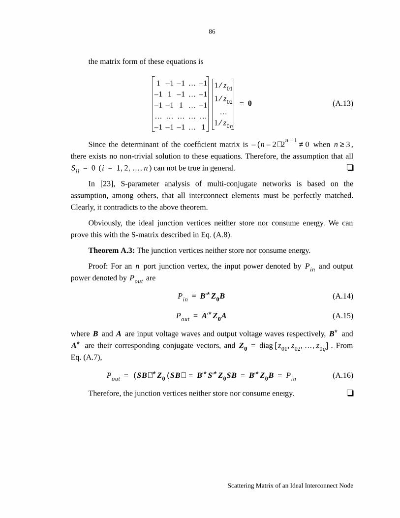
86
Scattering Matrix of an Ideal Interconnect Node
the matrix form of these equations is
(A.13)
Since the determinant of the coefficient matrix is when ,
there exists no non-trivial solution to these equations. Therefore, the assumption that all
( ) can not be true in general.
In [23], S-parameter analysis of multi-conjugate networks is based on the
assumption, among others, that all interconnect elements must be perfectly matched.
Clearly, it contradicts to the above theorem.
Obviously, the ideal junction vertices neither store nor consume energy. We can
prove this with the S-matrix described in Eq. (A.8).
Theorem A.3:The junction vertices neither store nor consume energy.
Proof: For an port junction vertex, the input power denoted by and output
power denoted by are
(A.14)
(A.15)
where and are input voltage waves and output voltage waves respectively, and
are their corresponding conjugate vectors, and . From
Eq. (A.7),
(A.16)
Therefore, the junction vertices neither store nor consume energy.
1 1– 1– … 1–
1– 1 1– … 1–
1– 1– 1 … 1–
… … … … …1– 1– 1– … 1
1 z01⁄
1 z02⁄
…1 z0n⁄
0=
n 2–( ) 2n 1–
– 0≠ n 3≥
Sii 0= i 1 2 … n, , ,=
n Pin
Pout
Pin B'∗Z0B=
Pout A'∗Z0A=
B A B∗
A∗ Z0 diag z01 z02 … z0q, , ,[ ]=
Pout SB( ) '∗Z0 SB( ) B'∗S'∗Z0SB B'∗Z0B Pin= = = =
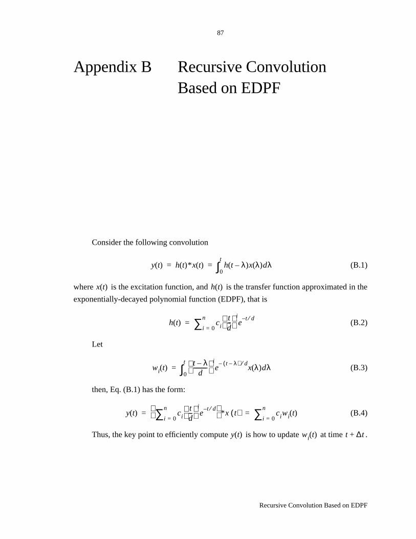
87
Recursive Convolution Based on EDPF
Appendix B Recursive ConvolutionBased on EDPF
Consider the following convolution
(B.1)
where is the excitation function, and is the transfer function approximated in the
exponentially-decayed polynomial function (EDPF), that is
(B.2)
Let
(B.3)
then, Eq. (B.1) has the form:
(B.4)
Thus, the key point to efficiently compute is how to update at time .
y t( ) h t( )* x t( ) h t λ–( )x λ( )dλ0
t
∫= =
x t( ) h t( )
h t( ) citd---
ie
t d⁄–
i 0=
n∑=
wi t( )t λ–
d----------
ie
t λ–( ) d⁄–x λ( )dλ
0
t
∫=
y t( ) citd---
ie
t d⁄–
i 0=
n∑ * x t( ) ciwi t( )
i 0=
n∑= =
y t( ) wi t( ) t ∆t+
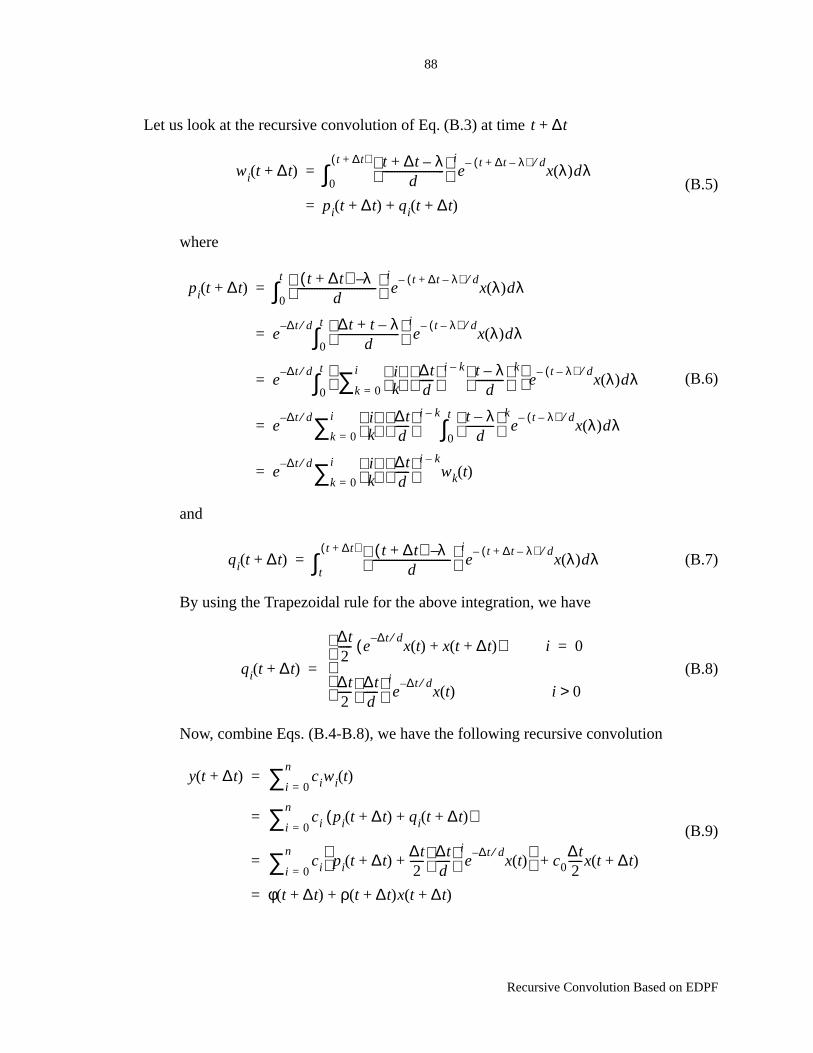
88
Recursive Convolution Based on EDPF
Let us look at the recursive convolution of Eq. (B.3) at time
(B.5)
where
(B.6)
and
(B.7)
By using the Trapezoidal rule for the above integration, we have
(B.8)
Now, combine Eqs. (B.4-B.8), we have the following recursive convolution
(B.9)
t ∆t+
wi t ∆t+( )t ∆t+ λ–
d-----------------------
ie
t ∆t+ λ–( ) d⁄–x λ( )dλ
0
t ∆t+( )∫=
pi t ∆t+( ) qi t ∆t+( )+=
pi t ∆t+( )t ∆t+( ) λ–
d-----------------------------
ie
t ∆t+ λ–( ) d⁄–x λ( )dλ
0
t
∫=
e∆t d⁄– ∆t t λ–+
d-----------------------
ie
t λ–( ) d⁄–x λ( )dλ
0
t
∫=
e∆t d⁄– i
k ∆t
d-----
i k– t λ–d
---------- k
k 0=
i∑ e
t λ–( ) d⁄–x λ( )dλ
0
t
∫=
e∆t d⁄– i
k ∆t
d-----
i k– t λ–d
---------- k
et λ–( ) d⁄–
x λ( )dλ0
t
∫k 0=
i∑=
e∆t d⁄– i
k ∆t
d-----
i k–wk t( )
k 0=
i∑=
qi t ∆t+( )t ∆t+( ) λ–
d-----------------------------
ie
t ∆t+ λ–( ) d⁄–x λ( )dλ
t
t ∆t+( )∫=
qi t ∆t+( )
∆t2----- e
∆t d⁄–x t( ) x t ∆t+( )+( ) i 0=
∆t2----- ∆t
d-----
ie
∆t d⁄–x t( ) i 0>
=
y t ∆t+( ) ciwi t( )i 0=
n∑=
ci pi t ∆t+( ) qi t ∆t+( )+( )i 0=
n∑=
ci pi t ∆t+( )∆t2----- ∆t
d-----
ie
∆t d⁄–x t( )+
i 0=
n∑ c0∆t2-----x t ∆t+( )+=
φ t ∆t+( ) ρ t ∆t+( )x t ∆t+( )+=

89
Recursive Convolution Based on EDPF
where and can be computed with the following recursive
formulas:
(B.10)
ρ t ∆t+( ) c0∆t 2⁄= φ t ∆t+( )
φ t ∆t+( ) ciζi t ∆t+( )i 0=
n∑=
ζi t ∆t+( ) e∆t d⁄– i
k ∆t
d-----
i k–wk t( )
k 0=
i∑ ∆t2----- ∆t
d-----
ix t( )+
=
wk t ∆t+( ) ζk t ∆t+( )∆t2-----x t ∆t+( )+=
90
References
References
[1] D. F. Anastasakis, N. Gopal, S.-Y. Kim and L. T. Pillage, “Enhancing the Stability of
Asymptotic Waveform Evaluation for Digital Interconnect Circuit Applications,”
IEEE Transactions on Computer-Aided Design of Integrated Circuits and Systems,
pp. 729-736, June 1994.
[2] B. D. O. Anderson and S. Vongpanitlerd,Network Analysis and Synthesis: A Modern
Systems Theory Approach, Englewood Cliffs, N.J., Prentice-Hall, 1973.
[3] G. A. Baker, Jr. and J. L. Gammel,The Padé Approximant in Theoretical physics,
New York, Academic Press, 1970.
[4] G. A. Baker, Jr. and P. Graves-Morris,Padé Approximants, Part I: Basic Theory,
Mass.: Addison-Wesley, 1981.
[5] G. A. Baker, Jr. and P. Graves-Morris,Padé Approximants, Part II: Extensions and
Applications, Mass.: Addison-Wesley, 1981.
[6] N. Balabanian, T. A. Bickart,Electrical Network Theory, ch. 6, Malabar, Florida:
Robert E. Krieger, 1985.
[7] L. Barford, B. Troyanovsky, N. H. Chang, H. Liao and W. Dai, “System Identification
Techniques for Fast, Recursive Convolution Based Circuit Simulation for Large RC
Circuits,” Proceedings of HP Design Technology Conference, 1995.
[8] A. Belantari, “Error Estimate in Vector Padé Approximation,”Applied Numerical
Mathematics, pp. 457-468, 1991.
91
References
[9] J. E. Bracken, V. Raghavan, and R. A. Rohrer, “Simulating Distributed Elements with
Asymptotic Waveform Evaluation,”IEEE MTT-S International Microwave Sympo-
sium Digest,pp. 1337-1340, 1992.
[10] J. E. Bracken, V. Raghavan, and R. A. Rohrer, “Extension of the Asymptotic Wave-
form Evaluation Technique with the Method of Characteristics,” Technical Digest of
the IEEE International Conference on Computer-Aided Design, pp. 71-75, Nov.
1992.
[11] C. Brezinski, “Error Estimate in Padé Approximation,”Proceedings of International
Symposium on Orthogonal Polynomials and their Applications, pp. 1-19, 1988.
[12] C. Brezinski, “Procedures for Estimating the Error in Padé Approximation,” Mathe-
matics of Computation, pp. 639-648, Oct., 1989.
[13] C. Brezinski,History of Continued Fractions and Padé Approximants, New York:
Springer-Verlag, c1991.
[14] H. Cabannes,Padé Approximants Method and Its Applications to Mechanics, New
York: Springer-Verlag, 1976.
[15] P. Chan, M. Schlag, “Bounds on Signal Delay in RC Mesh Networks,”IEEE Trans.
on CAD, Vol. CAD-8, no. 6, June 1989. pp. 581-589
[16] P. Chan, “Comments on ‘Asymptotic Waveform Evaluation for Timing Analysis’,”
IEEE Trans. on CAD, Aug. 1991, pp. 1078-1079.
[17] F. Y. Chang, “Transient Analysis of Lossy Transmission Lines with Arbitrary Initial
Potential and Current Distributions,” IEEE Trans. on Circuits and Systems, vol.
CAS-39, pp. 180-198, March 1991.
[18] F. Y. Chang, “Waveform Relaxation Analysis of Nonuniform Lossy Transmission
Lines Characterized with Frequency-Dependent Parameters,”IEEE Trans. on Cir-
cuits and Systems, vol. CAS-38, pp. 1484-1500, Dec. 1991.
[19] F. Y. Chang, “Transient Simulation of Nonuniform Coupled Lossy Transmission
Lines Characterized with Frequency-Dependent Parameters, Part II: Discrete-Time
Analysis,” IEEE Trans. on Circuits and Systems, vol. CAS-39, pp. 907-927, Nov.
1992.
92
References
[20] H. S. Chen and E.F. Thompson,Iterative and Padé Solutions for the Water-Wave Dis-
persion Relation, National Technical Information Service, 1985.
[21] E. Chiprout and M. Nakhla, “Generalized Moment-matching Methods for Transient
Analysis of Interconnect Networks,”29 th ACM/IEEE Design Automation Confer-
ence Proceedings, 1992. pp. 201-206.
[22] E. Chiprout and M.S. Nakhla, “Analysis of Interconnect Networks Using Complex
Frequency Hopping (CFH),”IEEE Transactions on Computer-Aided Design of Inte-
grated Circuits and Systems, pp. 186-200, Feb. 1995.
[23] B. J. Cooke, J. L. Prince and A. C. Cangellaris, “S-Parameter Analysis of Multicon-
ductor, Integrated Circuit Interconnect Systems,”IEEE Transaction on Computer-
Aided Design,vol. CAD-11(3), pp. 353-360, 1992.
[24] J. K. Cullum and R. A. Willoughby,Lanczos algorithms for large symmetric eigen-
value computations, Boston: Birkhauser, 1985.
[25] T. Dhaene, L. Martens, and D. De Zutter, “Transient Simulation of Arbitrary Nonuni-
form Interconnection Structures Characterized by Scattering Parameters,”IEEE
Trans. on Circuits and Systems, vol. CAS-39, pp. 928-937, Nov. 1992.
[26] J. Dobrowolski,Introduction to Computer Methods for Microwave Circuit Analysis
and Design, Artech House, 1991.
[27] M. I. Elmasry,Digital MOS Integrated Circuits, New York: IEEE Press, pp. 4-27,
1981.
[28] W. C. Elmore, “The Transient Response of Damped Linear Networks with Particular
Regard to Wideband Amplifier,”J. Applied Physics, 19(1), 1948.
[29] P. Feldmann and R. W. Freund, “Efficient Linear Circuit Analysis by Padé Approxi-
mation via the Lanczos Process,”IEEE Transactions on Computer-Aided Design of
Integrated Circuits and Systems, pp. 639-649, May 1995.
[30] P. Feldmann and R. W. Freund, “Reduced-Order Modeling of Large Linear Subcir-
cuits via a Block Lanczos Algorithm,”Proceedings of the 32th ACM/IEEE Design
Automation Conference, June 1995.
93
References
[31] C. M. Fiduccia and R. M. Mattheyses, “A Linear-Time Heuristic Improving Network
Partitions,” Proceedings of the 19th Design Automation Conference, pp. 241-247,
1982.
[32] D. S. Gao, A. T. Yang, and S. M. Kang, “Accurate Modeling and Simulation of Paral-
lel Interconnection in High-speed Integrated circuits,”IEEE Trans. on Circuits and
Systems, pp. 1-9, Jan. 1992.
[33] K. Glover, “All Optimal Hankel-norm Approximations of Linear Multivariable Sys-
tems and Their -error bounds,”Int. J. Control, pp. 1115-1193, 1984.
[34] K. C. Gupta, R. Grag, and R. Chadha,Computer Aided Design of Microwave Cir-
cuits, Dedham, MA: Artech 1981.
[35] N. Hedenstierna, and K. O. Jeppson, “CMOS Circuit Speed and Buffer Optimiza-
tion,” IEEE Trans. on CAD, pp. 270-281, March 1987.
[36] Hewlett-Packard. Application Note 117-1, 1969.
[37] B. Hoppe, G. Neuendorf, D. Schmitt-Landsiedel, and W. Specks, “Optimization of
High-Speed CMOS Logic Circuits with Analytical Models for Signal Delay, Chip
Area, and Dynamic Power Dissipation,”IEEE Trans. on CAD, pp. 236-246, March
1990.
[38] C. Hwang and Y.-C. Lee, “Multifrequency Padé Approximation via Jordan Contin-
ued-Fraction Expansion,”IEEE Transactions on Automatic Control, pp. 444-446,
April 1989.
[39] B. Johnson, T. Quarles, A. R. Newton, D. O. Pederson and A. Sangiovanni-Vincen-
telli, “SPICE3 Version 3e User’s Manual,” University of California, Berkeley, April
1991.
[40] S. Karni,Network Theory: Analysis and Synthesis, Allyn and Bacon, Inc., 1966.
[41] S.-Y. Kim, N. Gopal and L. T. Pillage, “Time-domain Macromodels for VLSI Inter-
connect Analysis,”IEEE Transactions on Computer-Aided Design of Integrated Cir-
cuits and Systems, pp. 1257-70, Oct. 1994.
[42] A. S. Kronrod, “Nodes and Weights of Quadrature Formulas,”Consultant Bureau,
New York, 1965.
L∞
94
References
[43] N. Kuhn, “Simplified Signal Flow Graph Analysis,”Microwave J., VI, No. 11, pp.
59-66, 1963.
[44] P. Lancaster,Theory of Matrices, New York, Academic Press, 1969.
[45] C. Lanczos, “An iteration method for the solution of the eigenvalue problem of linear
differential and integral operators,” J. Res. Nat. Bur. Standards, vol. 45, pp. 255-282,
1950.
[46] H. Liao and W. Dai, “Wave Spreading Evaluation of Interconnect Systems,”Pro-
ceedings of the 3rd IEEE Multichip-module Conference, pp. 128-133, 1993.
[47] H. Liao and W. Dai, “Wave Spreading Evaluation of Interconnect Systems,” Accept-
ed byIEEE Transactions on Microwave Theory and Techniques.
[48] H. Liao, R. Wang, R. Chandra, and W. Dai, “S-Parameter Based Macro Model of Dis-
tributed-Lumped Networks Using Padé Approximation,”IEEE International Sympo-
sium on Circuits and Systems, pp. 2319-2322, May 1993.
[49] H. Liao, W. Dai, R. Wang, and F. Y. Chang, “S-Parameter Based Macro Model of
Distributed-Lumped Networks Using Exponentially Decayed Polynomial Function,”
Proceedings of 30th ACM/IEEE Design Automation Conference, pp. 726-731, June
1993.
[50] H. Liao, W. Dai, “Scattering Parameter Transient Analysis of Interconnect Networks
with Nonlinear Terminations Using Recursive Convolution,”Proceedings of the Syn-
thesis and Simulation Meeting and International Interchange, pp. 295-304, Oct.
1993.
[51] H. Liao, R. Wang, and W. Dai, “Transient Analysis of Interconnects with Nonlinear
Driver Using Mixed Exponential Function Approximation,”Technical Report of Uni-
versity of California at Santa Cruz, UCSC-CRL-93-44, Oct. 1993.
[52] H. Liao, and W. Dai, “Capturing Time-of-Flight Delay for Transient Analysis Based
on Scattering Parameter Macromodel,”IEEE/ACM International Conference on
Computer-Aided Design, pp. 412-417, 1994.
[53] T. Lin, C. Mead, “Signal Delay in General RC networks,”IEEE Trans. on CAD, Vol.
CAD-3, no. 4, pp. 331-349, Oct. 1984.

95
References
[54] S. Lin, and E. S. Kuh, “Transient Simulation of Lossy Interconnects Based on the Re-
cursive Convolution Formulation,”IEEE Trans. on Circuits and Systems, vol. CAS-
39, pp. 879-892, Nov. 1992.
[55] M. D. Matson, “Macromodeling of Digital MOS VLSI Circuits,”Proceedings of 22th
ACM/IEEE Design Automation Conference, pp. 144-151, 1985.
[56] M. D. Matson and L. A. Glasser, “Macromodeling and Optimization of Digital MOS
VLSI Circuits,” IEEE Trans. on CAD, Vol. CAD-5, no. 4, pp. 659-678, Oct. 1986.
[57] V. A. Monaco, and P. Tiberio, “Automatic Scattering Matrix Computation of Micro-
wave Circuits,”Alta Frequenza, vol. 39, pp. 59-64, 1970.
[58] R. W. Newcomb,Linear Multiport Synthesis, New York, McGraw-Hill, 1966.
[59] P. R. O’Brien, T. Savarino, “Modeling the Driving-Point Characteristic of Resistive
Interconnect for Accurate Delay Estimation,”Digest of Technical Papers, ICCAD-
89, Santa Clara, pp. 512-515.
[60] L. T. Pillage, and R. A. Rohrer, “Asymptotic Waveform Evaluation for Timing Anal-
ysis,” IEEE Trans. on CAD, vol. CAD-9, pp. 352-366, April 1990.
[61] A. Pozzi,Application of Padé Approximation Theory in Fluid Dynamics, N.J.: World
Scientific, 1994.
[62] W. H. Press, B. P. Flannery, S. A. Teukolsky, and W. T. Vetterling,Numerical Recipes
in C: The Art of Scientific Computing, Cambridge, June 1991.
[63] V. Raghavan, and R. A. Rohrer, “A New Nonlinear Driver Model for Interconnect
Analysis,”Proceedings of 28th ACM/IEEE Design Automation Conference, pp. 561-
566, 1991.
[64] V. Raghavan, J. E. Bracken, and R. A. Rohrer, “AWESpice: A General Tool for the
Efficient and Accurate Simulation of Interconnect Problems,”Proceedings of 29th
ACM/IEEE Design Automation Conference, pp. 87-92, June 1992.
[65] C. Ratzlaff, N. Gopal, and L. Pillage, “RICE: Rapid Interconnect Circuit Evaluator,”
28th ACM/IEEE Design Automation Conference Proceedings, 1991. pp. 555-560.
[66] J. C. Rautio, “Synthesis of Lumped Models from N-Port Scattering Parameter Data,”
IEEE Transactions Microwave Theory and Techniques, vol. 42, pp. 535-537, March
1994.
96
References
[67] P. A. Rizzi,Microwave Engineering, Englewood Cliffs, NJ. Prentice-Hall, 1988.
[68] J. K. Roberge,Operational Amplifiers: Theory and Practice, John Wiley & Sons Inc.,
pp. 530, 1975.
[69] J. Rubinstein, P. Penfield, and M. Horowitz, “Signal Delay in RC Tree Networks,”
IEEE Trans. On CAD, Vol. CAD-2, no. 3, pp. 202-211, July 1983.
[70] J. S. Roychowdbury, and D. O. Pederson, “Efficient Transient Simulation of Lossy
Interconnect,”Proceedings of 29th ACM/IEEE Design Automation Conference, pp.
740-745, 1992.
[71] J. Schoukens and R. Pintelon,Identification of Linear Systems: A Practical Guidline
to Accurate Modeling, New York: Pergamon Press, 1991.
[72] J. E. Schutt-Aine, and R. Mittra, “Scattering Parameter Transient Analysis of Trans-
mission Lines Loaded with Nonlinear Terminations,”IEEE Trans. on Microwave
Theory Tech., vol. MTT-36, pp. 529-535, March 1988.
[73] A. Semlyen, and A. Dabuleanu, “Fast and Accurate Switching Transient Calculation
on Transmission Lines with Ground Return Using Recursive Convolution,”IEEE
Trans. on Power Apparatus and Systems, vol. PAS-94, pp. 561-571, 1975.
[74] D. E. Stewart and A. Leyk,Meschach Library, Internet, April, 1994.
[75] Y. Sun and W. Dai, “Sensitivity Analysis of Interconnect Networks Based on Scatter-
ing Parameter Macromodel,”Proceedings of the IEEE Multichip-module Conference,
pp. 87-92, 1995.
[76] H. J. M. Veendrick, “Short-Circuit Dissipation of Static CMOS Circuitry and Its Im-
pact on the Design of Buffer Circuits,”IEEE Journal of Solid-State Circuits,Vol. SC-
19, No. 4, pp. 468-473, Aug. 1984.
[77] K. Waranica,Solution of Nonlinear Differential Equations by Means of the Padé Ap-
proximation, dissertation, 1965.
[78] F. L. Warner,Microwave Attenuation Measurement, Peter Perefrinus, 1977. pp. 276.
[79] N. Weste, and K. Eshraghian,Principles of CMOS VLSI Design: A systems Perspec-
tive, Chapter 2, Addison-Wesley, 1993.

97
References
[80] J. White, L. Pillage, and J. Cohn, “Computer-Aided Analysis and Design of Intercon-
nect” Tutorial of IEEE/ACM International Conference on Computer-Aided Design,
Nov. 1993.
[81] D. Winklestein, M. B. Steer, and R. Pomerleau, “Simulation of Arbitrary Transmis-
sion Line Networks with Nonlinear Terminations,”IEEE Trans. on Circuits and Sys-
tems, vol. CAS-38, pp. 418-422, April 1991.
[82] A. T. Yang, J. Yao, et al,User’s Manual of MISIM, 1992.
[83] I. Young, L. Pillage and J. Cohn, “Digital Circuit Interconnect: Issues, Models, Anal-
ysis and Design,”Tutorial of IEEE/ACM International Conference on Computer-Aid-
ed-Design, Nov. 1994.