scanning probe microscope training - iphy.ac.cnin.iphy.ac.cn/upload/1605/201605181557123695.pdf ·...
TRANSCRIPT

Scanning Probe Microscope Training
Wenhui Pang

Background - Comparison of AFM with
Other Imaging Modalities
Optical Microscopy SEM TEM AFM
ResolutionXY 200 nm 2 nm 0.1 nm 1 nm
Z 500 nm N/A N/A 0.1 nm
Sample Preparation Simple Moderate Skilled Simple
Sample Types Living or non living Non living Non living Living or non living
Ambient Atmosphere Air, Fluid, Vacuum Vacuum Vacuum Air, Fluid, Vacuum
Field of View Large Large enough Limited Moderate
Functionality Simple Moderate Moderate Advanced
Speed Fast Moderate Slow Slow
Skill Required Low Moderate Advanced Advanced
Data Interpretation Easy Moderate Moderate Complex

G.Binning and H.Rohrer invented the first
Scanning Tunneling Microscope in 1981.
1986 Nobel Prize
STM is the first instrument that can reflect information of material surface in
atomic scale.
The First SPM in the World

STM is based on the fact that the tunneling current between a conductive tip
and sample is exponentially dependent on their separation.
This can be represented by the equation: I ~ Ve -cd
This technique is typically limited to conductive and semiconducting surfaces
Scanning Tunneling Microscope

Detector Signal
AFM System

The optical system is aligned so that the beam emitted by a diode-laser is focused on
the cantilever, and the reflected beam hits the center of a photodetector. Four-section split
photodiodes are used as position-sensitive photodetectors (PSPD).
Position-Sensitive Photodetectors

The ΔIZ value is used as an input
parameter in a feedback loop of
the atomic force microscope.
Sum, Vertical and Horizontal
Sum= ΔI1 + ΔI2 + ΔI3 + ΔI4
Vertical Horizontal

Piezoceramic Plate in an External
Electric Field
The probe microscope scanners are made of
piezoelectric materials. Piezoelectric materials
change their sizes in an external electric field.
The piezoceramics is polarized polycrystalline
material obtained by powder sintering from
crystal ferroelectrics.

X, Y Directions: When differential-mode voltage is applied on opposite sections of
the external electrode (with respect to the internal electrode) part of the tube reduces in
length and increases (where field and polarization directions are opposite). This leads to
a bend of the tube.
Z Direction: Change of the internal electrode potential with respect to all external
sections results in lengthening or reduction of the tube along Z axis.
Tubular Piezo-scanner
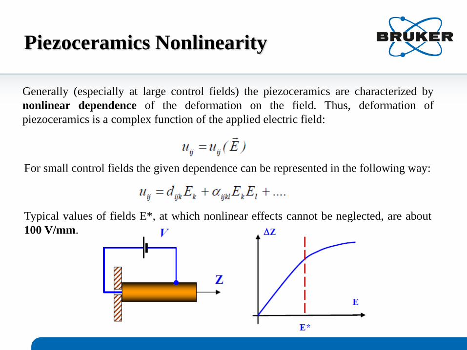
Generally (especially at large control fields) the piezoceramics are characterized by
nonlinear dependence of the deformation on the field. Thus, deformation of
piezoceramics is a complex function of the applied electric field:
For small control fields the given dependence can be represented in the following way:
Typical values of fields E*, at which nonlinear effects cannot be neglected, are about
100 V/mm.
Piezoceramics Nonlinearity

Piezoceramics creep is a delay in the response to sudden change of the control
electric field value.
The creep results in appearance of geometrical distortions in SPM images. Specifically
strong influence of the creep occurs, on initial stages of the scanning process, or after a
large displacement of the starting point of the scanned area.
Piezoceramics Creep

Piezoceramics hysteresis is that the piezoceramic deformation depends on the sign of
previously applied electric field.
To avoid distortions in the SPM images caused by piezoceramics hysteresis,
information is stored, in a sample scanning, only while tracing one of the loop
branches ΔZ = f (V ).
Piezoceramics Hysteresis

Piezoceramics Hysteresis

The sensitivity of piezoelectric materials decreases exponentially with operation time.
This causes most of the change in the sensitivity to occur at the beginning of a scanner's
life. Scanners are run approximately 48 hours before they are shipped from the factory to get
the scanner past the point where the sensitivity changes dramatically over short periods of
time. As the scanner ages, the sensitivity will change less with time, and will eventually get
to the point where it very seldom needs recalibrating.
Piezoceramics Aging
First Year- Every 3 months
Subsequent Years -Every 6 months

Acoustic waves directly affect elements of SPM heads, resulting in oscillations of the tip
with respect to the sample surface. Various protective enclosures, allowing a sensible
reduction of the level of acoustic noise are used to protect the SPM. The most effective
protection against acoustic noise is to place the measuring head into a vacuum chamber.
Protection against Acoustic Noise

AFM Probes
• An AFM probe has three components: tip, cantilever, and substrate
• There are two different shapes of cantilever: rectangular and triangular
• Key probe parameters: spring constant (k), resonance frequency (f0), and tip radius (R)
• For more information, please visit http://www.brukerafmprobes.com

Cantilever Parameters
𝑘 =𝐹
𝑍=𝐸𝑤𝑡3
4𝐿3

A wafer of silicon nitride probes for contact and fluid tapping mode imaging and
force measurement.
DNP, DNP-S, SNL, DNP-O, ScanAsyst-Air, ScanAsyst-Fluid, ScanAsyst-Fluid+
Nitride Probes

(R)TESP(A), (O)TESPA, OLTESPA, (R)FESP(A)
SCM-PIT, SCM-PIC, MESP, DDESP
Silicon Probes

1
Sample Properties
to be Measured
Topography
Viscoelasticity
Electric Properties
Magnetic Properties
2
Environment
Air
Liquid
3
Imaging Mode
Contact Mode
Tapping Topography
Tapping Phase
TRmode
Factors to Be Considered

Probe Selection Guide — Life Science

Probe Selection Guide — Material

If there is a sharp enough and unique (single valued) dependence P = P (z) of that
parameter on the tip-sample distance, then P can be used in the feedback system (FS)
that control the distance between the tip and the sample.
STMSFM
Basic Working Principle

P = P(z) Working Mode
Tunneling Current i Scanning Tunneling Microscope (STM)
Cantilever Amplitude A Tapping Mode AFM
Cantilever Deflection D Contact Mode AFM
Cantilever TR Amplitude At Torsional Resonance Mode (TRmode) AFM
Tip-Sample Force F PeakForce Tapping AFM
SPM Primary Imaging Modes

The Lennard-Jones PotentialTapping Mode
February 17, 2011 10 Bruker Confidential Information
Tapping Mode
Contact Mode
NC Mode

Simplified Block Diagram of
Contact Mode AFM
F=-kx

Tapping Cantilever in Free Air. Tapping cantilever on sample surface. Note
deflection of cantilever and return signal.
Tapping Mode AFM

Advantages and Disadvantages - Contact
Advantages
• Compared with tapping mode under same experimental conditions, the contact mode has
higher scan speeds (throughput)
• Rough samples with extreme changes in vertical topography can sometimes be scanned
more easily
• Some special applications, such as lithography, SCM, scratch, must be done under
contact mode
• Compared with tapping mode, contact mode is a “static” mode, no need to deal with
dynamics of cantilever (no tuning needed), feedback control is easier
Disadvantages
• Lateral (shear) forces can distort features in the image
• Forces normal to the tip-sample interaction can be high in air due to capillary forces
from the adsorbed fluid layer on the sample surface
• Combination of lateral forces and high normal forces can result in reduced spatial
resolution and may damage soft samples (i.e., biological samples, polymers, silicon) due
to scraping between the tip and sample

Simplified Block Diagram of
Tapping Mode AFM

Advantages and Disadvantages- Tapping
Advantages
• Compared with contact mode in air, can achieve higher lateral resolution on most
samples (1nm to 5nm)
• Compared with contact mode, tapping mode has lower forces and less damage to soft
samples imaged in air
• Lateral forces are virtually eliminated, so there is no scratching
Disadvantages
• Slightly slower scan speed than contact mode AFM
• Need to deal with dynamics of cantilever, feedback loop is harder to adjust
• Cannot be easily operated in vacuum environment
• Fluid operation is difficult
• Tip-sample interaction force is not directly controlled

Peak Force Tapping Control
Z position
Surf
ace
Time
Trajectory of the tip
approaching withdraw
1 nN
van der Waals Peak tapping force
Peak tapping force <100pN
TESP (42 N/m) on Si, MM8
800pN
-200pN
-500pN

• Automatic image optimization results in faster, more consistent results,
regardless of user skill level
• Direct force control at ultra-low forces helps protect delicate samples and tips
from damage
• Elimination of cantilever tuning, setpoint adjustment, and gain optimization
makes even fluid imaging simple
ScanAsyst Advantages

Derivation of Contact Mode
LFM
cAFM
TUNA
PFM
SCM
SSRM
SThM
Derivation of Tapping Mode
Phase Imaging
EFM
MFM
TP-KPFM
Derivation of TRmode
TR cAFM
TR TUNA
Derivation of PeakForce Tapping
ScanAsyst
PeakForce QNM
PeakForce TUNATM
PeakForce SSRM
PeakForce KPFM
Secondary Imaging Modes

The slope of the approach (loading) plot in the contact region is
related to the materials modulus (stiffness).
Softer materials will deform more under the probe resulting in
lower maximum deflection (force)
Maximum force
The minimum deflection point on the
retract (unloading) plot is the
maximum adhesion force.
The shape of the curve before
probe contacts sample can
indicate whether long range
forces (electric field, for
example) are acting on probe.
Non-Imaging Modes – Force Curve

• Surface Modification Techniques: Nanolithography, Nanoindentation,
Nanoscratching, Nanomanipulation
Surface Modification

Basic Components of SPM- Dimension Edge

Nanodrive Controller

Stage System

Dimension Stargate Head

Dimension SPM Probe Holder
Standard Non-Magnetic STM
Fluid SCM CAFM, TUNA

Lateral Resolution
Tip Shape:
The radius of curvature of the end of the tip will determine the highest lateral
resolution obtainable with a specific tip. The sidewall angles of the tip will also
determine its ability to probe high aspect ratio features.
Pixelization
Vertical Resolution
Scanner
Z Limit
Noise
Resolution Issues

Tip-Sample Convolution

The smaller the radius of curvature, the smaller the feature that can be resolved. A
sharper tip will be able to laterally resolve smaller features than a dull tip with a
larger radius of curvature. The accumulation of debris on the end of the tip can also
dull the tip and result in image distortion.
Note: A dull or dirty tip may not affect the measurement of the vertical
dimensions of these samples.
Probe Limited Resolution Dirty Probe
Tip Shape Issues

Dull or dirty tip Double or multiple tips
Typical Image Artifacts Caused by Tip

Tip Sidewall Image
Another tip artifact occurs on very tall samples or samples where the slope of the features
is greater than the slope of the tip. This causes the tip sidewall to interact with the sample
instead of the tip apex. The typical appearance is that of an almost linear ramp-like
artifact around the feature, as shown below:

Contamination from tip or sample surface
Tip/Sample Contamination
Check is there any dust or debris on the sample top surface or backside. If yes, clean it as
needed. If the sample is hydrophilic and exposed in ambient air for long time, if there is
any soft or loose residue remain on the sample after sample preparation, which can easily
contaminate the tip. If the sample is not in good condition, and hard to recover, get a fresh
clean sample.

Tapping Mode Artifacts: Not Tracking
In tapping mode, if cannot track surface, decrease the Amplitude setpoint,
decrease the scan rate or increase the I gain and P gain.
Insufficient tapping force
An excessively fast scan rate
Gain values set too low

Tapping Mode Artifacts:
High Frequency Operation
In tapping mode, decrease the Drive Frequency.

Optical Interference
Interference between the incident and reflected
light from the sample surface can produce a
sinusoidal pattern on the image with a period
typically ranging between 1.5 –2.5 μm.
It can usually be reduced or eliminated by
adjusting the laser alignment so that more light
reflects off the back of the cantilever and less
light reflects off the sample surface, or by using
a cantilever with a more reflective coating
(MESP, TESPA).

Bow
Second order bow:
the arch-shaped bow
Third order bow:
the arch-shaped bow

Technical and Application Support
Customer Care Center Support
400 Telephone Support: 400-890-5666
Team Viewer Remote Control
Email Support: [email protected]
Free Test/Repair service for warranty/service contract customers
Free Training service for warranty/service contract customers
6 big basic training classes every year (2 in Beijing, 3 in Shanghai, 1 in Guangzhou)
6 big advanced training classes every year in Beijing
Field Support
Free Field Service for warranty/service contract customers
Billable Support for out of warranty customers
Return Visit
Web Support
http://nanoscaleworld.bruker-axs.com, http://www.brukersupport.com
Training Webinars
