scanning electron microscopic investigations of peculiarities of the batio3 ferroelectric domain...
TRANSCRIPT
V. V. ARISTOV et al. : Peculiarities of BaTiO, Ferroelectric Domain Contrast 229
phys. stat. sol. (a) 78, 229 (1983)
Subjcct classification: 14.4.1; 22.8.1
Institute of Solid State Physics, Academy of Sciences of the USSR, Chernogoloakd) (a ) and Institute of Solid State Physics and Electron Vicroscopy, Academy of Sciences of the GDR, Hatle (Saale)2) (b)
Scanning Electron Microscopic Investigations of Peculiarities of the BaTiO, Ferroelectric Domain Contrast BY V. V. ARISTOV ( a ) , L. S. KOXHANCII~K (a), K.-P. MEYER (b), a n d H. BLUMTRITT (b)
Possibilities and conditions for SEM observations on barium titanate domain structures arc dis- cussed. The optimum conditions to observe domains of the samples with no conducting layer are those providing a positive charge on the surface. The samples under study are examined in the secondary electron mode at 2 to 4 kV. Under these conditions the electron microscopic contrast of the domains of different types is found to arise due to the potential effects. The mechanism of the formation of the potential contrast in BaTiO, is proposed and discussed. The charge accumu- lated on the surface at electron bombardment is considered to mainly cause the appearance of such a contrast, the latter being determined by the anisotropy of dielectric permittivity and dif- ferent conduction in various sites of the sample.
H3YYBIOTCR B 0 3 M O X H O C T M H YCJIOBHH H~6JIIO~eI1MFl AOMeHHOfi CTPYliT>’pbI THTL>HaTa 6apMH B P 3 M . OIITMManbHhIMH EJIR Ha6JIIOAeHMR HONeHOB B 06pa3qaX 6e3 IIpOBO~FiLI~~~O IIOI i~ lL lTMf l FIBJIXIOTCH yC.IIOBMflo6ecnesM~aIO~1[ae IIOJIOlfEHT~JLHYH) 3apHInIiy IIOB~pXIIOCTM. ~CCJIe~ORaHHbIe 06pa3I&I M3YqaJIMCh B peFI<HMe RTOp&I~HbIX 3JIeKTPOHOR npM 2 ZO 4 kV. B 3TMX VCJIOBHHX 3 J I ~ K T p O H H O M H I i p O C I ~ O ~ M ~ e C K H f i IiOIITpaCT AoMeHOB pa3HOrO TMna BO.3lIMKBCT 6JIarOnapR nOTeHI[HaJIbHhIM 3@@e€iTaM. AUTOIlhI B pa6oTe npeJJI2WaEOT CI 06- cyXxalOT WeXaHkI3M O ~ ~ ~ ~ O B ~ I I H R nOTeHl1llaJIhHOrO IrOHTpaCTa B BaTiO,. OCHOBHOfi n p H - YllHOfi RO3HHKHOBeHMH TaICOrO HOHTpaCTa CqHTaeTCR 3apRX, €IaliaIlJlHB~~”vI~lfi H a IIOEeIlX- IIOCTM IIpH 06JY4eHHEI 3JIelrTpoHaMH. npH 3TOM I<OHTPaCT OIIPe~eJIneTCR aHH30T~)Ollllefi ~ll3.iIeIrTpHYeCKOfi IIpOIIEIUaeMOCTH Ei pa3JIMYllOfi IIpOBO~HMOCTbIO B pa3;IH‘IHhIX nlt’CTaX o6ipaaqa.
1. Introduction
At present certain experience in visualizing ferroelectric domains in a scanning electron microscope (SEM) has been gained. The SEM enables t h e observation of some characteristic features of t he doniain structure unobservable by other techniques, e.g. by t h e optical polarization microscopy [l]. While t h e possibility of SEM obser- vations of ferroelectric domains is unanihiguous, t he na ture of the contrast, of doriiaiiis and of boundary regions between them is disputable and has been discussed only in a few publications. For instance, while t h e authors [a ] dealt only with revealing t h e topographic domain contrast of etched BaTiO, samples L e Bihan and Maussion [3] succeeded in obtaining domain structure images of non-etched and uncoated BaTiO, surfaces. They discussed this SEM potential contrast i n terms of surface charges caused by the spontaneous polarization. B u t t,he mechanism of the formation of the potential contrast of ferroelectric domains is not clear since t h e degree of compensation of t h e surface charges is unknown in most of t h e cases [4]. Furthermore, this kind
l) 142432 Chernogolovka, Moscow district, USSR. 2, Postfach 250, DDR-4020 Halle, GDR.
230 V. V. ARISTOV, L. 8. KOKHAKCH~K, K.-P. MEYEK, and H. BLUMTRITT
of domain contrast is difficult to be obtained since it can be destroyed completely by beam-induced charging of the specimen surface already after a very short time of investigation. If the surface is charged under the beam, however, a more stable contrast of the domain boundaries can occur whereas the differently polarized domain areas themselves appear with equal brightness. A satisfactory explanation of this contrast mechanism is still outstanding.
Therefore, it should be interesting to investigate the possibilities and conditions of the SEM observation of the domain structure of ferroelectrics and to study the characteristic features of the contrast under various experimental conditions. One of the most suitable ferroelectrics for such investigations is barium titanate that has a large value of the spontaneous polarization (P, = 0.26 C/m2). The domain structure of these crystals has been studied thoroughly by other techniques and is described in detail elsewhere.
The present work deals with the conditions of the SEM observations of domains and domain boundaries in BaTiO, single crystals. The observations carried out on a positively charged surface are shown to be optimum. I n this case, the peculiarities of the domain structure contrast are determined by the potential effects, but not by the surface topography. We propose and discuss a mechanism of the potential contrast formation due to the surface charge under electron bombardment and deter- mined by the anisotropy of the dielectric permittivity and by the inhomogeneity of the conductivity.
2. Experimental Results
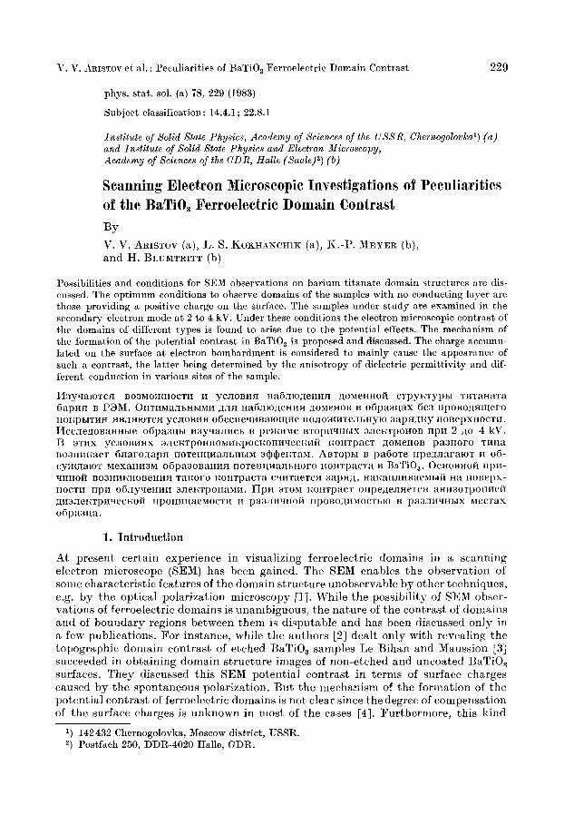
I n order to investigate the conditions of the doiiiain structure contrast formation we used thin (200 pm) barium titanate crystals with (001) surface orientation. The crystals contained various domain types. Fig. 1 presents the micrograph of a typical crystal region obtained in a polarization optical microscope. Laminar groups of a-domains are seen to intersect the large c-domain (the dark region in the centre of Fig. 1) in two mutually perpendicular directions. At places of intersection one can see stripes in the (110) directions being a-a doinain boundaries (see, for instance, [ 5 ] ) .
Since a-domains intersect the crystal a t an angle of 45" with respect to the (001) sur- face, in the optical image we see their pro- jection onto the (001) plane. Accordingly, because of the superposition of the upper and lower domain parts the number of the observed lines may not be coincident with the actual number of the domains. Apart from that, no information on the c-c-do- main configurations can be obtained from the optical image.
Fig. 1. Image of the ferroelectric domains in a BaTiO, crystal obtained in a polarization optical microscope
Peculiarities of the BaTiO, Ferroelectric Domain Contrast 231
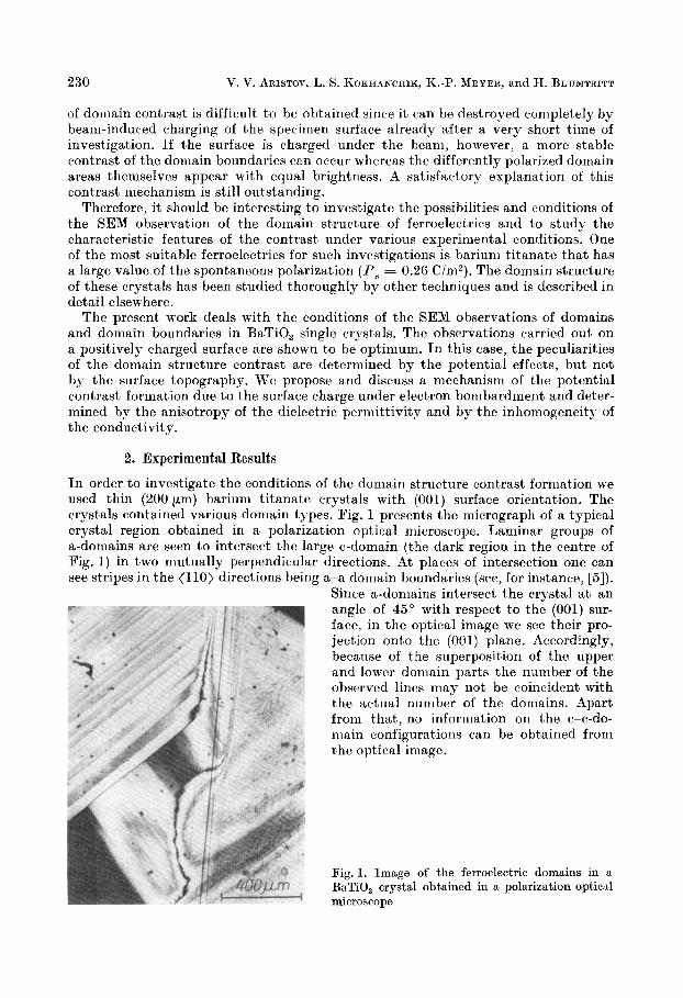
Fig. 2. SEM image of the same crystal region as in Fig. 1 ob- tained in the secondary emis- sion mode a t an accelerating voltage of 2 kV
The SEM observations were carried out in a JSM 35-C microscope in the secondary emission mode at low accelerating voltages. In a particularly small range of accelerat ing voltages one can select the conditions for every dielectric when the effect of the beam-induced surface charging is insignificant, i.e. when the electron emission coeffi- cient 4 = 7 + 6 is close to unity (q is the coefficient of back-scattering, 6 the coeffi- cient of the secondary electron emission) [6]. There are some papers which describe the domain structure of ferroelectrics observed under these conditions [3, 71. The equilibrium accelerating voltage U, at which A = 1 has to be selected experimentally, for our BaTiO, it was between 3 and 4 kV.3) We failed, however, to obtain a good contrast under strict equilibrium conditions. The domain structure yielded a clear image, usually, with a positive charge prevalent on the surface. Fig. 2a presents an SEM iiiiage of the above-described domain configuration of the same sample obtained a t an accelerating voltage of 2 kV. In Fig. 2 b at a higher magnification laminar a-domains are seen to have a wedge-shaped configuration with the wide part being
’) The voltage in a JSM 35-C microscope is varied in a stepwise manner, the step being 1 kV. The condition d = 1 can be obtained a t U,, 2 U,, by tilting the sample with respect to the elec- tron beam. With increasing angle of incidence the coefficient 6 also increases.
232 V. V. ARI~TOY, L. S. KOKHANCHIK, K.-P. MEYER, and H. BLUNTRITT
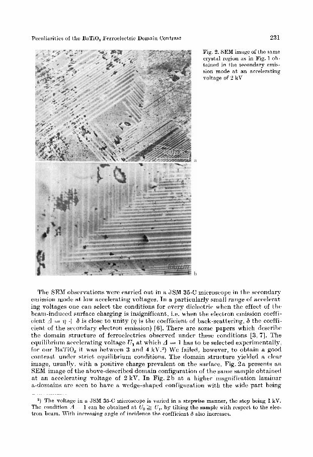
Fig. 3. a) c-c niid b) a-c do. main configurations, 2 kV
less than 10 p i . These wedge-shaped domains are known to be niost niohile, and decrease or increase in size under the effect of external factors. IZ'e have observed these changes in the saiiiple in a repeated observation (Fig. 2a, h). The identical
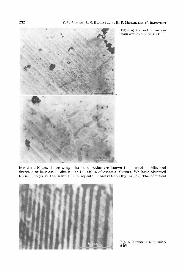
Fig. 4. K\'arrow a-c domains, 2 kV
Peculiarities of the RaTiO, B'erroelectric Domain Contrast 233
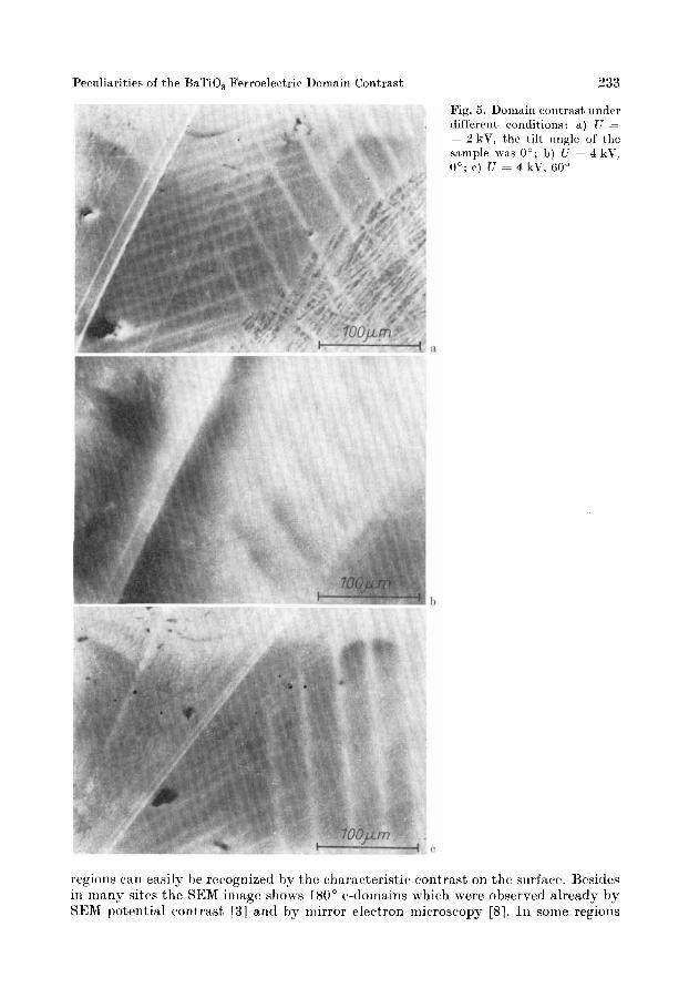
Fig. 5. Domain contrast under different conditions: a ) 7: 2 = 2 kV, the tilt angle of the sample was 0"; b) U = 4 kV, 0"; C ) U = 4 kV, 60"
regions can easily be recognized by the characteristic contrast on the surface. Besides in niany sites the SEM image shows 180" c-domains which were observed already by SEM potential contrast [3] and hy niirror electron inicroscopy [8]. I n some regions
234 V. V. ARISTOV, L. S. KOKHANCHIK, K.-P. MEYER, and H. BLUMTRITT
we observed not only the light boundary contrast between these c-domains but, also, a darker contrast of the domains of reversed sign (Fig. 3). Despite of the low accel- erating voltages a t which we carried out our investigations we managed to obtain an SEM image of very narrow a-c domains (Fig. 4). I n some regions the domain thickness did not exceed 1 p i .
The SEM contrast observed a t a particular positive charge of the surface can be divided into the contrast of domains and that of boundary regions. Most stable in time and bright in tone with regard to its surroundings is the contrast of domain boundaries. By changing the accelerating voltage of the beam to values U > U,, the sample surface begins to get negatively charged because the value of A becomes less than unity. Under these conditions the contrast of a-c domain boundaries is reversed, 1.e. the bright regions of a-donlain boundaries become darker. The general conditions of visibility a t negative charge are much worse than those a t positive charge. Close to the point corresponding to U,. one can obtain different contrasts by simply tilting the sample with respect to the primary beam, i.e. by altering the coefficient of the secondary electron emission. Fig. 5a, b, c present the image of the domains belonging to the same region under different observation conditions. In several cases close to the equilibrium point different domain contrasts were observed with the beam scan- ning rate considerably changing. Similar changes in contrast of the boundary regions between 18O0-domains were observed in TGS crystals, too [7, 91.
The dependence of the contrast of a-c domains in barium titanate on the sur- face charge conditions confirms its potential nature. This is also supported because at such low accelerating voltages one cannot observe the topography of surface steps at the a-c boundaries caused by the weak tetragonality of BaTiO,.
3. Discussion
Up to now a satisfactory explanation of the contrast of domains and boundaries in the SEM seems to be missing. According to Le Bihan et al.'s suggestion one should expect the best domain contrast a t the equilibrium accelerating voltage. I n this case the surface potentials caused by the spontaneous polarization make the domains appear as bright and dark areas since the surface charges are not always fully compensated [lo]. Only few examples of such a contrast which tends to vanish during the imaging process can be found in the literature, however, see e.g. [ll, 121.
On the other hand, the contrast of domain boundaries is rather stable especially if the surface is charged positively a t low accelerating voltages. When passing the equilibrium and using higher voltages the boundary contrast reverses. This was found not only for TGS but also for GASH [13] and GMO [14].
As described, our BaTiO, specimens exhibited the same behaviour of the boundary contrast, whereas the contrast practically vanished in the vicinity of the equilibrium voltage. For this reason we attempt to explain the observed contrast in terms of the beam-induced charging depending on different values of permittivity and resistivity a t different points of the sample.
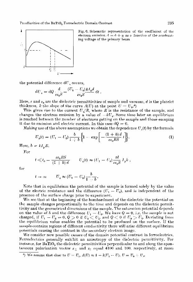
Jn order to find the parameters which determine such an induced potential contrast we shall analyse the process of the charging of a homogeneous plane-parallel dielectric sample in the scanning electron microscope. Fig. 6 gives a schematic graphic represen- tation of the dependence A ( U ) . For an equilibrium value U = U, the coefficient of the electron emission A equals unity. A displacement of the accelerating voltage from the equilibrium position by a value of AU = brl - LTo causes the appearance of the surface charge dQ equal to ( A - 1) Ip dt, where dt is the irradiation time, Ip the electron current. Accordingly, between the two surfaces of the dielectric of the area S
Pcoitliaritics of the BsTiO, Fcrroelectric Domain Contrast 235
Fig. 6 . Schematic representation of the coefficient of the electron emission d = b + q as a function of the accelerat-
the potential difference dCs occurs,
Here, E and E , are the dielectric permittivities of sample and vacuum, d is the platelet thickness, k the slope of the curve A ( U ) a t the point U = U0.4)
This gives rise t o the current U,/R7 where R is the resistance of t,he sample, and changes the electron emission by a value of --kU,. Some time later an equilibriuni is reached between the number of electrons getting on the sample and those escaping it due to emission and electric current. I n this case dQ = 0.
Making use of the above assumptions we obtain the dependence U,( t ) by the formula
Here, b = kIpl? . For
for
t + o o U s NN ( U , - b L70) ~fb.
Note that in equilibrium the potential of the sample is formed solely by the value of the electric resistance and the difference ( U , - Uo)7 and is independent of the presence of the surface charge prior to experiment.
We see that a t the beginning of the bonibardment of the dielectric the potential on the sample changes proportionally to the time and depends on the dielectric perniit- tivity and the geometrical diniensions of the sample. The saturation potential depends on the value of b and the difference U, - U,. We have Q = 0, i.e. the sample is not charged, if U, - U, = 0, Q > 0 if U , < U,, and Q < 0 if U, > V,. Deviating froin the equilibrium value enables the potential to be produced on the surface. If the sample contains regions of different conductivity there will arise different equilibriun: potentials causing the contrast in the secondary electron image.
We consider now possible causes of the domain potential contrast in ferroelectrics. Ferroelectrics generally exhibit an anisotropy of the dielectric permittivity. For instance, for BaTiO, the dielectric permittivities perpendicular to and along the spon- taneous polarization vector EL and E , , equal 4100 and 160, respectively, at room
4, We assume that close to U = U,, d ( U ) z 1 + k(C, - U ) , U = U,, + U,.
236 V. V. ARISTOV e t al.: Peculiarities of BaTiO, Ferroelectric Domain Contrast
temperature [4]. Formula (1) suggests that the great difference in E for a- and c-domains can be one reason for the good contrast observed under the particular experimental conditions. It has been pointed out above that the contrast of the domain boundary regions is most stable, its sign being reversed with the reversal of the surface charge sign. These regions are always charged less than the domains. The SEN1 images of the boundaries should be noted to be up to 1 pni wide. The boundary regions are likely bo have a considerably greater conductivity than the other regions of ferroelectrics. Probably, due to the strong electric fields in the boundary regions impurities are accu- niiilated there which increase the conduction.
Thus, we have shown that the contrast of BaTiO, ferroelectric doinains can be qualitatively explained as being due to the potential which is produced by the electron beam bombardment of the sample a t U,, + bTl and may vary due to differen- ces in the dielectric perniittivity and the conductivity a t different points of the sample. We conclude that the proposed model of an electron beam-induced potential contrast of ferroelectric speciinens is an additional possible explanation of the observed electric donlain contrast in the SEM. This is valid in so far as the anisotropy of permittivity and resistivity corresponds to the domain structure. It does not exclude, of course, that under appropriate equilibrium conditions the inherent surface potential distri- bution of the specimen can give rise to a donlain structure image.
References
[11 L. A. SHC'V%LO\, 1'. A. KIRIMOV, K. S. C ~ O S D O V E R , I. S . ZHELVUEV, md V. T. PETROI, phys.
121 G. I*. ROBIhsON and It. b1. KHITE, Appl. Phys. Letters 10, 320 (1967). [3] K. LE B I H A ~ and 31. M A I J ~ ~ ~ O X , C. R. Acad. Sri. (Franrc) 5 4 , 1073 (1972); Frrroelectiics i ,
141 11. E. LIhiE5 and A. 31. G L I ~ I , Principles and Apphrationy of Ferroelectricr and Kclated
[,5] P. JV. FORSBERCH, JR., Phys. Rev. i 6 , 1187 (1949). [O] J. I. GOLDSTEIX and H. YIKOWITZ (Ed.), Practical Scanning Electron Jlicroicopy, Plrnum
[ 7 ] R. LE BIHIX and M. hlausi~oh-, J. Physique 33, C2-21.i (1972). 181 F. I,. E~CLISH, J. appl. Phys. 3!), 3231 (1968). [9] D. G. COATIX and K. Siriw, I'roc. 7th Internat. Congr. Electron Microscopy, Vol 1 , Grenoble
101 R. LE BIHIN, J. 1,. CHinTiaR, and L. JEIX, Ferroelectrics 13, 475 (1976). 111 R. LE B I H ~ N and 31. NILS~IOY, C.R. A ~ a d . Sci. (France) "2, 1010 (1971). 121 S. T K E D L and Y. UCHIKIWI, J . Electron Microscopy 29, 209 (1980). 131 K. La BIHAN and G . JOLET, Fcrroelertrics 26, 843 (1980). 141 K.-P. TtTci m, H RLTTIITRITT, and 1,. SZ~ZE~NIAK, Ultr~imirroscopy f i , 67 (1981).
stat. sol. (a ) 28, 677 (1975).
307 (1974).
JIateri,ils, Cl'trendon Press, Oxford 1977.
Press, New Pork/London 1975.
1970 (p. 259).
( R e w i i pi1 10. 1483)