scaled planar floating-gate nand flash memory technology: challenges...
TRANSCRIPT

SCALED PLANAR FLOATING-GATE NAND FLASH MEMORY
TECHNOLOGY: CHALLENGES AND NOVEL SOLUTIONS
A DISSERTATION
SUBMITTED TO THE DEPARTMENT OF ELECTRICAL ENGINEERING
AND THE COMMITTEE ON GRADUATE STUDIES
OF STANFORD UNIVERSITY
IN PARTIAL FULFILLMENT OF THE REQUIREMENTS
FOR THE DEGREE OF
DOCTOR OF PHILOSOPHY
Shyam Raghunathan
October 2010
http://creativecommons.org/licenses/by-nc/3.0/us/
This dissertation is online at: http://purl.stanford.edu/yy374yj9591
© 2011 by Shyam Sunder Raghunathan. All Rights Reserved.
Re-distributed by Stanford University under license with the author.
This work is licensed under a Creative Commons Attribution-Noncommercial 3.0 United States License.
ii

I certify that I have read this dissertation and that, in my opinion, it is fully adequatein scope and quality as a dissertation for the degree of Doctor of Philosophy.
Krishna Saraswat, Primary Adviser
I certify that I have read this dissertation and that, in my opinion, it is fully adequatein scope and quality as a dissertation for the degree of Doctor of Philosophy.
Yoshio Nishi, Co-Adviser
I certify that I have read this dissertation and that, in my opinion, it is fully adequatein scope and quality as a dissertation for the degree of Doctor of Philosophy.
Tejas Krishnamohan
Approved for the Stanford University Committee on Graduate Studies.
Patricia J. Gumport, Vice Provost Graduate Education
This signature page was generated electronically upon submission of this dissertation in electronic format. An original signed hard copy of the signature page is on file inUniversity Archives.
iii

- iv -
This page is intentionally left blank

Abstract
- v -
Abstract
Flash memory is the most widely used non-volatile information-storage device
today. NAND flash memories are ubiquitous in their use as portable storage media in
cellphones, cameras, music players, and other portable electronic devices. In addition,
NAND flash memory has recently seen rapid adoption as solid-state drives (SSD) in
place of hard-disk drives (HDD) in modern personal computers and data servers. In
addition to greater speed and better endurance against mechanical damage, SSDs also
consume much lesser power than HDDs.
The NAND flash memory device, consisting of a floating-gate transistor cell,
is the most aggressively scaled electronic device, as evidenced by ever-increasing
memory capacities. In this work, we will examine possible problems arising from
continued scaling of these structures, and discuss novel solutions to overcome them.
Firstly, we investigate scaling of the conventional poly-silicon floating-gate,
aimed at reducing cell-to-cell interference. We experimentally delineate a new
reliability concern for the first time, with programming current through ultra-thin

Abstract
- vi -
poly-silicon floating-gates becoming increasingly ballistic. We also experimentally
demonstrate doping-related issues in the poly-silicon floating-gate.
We then apply a novel metal-based floating-gate cell for the first time,
designed to overcome the problems discussed above. We explore factors that influence
the choice of metal, and demonstrate excellent functionality in ultra-thin metal
floating-gate cells scaled down to 3 nm TiN floating-gate thickness, thus greatly
reducing cell-to-cell interference.
Finally, in order to facilitate continued scaling of the control dielectric, we
explore replacement of the conventional silicon oxide-nitride dielectric with high-k
dielectric materials. We integrate poly-silicon floating-gate cells with Al2O3 high-k
control dielectric, and show that the presence of a silicon nitride inter-layer improves
the interface between the floating-gate and the control dielectric. We also integrate
metal floating-gate cells with Al2O3 control dielectric, and these cells exhibit very
good electrical characteristics. Further, we establish that a deeper work-function
control gate is helpful in reducing gate-injection.
Combining ultra-thin metal floating-gate, high-k control dielectric and deep
work-function control gate, we enable the planar floating-gate cell as a scalable
candidate.

Acknowledgements
- vii -
Acknowledgements
This work would not have been possible without the help and guidance of
many individuals. First and foremost, I would like to express my deepest gratitude to
my advisor, Prof. Krishna Saraswat. Right from the day that I arrived at Stanford, his
constant support and guidance has been invaluable to my progress. He is undoubtedly
one of the kindest people I have ever met, and his calm and cheerful demeanor is very
inspiring. I would like to specially thank him for his support when I wanted to change
my topic of work. His support in encouraging his students to explore a range of topics,
is critical to the successful and enjoyable experience that his students have. I have
been very fortunate to have had the best advisor anyone could hope for, and it has
been an honor to be part of his illustrious research group.
I would like to express my sincere gratitude to my co-advisor, Prof. Yoshio
Nishi. I have received many valuable suggestions and feedback from him during the
course of my time at Stanford. I am very grateful to have been acquainted with him.
I am indebted to Prof. Tejas Krishnamohan for his guidance and support all
through my time here. Even as a student in the group, he was an inspiration to me. He
is truly one of the smartest people I have ever interacted with, and his guidance has

Acknowledgements
- viii -
been extremely critical to my progress. I am especially thankful for the long
discussions that we often had late in the night, in spite of his incredibly busy schedule.
I am extremely fortunate to have had the opportunity to be mentored by him.
I would like to thank Prof. Pierre Khuri-Yakub for agreeing to chair my orals. I
am very grateful to Dr. Ann Marshall for her help with TEM imaging. I would like to
express my gratitude to Dr. Jim McVittie and Dr. Eric Peroziello for all their help in
the lab. I am very thankful to Prof.Ted Kamins for the many useful discussions and
feedback.
All my experimental work was performed at the Stanford Nanofabrication
Facility. I would like to thank the staff for enabling a world-class research facility.
I am very grateful to Dr. Pranav Kalavade, Dr. Krishna Parat, Dr. Kiran
Pangal, Dr. Prashant Damle and Dr. Sanjay Rangan for their guidance and support
during my internship at Intel.
I have been fortunate to have had the support of amazing friends and
colleagues over the last few years at Stanford : Abhijit, Albert, Ali, Ammar, Aneesh,
Anshul, Arunanshu, Arvind, Bob, Caner, ChiOn, Crystal, David, Debbie, Donguk,
Donghyun, Donkoun, Duygu, Ed, Elmer, Emel, EricP, Eunji, Filip, Gail, Gaurav,
Girish, Gunhan, Hai, Hemanth, Hiro, Hoon, Hoyoel, Hyun-Yong, Irene, J, Jae, Jason,
Jeannie, Jenny, Jia, Jim, Jin-hong, John, Jungyup, Kavya, Kiran, Kishore, Krishna,
Kyeongran, Kyung-hoae, Lan, Mahnaz, Manar, Manoj, Marika, Mary, Masaharu,
Masato, Maurice, Mihir, Munehiro, Nancy, Nevran, Nishant, Onur, Paul, Pawan,
Peter, Pranav, Prasanthi, Prashant, Raghav, Raja, Rajesh, Ray, Rishi, Robin, Rohit,
Rostam, Roozbeh, Sangbum, Sanjay, Sarves, Shankar, Serene, Shreekar, Simon,
Acknowledgements
- ix -
Suman, Sumanth, Suyog, Swaroop, Szu-lin, Shen, Ted, Uli, Wooshik, Yasuhiro, Yeul,
Yuan, Yuniarto, Ze.
No words would ever do justice to express my deepest thanks and gratitude to
my most wonderful family – my parents and my sister. Their unconditional love,
sacrifice, support and encouragement have allowed me to pursue my ambitions.

Acknowledgements
- x -
This page is intentionally left blank

Table of Contents
- xi -
Table of Contents
Abstract .............................................................................................................................. v
Acknowledgements .......................................................................................................... vii
Table of Contents .............................................................................................................. xi
List of Tables ................................................................................................................... xiv
List of Figures .................................................................................................................. xv
Chapter 1 – Introduction .................................................................................................. 1
1.1 Motivation ......................................................................................................... 1
1.2 Thesis Organization ........................................................................................... 5
References ..................................................................................................................... 8
Chapter 2 – Flash Memory: Operation and Scaling ...................................................... 9
2.1 Introduction ....................................................................................................... 9
2.2 What is Flash Memory? ..................................................................................... 9
2.3 The Floating-gate Cell ..................................................................................... 12
2.3.1 Gate coupling ratio (GCR) ........................................................................ 15
2.4 Read Operation ................................................................................................ 16
2.5 Multi-level Cell (MLC) ................................................................................... 17
2.6 Types of Flash Memory ................................................................................... 18
2.7 Mechanisms of Charge Injection ..................................................................... 21
2.7.1 Channel hot electron (CHE) injection ....................................................... 21
2.7.2 Fowler-Nordheim tunneling ...................................................................... 23

Table of Contents
- xii -
2.8 Reliability of Flash Memories ......................................................................... 27
2.8.1 Endurance (Cycling) .................................................................................. 27
2.8.2 Retention .................................................................................................... 28
2.9 Flash Memory Scaling ..................................................................................... 30
2.9.1 Challenges in scaling NOR flash ............................................................... 31
2.9.2 Challenges in scaling NAND flash ............................................................ 33
References ................................................................................................................... 37
Chapter 3 – Scaled Poly-Silicon Floating-Gate NAND Flash Memory ...................... 41
3.1 Introduction ..................................................................................................... 41
3.2 Motivation ....................................................................................................... 42
3.2.1 Cell-to-cell interference ............................................................................. 42
3.2.2 Control gate wrap-around .......................................................................... 45
3.3 Floating-gate thickness scaling ........................................................................ 49
3.4 Experimental Test Structure ............................................................................ 50
3.5 Fabrication ....................................................................................................... 52
3.6 Measurement Setup ......................................................................................... 55
3.7 Program/Erase characteristics ......................................................................... 56
3.8 Retention .......................................................................................................... 62
References ................................................................................................................... 64
Chapter 4 – Scaled Poly-Silicon Floating-Gate: Problems to Ultimate Limit ........... 67
4.1 Introduction ..................................................................................................... 67
4.2 The Ballistic Problem ...................................................................................... 68
4.2.1 Ballistic transport ....................................................................................... 68
4.2.2 Ballistic transport during programming .................................................... 69
4.2.3 Test Structure ............................................................................................. 71
4.2.4 Measurement ............................................................................................. 73
4.2.5 Results ....................................................................................................... 77
4.2.6 Verification ................................................................................................ 81
4.2.7 Mean Free Path .......................................................................................... 84
4.2.8 Impact (Endurance) ................................................................................... 85
4.2.9 Summary .................................................................................................... 89

Table of Contents
- xiii -
4.3 Poly-silicon depletion ...................................................................................... 89
4.3.1 Poly depletion effect .................................................................................. 89
4.3.2 Poly depletion in NAND flash memory .................................................... 91
4.3.3 Experiment ................................................................................................ 93
4.3.4 Summary .................................................................................................... 98
References ................................................................................................................... 99
Chapter 5 – Metal Floating-Gate ................................................................................. 101
5.1 Introduction ................................................................................................... 101
5.2 Metal Floating-Gate Device .......................................................................... 102
5.3 Ballistic Component in Metal Floating-Gates ............................................... 105
5.4 Absence of Poly-depletion effects ................................................................. 110
5.5 Metal floating-gate work-function ................................................................ 112
5.6 Choice of metal : TiN, TaN ........................................................................... 115
5.7 Ultra-thin 3 nm TiN floating-gate device ...................................................... 116
5.8 Summary ........................................................................................................ 118
References ................................................................................................................. 119
Chapter 6 – High-k dielectric IPD ............................................................................... 121
6.1 Introduction ................................................................................................... 121
6.2 Motivation ..................................................................................................... 122
6.3 Choice of high-k dielectric for IPD application ............................................ 125
6.4 Poly-silicon FG with Al2O3 IPD .................................................................... 128
6.5 Metal floating-gate device with Al2O3 IPD ................................................... 135
6.6 Control-Gate .................................................................................................. 139
6.7 Summary ........................................................................................................ 139
References ................................................................................................................. 142
Chapter 7 – Conclusions and Future Directions ........................................................ 145
7.1 The Planar Floating-Gate Device .................................................................. 145
7.2 Future Directions ........................................................................................... 148

List of Tables
- xiv -
List of Tables
Table 2.1: Major differences between NOR and NAND flash memories
Table 5.1: Work-functions and Fermi energies of some elements [5.11, 5.12]
Table 6.1: Common high-k dielectrics [6.14]

List of Figures
- xv -
List of Figures
Figure 1.1 Applications of flash memory ....................................................................... 1
Figure 1.2: Demand for NAND flash memory (Source: Gartner May 2009,
Semiconductor Forecast Database (SEQS-WW-DB) [1.2]) .......................................... 2
Figure 1.3: Comparison of SSD and HDD (Source: Micron) ........................................ 3
Figure 1.4: World-wide data center power savings with SSD compared to HDD.
(Source: Samsung) .......................................................................................................... 3
Figure 1.5: Scaling of NAND flash memory. The pace is 2X per year as opposed to
2X every 1.5 years according to Moore‟s Law. (Source: Samsung) .............................. 4
Figure 2.1 : Non-volatile MOS memory qualitative comparison in the flexibility-cost
plane (From [2.1]) ........................................................................................................ 10
Figure 2.2: Semiconductor memory market for flash, DRAM and SRAM (Source:
[2.1], [2.10]) ................................................................................................................. 11
Figure 2.3: Cross-section schematic of a floating-gate transistor ................................ 12
Figure 2.4: Band diagrams for the neutral state (left) and charged state (right) of the
floating-gate transistor. (Source: [2.1]) ........................................................................ 13

List of Figures
- xvi -
Figure 2.5: Schematic showing the capacitive coupling of the floating-gate (Source
[2.12]) ........................................................................................................................... 14
Figure 2.6: I–V curves of an FG device when there is no charge stored in the FG
(curve A) and when a negative charge Q is stored in the FG (curve B) [2.12, 2.15]. .. 17
Figure 2.7 : Two different threshold voltage states lead to 1 bit per cell storage while
four different threshold voltage states lead to 2 bits per cell. ....................................... 18
Figure 2.8 : NOR and NAND flash arrays with layout comparison (Source: Intel
[2.11]) ........................................................................................................................... 19
Figure 2.9 : NOR flash programming using CHE injection [Source: Intel] ................. 22
Figure 2.10 : A schematic energy band diagram describing the three processes
involved in electron injection [2.22] ............................................................................ 23
Figure 2.11 : F-N tunneling of electrons from the poly-Si FG into the Si substrate
through the triangular energy barrier posed by the tunox. (Source: [2.12]) ................. 24
Figure 2.12 : F-N tunneling current as a function of electric field (Source: [2.12],
[2.27]) ........................................................................................................................... 25
Figure 2.13: F-N programming in NAND flash (Source [2.11]) ................................. 26
Figure 2.14 : Threshold voltage window closure caused by traps in the tunnel oxide as
a function of program/erase cycles on a single cell, showing endurance characteristics
[2.1]. ............................................................................................................................. 28
Figure 2.15: Band diagram showing charge-retention state and leakage path through
dielectrics ...................................................................................................................... 29
Figure 2.16 : NOR flash memory scaling (Source: Intel [2.11]) .................................. 30
Figure 2.17 : NAND flash Bit Density Scaling Trend (Source: [2.34]) ....................... 31
List of Figures
- xvii -
Figure 2.18: NOR flash ITRS Scaling Projection [2.36] .............................................. 33
Figure 2.19 : ITRS Scaling projections for floating-gate NAND flash. [2.36] ............ 36
Figure 3.2 : Floating-gate interference causes undesirable shift in threshold voltage of
one cell due to adjacent cells (Source: [3.7]) ............................................................... 43
Figure 3.3: This figure depicts the shifting of threshold voltage of Cell 1 when Cell 2
gets programmed due to the parasitic coupling between the adjacent cells. (Source:
[3.6]) ............................................................................................................................. 44
Figure 3.4: The undesirable threshold voltage shift (interference) is getting worse with
scaling. (Source: [3.8], [3.9]) ........................................................................................ 44
Figure 3.5: Control-gate is wrapped around the FG shielding interference between
adjacent floating-gates .................................................................................................. 46
Figure 3.6: Image showing CG wrapping around the FG [3.10] .................................. 46
Figure 3.7: Changing the height of the CG wrap-around has a significant effect on the
word-line direction interference [3.10] ......................................................................... 47
Figure 3.8 : Interference along BL direction and WL direction [3.11] ........................ 47
Figure 3.9: CG no longer has space to wrap around FG thereby leading to a serious
interference problem and GCR decrease. ..................................................................... 48
Figure 3.10 : Image showing that the distance between cells is extremely less (Source:
[3.13]) ........................................................................................................................... 48
Figure 3.11: Reduction of FG height greatly reduces FG interference. ....................... 49
Figure 3.12: Shows that for future nodes, required FG height is a few nm. (Source:
[3.16]) ........................................................................................................................... 50
Figure 3.13: Schematic of experimental test structure ................................................. 51

List of Figures
- xviii -
Figure 3.14: TEM image of the gate with ultra-thin 7 nm poly-silicon floating-gate. A
very smooth layer is obtained at such a low thickness. ................................................ 54
Figure 3.15: TEM image showing ultra-thin 7 nm poly-silicon floating-gate ............. 55
Figure 3.16: Programming characteristics of 75 nm thick n-type poly-silicon floating-
gate ............................................................................................................................... 57
Figure 3.17 : Erasing characteristics of 75 nm n-type poly-silicon floating-gate ........ 58
Figure 3.18: Programming characteristics for various thicknesses of n-type poly-
silicon FG devices ........................................................................................................ 61
Figure 3.19: Erasing characteristics for various thicknesses of n-type poly-silicon FG
devices .......................................................................................................................... 61
Figure 3.20: Retention for n-type poly-Si FG devices of various thicknesses ............. 62
Figure 4.1 : Schematic band diagram of ballistic transport and emission via multiple
tunneling through interconnected nanocrystallites in porous silicon under a high
electric field. [4.7] ........................................................................................................ 69
Figure 4.2: Band diagram describing ballistic transport during programming. ........... 70
Figure 4.3 : Test Structure used to study ballistic transport ......................................... 71
Figure 4.4: Band diagram during measurement at low FG bias. Substrate is grounded
and CG is fixed at 20 V. ............................................................................................... 74
Figure 4.5: Shows the IPD leakage current at the start of measurement. ..................... 74
Figure 4.6: Band diagram of measurement at high FG bias. ........................................ 75
Figure 4.7: Shows schematics of expected currents at mid-to-high floating-gate bias.75
Figure 4.8: Schematic of expected currents during the ballistic current measurement
technique described. ..................................................................................................... 77

List of Figures
- xix -
Figure 4.9: Ballistic measurement data: 75 nm n-type poly-silicon floating-gate ....... 78
Figure 4.10: Ballistic component measurement data in 30 nm n+ poly-silicon floating-
gate device .................................................................................................................... 79
Figure 4.11: Ballistic component measurement data for 10 nm n+ poly-silicon
floating-gate sample ..................................................................................................... 80
Figure 4.12 : Shows two floating-gate structures with the same IPD area (region
between FG and CG) but different active areas (tunnel oxide region) ......................... 82
Figure 4.13: Ballistic component measurement data on 11 nm poly-silicon floating-
gate sample for structures with different active areas. ................................................. 83
Figure 4.14: Magnified version of figure 4.13 ............................................................. 83
Figure 4.15: Inelastic mean free path extraction by slope of ballistic component versus
floating-gate thickness .................................................................................................. 85
Figure 4.16: Cycling data (+- 14 V, 100 ms) on 75 nm, 10 nm and 7 nm poly-silicon
floating-gate devices. The 7 nm floating-gate devices show more degradation .......... 86
Figure 4.17: Cycling data (+17 V, 100 µs and -14 V, 100 ms) on 75 nm and 10 nm
poly-silicon floating-gate devices. The 10 nm floating-gate devices show more
degradation ................................................................................................................... 87
Figure 4.18: Capacitance-Voltage curves of cycled devices indicating more
degradation in the 10 nm poly-silicon floating-gate device compared to the 75 nm
floating-gate device. ..................................................................................................... 88
Figure 4.19: The poly-depletion effect. Due to the depletion in the poly-silicon gate,
the effective oxide thickness increases and the effective capacitance decreases. Source:
[4.13] ............................................................................................................................ 90

List of Figures
- xx -
Figure 4.21: As a result of the poly-depletion, there is a decreased field across the
tunnel oxide which makes the erase slower. Source: [4.15] ......................................... 92
Figure 4.22: Shows the capacitance-voltage plots for poly-silicon floating-gate
devices. The 7 nm device shows a characteristic poly-depletion dip in the capacitance.
...................................................................................................................................... 93
Figure 4.23: The poly-depletion effect is much more pronounced for larger emulated
wraps ............................................................................................................................. 95
Figure 4.24: Medici simulation potential contours for depleted and undepleted FG.
Shows effect of emulated wrap in amplifying poly-depletion. .................................... 96
Figure 4.25: Shows slower programming in 7 nm poly-silicon floating-gate device due
to poly-depletion. .......................................................................................................... 97
Figure 5.1: Floating-gate capacitor structure used to study program/erase and
reliability performance of metal floating-gate devices. .............................................. 102
Figure 5.2: TEM of a metal (TiPt) floating-gate device gate-stack ........................... 103
Figure 5.3: Programming characteristics of TiPt floating-gate device ....................... 104
Figure 5.4: Erasing characteristics of TiPt floating-gate device ................................ 104
Figure 5.5: Structure with floating-gate contact used to measure the ballistic
component of tunnel oxide current. ............................................................................ 106
Figure 5.6: Ballistic component measurement data on 7 nm TiPt metal floating-gate
sample. The metal has much lower ballistic component compared to poly-silicon of
the same thickness. ..................................................................................................... 106

List of Figures
- xxi -
Figure 5.7: Percentage of ballistic current plotted versus floating-gate thickness for a
variety of materials. In general, it can be observed that metals have lower ballistic
component compared to poly-silicon due to increased inelastic electron scattering. . 107
Figure 5.8: Shows the definition of work-function and Fermi energy in a metal. Also
shows the density of states (DOS) versus energy. ...................................................... 108
Figure 5.9: Capacitance-Voltage plot of 3 nm TiN FG capacitor showing no
characteristic poly-depletion dip in the capacitance. .................................................. 111
Figure 5.10: Flat-band voltage versus programming time for 3 nm TiN FG sample.
There is no slow-down in the beginning as observed with depleted poly-silicon
samples due to decreased GCR. ................................................................................. 111
Figure 5.11: Band diagrams showing that deeper work-function FG leads to slower
erase. Top figure shows shallower work-function FG device and bottom figure shows
deeper work-function FG device. Deeper work-function FG has larger barrier to
tunneling out from FG to substrate. ............................................................................ 113
Figure 5.12: Band diagrams showing that deeper work-function FG leads to better
retention. Top figure shows shallower work-function FG device and bottom figure
shows deeper work-function FG device. Deeper work-function FG device stores
charge in a deeper potential well. ............................................................................... 114
Figure 5.13: Shows deeper work-function (Pt) FG device erase slower than shallower
work-function (Ti+Pt) FG device ............................................................................... 115
Figure 5.14: Programming characteristics of 3 nm TiN FG device showing excellent
performance ................................................................................................................ 117

List of Figures
- xxii -
Figure 5.15: Erasing characteristics of 3 nm TiN FG device showing excellent
performance ................................................................................................................ 117
Figure 5.16: Retention data for 3 nm TiN floating-gate device ................................. 118
Figure 6.1: Image of control-gate wrapping around floating-gates [6.11] ................. 123
Figure 6.2: CG no longer has space to wrap around FG thereby leading to a serious
interference problem and GCR decrease .................................................................... 123
Figure 6.3: Image shows that the distance between cells is very less (Source: [6.12])
.................................................................................................................................... 124
Figure 6.4: Shows erase-saturation occurring as a result of gate-injection. A larger
conduction barrier height of the IPD would reduce injection from the control-gate. 126
Figure 6.5: Common high-k dielectrics. In general, larger the dielectric constant,
smaller the band-gap. [6.14] ....................................................................................... 127
Figure 6.6: TEM image of the gate-stack of a poly-silicon FG Al2O3 high-k IPD
device .......................................................................................................................... 128
Figure 6.7: Program characteristics of 60 nm poly-silicon floating-gate devices with
different IPD layers. ................................................................................................... 130
Figure 6.8: Erase characteristics of 60 nm poly-silicon floating-gate devices with
different IPD layers. ................................................................................................... 130
Figure 6.9: Cycling data on 60 nm poly-silicon FG Al2O3 high-k IPD samples with
and without nitride inter-layer. The samples were cycled to +- 3 V flat-band voltage.
The sample with nitride inter-layer performs better. .................................................. 131
Figure 6.10: Retention characteristics for 60 nm poly-silicon FG Al2O3 high-k IPD
device with and without nitride interlayer. ................................................................. 132

List of Figures
- xxiii -
Figure 6.11: Program characteristics of poly-silicon FG devices of various thicknesses
with nitride + Al2O3 high-k IPD. ................................................................................ 133
Figure 6.12: Erase characteristics of poly-silicon FG devices of various thicknesses
with nitride + Al2O3 high-k IPD. ................................................................................ 133
Figure 6.13: Cycling data of 60 nm and 7 nm poly-silicon FG devices with
nitride+Al2O3 high-k IPD. The 7 nm poly-silicon FG sample performs worse, likely
due to ballistic carrier damage. ................................................................................... 134
Figure 6.14: TEM image of a TiN floating-gate device with Al2O3 high-k IPD ....... 135
Figure 6.15: Program characteristics of TaN FG compared to poly-silicon FG, both
with high-k IPD. ......................................................................................................... 136
Figure 6.16: Erase of TaN FG compared to poly-silicon FG, both with high-k IPD. 137
Figure 6.17: Retention of TaN FG device with high-k IPD ....................................... 137
Figure 6.18: Endurance data for TaN FG device with Al2O3 high-k IPD .................. 138
Figure 6.19: Band diagrams depicting deeper work-function metal with lesser gate-
injection. ..................................................................................................................... 140
Figure 6.20: Pt CG (deeper work-function) showing improved erase saturation
compared to Al CG (shallower work-function) .......................................................... 141
Figure 7.1: The planar (no wrap) floating-gate device ............................................... 146
Figure 7.2: Non-volatile memory potential solutions (Source: ITRS 2009) .............. 149
Common Abbreviations Used
- xxiv -
Common Abbreviations Used
FG Floating-gate
CG Control-gate
IPD Inter-poly dielectric
ONO oxide-nitride-oxide
CHE Channel hot electron
F-N Fowler-Nordheim
GCR Gate-coupling ratio
SSD Solid-state drive
tunox Tunnel oxide
MLC Multi-level cell

Chapter 1 - Introduction
- 1 -
Chapter 1
Introduction
1.1 Motivation
Flash memory is the most widely used non-volatile memory device today [1.1].
Flash memories are ubiquitous in their use as portable storage media in cellular
phones, media players, cameras and other portable electronic devices (figure 1.1).
Figure 1.1 Applications of flash memory

Chapter 1 - Introduction
- 2 -
The demand for these is projected to dramatically increase (figure 1.2) over the
coming decade [1.2].
Figure 1.2: Demand for NAND flash memory (Source: Gartner May 2009, Semiconductor Forecast
Database (SEQS-WW-DB) [1.2])
NAND-type flash memory, optimized for higher density, has overtaken
dynamic random access memory (DRAM) as the technology driver today. A key new
application of NAND flash memory is the solid-state drive (SSD). The solid-state
drive is used as a replacement for hard-disk drives (HDD) in modern computers.
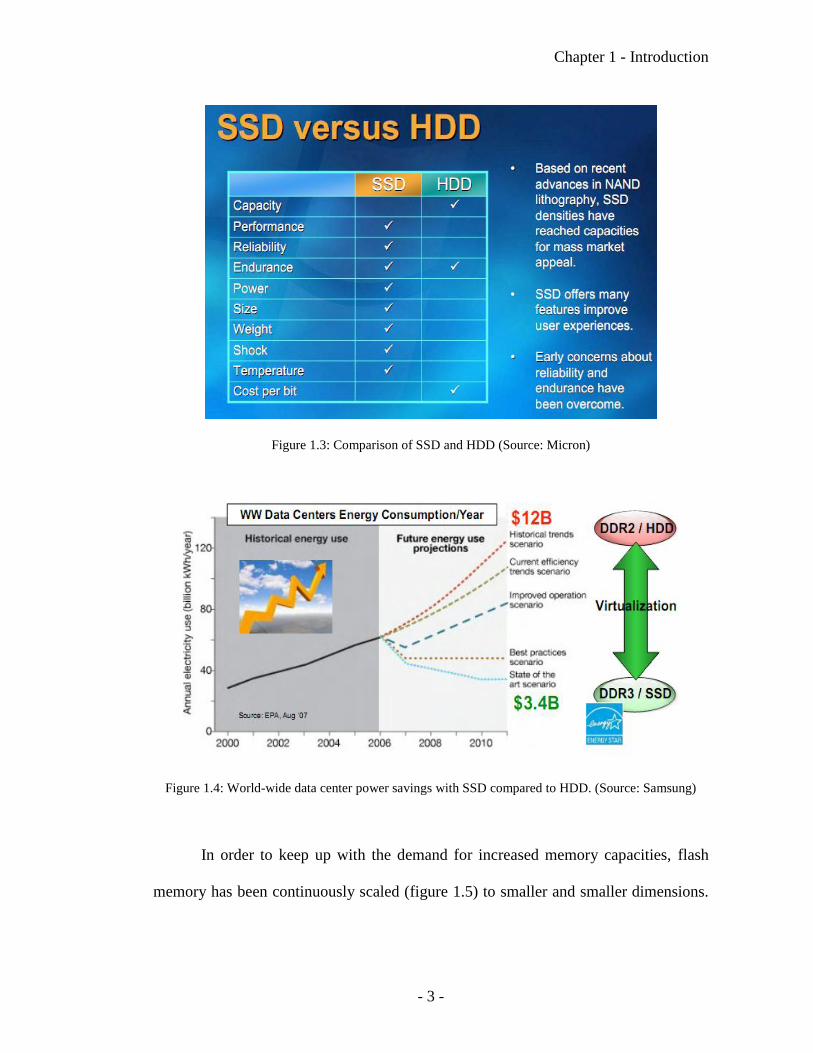
Solid-state drives hold many advantages over HDDs, as shown in figure 1.3. In
addition to providing better performance, SSDs also consume much lesser power than
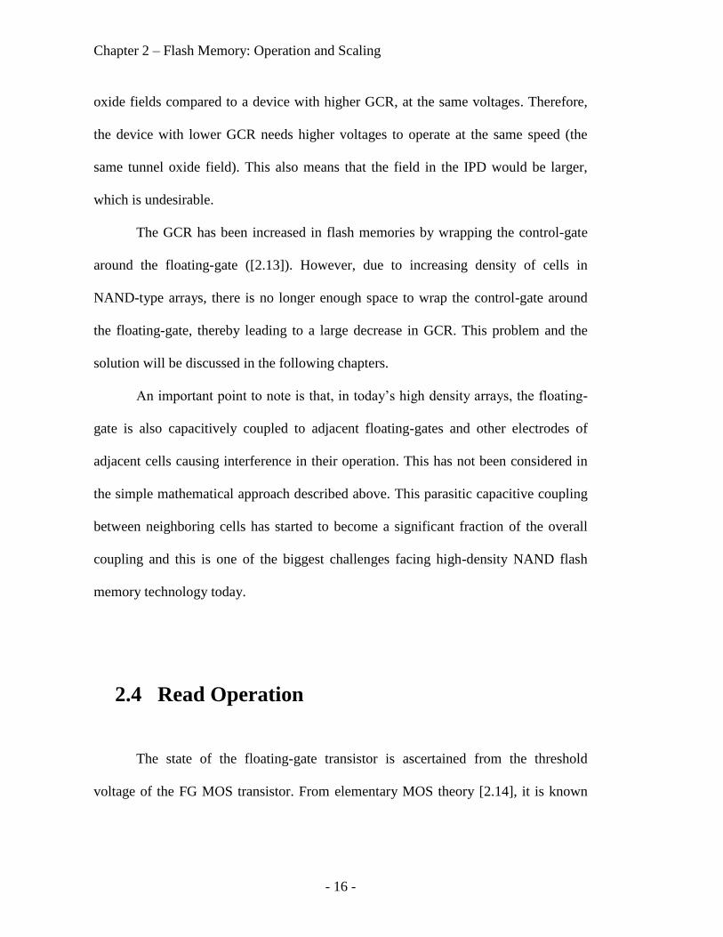
HDDs. This leads to massive savings in power/cost in data servers, shown in figure
1.4.
Chapter 1 - Introduction
- 3 -
Figure 1.3: Comparison of SSD and HDD (Source: Micron)
Figure 1.4: World-wide data center power savings with SSD compared to HDD. (Source: Samsung)
In order to keep up with the demand for increased memory capacities, flash
memory has been continuously scaled (figure 1.5) to smaller and smaller dimensions.

Chapter 1 - Introduction
- 4 -
The scaling of NAND flash memory has been faster than Moore‟s Law [1.3], referred
to as Hwang‟s Law [1.4] but has started to slow down due to difficulties in scaling.
Figure 1.5: Scaling of NAND flash memory. The pace is 2X per year as opposed to 2X every 1.5 years
according to Moore‟s Law. (Source: Samsung)
Further scaling of NAND flash memory faces serious roadblocks. Some of the
biggest challenges include increased parasitic floating-gate (FG) interferences and
decreased gate-coupling ratio (due to lack of space for control-gate (CG) wrap around
the floating-gate) [1.5]. These arise due to the ultra-high density-scaling requirements
of NAND flash memory. This thesis deals with these serious challenges in the
continued scaling of NAND flash memory technology and demonstrates novel
solutions to overcome them.

Chapter 1 - Introduction
- 5 -
1.2 Thesis Organization
This thesis is organized into seven chapters, including this introduction
chapter.
In chapter 2, brief overviews of flash memory history, operation and scaling
are presented. The „floating-gate transistor‟ cell is introduced with its operation
principle. The types of flash memory are described and the main charge injection
mechanisms are discussed. Then, reliability considerations of flash memory are briefly
described, followed by the scaling trends and the main scaling challenges of flash
memory.
Chapter 3 studies poly-silicon floating-gate devices with vertical scaling of the
floating-gate. In the first section, the cell-to-cell interference challenge in scaling
NAND flash memory is discussed, which motivates thickness scaling of the floating-
gate. Subsequently the test structure used for this study, and the fabrication of scaled
poly-silicon floating-gate devices, are described. This is followed by detailed analysis
for the correlation in program/erase/retention characteristics between devices with
poly-silicon floating-gate thicknesses ranging from 75 nm to ultra-thin 7 nm.
In chapter 4, important challenges to the scaling of the poly-silicon floating-
gate thickness are discussed. A new reliability concern, arising from the programming
current increasingly going ballistically through the ultra-thin floating-gate, is
described. A new test structure is developed to experimentally investigate this
phenomenon. Experimental results are presented which quantitatively describe the
magnitude of the effect. The implication of this effect is shown by means of endurance

Chapter 1 - Introduction
- 6 -
data, which show thinner floating-gate devices degrading faster. This reliability
concern poses a major scaling challenge. Following the discussion of this problem,
other issues of doping that limit ultra-thin poly-silicon floating-gates are discussed.
In chapter 5, the use of a metal floating-gate as a replacement for poly-silicon
is explored. The metal floating-gate is experimentally demonstrated to provide
excellent electrical performance. The metal floating-gate can also provide solution to
the ballistic carrier and poly-depletion issues discussed in chapter 4. The factors
underlying the choice of metal are discussed in detail. From the various options
available, TiN (or TaN) is chosen as the preferred floating-gate. The TiN floating-gate
is scaled down to ultra-thin 3 nm, with excellent electrical performance at even such
thicknesses. Utilization of an ultra-thin metallic floating-gate greatly reduces cell-to-
cell interference.
In chapter 6, the replacement of the conventional oxide-nitride control
dielectric with high-k dielectric is explored. The motivation to use high-k control
dielectric is to improve the gate-coupling ratio (GCR), which is lowered as a result of
the inability to wrap the control-gate around the floating-gate. The requirements of the
high-k material for control dielectric application are enumerated. Al2O3 is chosen as
the high-k control dielectric material for experimental demonstration. Poly-silicon
floating-gate devices are integrated with Al2O3 control dielectric, and their electrical
characteristics are presented. The usefulness of a silicon nitride interlayer is proven,
and metal (TaN) floating-gate is integrated with Al2O3 control dielectric. Finally, the
role of the control-gate work-function is discussed.

Chapter 1 - Introduction
- 7 -
In chapter 7, the conclusions and future directions are discussed, in which the
planar floating-gate device is proposed with ultra-thin metal floating-gate, high-k
control dielectric and deep work-function control-gate. Finally, directions for future
research are discussed.

Chapter 1 - Introduction
- 8 -
References
[1.1] R.Barth, “Test challenges beyond 2010”, Proceedings of the Global STC
Conference (GSC), Napa, CA, 14-16 May 2007.
[1.2] Gartner May 2009, Semiconductor Forecast Database (SEQS-WW-DB).
[1.3] G. E. Moore, “Cramming more components onto integrated circuits,”
Electronics, Vol. 38, No. 8, pp. 114-118, April 1965.
[1.4] Hwang‟s Law was named after Hwang Chang-gyu, former head of
Samsung Electronics' semiconductor business.
[1.5] K.Kim et. al., “Memory Technology in the future”, Microelectronic
Engineering, vol.84, p.1976, 2007.

Chapter 2 – Flash Memory: Operation and Scaling
- 9 -
Chapter 2
Flash Memory: Operation and
Scaling
2.1 Introduction
In this chapter, a brief overview of flash memory operation and scaling are
presented, including its short history, the „floating-gate transistor‟ cell and its
operation. The types of flash memory and the main charge injection mechanisms are
discussed. Then, reliability considerations of flash memory are briefly described, with
scaling trends and main scaling challenges.
2.2 What is Flash Memory?
Flash memory is a type of non-volatile memory [2.1]. A non-volatile memory
device is one that can retain stored information in the absence of power (figure 2.1).

Chapter 2 – Flash Memory: Operation and Scaling
- 10 -
Other examples of non-volatile memory include read-only-memory (ROM), hard disk
drives, floppy disks, optical discs etc.
Figure 2.1 : Non-volatile MOS memory qualitative comparison in the flexibility-cost plane (From [2.1])
The first category of non-volatile MOS memories consists of ROMs, in which
the data is permanently written during manufacturing. While these are very
inexpensive, they completely lack flexibility as the data cannot be altered by users.
The first floating-gate memory device was introduced by Kahng and Sze [2.2] in 1967.
In 1970, Frohman-Bentchkowsky [2.3] developed a poly-silicon floating-gate
transistor. In this device, hot electrons are injected into the floating-gate and removed
by ultraviolet (UV) photoemission. This device was called the erasable programmable
read-only memory (EPROM) or UV-EPROM. While this device provided more
flexibility, it needed to be removed from the system to erase it by exposure to UV
light.
Following this, there was a lot of effort to develop electrically erasable
programmable ROMs (EEPROMs) [2.4, 2.5]. The EEPROM cell, consisting of two

Chapter 2 – Flash Memory: Operation and Scaling
- 11 -
transistors and a tunnel oxide was developed. While this had byte-rewrite and erasure
capability, it was a larger cell since it consisted of two transistors.
Subsequently, the flash-EEPROM was developed by Toshiba [2.6] in 1984. A
single-transistor cell was achieved by means of hot carrier programming and tunnel
erase. According to Toshiba, the name "flash" was suggested because the erasure
process of the memory contents reminded them of the flash of a camera.
The first commercial flash memory chip was produced by Intel in 1988 [2.7,
2.8]. This was a NOR-type flash memory chip where there is direct access to each cell.
The first NAND-type flash memory, optimized for higher density, was developed by
Toshiba in 1987 [2.9]. The growth of flash memory was sluggish initially due to
reliability problems but took off dramatically after 2000 due to improvements in
manufacturing process and reliability technology (figure 2.2).
Figure 2.2: Semiconductor memory market for flash, DRAM and SRAM (Source: [2.1], [2.10])

Chapter 2 – Flash Memory: Operation and Scaling
- 12 -
2.3 The Floating-gate Cell
A simple floating-gate transistor cell is shown in Figure 2.3.
Figure 2.3: Cross-section schematic of a floating-gate transistor
A floating-gate transistor is similar to a regular MOS transistor, except for the
additional electrode called the floating-gate and an additional dielectric layer between
the floating-gate and the main gate (or control-gate). The floating-gate is electrically
isolated from surrounding electrodes on all sides by dielectrics. The dielectric layer
between the floating-gate and the control-gate is called the control-dielectric or inter-
poly dielectric (IPD) because both gates are usually made of poly-silicon. The inter-
poly dielectric is typically composed of a triple layer of oxide-nitride-oxide (ONO)
[2.11]. The dielectric closest to the substrate is called the tunnel dielectric (or tunox).
The name originates from the fact that the erase operation and in some cases, the
program operation, occurs through this oxide using quantum mechanical tunneling.

Chapter 2 – Flash Memory: Operation and Scaling
- 13 -
The source and drain are typically n+ type and the substrate is p-type (NMOS
transistor).
The floating-gate serves as the charge storage node. This electrode is
capacitively coupled to the control-gate and other nodes. During the programming
operation, charge is injected into the floating-gate from the substrate using some
mechanism, usually hot-electron injection or tunneling. The charge is sensed as a shift
in the threshold voltage (the turn-on voltage) of the transistor. The charge is removed
from the floating-gate by tunneling through the tunnel oxide back into the substrate.
Figure 2.4 shows the band diagrams for the charged and neutral states of the floating-
gate transistor.
Figure 2.4: Band diagrams for the neutral state (left) and charged state (right) of the floating-gate
transistor. (Source: [2.1])
In the neutral state, there are no electrons on the floating-gate. Electrons are
pushed from the substrate onto the floating-gate during a programming operation. In

Chapter 2 – Flash Memory: Operation and Scaling
- 14 -
the charged state, there are electrons on the floating-gate which raises the potential of
the floating-gate. The potential well formed by the dielectrics on either side of the
floating-gate, enables it to retain charge.
Figure 2.5: Schematic showing the capacitive coupling of the floating-gate (Source [2.12])
Figure 2.5 is a simple schematic of the floating-gate transistor where the
various capacitive couplings to the floating-gate are shown. The floating-gate is
capacitively coupled not only to the control-gate, but also to the source, drain and
body of the transistor. Following [2.12], consider the case when there is no charge on
the floating-gate (Q = 0),
Q = 0 = CFC (VFG – VCG) + CS (VFG – VS) + CD (VFG – VD) + CB (VFG – VB)
Where
CFC is the capacitance between floating-gate and control-gate
CS is the capacitance between floating-gate and source
CD is the capacitance between floating-gate and drain

Chapter 2 – Flash Memory: Operation and Scaling
- 15 -
CB is the capacitance between floating-gate and body
VFG is the potential of the floating-gate
VCG is the potential of the control gate
VD is the potential of the drain
VS is the potential of the source
VB is the potential of the body
If CTot = CFC + CD + CS + CB = Total FG capacitance,
Then
VFG = GCR . VCG + DCR . VD + SCR. VS + BCR. VB
Where
GCR = Gate coupling ratio = CFC / CTot
DCR = Drain coupling ratio = CD / CTot
SCR = Source coupling ratio = CS / CTot
BCR = Body coupling ratio = CB / CTot
2.3.1 Gate coupling ratio (GCR)
The Gate coupling ratio (GCR) is a very important parameter in the design of
flash memories. It is a measure of how strongly the control gate is coupled to the
floating-gate, and as a consequence, it determines the electric fields across the tunnel
oxide and the control oxide. The field across the tunnel oxide is critical to the speed of
operation of the device. A device with a lower GCR would operate at lower tunnel
Chapter 2 – Flash Memory: Operation and Scaling
- 16 -
oxide fields compared to a device with higher GCR, at the same voltages. Therefore,
the device with lower GCR needs higher voltages to operate at the same speed (the
same tunnel oxide field). This also means that the field in the IPD would be larger,
which is undesirable.
The GCR has been increased in flash memories by wrapping the control-gate
around the floating-gate ([2.13]). However, due to increasing density of cells in
NAND-type arrays, there is no longer enough space to wrap the control-gate around
the floating-gate, thereby leading to a large decrease in GCR. This problem and the
solution will be discussed in the following chapters.
An important point to note is that, in today‟s high density arrays, the floating-
gate is also capacitively coupled to adjacent floating-gates and other electrodes of
adjacent cells causing interference in their operation. This has not been considered in
the simple mathematical approach described above. This parasitic capacitive coupling
between neighboring cells has started to become a significant fraction of the overall
coupling and this is one of the biggest challenges facing high-density NAND flash
memory technology today.
2.4 Read Operation
The state of the floating-gate transistor is ascertained from the threshold
voltage of the FG MOS transistor. From elementary MOS theory [2.14], it is known
Chapter 2 – Flash Memory: Operation and Scaling
- 17 -
that a sheet of charge in the gate stack produces a shift in the threshold voltage.
Therefore, following [2.12], we have
ΔVt = shift in threshold voltage = -Q / CFC
Where
Q is the charge on the floating-gate
CFC is the capacitance between CG and FG
And ΔVt is shift in threshold voltage as measured at the CG
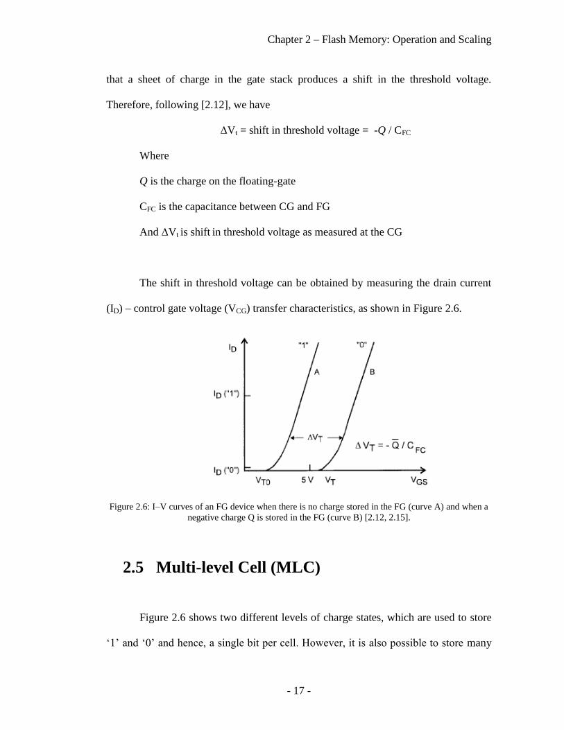
The shift in threshold voltage can be obtained by measuring the drain current
(ID) – control gate voltage (VCG) transfer characteristics, as shown in Figure 2.6.
Figure 2.6: I–V curves of an FG device when there is no charge stored in the FG (curve A) and when a
negative charge Q is stored in the FG (curve B) [2.12, 2.15].
2.5 Multi-level Cell (MLC)
Figure 2.6 shows two different levels of charge states, which are used to store
„1‟ and „0‟ and hence, a single bit per cell. However, it is also possible to store many

Chapter 2 – Flash Memory: Operation and Scaling
- 18 -
more levels of charge in a cell. For example, a cell with 4 levels of charge states can
be used to store „11‟, „10‟, „01‟ and „00‟, thereby storing 2 bits per cell (figure 2.7).
Similarly, a cell with 8 levels of charge states can store 3 bits per cell. In general, a
cell with „2n‟ charge states can store „n‟ bits per cell [2.11, 2.13].
Figure 2.7 : Two different threshold voltage states lead to 1 bit per cell storage while four different
threshold voltage states lead to 2 bits per cell.
While multi-level cells are very important and useful in increasing density of
storage in flash memories, they also make design much more restrictive and stringent
due to the smaller window available between adjacent threshold voltage states [2.13].
2.6 Types of Flash Memory
There are two main types of flash memory in use today, called NOR flash
memory [2.6] and NAND flash memory [2.9]. While both are based on the floating-
gate transistor cell, their principal difference is in the way the cells are connected
together in an array. The words „NOR‟ and „NAND‟, refer to the NOR-gate type and
NAND-gate type connections of the cells in an array. Figure 2.8 shows NOR and
NAND-type flash memory arrays.

Chapter 2 – Flash Memory: Operation and Scaling
- 19 -
From the figure, we can see that there is direct access to each cell in NOR-type
flash memory. The control-gate electrode is connected to the word-line and the drain
is connected to the bit-line. The sources are grounded. The NAND-type cell cross-
section is similar except for the contacts. The contact corresponding to each cell is
eliminated in the interest of higher packing density. However, the direct cell access
present in NOR-type memory is not available in NAND-type memory. Hence, the
latency for random access in NAND flash is much longer (1-10 microseconds)
compared to NOR flash (10s of nanoseconds) due to the larger resistance of the line
discharging the bit-line capacitance [2.11].
Figure 2.8 : NOR and NAND flash arrays with layout comparison (Source: Intel [2.11])

Chapter 2 – Flash Memory: Operation and Scaling
- 20 -
The differences between NOR and NAND-type flash memories [2.11] are
shown in Table 2.1.
NOR Flash Memory NAND Flash Memory
Cell size = 10λ2 Cell size = 5λ
2
Direct access to cell Indirect access to cell
Fast random access Slow random access. Fast page access
Slower Program/Erase Faster Program/erase
Channel hot electron programming Fowler-Nordheim tunneling programming
Byte addressable I/O type interface
Lower density Higher density
Used for code-storage applications, which
require execution-in-place (XIP)
Used for data-storage applications, like
media players, which require fast
program/erase and fast page access
Table 2.1: Major differences between NOR and NAND flash memories
Therefore, NAND flash memories are well-suited for data-storage applications
like media players, cameras and solid-state drives, while NOR flash memories are
better suited for storing and executing operating system code in cellular phones. Since
NAND flash memories are experiencing a dramatic increase in demand [2.16] for very
high density storage, they are the main technological driver. Hence, the problems and
solutions discussed in this thesis are focused on NAND flash memory.

Chapter 2 – Flash Memory: Operation and Scaling
- 21 -
The mechanisms of charge injection are different in NOR and NAND flash
memories, and this is critical to the operation of the floating-gate transistor. The two
most commonly used mechanisms of charge injection are described in the next
section.
2.7 Mechanisms of Charge Injection
In this section, two main types of charge injection mechanisms are discussed.
Channel hot electron (CHE) injection is used to program NOR flash memory, while
Fowler-Nordheim (F-N) tunneling is used to program NAND flash memory. Both
NOR and NAND flash memories are erased using F-N tunneling. These mechanisms
are briefly described below.
2.7.1 Channel hot electron (CHE) injection
In CHE injection ([2.18], [2.19], [2.20], [2.21], [2.22]), the basic idea is to
provide enough energy to the channel electrons to overcome the tunnel oxide – silicon
energy barrier. A large drain voltage produces a lateral electric field (between source
and drain). This field increases the energy of the electrons, thus making them „hot‟.
The drain voltage needs to be higher than the oxide-silicon barrier (3.2 eV). These hot
electrons are injected from the channel into the floating-gate, due to the perpendicular
field applied from the gate. This injection primarily happens near the drain, because

Chapter 2 – Flash Memory: Operation and Scaling
- 22 -
that is the region where the electrons have gained maximum energy, or are the
„hottest‟. A NOR flash programming operation using CHE injection is depicted in Fig
2.9.
Figure 2.9 : NOR flash programming using CHE injection [Source: Intel]
Hot-electron injection is commonly described using the „lucky-electron‟ model
[2.21]. This is based on the premise that the electron needs to be „lucky‟ to be injected
because it should have sufficient energy higher than the barrier, which means that it
should not suffer too many scattering events that reduce its energy while it moves
from the source to the drain. In addition, the momentum of the electron should be
directed towards the interface, possibly by a scattering event. Since the probability of
such conditions is very low, the electron which does satisfy these conditions is „lucky‟.
This also implies that hot electron injection is an inefficient method of programming
since only a tiny fraction of channel electrons end up getting injected. The band
diagram is depicted in Fig. 2.10 along with the slight lowering of the barrier due to the
Schottky barrier (image charge) lowering effect [2.22].

Chapter 2 – Flash Memory: Operation and Scaling
- 23 -
Figure 2.10 : A schematic energy band diagram describing the three processes involved in electron
injection [2.22]
More advanced quasi-thermal equilibrium models exist for describing CHE
injection ([2.12], [2.17], [2.23], [2.24]).
2.7.2 Fowler-Nordheim tunneling
Fowler–Nordheim (F-N) tunneling [2.25] refers to quantum-mechanical
tunneling through a thin potential barrier, induced by an electric field. Figure 2.11
shows F-N tunneling from the poly-silicon FG into the substrate. The oxide band
bends under the application of an electric field, and presents a triangle-shaped barrier
to the FG. The larger the field, the thinner the tunneling barrier is, so the current is
larger. The probability of tunneling also depends on the distribution of carriers in the
injecting material and the height of the barrier. Unlike the „lucky electron‟ hot carrier
injection discussed earlier, F-N tunneling injection is 100% efficient.

Chapter 2 – Flash Memory: Operation and Scaling
- 24 -
Figure 2.11 : F-N tunneling of electrons from the poly-Si FG into the Si substrate through the triangular
energy barrier posed by the tunox. (Source: [2.12])
Using a free-electron gas model for the metal and the Wentzel–Kramers–
Brillouin (WKB) approximation for the tunneling probability [2.25, 2.26, 2.37], the
following expression for current density is obtained:
Where
J = Current density
E = Electric field across the dielectric

Chapter 2 – Flash Memory: Operation and Scaling
- 25 -
e = electronic charge
2πh = Planck‟s constant
Φ0 = Barrier height
mox = electron mass in oxide
m = free electron mass
Figure 2.12 shows F-N tunneling current as a function of electric field. The
current is exponentially dependent on the field. This is important, because at low fields
when we just want to retain charge, the tunneling current is very low, and at high
fields the current is very high which enables fast charge injection.
Figure 2.12 : F-N tunneling current as a function of electric field (Source: [2.12], [2.27])

Chapter 2 – Flash Memory: Operation and Scaling
- 26 -
The classic expression for F-N current density shown above does not consider
some issues: the temperature dependence of the phenomenon, the quantum effects at
the silicon interface, the influence of band bending at the Si/SiO2 interface, and the
voltage drop in silicon, the fact that the correct statistics for electrons are not
Maxwellian but Fermi–Dirac, and the collision-broadening barrier lowering [2.12,
2.28].
In the case of poor quality oxides [2.29] that contain large numbers of bulk and
interface traps, trap-assisted tunneling [2.30] increases tunneling current density to
much greater values than expected due to the effective decrease in barrier.
Figure 2.13 shows a NAND flash memory device programmed by F-N
tunneling.
Figure 2.13: F-N programming in NAND flash (Source [2.11])

Chapter 2 – Flash Memory: Operation and Scaling
- 27 -
2.8 Reliability of Flash Memories
So far, the basic structure and operation of the floating-gate device has been
described along with the two main types of flash memory – NOR and NAND. These
descriptions have established the mechanisms through which charge is injected and
removed from the floating-gate and the means of reading the state of the device. In
this section, a very important issue in flash memory technology is discussed – the
reliability [2.31].
2.8.1 Endurance (Cycling)
The flash memory device is required to retain its properties on being subjected
to repeated program/erase cycles. When thin dielectrics are repeatedly stressed at high
fields, interface and bulk traps develop in the dielectric [2.29]. Charge is trapped and
released from these traps, and this modifies the fields across the dielectric. This tends
to modify the program/erase characteristics over time, as damage is induced in the
dielectric. Figure 2.14 shows the threshold voltage window closing with cycling due to
traps induced in the tunnel oxide.

Chapter 2 – Flash Memory: Operation and Scaling
- 28 -
Figure 2.14 : Threshold voltage window closure caused by traps in the tunnel oxide as a function of
program/erase cycles on a single cell, showing endurance characteristics [2.1].
Flash memories are typically expected to last for 100,000 cycles [2.13] without
major degradation. Modern multi-level cells have lower endurance benchmarks due to
extremely stringent threshold voltage windows.
2.8.2 Retention
The „retention‟ [2.32] is critical in any non-volatile memory device. The ability
to retain charge without supplied power is the definition of non-volatile memory.
„Retention‟ is a benchmark used to quantify the extent of time for which the stored
charge is retained in a device. Figure 2.15 shows the band diagram of a flash memory
device in the charge-retention state.

Chapter 2 – Flash Memory: Operation and Scaling
- 29 -
Figure 2.15: Band diagram showing charge-retention state and leakage path through dielectrics
The charge-loss in the retention state is determined by tunneling leakage under
weak fields through adjoining dielectrics. This charge-loss would be greatly amplified
if the dielectrics contained defects, since that would enhance trap-assisted tunneling
[2.30].
A typical retention benchmark for flash memories is 10 years [2.13], i.e. the
floating-gate device should not lose more than a small fraction of its carriers for 10
years. In practice, it is not possible to quantify retention by doing measurements for
such a long period of time. Hence, retention tests are accelerated at higher
temperatures. Typically, a 24-hour benchmark at 150 °C is utilized. Loss of charge
with time at higher temperatures is measured to make a comparison of retention
properties of the devices under study. Mean times to failure and defect density are
other metrics used for quantifying reliability of flash memory [2.33].

Chapter 2 – Flash Memory: Operation and Scaling
- 30 -
2.9 Flash Memory Scaling
Flash memories, like most other electronic devices, have been continually
scaled since their introduction, to obtain increasing densities.
Figure 2.16 : NOR flash memory scaling (Source: Intel [2.11])
NOR-type flash memories were the first to be introduced. Figure 2.16 shows
the scaling of NOR flash memory for two decades. Until recently, non-volatile
memory half-pitches have lagged those for DRAM or CMOS logic devices in the
same year [2.13]. Rapid progress in NAND flash technology has not only reversed this
trend, but also surpassed the half-pitches of DRAM and CMOS logic devices. NAND
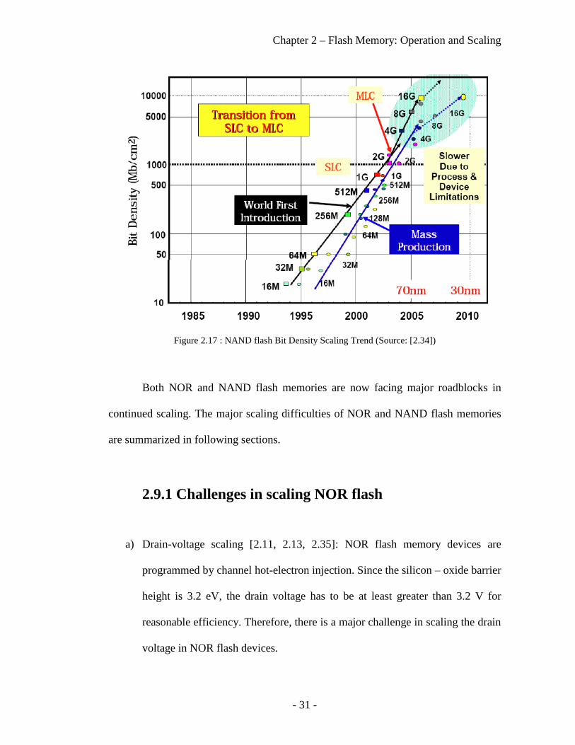
flash memories have seen tremendous demand in this decade, and their bit density
scaling trend is shown in Figure 2.17.
Chapter 2 – Flash Memory: Operation and Scaling
- 31 -
Figure 2.17 : NAND flash Bit Density Scaling Trend (Source: [2.34])
Both NOR and NAND flash memories are now facing major roadblocks in
continued scaling. The major scaling difficulties of NOR and NAND flash memories
are summarized in following sections.
2.9.1 Challenges in scaling NOR flash
a) Drain-voltage scaling [2.11, 2.13, 2.35]: NOR flash memory devices are
programmed by channel hot-electron injection. Since the silicon – oxide barrier
height is 3.2 eV, the drain voltage has to be at least greater than 3.2 V for
reasonable efficiency. Therefore, there is a major challenge in scaling the drain
voltage in NOR flash devices.
Chapter 2 – Flash Memory: Operation and Scaling
- 32 -
b) Tunnel oxide scaling [2.13, 2.35]: The scaling of tunnel oxide is limited by
concerns for reliability issues. Since NOR flash memories provide direct cell
access, the reliability issues are more stringent, unlike NAND flash memories
which can use error code correction and data re-mapping strategies. The tunnel
oxide thickness for NOR flash devices is essentially stuck at 8-9 nm and not
scaled anymore.
c) Channel length scaling [2.13, 2.35]: There are a number of factors contributing
to difficulty in scaling channel length in NOR flash devices. NOR flash
devices use abrupt drain junctions to generate high lateral fields, which in turn
are required to efficiently generate hot electrons. However, these abrupt
junctions also increase short-channel effects and leakage current. Use of halo
implants helps with leakage but reduces junction breakdown voltage. All this is
exacerbated by the fact that the tunnel oxide does not scale anymore, because a
thinner tunnel oxide reduces short-channel effects. Hence, the channel length
faces potentially game-ending scaling issues and consequently, so does the cell
area.
d) Control Dielectric scaling [2.35]: This is also limited by reliability concerns,
similar to the tunnel oxide.
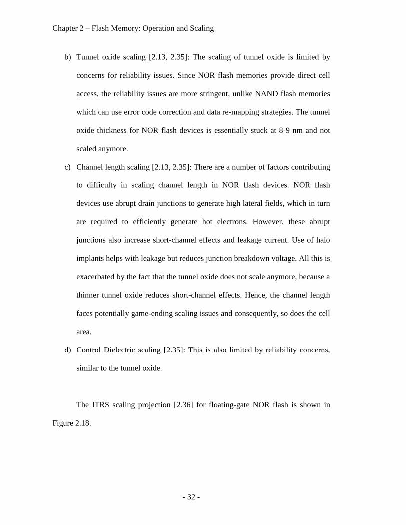
The ITRS scaling projection [2.36] for floating-gate NOR flash is shown in
Figure 2.18.
Chapter 2 – Flash Memory: Operation and Scaling
- 33 -
Figure 2.18: NOR flash ITRS Scaling Projection [2.36]
2.9.2 Challenges in scaling NAND flash
a) Cell-to-cell interference [2.13, 2.35]: The scaling of high-density NAND flash
memory is limited by parasitic interference between adjacent cells since they
are extremely close to each other. The floating-gate, being a capacitive-
coupled electrode, has started to have significant coupling with the floating-

Chapter 2 – Flash Memory: Operation and Scaling
- 34 -
gates of adjacent cells and other electrodes of neighboring cells. This causes an
undesirable shift in the state of one cell due to neighboring cells. Especially
with the advent of multi-level cells, the window between states is not much,
which is the biggest challenge in the scaling of NAND flash memory.
b) Maintaining GCR [2.13]: A GCR > 0.6 is necessary for satisfactory operation
of these devices, and this is typically achieved by wrapping the control-gate
around the floating-gate, thereby increasing the area and consequently the
capacitive coupling between the two gates. However, with decreasing spacing
between adjacent cells, there is no longer any space for wrapping the control-
gate in between floating-gates. This leads to significant reduction in the GCR
and needs to be compensated by some method.
c) Tunnel oxide scaling [2.13, 2.35]: Like NOR flash, tunnel oxide scaling in
NAND flash is also limited by reliability concerns. However, due to the use of
error correction codes (ECC), NAND flash is a little more tolerant to tunnel
oxide scaling than NOR flash. Still, the tunnel oxide thickness is stuck at ~6
nm and needs breakthroughs to continue scaling beyond that.
d) Control dielectric scaling [2.36]: The control dielectric thickness is also limited
by reliability concerns, similar to the tunnel oxide. Reliability concerns are also
very serious if the control dielectric is modified to use high-k dielectrics, which
may be necessary to improve GCR.
e) Lithography concern [2.35]: Lithography limitations are also an important
problem in further scaling of NAND flash. Extreme ultraviolet (EUV)
lithography is the main candidate for next generation lithography.

Chapter 2 – Flash Memory: Operation and Scaling
- 35 -
f) Few electron phenomena [2.35]: The ultimate intrinsic limits of NAND flash
memories are likely to be due to statistical fluctuations induced by too few
electrons stored.
Figure 2.19 shows the ITRS scaling projections for floating-gate NAND flash
memory.

Chapter 2 – Flash Memory: Operation and Scaling
- 36 -
Figure 2.19 : ITRS Scaling projections for floating-gate NAND flash. [2.36]

Chapter 2 – Flash Memory: Operation and Scaling
- 37 -
References
[2.1] R. Bez, E. Camerlenghi, A. Modelli, and A. Visconti, “Introduction to
flash memory,” Proceedings of the IEEE, Vol. 91, No. 4, April 2003.
[2.2] D. Kahng and S.M. Sze, “A floating gate and its application to memory
devices”, IEEE Trans. Electron Devices, Vol. 9, Issue 9, p. 629, 1967.
[2.3] D. Frohman-Bentchkowsky, “Memory behavior in a floating-gate
avalanche injection MOS (FAMOS) structure,” Appl. Phys. Lett., Vol. 18, pp. 332–
334, 1971.
[2.4] Iizuka, H., Masuoka, F., Sato, T., and Ishikawa, M. (1976) Electrically
alterable avalanche-injection type MOS read-only memory with stacked-gate
structures. IEEE Transactions on Electron Devices. ED-23, 379.
[2.5] D. C. Guterman, I. H. Rimawi, T. L. Chiu, R. D. Halvorson, and D. J.
McElroy, “An electrically alterable nonvolatile memory cell using a floating gate
structure”, IEEE Trans. Electron Devices, Vol. 26, p. 576, 1979.
[2.6] F. Masuoka, M. Asano, H. Iwahashi, T. Komuro, and S. Tanaka, “ A new
Flash E2PROM cell using triple polysilicon technology,” in IEDM Tech. Dig., p. 464,
1984.
[2.7] G. Verma and N. Mielke, “Reliability performance of ETOX based Flash
memories,” Proc. IRPS, p. 158, 1988.
[2.8] P. Cappelletti, C. Golla, P. Olivo, and E. Zanoni, “Flash Memories”,
Kluwer Academic Publishers, MA, 1999.

Chapter 2 – Flash Memory: Operation and Scaling
- 38 -
[2.9] F. Masuoka et. al., “New ultra high density EPROM and flash EEPROM
with NAND structure cell”, IEDM Tech. Digest, 1987.
[2.10] Webfeet Inc., “Semiconductor industry outlook,” presented at the 2002
Non-Volatile Memory Conference, Santa Clara, CA, 2002.
[2.11] A.Fazio (Intel), “Challenges in charge based flash memory & phase
change memory”, EE310 Seminar, Stanford University, January 2007.
[2.12] P. Pavan, R. Bez, P. Olivo, and E. Zanoni, “Flash memory cells - An
overview,” Proceedings of the IEEE, Vol. 85, No. 8, August 1997.
[2.13] International Technology Roadmap for Semiconductors: Process
Integration, Devices and Structures, 2009 edition.
[2.14] Robert Pierret, "Semiconductor Device Fundamentals", Addison Wesley
Publishing Company (1996).
[2.15] M. Woods, “An E-PROM‟s integrity starts with its cell structure,” in
Nonvolatile Semiconductor Memories: Technologies, Design, and Application, C. Hu,
Ed. New York: IEEE Press, pp. 59-62, 1991.
[2.16] Gartner May 2009, Semiconductor Forecast Database (SEQS-WW-DB).
[2.17] C. C. Yeh et. al., “PHINES: A novel low power program/erase, small
pitch, 2-Bit per cell flash memory,” IEDM Tech. Dig., pp. 931-934, 2002.
[2.18] S. Wolf “Silicon Processing for the VLSI era”, vol. 3, Lattice Press,
1995.
[2.19] P. B. Kumar et. al., “Lateral profiling of trapped charge in SONOS flash
EEPROMs programmed using CHE injection,” IEEE Trans. Electron Devices, Vol.
53, No.4, pp. 698–705, 2006.

Chapter 2 – Flash Memory: Operation and Scaling
- 39 -
[2.20] B. Eitan and D. Froham-Bentchkowsky, “Hot-electron injection into the
oxide in n-channel MOS devices,” IEEE Trans. Electron Devices, Vol. ED-28, No. 3,
pp. 328-340, 1981.
[2.21] C. Hu, “Lucky-electron model for channel hot-electron emission,”
IEDM Tech. Dig., p. 22, 1979.
[2.22] S. Tam, P. K. Ko, C. Hu, and R. Muller, “Correlation between substrate
and gate currents in MOSFET‟s,” IEEE Trans. Electron Devices, Vol. ED-29, No. 11,
pp.1740-1744, 1982.
[2.23] E. Takeda, H. Kune, T. Toyabe, and S. Asai, “Submicrometer MOSFET
structure for minimizing hot-carrier generation,” IEEE Trans. Electron
Devices, Vol.ED-29, No. 4, pp. 611-618, 1982.
[2.24] K. Hess and C. T. Sah, “Hot carriers in Silicon surface inversion layers,”
J.Appl. Phys., Vol. 45, p. 1254, 1974.
[2.25] M. Lenzlinger and E. Snow, “Fowler Nordheim tunneling in thermally
grown SiO2,” J. Appl. Phys., Vol. 40, p. 278, 1969.
[2.26] R.K.Chanana et.al., “Fowler–Nordheim hole tunneling in p-SiCÕSiO2
structures”, Applied Physics Letters, Vol.77, No.16 (Oct 2000).
[2.27] “IEDM 90 short course: Non-volatile memory,” IEEE, San Francisco,
CA, 1990.
[2.28] Tang and K. Hess, “Theory of hot electron emission from silicon
into silicon dioxide,” J. Appl. Phys., vol. 54, pp. 5145–5151, 1983.
[2.29] P. Olivo, T. Nguyen, and B. Ricc`o, “High-field-induced degradation

Chapter 2 – Flash Memory: Operation and Scaling
- 40 -
in ultra thin SiO2 films,” IEEE Trans. Electron Devices, vol. 35, no. 12, pp.
2259–2267, 1988.
[2.30] L. Larcher, “Statistical simulation of leakage current in MOS and flash
memory devices with a new multiphonon trap-assisted tunneling model,” IEEE Trans.
Electron Devices, Vol. 50, No. 5, pp. 1246-1253, 2003.
[2.31] C. Cappelletti, R. Bez, A. Modelli, and A. Visconti, “What we have
learned on flash memory reliability in the last ten years,” IEDM Tech. Dig., pp. 489-
492, Dec. 2004.
[2.32] C. M. Compagnoni, D. Ielmini, A. S. Spinelli, A. L. Lacaita, C.
Previtali, and C.Gerardi, “ Study of data retention for nanocrystal flash memories,”
IEEE 41st Annual International Reliability Physics Symposium Proceedings, pp. 506-
512, 2003.
[2.33] P. Cappelletti, C. Golla, P. Olivo, and E. Zanoni, Flash Memories,
Kluwer Academic Publishers, MA, 1999.
[2.34] C. Kim, “Future Memory Technology: Trends and Challenges,” Plenary
paper, ISQED (2006).
[2.35] Barbara De Salvo, Silicon non-volatile memories: paths of innovation,
ISTE John Wiley 2009.
[2.36] ITRS Table PIDS5, 2009.
[2.37] Z. A. Weinberg, “On tunneling in metal-oxide-silicon structures”,
Journal of Applied Physics, Vol. 53, 5052, 1982.

Chapter 3 – Scaled Poly-Silicon Floating-Gate NAND Flash Memory
- 41 -
Chapter 3
Scaled Poly-Silicon Floating-Gate
NAND Flash Memory
3.1 Introduction
This chapter studies poly-silicon floating-gate devices with vertical scaling, i.e,
thickness scaling of the floating-gate. In the first section, the cell-to-cell interference
challenge in scaling NAND flash memory is discussed, which motivates thickness
scaling of the floating-gate. Subsequently the test structure used for this study, and the
fabrication of scaled poly-silicon floating-gate devices are described. This is followed
by the results of the study comparing and discussing in detail the program/erase and
retention characteristics of devices with poly-silicon floating-gates of various
thicknesses ranging from 75 nm to ultra-thin 7 nm.

Chapter 3 – Scaled Poly-Silicon Floating-Gate NAND Flash Memory
- 42 -
3.2 Motivation
3.2.1 Cell-to-cell interference
NAND flash memory is optimized for use with high-density
applications [3.1, 3.2, 3.3, 3.4, 3.5]. As the density gets higher and higher, the
floating-gate cells get closer and closer to each other. The floating-gate, being
a capacitive-coupled electrode, has started to have significant coupling with the
floating-gates of adjacent cells and other electrodes of neighboring cells [3.2,
3.4, 3.5, 3.12]. Figure 3.1 shows an SEM image of a NAND flash array
showing the parasitic coupling between cells.
Figure 3.1: SEM of NAND flash array (Source: [3.7])
This causes an undesirable shift in the state of one cell due to
neighboring cells (figure 3.2).

Chapter 3 – Scaled Poly-Silicon Floating-Gate NAND Flash Memory
- 43 -
Figure 3.2 : Floating-gate interference causes undesirable shift in threshold voltage of one cell due to
adjacent cells (Source: [3.7])
The undesirable shift in state of a cell due to capacitive coupling with
adjacent cells in the array (in the bit-line direction), is depicted in figure 3.3.
With multi-level cells (MLC), the design window available for the threshold
voltage states is much reduced due to the need to accommodate a large number
of states in a single cell. Figure 3.4 depicts the interference problem getting
worse with technology node scaling and shows the relative magnitudes of the
interference along different directions. This is one of the biggest challenges in
the further scaling of NAND flash memory.

Chapter 3 – Scaled Poly-Silicon Floating-Gate NAND Flash Memory
- 44 -
Figure 3.3: This figure depicts the shifting of threshold voltage of Cell 1 when Cell 2 gets programmed
due to the parasitic coupling between the adjacent cells. (Source: [3.6])
Figure 3.4: The undesirable threshold voltage shift (interference) is getting worse with scaling. (Source:
[3.8], [3.9])
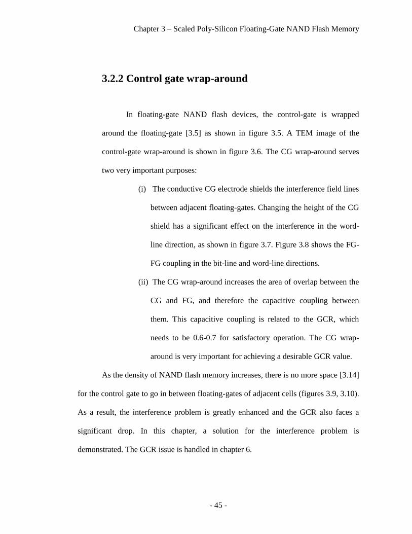
Chapter 3 – Scaled Poly-Silicon Floating-Gate NAND Flash Memory
- 45 -
3.2.2 Control gate wrap-around
In floating-gate NAND flash devices, the control-gate is wrapped
around the floating-gate [3.5] as shown in figure 3.5. A TEM image of the
control-gate wrap-around is shown in figure 3.6. The CG wrap-around serves
two very important purposes:
(i) The conductive CG electrode shields the interference field lines
between adjacent floating-gates. Changing the height of the CG
shield has a significant effect on the interference in the word-
line direction, as shown in figure 3.7. Figure 3.8 shows the FG-
FG coupling in the bit-line and word-line directions.
(ii) The CG wrap-around increases the area of overlap between the
CG and FG, and therefore the capacitive coupling between
them. This capacitive coupling is related to the GCR, which
needs to be 0.6-0.7 for satisfactory operation. The CG wrap-
around is very important for achieving a desirable GCR value.
As the density of NAND flash memory increases, there is no more space [3.14]
for the control gate to go in between floating-gates of adjacent cells (figures 3.9, 3.10).
As a result, the interference problem is greatly enhanced and the GCR also faces a
significant drop. In this chapter, a solution for the interference problem is
demonstrated. The GCR issue is handled in chapter 6.

Chapter 3 – Scaled Poly-Silicon Floating-Gate NAND Flash Memory
- 46 -
Figure 3.5: Control-gate is wrapped around the FG shielding interference between adjacent floating-
gates
Figure 3.6: Image showing CG wrapping around the FG [3.10]
FG FG
Control gate
Control gate wrapped around
Floating gate shielding FG-FG interference

Chapter 3 – Scaled Poly-Silicon Floating-Gate NAND Flash Memory
- 47 -
Figure 3.7: Changing the height of the CG wrap-around has a significant effect on the word-line
direction interference [3.10]
Figure 3.8 : Interference along BL direction and WL direction [3.11]
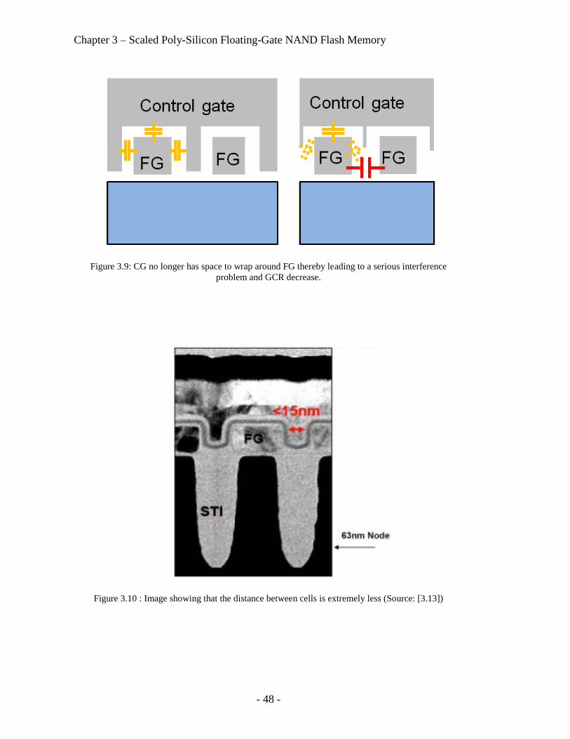
Chapter 3 – Scaled Poly-Silicon Floating-Gate NAND Flash Memory
- 48 -
Figure 3.9: CG no longer has space to wrap around FG thereby leading to a serious interference
problem and GCR decrease.
Figure 3.10 : Image showing that the distance between cells is extremely less (Source: [3.13])

Chapter 3 – Scaled Poly-Silicon Floating-Gate NAND Flash Memory
- 49 -
3.3 Floating-gate thickness scaling
The parasitic interference between adjacent cells can be lowered by reducing
the thickness of the floating-gate [3.15, 3.16, 3.17]. Figure 3.11 shows that by
reducing the thickness of the floating-gate, we reduce the area of overlap between the
FG and interfering electrodes, thereby reducing the capacitive coupling and the
interference between them. Figure 3.12 indicates that we need floating-gate
thicknesses to be on the order of a few nm, to meet interference requirements for
future nodes. Conventional NAND flash memory devices use poly-silicon floating-
gates of thickness ~45 nm ([3.10]). Here, we systematically study the scaling of the
poly-silicon floating gate by fabricating devices with floating-gate thicknesses going
from 75 nm to ultra-thin 7 nm and comparing their electrical characteristics.
Figure 3.11: Reduction of FG height greatly reduces FG interference.

Chapter 3 – Scaled Poly-Silicon Floating-Gate NAND Flash Memory
- 50 -
Figure 3.12: Shows that for future nodes, required FG height is a few nm. (Source: [3.16])
3.4 Experimental Test Structure
The purpose of the experiment is to fabricate and study floating-gate devices
with a range of floating-gate thicknesses varying from thick 75 nm floating-gate to as
thin as possible. The devices need to be compared in terms of program/erase
characteristics, retention and endurance. The floating-gate capacitor shown in Figure
3.13 is chosen as the test structure.

Chapter 3 – Scaled Poly-Silicon Floating-Gate NAND Flash Memory
- 51 -
A capacitor is chosen instead of a transistor because the capacitor enables the
study of program/erase characteristics, retention and endurance with reduced
complexity of fabrication compared to the transistor. The state of the device is sensed
by measuring the flat-band voltage from a capacitance-voltage sweep.
An important thing to note from Figure 3.13 is the emulated control gate wrap-
around. The area between the control gate and the floating gate is fixed while the area
between the floating-gate and channel has been made smaller, by modifying the active
area size. By doing this, the increased area between the CG and FG mimics the
control-gate wrapping around the floating-gate in NAND flash memory devices. This
Figure 3.13: Schematic of experimental test structure
Chapter 3 – Scaled Poly-Silicon Floating-Gate NAND Flash Memory
- 52 -
enables study of the devices with a range of GCR values since the GCR value is a
function of the ratio of the IPD capacitance and the tunox capacitance.
Since the structure is a capacitor, minority carriers need to be generated and do
not have a source, like in a transistor. This means that the generation of minority
carriers will take time, and hence the erase operation can not be performed at speeds
faster than 1 ms in the case of n-type substrate. There is a similar restriction on
programming speed in the case of p-type substrate. This is because the substrate goes
into deep depletion when the appropriate bias is applied, implying that most of the
voltage applied drops across the substrate and not the tunnel oxide field. By giving
sufficient time for the minority carriers to be generated, the substrate goes from deep
depletion to inversion, making the tunnel oxide field as high as expected.
3.5 Fabrication
The starting substrate is an (100) 1-5 Ω cm n-type silicon substrate. The device
isolation is performed by growing a 0.5 micron thick thermal oxide and opening up
active areas with a wet buffered oxide etch. Following that, the tunnel oxide is grown
in dry oxygen at 800 °C to obtain ~7 nm oxide. This thickness is limited by reliability
concerns. Following this, the critical step of poly-silicon floating-gate deposition is
performed.

Chapter 3 – Scaled Poly-Silicon Floating-Gate NAND Flash Memory
- 53 -
The smoothness and quality of the poly-silicon floating-gate are very important
to the functionality of the floating-gate device. A rougher poly-silicon floating-gate
would result in a leakier oxide on top on it [3.18]. To obtain smoother layers, the
floating-gate can be deposited in amorphous form and subsequently crystallized.
Therefore, the deposition of amorphous silicon is performed at 580 °C in-situ doped
with phosphorus as high as possible. Annealing at high temperatures can cause
significant grain growth and roughen the surface. Hence, the annealing step is
postponed until after the IPD stack is deposited so that the roughness of the floating-
gate under the stack does not get affected much.
Following the deposition of the amorphous silicon, a thin 20 nm capping layer
of low temperature silicon oxide (LTO) is deposited at 300 °C to protect the floating-
gate surface during subsequent processing. The floating-gate is patterned and dry
etched in an SF6/O2 plasma. The capping LTO is removed and the IPD stack
deposition begins.
A well-characterized LTO of reproducible quality is deposited at 450 °C and
annealed at 750 °C in dry oxygen to enhance its quality. Following this, silicon nitride
is deposited at 785 °C. Following that, another step of LTO deposition is performed,
followed by another anneal at 750 °C in dry oxygen and an anneal at 950°C in
nitrogen. The 950 °C nitrogen anneal also serves to activate the dopants in the
floating-gate in addition to improving the quality of the IPD stack. All these higher
temperature steps also help crystallize the amorphous silicon into poly-silicon. Since
the crystallization occurs with the IPD stack on top of the floating-gate, it is less likely
to be roughened during the process.
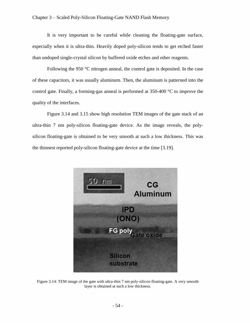
Chapter 3 – Scaled Poly-Silicon Floating-Gate NAND Flash Memory
- 54 -
It is very important to be careful while cleaning the floating-gate surface,
especially when it is ultra-thin. Heavily doped poly-silicon tends to get etched faster
than undoped single-crystal silicon by buffered oxide etches and other reagents.
Following the 950 °C nitrogen anneal, the control gate is deposited. In the case
of these capacitors, it was usually aluminum. Then, the aluminum is patterned into the
control gate. Finally, a forming-gas anneal is performed at 350-400 °C to improve the
quality of the interfaces.
Figure 3.14 and 3.15 show high resolution TEM images of the gate stack of an
ultra-thin 7 nm poly-silicon floating-gate device. As the image reveals, the poly-
silicon floating-gate is obtained to be very smooth at such a low thickness. This was
the thinnest reported poly-silicon floating-gate device at the time [3.19].
Figure 3.14: TEM image of the gate with ultra-thin 7 nm poly-silicon floating-gate. A very smooth
layer is obtained at such a low thickness.
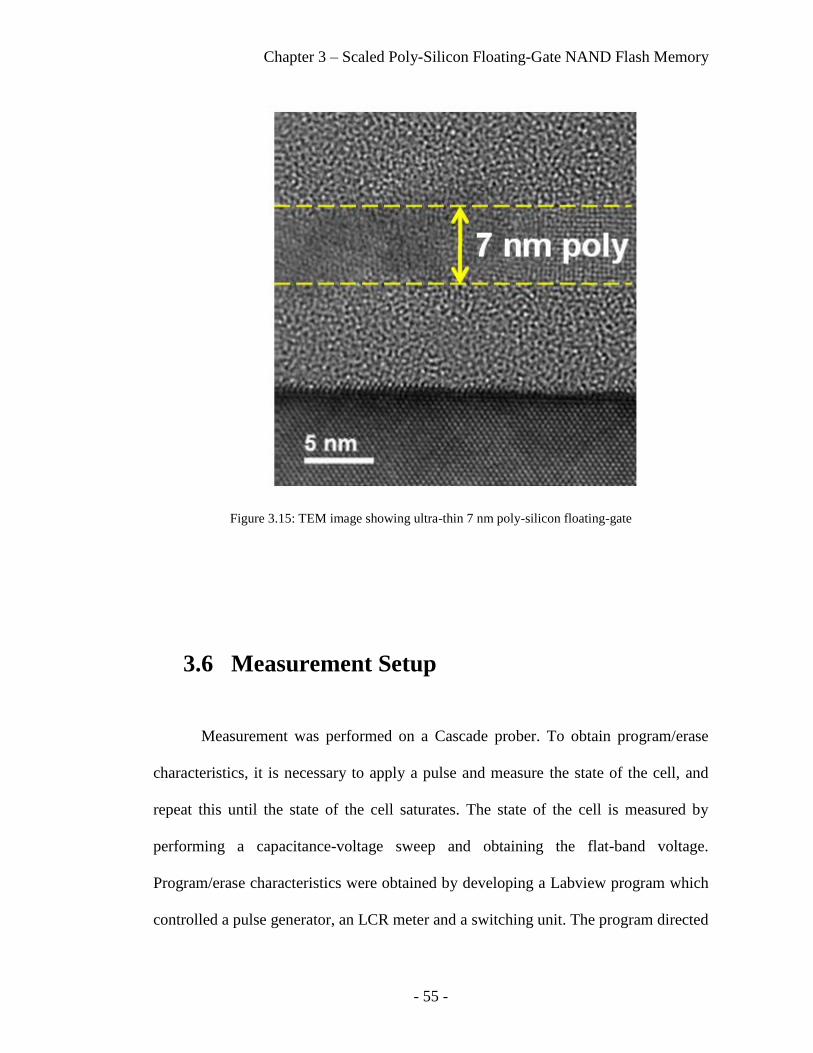
Chapter 3 – Scaled Poly-Silicon Floating-Gate NAND Flash Memory
- 55 -
Figure 3.15: TEM image showing ultra-thin 7 nm poly-silicon floating-gate
3.6 Measurement Setup
Measurement was performed on a Cascade prober. To obtain program/erase
characteristics, it is necessary to apply a pulse and measure the state of the cell, and
repeat this until the state of the cell saturates. The state of the cell is measured by
performing a capacitance-voltage sweep and obtaining the flat-band voltage.
Program/erase characteristics were obtained by developing a Labview program which
controlled a pulse generator, an LCR meter and a switching unit. The program directed

Chapter 3 – Scaled Poly-Silicon Floating-Gate NAND Flash Memory
- 56 -
the pulse generator to send a pulse, and then directed the switching unit to switch
connections to the LCR meter. The LCR meter performed a capacitance-voltage
sweep to obtain the flat-band voltage. The program then directed the switching unit to
switch back to the pulse generator, and the process of pulse-switch-measure-switch is
repeated until the flat-band voltage saturates. Similar Labview routines were
developed to measure retention and endurance.
3.7 Program/Erase characteristics
The program/erase characteristics of the floating-gate devices are discussed in
this section. The programming characteristics of 75 nm thick n-type poly-silicon
floating-gate devices are shown in figure 3.16. As mentioned before, the measurement
is performed by first applying a pulse, say, at 10 V (control-gate), followed by the
measurement of the flat-band voltage followed by a pulse at 10.5 V, then a
measurement and so on.

Chapter 3 – Scaled Poly-Silicon Floating-Gate NAND Flash Memory
- 57 -
Figure 3.16: Programming characteristics of 75 nm thick n-type poly-silicon floating-gate
The flat-band voltage keeps increasing with programming voltage until it
saturates. The voltage at which it saturates is called the saturation threshold voltage or
VT,SAT. It can be noted from the figure that the saturation voltage is quite large, ~ 8 V.
Figure 3.17 shows the erasing characteristics of 75 nm thick n-type poly-silicon
floating-gate. Here, again we note that the saturation voltage is quite large, ~ -8 V.
Therefore, the window of operation is large.

Chapter 3 – Scaled Poly-Silicon Floating-Gate NAND Flash Memory
- 58 -
Figure 3.17 : Erasing characteristics of 75 nm n-type poly-silicon floating-gate
The next important thing to note from figures 3.16 and 3.17 is that the slope of
the program/erase characteristics is exactly 1 until close to saturation. This is
indicative of a high quality device where the dielectrics are not leaky or trappy. If the
dielectrics are excessively leaky or trappy, the slope would be lesser than 1.
The reason for why the slope is 1 is described here. Following the development
in [3.20], this is based on the following two assumptions: a) the tunox current iG
increases with increasing floating-gate potential VFG (this is true for F-N tunneling
current in the normal range of operation); b) the floating gate potential VFG, which
controls electron injection, depends on control gate potential VCG and threshold

Chapter 3 – Scaled Poly-Silicon Floating-Gate NAND Flash Memory
- 59 -
voltage/flat-band voltage VT only through their difference VCG - VT (also true, shown
below)
Ignoring source, drain and body couplings,
VFG = GCR * VCG – ( Q / CTOT)
= GCR * VCG – (CIPD * VT / CTOT) because Q = CIPD * VT
= GCR * (VCG – VT) because GCR = CIPD / CTOT
Where
Q = Charge on FG
CTOT = Total FG capacitance
CIPD = IPD capacitance
Based on the two assumptions, we have iG = f ( VCG – VT )
Also, iG = -dQ/dt = CIPD * dVT/dt
Leading to dVT/dt = f ( VCG – VT ) / CIPD
If the starting value of VCG is low, f (VCG – VT) would be low, thereby the
change in VT would be low. The next VCG is higher by one step, say 0.5 or 1 V. Since
the VT only increases by a small amount, the new VCG – VT is higher than the last
time, therefore f (VCG – VT) is higher which implies that the change in VT is higher. If
the change in VT is still not as high as one VCG step, then the value of VCG – VT
increases further during the next step, and consequently does the change in VT. So the
Chapter 3 – Scaled Poly-Silicon Floating-Gate NAND Flash Memory
- 60 -
change in VT keeps increasing until it reaches the point when the change in VT is equal
to the VCG step. At this point, VCG - VT is constant, and continues to remain constant.
A similar argument can be made for a high starting value of VCG. The nature of the
function f(VCG-VT) determines the speed at which the sequence converges.
Therefore, this explains the nature of the presented program/erase
characteristics. Figures 3.16 and 3.17 also show program/erase characteristics for
different pulse widths. The longest pulse width starts programming at the smallest
voltage, and the curves for different pulse widths are shifted from each other by
approximately the same shift amount for each order of magnitude in pulse-width. The
same phenomenon is also seen in erase characteristics.
Figures 3.18 and 3.19 present the comparison of programming and erasing
characteristics for n-type poly-silicon FG of thicknesses 75 nm, 11 nm and 7 nm. It is
noted that all three have excellent saturation voltages and window, and the right slope
of 1. (These characteristics are for 100 ms pulse widths.) In general, the program/erase
characteristics are well-matched to one another when scaled from 75 nm thick n+ poly
silicon to ultra-thin 7 nm.

Chapter 3 – Scaled Poly-Silicon Floating-Gate NAND Flash Memory
- 61 -
Figure 3.18: Programming characteristics for various thicknesses of n-type poly-silicon FG devices
Figure 3.19: Erasing characteristics for various thicknesses of n-type poly-silicon FG devices
0
2
4
6
8
10
8 10 12 14 16 18 20
VFB
(V)
VPROG (V)
7 nm poly-Si
11 nm poly-Si
75 nm poly-Si

Chapter 3 – Scaled Poly-Silicon Floating-Gate NAND Flash Memory
- 62 -
3.8 Retention
The retention of these n+ poly-silicon floating-gate devices is tested at a
benchmark of 24 hours at 150 °C. The measurement is performed by programming a
number of devices to various flat-band voltages, performing the 24 hour 150 °C bake
and then measuring the threshold voltages of all the programmed cells. The retention
is plotted in figure 3.20 as loss in the flat-band voltage versus the starting (pre-bake)
flat-band voltage. From the figure, the retention is very good, as only less than 0.2 V is
lost for 5 V starting flat-band voltage, and the retention appears well-matched between
the poly-silicon FG devices of various thicknesses.
Figure 3.20: Retention for n-type poly-Si FG devices of various thicknesses

Chapter 3 – Scaled Poly-Silicon Floating-Gate NAND Flash Memory
- 63 -
So far, the poly-silicon devices seem to perform well with scaling in floating-
gate thickness. However, there are new problems that arise when scaling to ultra-thin
poly-silicon FG. The endurance of these devices will be discussed in the next chapter
when problems in scaling of poly-silicon FG devices are demonstrated.

Chapter 3 – Scaled Poly-Silicon Floating-Gate NAND Flash Memory
- 64 -
References
[3.1] Masuoka, F., Momodomi, M., Iwata, Y., Shirota, R., “New ultra high
density EPROM and flash EEPROM with NAND structure cell”, IEDM Tech. Digest,
1987.
[3.2] Barbara De Salvo, “Silicon non-volatile memories: paths of innovation”,
ISTE John Wiley 2009.
[3.3] P. Cappelletti, C. Golla, P. Olivo, and E. Zanoni, “Flash Memories”,
Kluwer Academic Publishers, MA, 1999.
[3.4] A.Fazio (Intel), “Challenges in charge based flash memory & phase
change memory”, EE310 Seminar, Stanford University, January 2007.
[3.5] International Technology Roadmap for Semiconductors: Process
Integration, Devices and Structures, 2009 edition.
[3.6] K. Ino “Scaling Challenges in NAND Flash Memory,” IEEE Silicon
Valley Chapter, New Frontiers in Memory Symposium, San Jose, CA, September 20,
2007.
[3.7] Dong-Chan Kim, et al., “A 2 Gb NAND flash memory with 0.044 μm2
cell size using 90 nm flash technology”, IEDM 2002.
[3.8] A. Fazio “Future Directions for Non-Volatile Memories,” IEEE Silicon
Valley Chapter, New Frontiers in Memory Symposium, San Jose, CA, September 20,
2007.
[3.9] K. Prall, “Scaling Non-volatile memory below 30 nm”, NVSMW 2007.

Chapter 3 – Scaled Poly-Silicon Floating-Gate NAND Flash Memory
- 65 -
[3.10] Jong-Ho Park et.al. (Samsung), “8 Gb MLC (multi-level cell) NAND
flash memory using 63 nm process technology”, IEDM 2004.
[3.11] F.Arai, pp.292-293, SSDM 2006.
[3.12] A.Fazio, "Future Directions of Non-Volatile Memory in Compute
Applications", IEDM 2009.
[3.13] K.Kim, J.Choi, “Future Outlook of NAND Flash Technology for 40nm
Node and Beyond “, pp 9-11, NVSMW 2006.
[3.14] Govoreanu et. al, " Scaling down the interpoly dielectric for next
generation Flash memory: Challenges and opportunities”, Solid-state electronics,
Vol.49, Iss.11, Nov 2005
[3.15] J.D.Lee, S.H.Hur and J.L.Choi, "Effects of Floating-Gate Interference
on NAND Flash Memory Cell Operation", IEEE Electron Device Letters, p.264,
Vol.23, Issue 5, May 2002.
[3.16] K.Kim, “Technology for sub-50nm DRAM and NAND flash
manufacturing “, IEDM 2005.
[3.17] J. De Vos et.al., European Solid-State Device Research Conference
(ESSDERC) 2008.
[3.18] Ted Kamins, "Polycrystalline silicon for integrated circuits and
displays", Kluwer academic publishers 1998.
[3.19] Shyam Raghunathan, Tejas Krishnamohan, Krishna Parat and Krishna
Saraswat, “Investigation of Ballistic Current in Scaled Floating-gate NAND Flash and
a Solution”, Proceedings of the Internation Electron Devices Meeting 2009.

Chapter 3 – Scaled Poly-Silicon Floating-Gate NAND Flash Memory
- 66 -
[3.20] C.Calligaro, A.Manstretta, A.Modelli and G.Corelli, "Technological and
Design Constraints for Multilevel Flash Memories", ICECS '96.

Chapter 4 – Scaled Poly-Silicon Floating-Gate: Problems to Ultimate Limit
- 67 -
Chapter 4
Scaled Poly-Silicon Floating-Gate:
Problems to Ultimate Limit
4.1 Introduction
A new reliability concern, arising from the programming current increasingly
going ballistically through the ultra-thin floating-gate, is described here. A new test
structure is built to experimentally investigate this effect. Experimental results
quantitatively show the magnitude of the effect. The implication of this effect is
observed by means of endurance data, which show thinner floating-gate devices
degrading faster. This reliability concern poses a major scaling challenge. Following
the discussion of this problem, other issues due to doping in ultra-thin poly-silicon
floating-gates are also discussed.

Chapter 4 – Scaled Poly-Silicon Floating-Gate: Problems to Ultimate Limit
- 68 -
4.2 The Ballistic Problem
4.2.1 Ballistic transport
Ballistic transport refers to carriers traversing a region without scattering [4.1-
4.6]. In general, carriers get scattered by phonons (lattice vibrations), dopant atoms,
other carriers etc. when traversing through a region. When the mean free path (average
distance between two scattering events) of the carrier is larger than the distance of the
region being traversed, there is a significant chance that the carrier will not face any
scattering event.
There are two kinds of scattering events: elastic and inelastic. Elastic scattering
refers to scattering events which do not involve change in energy of the carrier, but
only a change in momentum. Inelastic scattering refers to change in energy of the
carrier as a result of the scattering event.
Ballistic transport in Si/SiO2 stacks has been observed by Murota and co-
workers [4.7] using porous silicon. Figure 4.1 shows the schematic band diagram of
their study. Electrons are injected through Si/SiO2/Si/SiO2… layers of interconnected
nanocrystallites in porous silicon at a high electric field and the energy distribution of
the arriving electrons is measured. The energy distribution is shown on the right-side
of the figure. From the energy distribution, it can be clearly seen that the electrons
have not suffered many inelastic (energy-reducing) scattering events, and the energy
distribution is well-above expected levels for electrons in thermal equilibrium. In fact,
at 100K, the electrons seem to have experienced no inelastic scattering events at all.

Chapter 4 – Scaled Poly-Silicon Floating-Gate: Problems to Ultimate Limit
- 69 -
Figure 4.1 : Schematic band diagram of ballistic transport and emission via multiple tunneling through
interconnected nanocrystallites in porous silicon under a high electric field. [4.7]
4.2.2 Ballistic transport during programming
Figure 4.2 shows a band diagram describing ballistic transport during
programming.

Chapter 4 – Scaled Poly-Silicon Floating-Gate: Problems to Ultimate Limit
- 70 -
Figure 4.2: Band diagram describing ballistic transport during programming.
During programming, the electrons are injected into the floating-gate from the
substrate through F-N tunneling. Normally, these electrons get scattered and reach
thermal equilibrium in the floating-gate. Depending on the field across the IPD, a
small fraction of these scattered electrons will tunnel through the IPD to the control-
gate.
However, if the floating-gate is made thinner and thinner, some of the injected
electrons will not have sufficient scattering in the floating-gate. These „ballistic‟
electrons will traverse the IPD at high energy, posing a major reliability risk for the
IPD [4.8, 4.9]. Note that the electron does not have to be completely ballistic (zero
inelastic scattering events) in the FG for it to traverse the IPD at high energy. „Quasi-

Chapter 4 – Scaled Poly-Silicon Floating-Gate: Problems to Ultimate Limit
- 71 -
ballistic‟ electrons, which only lose a small amount of energy in the FG, may still have
enough energy to traverse the IPD energy barrier at sufficiently high energy.
The upcoming sections will explore the magnitude of this effect
experimentally. This issue is expected to become exponentially worse as the FG is
thinned down.
4.2.3 Test Structure
The test structure used for studying this issue is shown in Figure 4.3.
Figure 4.3 : Test Structure used to study ballistic transport

Chapter 4 – Scaled Poly-Silicon Floating-Gate: Problems to Ultimate Limit
- 72 -
This structure starts out with similar structure as described in figure 3.13. The
substrate, tunnel oxide, floating-gate, IPD and control-gate are described before. The
control-gate used here is n+ poly-silicon (~80 nm). A range of different active areas is
used as before. Following the patterning of the control-gate, two additional processing
steps are performed with the aim of introducing a contact to the floating-gate. The idea
behind introducing a floating-gate contact is that electrons scattered in the floating-
gate will be collected away by this contact, while the ballistic (and quasi-ballistic)
electrons will traverse across the IPD, and be collected at the control-gate.
To achieve the floating-gate contact, back-end low temperature silicon oxide
(LTO) is deposited on top of the patterned control-gate. Contact holes are etched in the
LTO to terminate on the control-gate and floating-gate. This is a very difficult step in
the fabrication of these structures, because the floating-gate is only a few nm thick and
it is easy to etch through it.
The contact hole etch was performed as follows: A well-characterized and
reproducible CHF3/O2 plasma dry etch was utilized to etch 80-90% of the LTO.
Following this dry etch, the photoresist was stripped and the remaining part was wet-
etched by a solution of 50:1 HF (with added surfactant). Buffered oxide etch (BOE)
was found to etch highly doped n-type poly-silicon relatively fast, hence HF was
utilized for the wet etch. Since HF has a problem with penetrating into smaller holes, a
surfactant was added to the HF. This combination of etches worked to achieve the
contact holes to the floating-gate and control-gate as desired.
Following the contact hole etch, aluminum was deposited as the metallization
layer and patterned to provide contacts to the floating-gate and control-gate.

Chapter 4 – Scaled Poly-Silicon Floating-Gate: Problems to Ultimate Limit
- 73 -
4.2.4 Measurement
The measurement of ballistic current using the structure shown in figure 4.3 is
described here. There are three terminals in the structure – the control-gate, the
floating-gate and the substrate. The substrate is grounded. The control-gate is fixed at
a sufficiently large programming bias, say, 20 V. The measurement is performed by
sweeping the floating-gate voltage from 0 in the positive (programming) direction.
The currents from all three terminals are measured.
Figure 4.4 shows the band diagram of the structure at the beginning of
measurement. As shown in the figure, the field across the tunnel oxide is very small at
the beginning, because the substrate is grounded and the floating-gate is at low bias.
The field across the IPD is very large at the beginning, as the control gate is fixed at
20 V, with the floating-gate at low bias. Figure 4.5 shows a schematic plot of the IPD
leakage current versus the floating-gate bias. As the figure shows, the IPD leakage
current first starts at a high magnitude due to the large IPD field. As the floating-gate
bias increases, the field across the IPD reduces, and this IPD leakage current falls
exponentially. The IPD leakage current flows between the floating-gate and the
control-gate. At low FG bias, there is negligible tunnel oxide current because of the
small field across the tunnel oxide.

Chapter 4 – Scaled Poly-Silicon Floating-Gate: Problems to Ultimate Limit
- 74 -
Figure 4.4: Band diagram during measurement at low FG bias. Substrate is grounded and CG is fixed at
20 V.
Figure 4.5: Shows the IPD leakage current at the start of measurement.

Chapter 4 – Scaled Poly-Silicon Floating-Gate: Problems to Ultimate Limit
- 75 -
Figure 4.6: Band diagram of measurement at high FG bias.
Figure 4.7: Shows schematics of expected currents at mid-to-high floating-gate bias.

Chapter 4 – Scaled Poly-Silicon Floating-Gate: Problems to Ultimate Limit
- 76 -
As the floating-gate bias is increased further (figure 4.6), the electric field
across the tunnel oxide increases, while the electric field across the IPD decreases. At
these low electric fields across the IPD, the IPD leakage is negligible. As the tunnel
oxide field increases, the tunneling current starts flowing from the substrate across the
tunnel oxide. Most of the tunneling carriers will be scattered and thermalized in the
floating-gate, and these electrons will be picked up at the floating-gate contact. A
fraction of the tunneling carriers will not be inelastically scattered in the floating-gate,
and these ballistic (or quasi-ballistic) electrons will be picked up at the control-gate.
As shown in figure 4.7, the tunnel oxide current from the substrate increases
exponentially with floating-gate bias. A fraction of that tunnel oxide current goes
ballistic from the substrate to the control-gate through the IPD, thus undetected by the
floating-gate contact.
Figures 4.5 and 4.7 are combined in figure 4.8 for the full range of
measurement. As the floating-gate bias increases, the IPD leakage decreases
exponentially and dies down. Beyond a certain floating-gate bias, the tunnel oxide
current begins from the substrate. The inelastically scattered electrons comprising the
tunnel oxide current, flow into the floating-gate contact. The ballistic current, a
fraction of the tunnel oxide current comprising the ballistic (and quasi-ballistic)
electrons, starts flowing into the control gate across the IPD. Thus, the measurement
of the control gate current would reveal a decreasing IPD leakage first, followed by an
increasing ballistic current. This measurement is applied to quantify the magnitude to
which carriers are ballistic in poly-silicon floating-gates.

Chapter 4 – Scaled Poly-Silicon Floating-Gate: Problems to Ultimate Limit
- 77 -
Figure 4.8: Schematic of expected currents during the ballistic current measurement technique
described.
4.2.5 Results
The measurement structure was fabricated with a range of poly-silicon
floating-gate thicknesses, going from 7 to 75 nm. The above-described measurements
were performed for these structures, and the results are summarized here. Figure 4.9
shows the results of the measurement performed on a 75 nm thick poly-silicon
floating-gate structure.

Chapter 4 – Scaled Poly-Silicon Floating-Gate: Problems to Ultimate Limit
- 78 -
Figure 4.9: Ballistic measurement data: 75 nm n-type poly-silicon floating-gate
The control gate current (ICG) decreases as the floating-gate bias is increased,
corresponding to the IPD leakage falling. As the floating-gate bias continues to
increase, the tunnel oxide current starts increasing. However, no concurrent increase
suggesting the ballistic component of tunnel oxide current, is observed in control gate
current. Hence, there is no ballistic component in the 75 nm thick poly-silicon
floating-gate device.
1E-14
1E-12
1E-10
1E-08
1E-06
1E-04
0 1 2 3 4 5 6 7 8 9 10
Cu
rre
nt
(A)
VFG (V)
ICG
ITUNOX
No Ballistic Component
75 nm Poly-Si FG

Chapter 4 – Scaled Poly-Silicon Floating-Gate: Problems to Ultimate Limit
- 79 -
Figure 4.10: Ballistic component measurement data in 30 nm n+ poly-silicon floating-gate device
Figure 4.10 shows the ballistic current measurement data in a device with 30
nm poly-silicon floating-gate. Here again, the control-gate current initially decreases
as the floating-gate bias is increased, eventually falling to very small levels. As the
floating-gate bias continues to increase, the tunnel oxide current starts increasing.
Now, a concurrent increase in the control-gate current is observed. As explained, this
control-gate current is present as a result of tunnel oxide current carriers travelling
ballistic through the floating-gate, collecting at the control-gate. From the data, it is
1E-14
1E-12
1E-10
1E-08
1E-06
1E-04
0 1 2 3 4 5 6 7 8 9 10
Cu
rre
nt
(A)
VFG (V)
ICG
ITUNOX
Ballistic
component (0.01% of ITUNOX)
30 nm Poly-Si FG

Chapter 4 – Scaled Poly-Silicon Floating-Gate: Problems to Ultimate Limit
- 80 -
observed that this ballistic component is about 0.01% of the tunnel oxide current, for
the 30 nm poly-silicon floating-gate sample.
Figure 4.11: Ballistic component measurement data for 10 nm n+ poly-silicon floating-gate sample
Figure 4.11 shows the ballistic component measurement data for a 10 nm poly-
silicon floating-gate device. Similar to the 30 nm floating-gate sample data, the
presence of the ballistic component is noted. The ballistic component is measured to
be 1.6% of tunnel oxide current, which is quite significant. It is also noted that the
ballistic component has shown an exponential increase from 0.01% at 30 nm floating-
1E-14
1E-12
1E-10
1E-08
1E-06
1E-04
0 1 2 3 4 5 6 7 8 9 10
Cu
rre
nt
(A)
VFG (V)
ICG
ITUNOX
Ballistic component (1.6% of ITUNOX)
10 nm Poly-Si FG

Chapter 4 – Scaled Poly-Silicon Floating-Gate: Problems to Ultimate Limit
- 81 -
gate to 1.6% at 10 nm floating-gate thickness, thereby underscoring the seriousness of
the problem as the floating-gate thickness is scaled down further.
4.2.6 Verification
In order to verify that the measured „ballistic‟ component has indeed originated
from the substrate tunnel oxide current, and is not any kind of IPD leakage current,
another experiment was performed. In this experiment, the measurement was
performed on structures with different active areas but same control-gate area, as
shown in figure 4.12. The figure shows two structures with the same gate stack but
different active areas (the tunnel oxide region). This means that the tunnel oxide area
through which the tunnel oxide current flows is different for the two structures, but the
IPD area (the area between floating-gate and control-gate) through which the IPD
leakage current flows is the same for the two structures.
Figure 4.13 shows the ballistic component measurement data for 11 nm poly-
silicon floating-gate using structures with different active areas. The result shows the
initial control-gate current, which is the IPD leakage current, remains the same for the
structures with different active areas. This is expected because the area of the IPD
region, which determines the IPD leakage current, remains the same. The tunnel oxide
current shown, scales proportional to the active region areas for the different
structures, as expected. The ballistic component of the control-gate current also scales
proportional to the active region areas. This proves that the origin of the ballistic
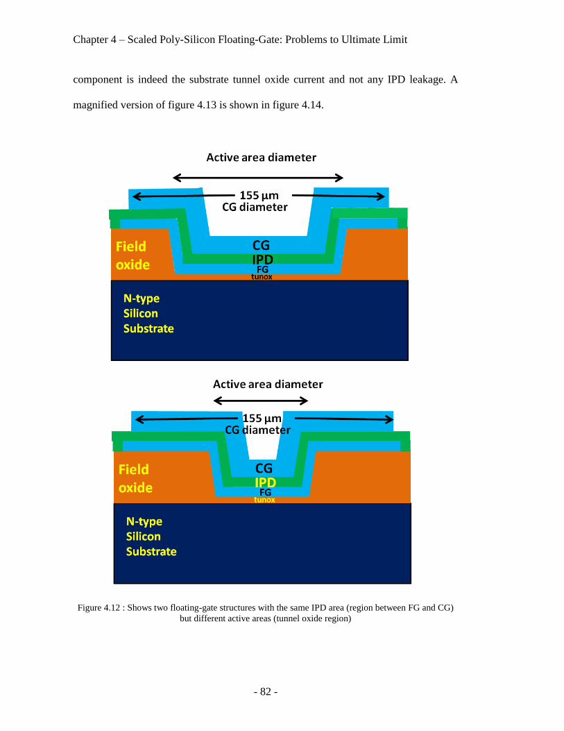
Chapter 4 – Scaled Poly-Silicon Floating-Gate: Problems to Ultimate Limit
- 82 -
component is indeed the substrate tunnel oxide current and not any IPD leakage. A
magnified version of figure 4.13 is shown in figure 4.14.
Figure 4.12 : Shows two floating-gate structures with the same IPD area (region between FG and CG)
but different active areas (tunnel oxide region)

Chapter 4 – Scaled Poly-Silicon Floating-Gate: Problems to Ultimate Limit
- 83 -
Figure 4.13: Ballistic component measurement data on 11 nm poly-silicon floating-gate sample for
structures with different active areas.
Figure 4.14: Magnified version of figure 4.13
5.E-13
5.E-12
5.E-11
5.E-10
5.E-09
5.E-08
5.E-07
5.E-06
5.E-05
0 1 2 3 4 5 6 7 8
Cu
rre
nt
(A)
VFG (V)
75 um55 um40 um
ICG same
for all 3 sizes
ITUNOX α
Areaactive
ICG αAreaactive
11 nm poly-Si FG
Active Area diameter
5.E-13
5.E-12
5.E-11
5.E-10
5.E-09
5.E-08
5.E-07
5 5.5 6 6.5 7
Cu
rre
nt
(A)
VFG (V)
ICG αAreaactive
ITUNOX α
Areaactive
11 nm poly-Si FG

Chapter 4 – Scaled Poly-Silicon Floating-Gate: Problems to Ultimate Limit
- 84 -
4.2.7 Mean Free Path
The ballistic component of tunnel oxide current is measured as described for
various n+ poly-silicon floating-gate thicknesses, and plotted in figure 4.15. The data
fits well on a straight line (note the vertical axis is on an exponential scale). Therefore,
a mean free path can be extracted by fitting to a simple exponential law equation.
Applying this, the mean free path is obtained as ~ 4 nm in n+ poly-silicon.
Note that this is an inelastic mean free path, because inelastic scattering events that
reduce energy of the carriers, are those that determine ballistic transport of the electron
through the floating-gate. (Elastic scattering events will have a second order influence,
because a carrier subject to more elastic scattering takes longer to traverse the region,
making it more likely to be inelastically scattered.)

Chapter 4 – Scaled Poly-Silicon Floating-Gate: Problems to Ultimate Limit
- 85 -
Figure 4.15: Inelastic mean free path extraction by slope of ballistic component versus floating-gate
thickness
4.2.8 Impact (Endurance)
The ballistic component of programming current has been demonstrated and
quantified so far. In this section, the impact of these ballistic carriers is discussed. This
is accomplished by performing endurance tests on floating-gate capacitors with
various poly-silicon floating-gate thicknesses ranging from 75 nm to 7 nm. The
endurance test involves repeated program/erase cycles. During programming, the
ballistic high-energy carriers that traverse the IPD pose a reliability threat to the IPD.
0.01
0.1
1
10
0 10 20 30
Pe
rce
nta
ge o
f B
allis
tic
curr
en
t
FG THICKNESS (nm)
Slope = -0.24
Mean Free Path in poly-Si =
1/0.24 = ~4 nm
Poly-Si FG
Percentage of Ballistic current =
100*IBALLISTIC / ITUNOX

Chapter 4 – Scaled Poly-Silicon Floating-Gate: Problems to Ultimate Limit
- 86 -
Repeated programming events lead to an accumulation of damage, which is expected
to be observed in these tests.
Figure 4.16 shows cycling data on 75 nm, 10 nm and 7 nm thick n+ poly-
silicon floating-gate devices. These devices are cycled at 14 V programming bias and -
14 V erasing bias for 100 ms, corresponding to flat-band voltages of ±5 V. The 75 nm
poly-silicon floating-gate device does not show much degradation, while the thinner
devices, especially the 7 nm poly-silicon floating-gate device shows much more
degradation, pointing to ballistic carriers causing reliability issues.
Figure 4.16: Cycling data (+- 14 V, 100 ms) on 75 nm, 10 nm and 7 nm poly-silicon floating-gate
devices. The 7 nm floating-gate devices show more degradation
-0.6
-0.4
-0.2
0
0.2
1 10 100 1,000 10,000
Ch
ange
in V
FB(V
)
Number of Cycles
7 nm poly-Si10 nm poly-Si75 nm poly-Si
VPROG = 14 V, 100 ms
-0.3
-0.1
0.1
0.3
0.5
0.7
1 10 100 1,000 10,000Ch
ange
in V
FB(V
)
Number of Cycles
VERASE = -14 V, 100 ms

Chapter 4 – Scaled Poly-Silicon Floating-Gate: Problems to Ultimate Limit
- 87 -
Figure 4.17 shows similar endurance testing performed on 75 nm and 10 nm
poly-silicon floating-gate devices programmed at 17 V for 100 µs and erased at -14 V
for 100 ms (corresponding ± 5 V flat-band voltages). Again, it is clearly observed that
the thinner poly-silicon floating-gate device degrades more. It is also worth noting that
programming at higher fields for shorter pulse times (for the same flat-band voltage)
degrades the device more.
Figure 4.17: Cycling data (+17 V, 100 µs and -14 V, 100 ms) on 75 nm and 10 nm poly-silicon
floating-gate devices. The 10 nm floating-gate devices show more degradation
-0.8
-0.6
-0.4
-0.2
0
0.2
1 10 100 1,000 10,000
Ch
ange
in V
FB(V
)
Number of Cycles
10 nm poly-Si
75 nm poly-Si
VPROG = 17 V, 100 µs
-0.2
0
0.2
0.4
1 10 100 1,000 10,000
Ch
ange
in V
FB(V
)
Number of Cycles
VERASE = -14 V, 100 ms

Chapter 4 – Scaled Poly-Silicon Floating-Gate: Problems to Ultimate Limit
- 88 -
Figure 4.18 shows the capacitance-voltage plots for devices subjected to the
endurance tests in figure 4.17. The capacitance-voltage plot of the 10 nm poly-silicon
floating-gate device shows a larger degradation in slope and more pronounced hump
compared to the 75 nm poly-silicon floating-gate device, indicating poorer dielectric
quality. The high energy ballistic electrons break bonds in the IPD, and create an
increasing number of traps over time, which are responsible for the degradation in the
capacitance-voltage curves.
Figure 4.18: Capacitance-Voltage curves of cycled devices indicating more degradation in the 10 nm
poly-silicon floating-gate device compared to the 75 nm floating-gate device.
1E-12
2E-12
3E-12
4E-12
5E-12
6E-12
7E-12
8E-12
-1.5 -1.0 -0.5 0.0 0.5 1.0 1.5
Cap
acit
ance
(F)
VCG (V)
Starting
10K cycles
Slope degrades by ~35%
75 nm poly-Si FG
1E-12
2E-12
3E-12
4E-12
5E-12
6E-12
7E-12
8E-12
-1.5 -1.0 -0.5 0.0 0.5 1.0 1.5
Cap
acit
ance
(F)
VCG (V)
Starting
10K cycles
Slope degrades by ~70%
10 nm poly-Si FG
Larger Hump

Chapter 4 – Scaled Poly-Silicon Floating-Gate: Problems to Ultimate Limit
- 89 -
4.2.9 Summary
In this section, a new reliability failure mechanism was introduced. As the
floating-gate is thinned down, the programming carriers start going increasingly
ballistic, and these high-energy carriers pose a reliability concern when they traverse
the IPD. A new measurement structure was built to measure this ballistic effect
experimentally. The experiments quantified the magnitude of this and extracted the
inelastic mean free path of electrons in poly-silicon. Finally, the impact of this was
shown by means of endurance tests on devices with various poly-silicon floating-gate
thicknesses, revealing that the thinnest floating-gate devices degraded the most.
4.3 Poly-silicon depletion
4.3.1 Poly depletion effect
This effect [4.13] is well known in CMOS technology. Consider figure 4.19. In
MOS transistors, high electric field due to a combination of higher supply voltage and
thinner gate oxide causes band bending even in a heavily doped poly-silicon gate. This
causes depletion in the poly-silicon gate. The effect of depletion is to increase the
effective oxide thickness and reduce the effective oxide capacitance.

Chapter 4 – Scaled Poly-Silicon Floating-Gate: Problems to Ultimate Limit
- 90 -
Figure 4.19: The poly-depletion effect. Due to the depletion in the poly-silicon gate, the effective oxide
thickness increases and the effective capacitance decreases. Source: [4.13]
tox(electrical)
tox(physical)
Gate depletion
OxideSubstrateGate

Chapter 4 – Scaled Poly-Silicon Floating-Gate: Problems to Ultimate Limit
- 91 -
4.3.2 Poly depletion in NAND flash memory
As observed in MOS transistor technology, poly-silicon depletion can also
occur in NAND flash memory devices. Consider figure 4.20.
Figure 4.20: Shows a plot of poly-silicon floating-gate doping versus technology node. Also shows an
increase in the IPD thickness variation due to poly-depletion with scaling. Source: [4.14]
The band diagram in the figure shows that there is an effective increase in the
EOT of the tunnel oxide and the IPD due to poly-depletion, which widens the
threshold voltage distribution. The variation gets worse with scaling, which is a
serious concern, given the small margins available for design.
Spessot and co-workers [4.15] demonstrate a decrease in the erase efficiency
as a result of depletion in the poly-silicon floating-gate (figure 4.21). From the band
diagram, it is observed that the floating-gate goes into deep-depletion near the IPD
side (due to lower doping on the IPD side in this particular experiment). The voltage

Chapter 4 – Scaled Poly-Silicon Floating-Gate: Problems to Ultimate Limit
- 92 -
drop across the depletion region, leads to a smaller voltage drop and electric field
across the tunnel oxide. In other words, the additional capacitance caused by the
depletion reduces the effective GCR of the device, which leads to a smaller field
across the tunnel oxide. As a result of the smaller tunnel oxide field, the erase is
slower.
Figure 4.21: As a result of the poly-depletion, there is a decreased field across the tunnel oxide which
makes the erase slower. Source: [4.15]

Chapter 4 – Scaled Poly-Silicon Floating-Gate: Problems to Ultimate Limit
- 93 -
4.3.3 Experiment
The test structure used was a floating-gate capacitor like the one described in
figure 3.13. Figure 4.22 shows the capacitance-voltage plots for 20 nm, 12 nm and 7
nm thick poly-silicon floating-gate devices.
Figure 4.22: Shows the capacitance-voltage plots for poly-silicon floating-gate devices. The 7 nm
device shows a characteristic poly-depletion dip in the capacitance.
It can be observed that the 7 nm device shows the characteristic poly-depletion
dip in the capacitance. This occurs as a result of the ultra-thin poly-silicon floating-
gate getting fully depleted. The ultra-thin 7 nm layer may also have lower doping
density, contributing to easier depletion, because phosphorus tends to segregate into
grain boundaries [4.16, 4.17] during slow cooling after the high temperature anneal.
0
0.2
0.4
0.6
0.8
1
-5 0 5 10
No
rmal
ize
d
Cap
acit
ance
VCG (V)
20 nm FG
12 nm FG
7 nm FG

Chapter 4 – Scaled Poly-Silicon Floating-Gate: Problems to Ultimate Limit
- 94 -
The grains are smaller at the bottom of a poly-silicon layer, therefore a thinner poly-
silicon layer tends to have a higher proportion of grain boundaries, which can lead to
more segregation of phosphorus. (Note that this segregation could be avoided by rapid
cooling.) The sheet resistances were – 130 Ω/sq for 70 nm poly-silicon versus ~10,000
Ω/sq for 7 nm poly-silicon, also suggesting lower doping density in the ultra-thin
layer. (Note that a direct extraction of doping cannot be performed from the sheet
resistance, because the ultra-thin layer may have decreased mobility due to grain
boundary and surface scattering.)
It is possible to amplify the effect of poly-depletion, and observe it more easily
by using an emulated wrap structure (larger area between control-gate and floating-
gate) like the one in figure 3.13. The data in figure 4.22 is for an emulated wrap of ~2.
Figure 4.23 shows the effect of wrap by displaying capacitance-voltage plots for
various levels of wrap. It can be clearly observed that the effect is much more
pronounced for larger wraps. This is explained by figure 4.24. This figure shows the
Medici simulated potential contours for an emulated wrap structure. In this figure, the
area between the floating-gate and control-gate is larger than the tunnel oxide area.
(The substrate is STI isolated). The first plot is for an undepleted floating-gate device.
In this device, the control-gate couples perfectly to the floating-gate over its entire
area, and the floating-gate couples to the substrate, as is clear from the potential
contours. The second plot is for a depleted floating-gate device. The additional
capacitance due to the depleted floating-gate is shown. In this case, the potential
contours reveal that the control gate has to couple to the substrate directly, in the area
outside of the tunnel oxide stack region. This leads to a much larger decrease in the

Chapter 4 – Scaled Poly-Silicon Floating-Gate: Problems to Ultimate Limit
- 95 -
effective GCR as a result of poly-depletion, compared to the case without wrap,
thereby making the poly-depletion effect easier to observe.
Figure 4.23: The poly-depletion effect is much more pronounced for larger emulated wraps
0.0
0.2
0.4
0.6
0.8
1.0
-1 4 9 14
No
rmal
ize
d c
apac
itan
ce
Gate voltage (V)
Wrap 1
Wrap 2
Wrap 4
7 nm poly-silicon FG
0.0
0.2
0.4
0.6
0.8
1.0
-1 4 9 14
No
rmal
ize
d c
apac
itan
ce
Gate voltage (V)
Wrap 1
Wrap 2
Wrap 4
12 nm poly-silicon FG

Chapter 4 – Scaled Poly-Silicon Floating-Gate: Problems to Ultimate Limit
- 96 -
Figure 4.24: Medici simulation potential contours for depleted and undepleted FG. Shows effect of
emulated wrap in amplifying poly-depletion.
(1/CTOT) ~ (1/CIPD * ACG) + (1/Ctunox * Asubs)Ignoring fringe
Depleted
(1/CTOT) ~ (1/CIPD * Asubs) + (1/Ctunox * Asubs)+ (1/CPoly * Asubs) + CG Fringe
Undepleted
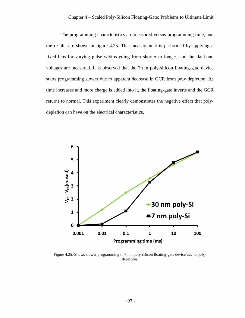
Chapter 4 – Scaled Poly-Silicon Floating-Gate: Problems to Ultimate Limit
- 97 -
The programming characteristics are measured versus programming time, and
the results are shown in figure 4.25. This measurement is performed by applying a
fixed bias for varying pulse widths going from shorter to longer, and the flat-band
voltages are measured. It is observed that the 7 nm poly-silicon floating-gate device
starts programming slower due to apparent decrease in GCR from poly-depletion. As
time increases and more charge is added into it, the floating-gate inverts and the GCR
returns to normal. This experiment clearly demonstrates the negative effect that poly-
depletion can have on the electrical characteristics.
Figure 4.25: Shows slower programming in 7 nm poly-silicon floating-gate device due to poly-
depletion.
0
1
2
3
4
5
6
0.001 0.01 0.1 1 10 100
VFB
-V
FB(e
rase
d)
Programming time (ms)
30 nm poly-Si
7 nm poly-Si

Chapter 4 – Scaled Poly-Silicon Floating-Gate: Problems to Ultimate Limit
- 98 -
4.3.4 Summary
The poly-depletion effect is proven to be a problem for scaled poly-silicon
floating-gate NAND flash memory devices, in addition to the ballistic carrier issue.
Other issues of poly-silicon floating-gate devices include poor compatibility with
high-k dielectrics and difficulty in depositing smooth layers with ultra-small
thicknesses. As a result of these problems, metals are explored as alternative materials
for the scaled floating-gate.

Chapter 4 – Scaled Poly-Silicon Floating-Gate: Problems to Ultimate Limit
- 99 -
References
[4.1] Lundstrom, "Fundamentals of Carrier Transport", Cambridge University
Press (2000).
[4.2] Hayes, J.R., Levi, A.F.J., Gossard, A.C., Hutchinson, A.L. and English,
J.H. "Base transport dynamics in a heterojunction bipolar transistor", Applied Physics
Letters, 49, 1481-3, 1986.
[4.3] Levi, A.F.J. and Yafet, Y. "Nonequilibrium electron transport in bipolar
devices", Applied Physics Letters, 51, 42-4, 1987.
[4.4] Hayes, J.R., Levi, A.F.J. and Weigmann, W. "Dynamics of electron
cooling in GaAs", Applied Physics Letters, 48, 1365-7, 1986.
[4.5] Capasso, F. (ed.) "Physics of quantum devices", Springer series in
electronics and photonics, Vol.28, Springer-Verlag, New York 1989.
[4.6] Datta, S. "Electronic transport in mesoscopic systems", Cambridge
University Press, Cambridge, UK, 1995.
[4.7] Kojima, Sheng and Koshida, MRS Symposium 2001.
[4.8] DiMaria, D. J. and Kerr, D. R. (1975) Interface effects and high
conductivity in oxides grown from polycrystalline silicon. Applied Physics Letters.
27, 505.
[4.9] S.Raghunathan, T.Krishnamohan, K.Parat and K.C.Saraswat,
“Investigation of Ballistic Current in Scaled Floating-Gate NAND Flash and a
Solution”, Proceedings of the Internation Electron Devices Meeting, December 2009.

Chapter 4 – Scaled Poly-Silicon Floating-Gate: Problems to Ultimate Limit
- 100 -
[4.10] J.D.Lee, S.H.Hur and J.L.Choi, "Effects of Floating-Gate Interference
on NAND Flash Memory Cell Operation", IEEE Electron Device Letters, p.264,
Vol.23, Issue 5, May 2002.
[4.11] Kinam Kim, “Technology for sub-50nm DRAM and NAND flash
manufacturing “, IEDM 2005.
[4.12] J. De Vos et.al., European Solid-State Device Research Conference
(ESSDERC) 2008.
[4.13] Buchanan and Lo, Proc. ECS Vol. PV 96-1, 1996
[4.14] Yohwan Koh, “NAND Flash Scaling beyond 20 nm”, pg.3-5,
International Memory Workshop 2009.
[4.15] A.Spessot, C.M.Compagnoni, F.Farina, A.Calderoni, A.Spinelli and
P.Fantini, "Effect of Floating-Gate Polysilicon Depletion on theErase Efficiency of
NAND Flash Memories", IEEE Electron device letters, vol.31, no.7, July 2010.
[4.16] Ted Kamins, "Polycrystalline Silicon for Integrated Circuits and
Displays", Kluwer academic publishers (1998).
[4.17] M M Mandurah, K.C.Saraswat, C.R.Helms and T.I.Kamins, "Dopant
segregation in polycrystalline silicon", J. Appl. Phys. 51, 5755-5763 (November
1980).
Chapter 5 – Metal Floating-Gate
- 101 -
Chapter 5
Metal Floating-Gate
5.1 Introduction
The scaling of poly-silicon floating-gate has been studied in detail so far,
revealing serious challenges. In this chapter, the use of a metal floating-gate as a
possible replacement for poly-silicon is explored. The metal floating-gate is
experimentally demonstrated to provide excellent electrical performance. The metal
floating-gate is also demonstrated to solve the ballistic carrier and poly-depletion
issues discussed in chapter 4. The factors underlying the choice of metal are discussed
in detail. From the various options available, TiN (or TaN) is chosen as the preferred
floating-gate. The TiN floating-gate is scaled down to ultra-thin 3 nm, which shows
excellent electrical performance at even such low thicknesses. Utilization of such an
ultra-thin floating-gate would greatly reduce cell-to-cell interference.

Chapter 5 – Metal Floating-Gate
- 102 -
5.2 Metal Floating-Gate Device
Cell-to-cell interference [5.1-5.4] is a major problem in ultra-scaled NAND
flash memories. Scaling the thickness of the floating-gate [5.5-5.7] helps reduce the
coupling between adjacent cells and reduce interference. The scaling of poly-silicon
floating-gates was studied in detail in chapters 3 and 4. The serious issues of ballistic
transport of injected carriers in the ultra-scaled floating-gate, and poly-depletion
induced problems, were identified. In order to overcome these issues, the use of a
metal-based floating-gate is explored.
The structure used for studying these metal floating-gate devices is the
floating-gate capacitor structure as discussed before, and shown in figure 5.1.
Figure 5.1: Floating-gate capacitor structure used to study program/erase and reliability performance of
metal floating-gate devices.
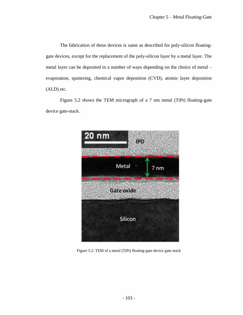
Chapter 5 – Metal Floating-Gate
- 103 -
The fabrication of these devices is same as described for poly-silicon floating-
gate devices, except for the replacement of the poly-silicon layer by a metal layer. The
metal layer can be deposited in a number of ways depending on the choice of metal –
evaporation, sputtering, chemical vapor deposition (CVD), atomic layer deposition
(ALD) etc.
Figure 5.2 shows the TEM micrograph of a 7 nm metal (TiPt) floating-gate
device gate-stack.
Figure 5.2: TEM of a metal (TiPt) floating-gate device gate-stack

Chapter 5 – Metal Floating-Gate
- 104 -
The program/erase characteristics of this device are shown in figures 5.3 and
5.4. As shown, these devices have excellent window in excess of 20 V, demonstrating
that metals are suitable for use as charge-storage electrodes in floating-gate memories.
Figure 5.3: Programming characteristics of TiPt floating-gate device
Figure 5.4: Erasing characteristics of TiPt floating-gate device
0
5
10
15
8 10 12 14 16 18 20 22 24 26 28
VFB
(V)
VPROG(V)
1 ms pulse100 ms pulse

Chapter 5 – Metal Floating-Gate
- 105 -
5.3 Ballistic Component in Metal Floating-Gates
In chapter 4, the problem of programming carriers going increasingly ballistic
[5.8] as the poly-silicon floating-gate is scaled down, was studied. Here, the ballistic
component in metal floating-gate devices is studied, as metal floating-gates are viewed
as a solution to this issue due to much higher levels of inelastic electron scattering
[5.9].
To study the ballistic component, the structure with floating-gate contact
described earlier and shown in figure 5.5 is used. As described before, tunnel oxide
carriers that get scattered and thermalized in the floating-gate, will be collected at the
floating-gate contact, while the ballistic (and quasi-ballistic) carriers will be collected
at the control-gate.
The measured data for the 7 nm TiPt floating-gate sample is shown in figure
5.6. The figure also shows a comparison with the 7 nm n+ poly-silicon floating-gate
sample data. The nature of the plot is the same as described before – initial decrease in
the IPD leakage current, followed by increase in the ballistic component concurrent
with the onset of tunnel oxide current. From the figure, it is clear that the ballistic
component is much lower (1000X) in the metal floating-gate device compared to the
poly-silicon floating-gate device. It is also worth noting that the IPD leakage of the
metal floating-gate device is lower than the n+ poly-silicon counterpart, due to the
deeper work-function of the metal used here. Therefore, the metal floating-gate is
found to be effective at reducing the ballistic carrier issue.
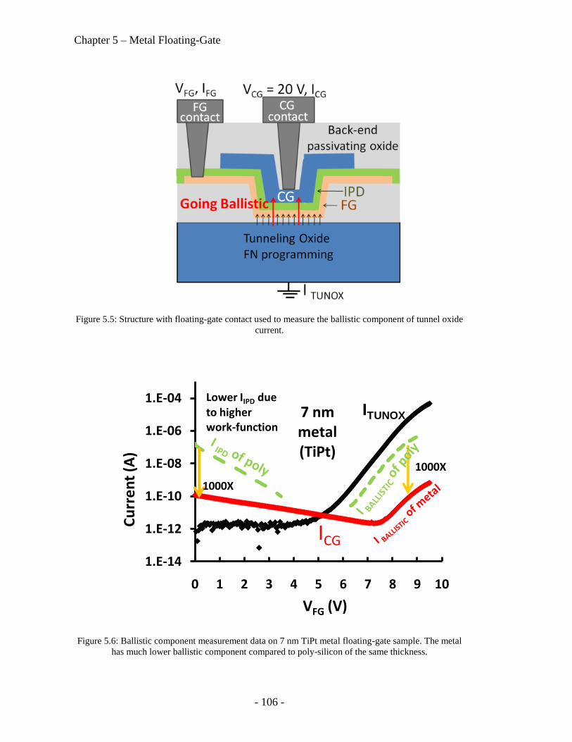
Chapter 5 – Metal Floating-Gate
- 106 -
Figure 5.5: Structure with floating-gate contact used to measure the ballistic component of tunnel oxide
current.
Figure 5.6: Ballistic component measurement data on 7 nm TiPt metal floating-gate sample. The metal
has much lower ballistic component compared to poly-silicon of the same thickness.
1.E-14
1.E-12
1.E-10
1.E-08
1.E-06
1.E-04
0 1 2 3 4 5 6 7 8 9 10
Cu
rre
nt
(A)
VFG (V)
ICG
ITUNOX7 nm metal (TiPt)
Lower IIPD due to higher work-function
1000X
1000X

Chapter 5 – Metal Floating-Gate
- 107 -
The ballistic component in some other metals was also studied using the
structure shown in figure 5.5. The results are summarized in figure 5.7.
Figure 5.7: Percentage of ballistic current plotted versus floating-gate thickness for a variety of
materials. In general, it can be observed that metals have lower ballistic component compared to poly-
silicon due to increased inelastic electron scattering.
It is clearly observed that the ballistic component is smaller in metals
compared to poly-silicon. Hence, use of a metal floating-gate would help to solve the
ballistic carrier issue.
It is also observed that there are differences in the level of ballistic current
between different metals. This is due to the differences in the level of inelastic
scattering between different metals. This is illustrated using figure 5.8.
0.00001
0.0001
0.001
0.01
0.1
1
10
0 5 10 15 20 25 30
Pe
rce
nta
ge o
f B
allis
tic
curr
en
t
FG THICKNESS (nm)
Poly-Si FG
Ti (2 nm) + Pt (5 nm)
Pt
Ti (5 nm) + Pt (2 nm)
TiN, W
Pt
Pt
Pt

Chapter 5 – Metal Floating-Gate
- 108 -
Figure 5.8: Shows the definition of work-function and Fermi energy in a metal. Also shows the density
of states (DOS) versus energy.
The level of scattering [5.10] in a material is directly related to the density of
states of the material at the energy of interest. The larger the density of states, the
higher is the level of scattering. Assuming a very simple parabolic model, the density
of states increases with energy as shown. Differences in the band structures of
different materials will also contribute to different density of states. Ignoring that for a
simple first-order comparison, the density of states (and the level of scattering) can be
compared by the energy of the electron above the conduction band of the material.
In metals, the Fermi-level is situated above the conduction band. The
difference in energy between the conduction band and the Fermi-level is called the
Fermi-energy. The difference in energy between the Fermi-level and the vacuum level
is called the work-function. To compare two metals for a given incoming electron, the
differences in both the Fermi energies and the work-functions have to be taken into
account, as is clear from figure 5.8.

Chapter 5 – Metal Floating-Gate
- 109 -
Taking Fe and Au for comparison, we can consider the work-functions and
Fermi energies shown in table 5.1.
Element Work-function Fermi energy
Li 2.93 4.74 Na 2.36 3.24 K 2.29 2.12 Rb 2.26 1.85 Cs 2.14 1.59 Cu 4.53-5.10 7.00 Ag 4.52-4.74 5.49 Au 5.1-5.47 5.53 Be 4.98 14.3 Mg 3.66 7.08 Ca 2.87 4.69 Sr 2.59 3.93 Ba 2.52-2.7 3.64 Nb 3.95-4.87 5.32 Fe 4.67-4.81 11.1 Mn 4.1 10.9 Zn 3.63-4.9 9.47 Cd 4.08 7.47 Hg 4.475 7.13 Al 4.06-4.26 11.7 Ga 4.32 10.4 In 4.09 8.63 Tl 3.84 8.15 Sn 4.42 10.2 Pb 4.25 9.47
Table 5.1: Work-functions and Fermi energies of some elements [5.11, 5.12]
The work-function of Fe is 4.7 compared to Au at 5.2. However, the Fermi
energy of Fe is 11 compared to Au at 5.5. Therefore, based on the simple model
discussed above, Fe is expected to scatter electrons more than Au. It should also be
remembered that the work-function and other surface properties of metals are strongly

Chapter 5 – Metal Floating-Gate
- 110 -
dependent on the surface morphology, orientation and other factors related to surface
preparation.
5.4 Absence of Poly-depletion effects
In chapter 4, it was observed that problems occur as a result of depletion in the
poly-silicon floating-gate. Since no doping is involved in metals, this effect is not
expected to be observed, and is confirmed through the experimental results shown in
figures 5.9 and 5.10.
Figure 5.9 shows the capacitance voltage plot of a 3 nm TiN floating-gate
sample. There is no characteristic poly-depletion dip in the capacitance. Figure 5.10
shows the flat-band voltage versus programming time for a fixed bias. There is no
initial slow period of programming as was observed in ultra-thin poly-silicon floating-
gate samples. The slower period of programming was due to the decreased GCR of the
device as the poly-silicon got depleted.
Hence, as expected, there are no doping-related issues observed in these metal
floating-gate samples.

Chapter 5 – Metal Floating-Gate
- 111 -
Figure 5.9: Capacitance-Voltage plot of 3 nm TiN FG capacitor showing no characteristic poly-
depletion dip in the capacitance.
Figure 5.10: Flat-band voltage versus programming time for 3 nm TiN FG sample. There is no slow-
down in the beginning as observed with depleted poly-silicon samples due to decreased GCR.
0
0.1
0.2
0.3
0.4
0.5
0.6
0.7
0.8
0.9
1
-4 -2 0 2 4 6 8
No
rmal
ize
d C
apac
itan
ce
VPROG(V)
0
1
2
3
4
5
6
0.001 0.01 0.1 1 10 100
VFB
-V
FB(e
rase
d)
Programming time (ms)
3 nm metal

Chapter 5 – Metal Floating-Gate
- 112 -
5.5 Metal floating-gate work-function
The work-function of the metal floating-gate has a significant impact on the
operation of the device. This is illustrated by figures 5.11 and 5.12.
Figure 5.11 shows band diagrams that explain why a deeper work-function FG
device erases slower than a shallower work-function FG device. The deeper work-
function FG device has a larger barrier height for F-N tunneling carriers out from the
FG through the tunnel oxide onto the substrate.
Figure 5.12 shows band diagrams for a deeper work-function FG device
having better retention compared to a shallower work-function FG device. This is
because the deeper work-function FG device stores the charge in a deeper potential
well (larger energy barriers).
Figure 5.13 shows experimental data confirming that a shallower work-
function floating-gate device (Ti+Pt) erases faster than a deeper work-function
floating-gate device (Pt).
Therefore, the metal work-function poses an important trade-off in the choice
of metals for the floating-gate. A deeper work-function metal will provide better
retention but will erase slower.

Chapter 5 – Metal Floating-Gate
- 113 -
Figure 5.11: Band diagrams showing that deeper work-function FG leads to slower erase. Top figure
shows shallower work-function FG device and bottom figure shows deeper work-function FG device.
Deeper work-function FG has larger barrier to tunneling out from FG to substrate.

Chapter 5 – Metal Floating-Gate
- 114 -
Figure 5.12: Band diagrams showing that deeper work-function FG leads to better retention. Top figure
shows shallower work-function FG device and bottom figure shows deeper work-function FG device.
Deeper work-function FG device stores charge in a deeper potential well.

Chapter 5 – Metal Floating-Gate
- 115 -
Figure 5.13: Shows deeper work-function (Pt) FG device erase slower than shallower work-function
(Ti+Pt) FG device
5.6 Choice of metal : TiN, TaN
Since the work-function of the metal essentially determines a trade-off
between erase-speed and retention, a mid-gap material such as TiN or TaN is picked
as the floating-gate of choice. The following summarizes the reasons for picking
TiN/TaN as the preferred floating-gate.
Mid-gap material: Good trade-off between erase-speed and retention
From figure 5.7, it is observed that TiN has a very small ballistic
component.
-4.5
-4
-3.5
-3
-2.5
-2
-1.5
-1
-0.5
0
-16 -14 -12 -10
Flat
-ban
d v
olt
age
(V)
Erase Voltage (V)
Ti (5 nm) + Pt (10 nm)
Pt (10 nm)

Chapter 5 – Metal Floating-Gate
- 116 -
Ease of processing: TiN/TaN are already used in standard CMOS
processing.
Thermal stability: TiN/TaN have shown high thermal stability (upto
1000 C) and compatibility with dielectrics. [5.13]
5.7 Ultra-thin 3 nm TiN floating-gate device
Based upon the reasons elaborated in section 5.6, TiN has been chosen as the
floating-gate, and scaled down to ultra-thin 3 nm. The results are presented in this
section.
Figures 5.14 and 5.15 show the programming and erasing characteristics of the
3 nm TiN floating-gate device. It can be observed that an excellent window of ~20 V
is obtained with a perfect slope of 1 for the program/erase characteristics.
Figure 5.16 shows retention data for the 3 nm TiN floating-gate sample. As
discussed before, the retention is characterized by programming devices to various
levels and baking them at 150 C for 24 hours. It can be observed that the retention is
quite good as expected for a mid-gap work-function material.
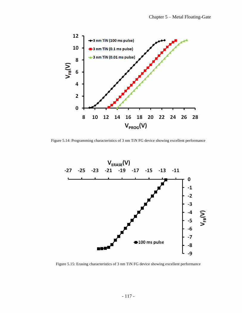
Chapter 5 – Metal Floating-Gate
- 117 -
Figure 5.14: Programming characteristics of 3 nm TiN FG device showing excellent performance
Figure 5.15: Erasing characteristics of 3 nm TiN FG device showing excellent performance

Chapter 5 – Metal Floating-Gate
- 118 -
Figure 5.16: Retention data for 3 nm TiN floating-gate device
5.8 Summary
In this chapter, the use of a metal floating-gate as a replacement for poly-
silicon was explored. The metal floating-gate was demonstrated to solve the ballistic
carrier and poly-depletion issues discussed in chapter 4. The importance of the metal
floating-gate work-function was discussed. From the various options available, TiN
(or TaN) was chosen as the preferred floating-gate. The TiN floating-gate was scaled
down to ultra-thin 3 nm, which demonstrated excellent electrical performance at even
such low thicknesses. Utilization of such an ultra-thin floating-gate would greatly
reduce cell-to-cell interference.
-0.5
-0.3
-0.1
0.1
0.3
0.5
-5 -4 -3 -2 -1 0 1 2 3 4 5
VFB
Loss
(V
)
Pre-bake VFB (V)
150 C 24 hours3 nm TiN

Chapter 5 – Metal Floating-Gate
- 119 -
References
[5.1] Barbara De Salvo, “Silicon non-volatile memories: paths of innovation”,
ISTE John Wiley 2009.
[5.2] A.Fazio (Intel), “Challenges in charge based flash memory & phase
change memory”, EE310 Seminar, Stanford University, January 2007.
[5.3] International Technology Roadmap for Semiconductors: Process
Integration, Devices and Structures, 2009 edition.
[5.4] A.Fazio, "Future Directions of Non-Volatile Memory in Compute
Applications", IEDM 2009.
[5.5] J.D.Lee, S.H.Hur and J.L.Choi, "Effects of Floating-Gate Interference on
NAND Flash Memory Cell Operation", IEEE Electron Device Letters, p.264, Vol.23,
Issue 5, May 2002.
[5.6] Kinam Kim, “Technology for sub-50nm DRAM and NAND flash
manufacturing “, IEDM 2005.
[5.7] J. De Vos et.al., European Solid-State Device Research Conference
(ESSDERC) 2008.
[5.8] Shyam Raghunathan, Tejas Krishnamohan, Krishna Parat and Krishna
Saraswat, “Investigation of Ballistic Current in Scaled Floating-gate NAND Flash and
a Solution”, Proceedings of the Internation Electron Devices Meeting 2009.
[5.9] K. Reuter et al., “Electron energy relaxation times from ballistic-electron-
emission spectroscopy”, Phys Rev B, Vol 61 Issue 7, 2000, pp. 4522 - 4525.

Chapter 5 – Metal Floating-Gate
- 120 -
[5.10] Lundstrom, "Fundamentals of Carrier Transport", Cambridge University
Press (2000).
[5.11] CRC handbook on Chemistry and Physics version 2008, pp. 112-114.
[5.12] Ashcroft and Mermin, “Solid State Physics”, Harcourt publishers (2001)
[5.13] X. Gay, B. Hintze, E.Erben, H. Bernhardt, S. Kudelka, C. Goupil and
B. Mercey, Meet. Abstr. - Electrochem. Soc. 502, 503 (2006).

Chapter 6 – High-k dielectric IPD
- 121 -
Chapter 6
High-k dielectric IPD
6.1 Introduction
In this chapter, the replacement of the conventional oxide-nitride IPD with
high-k IPD is explored. The motivation to use high-k IPD is to improve the GCR,
which is lowered as a result of the inability to wrap the control-gate around the
floating-gate. The requirements for the high-k material for use as IPD are enumerated.
Al2O3 is chosen as the IPD material for experimental demonstration. Poly-silicon
floating-gate devices are integrated with Al2O3 IPD, and their electrical characteristics
are presented. The usefulness of a silicon nitride interlayer is shown. Metal (TaN)
floating-gate devices are integrated with Al2O3 IPD, and the results are presented.
Finally, the importance of the work-function of the control-gate is discussed.

Chapter 6 – High-k dielectric IPD
- 122 -
6.2 Motivation
As discussed in chapter 3, the control-gate is wrapped around the floating-gate
in NAND flash devices [6.1]. An image of the control-gate wrap-around is shown in
figure 6.1. The control-gate wrap-around has two important purposes:
(i) The conductive control-gate electrode shields the interference field
lines between adjacent floating-gates. Changing the height of the control-gate shield
has a significant effect on the interference [6.7 – 6.9].
(ii) The control-gate wrap-around increases the area of overlap between
the control-gate and the floating-gate, thereby the capacitive coupling between them.
This capacitive coupling is related to the GCR, which needs to be 0.6-0.7 for
satisfactory operation. The control-gate wrap-around is very important for achieving a
desirable GCR value.
As the density of NAND flash memory increases, there is no more space [6.2]
for the control gate to go in between floating-gates (figures 6.2, 6.3). As a result, the
interference problem is greatly enhanced, and the GCR also faces a significant drop.
The interference problem was handled by scaling the height of the floating-gate [6.3 -
6.6] to a few nm.
In order to improve GCR, the conventional oxide-nitride IPD needs to be
replaced by a high-k dielectric. Due to the increased dielectric constant, there is
greater coupling between the control gate and the floating-gate, and hence the GCR is
improved. According to ITRS [6.10], target high-k EOT is 8-10 nm from 2012-2024.

Chapter 6 – High-k dielectric IPD
- 123 -
Figure 6.1: Image of control-gate wrapping around floating-gates [6.11]
Figure 6.2: CG no longer has space to wrap around FG thereby leading to a serious interference
problem and GCR decrease

Chapter 6 – High-k dielectric IPD
- 124 -
Figure 6.3: Image shows that the distance between cells is very less (Source: [6.12])
Gate coupling ratio GCR = CIPD / CTOT,
Where CIPD = Capacitance between CG and FG
And CTOT = Total capacitance to FG
Since CIPD = k * €o * Area / tIPD
Where k = dielectric constant of IPD
€o = vacuum permittivity
Area = Area between CG and FG
tIPD = thickness of IPD dielectric
we have GCR α k
Hence the use of high-k IPD to improve GCR.

Chapter 6 – High-k dielectric IPD
- 125 -
6.3 Choice of high-k dielectric for IPD application
Requirements of high-k IPD
Effectively block charge loss from the floating-gate: This implies a
high-quality dielectric without defects, and good conduction band
barrier height.
Must not trap charge: The high-k dielectric must not be trappy as this
will lead to undesired level shifts, and retention issues related to de-
trapping.
Large conduction-band barrier height: Among other things, a large
conduction band barrier height is important to prevent gate-injection.
Gate injection is the undesirable injection of carriers from the control-
gate into the floating-gate during the erase operation (figure 6.4). When
gate injection is equal to the charge flowing out from the floating-gate
into the substrate, the cell cannot be erased anymore. This condition is
called erase-saturation. A large conduction band barrier height helps
alleviate the erase-saturation issue because it reduces the amount of
gate-injection.
Physically thin: The high-k dielectric IPD cannot be physically thick
because fringing field lines through the high-k dielectric will cause
interference between adjacent cells. [6.13]

Chapter 6 – High-k dielectric IPD
- 126 -
The parameters of common high-k dielectric materials are shown in figure 6.5
and table 6.1.
Figure 6.4: Shows erase-saturation occurring as a result of gate-injection. A larger conduction barrier
height of the IPD would reduce injection from the control-gate.
Dielectric Permittivity Band Gap (eV)
EC to Si
SiO2 3.9 9 3.5 Si3N4 7 5.3 2.4 Al2O3 9 8.8 2.8 TiO2 80 3.5 0
Ta2O5 26 4.4 0.3 Y2O3 15 6 2.3 La2O3 30 6 2.3 HfO2 25 6 1.5 ZrO2 25 5.8 1.4
ZrSiO4 15 6 1.5 HfSiO4 15 6 -
Table 6.1: Common high-k dielectrics [6.14]

Chapter 6 – High-k dielectric IPD
- 127 -
Figure 6.5: Common high-k dielectrics. In general, larger the dielectric constant, smaller the band-gap.
[6.14]
Problems of high-k IPD
Most high-k dielectrics have small band-gap and barrier height. This
leads to gate-injection and charge loss issues.
High-k materials good enough for logic may not be suitable as IPD
since they may be trappy at the large thicknesses (8-10 nm EOT) used.
High-k dielectrics tend to have earlier dielectric breakdown.
High-k dielectrics are known to form a poor interface with poly-silicon.
High-k dielectrics with smaller band-gap exhibit metal electrode Fermi
level pinning changing the barrier height.
Given the above requirements and problems, Al2O3 is chosen as the test
vehicle to demonstrate high-k IPD integration due to its reasonably large conduction
band barrier height (2.8 eV) and extensive prior development.

Chapter 6 – High-k dielectric IPD
- 128 -
6.4 Poly-silicon FG with Al2O3 IPD
Al2O3 high-k IPD is integrated with poly-silicon floating-gate devices. The test
structure is a floating-gate capacitor (no wrap). The TEM image of the gate stack of
one such device is shown in figure 6.6.
Figure 6.6: TEM image of the gate-stack of a poly-silicon FG Al2O3 high-k IPD device
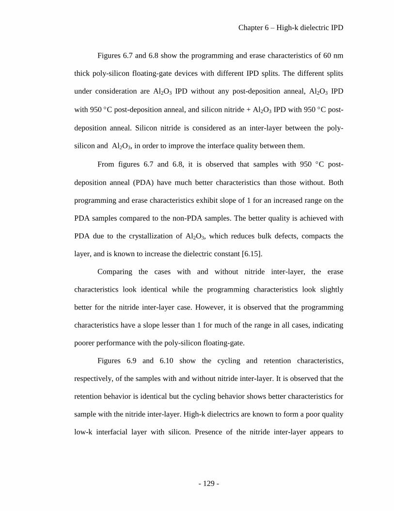
Chapter 6 – High-k dielectric IPD
- 129 -
Figures 6.7 and 6.8 show the programming and erase characteristics of 60 nm
thick poly-silicon floating-gate devices with different IPD splits. The different splits
under consideration are Al2O3 IPD without any post-deposition anneal, Al2O3 IPD
with 950 C post-deposition anneal, and silicon nitride + Al2O3 IPD with 950 C post-
deposition anneal. Silicon nitride is considered as an inter-layer between the poly-
silicon and Al2O3, in order to improve the interface quality between them.
From figures 6.7 and 6.8, it is observed that samples with 950 C post-
deposition anneal (PDA) have much better characteristics than those without. Both
programming and erase characteristics exhibit slope of 1 for an increased range on the
PDA samples compared to the non-PDA samples. The better quality is achieved with
PDA due to the crystallization of Al2O3, which reduces bulk defects, compacts the
layer, and is known to increase the dielectric constant [6.15].
Comparing the cases with and without nitride inter-layer, the erase
characteristics look identical while the programming characteristics look slightly
better for the nitride inter-layer case. However, it is observed that the programming
characteristics have a slope lesser than 1 for much of the range in all cases, indicating
poorer performance with the poly-silicon floating-gate.
Figures 6.9 and 6.10 show the cycling and retention characteristics,
respectively, of the samples with and without nitride inter-layer. It is observed that the
retention behavior is identical but the cycling behavior shows better characteristics for
sample with the nitride inter-layer. High-k dielectrics are known to form a poor quality
low-k interfacial layer with silicon. Presence of the nitride inter-layer appears to

Chapter 6 – High-k dielectric IPD
- 130 -
suppress that, and improve the quality of the interface with the poly-silicon floating-
gate.
Figure 6.7: Program characteristics of 60 nm poly-silicon floating-gate devices with different IPD
layers.
Figure 6.8: Erase characteristics of 60 nm poly-silicon floating-gate devices with different IPD layers.
-3
-2
-1
0
1
2
3
4
5
6
7
8
8 10 12 14 16 18 20 22 24
VFB
(V)
VPROG(V)
Al2O3 (No PDA)
Al2O3 (950 C PDA)
Nitride + Al2O3 (950 C PDA)
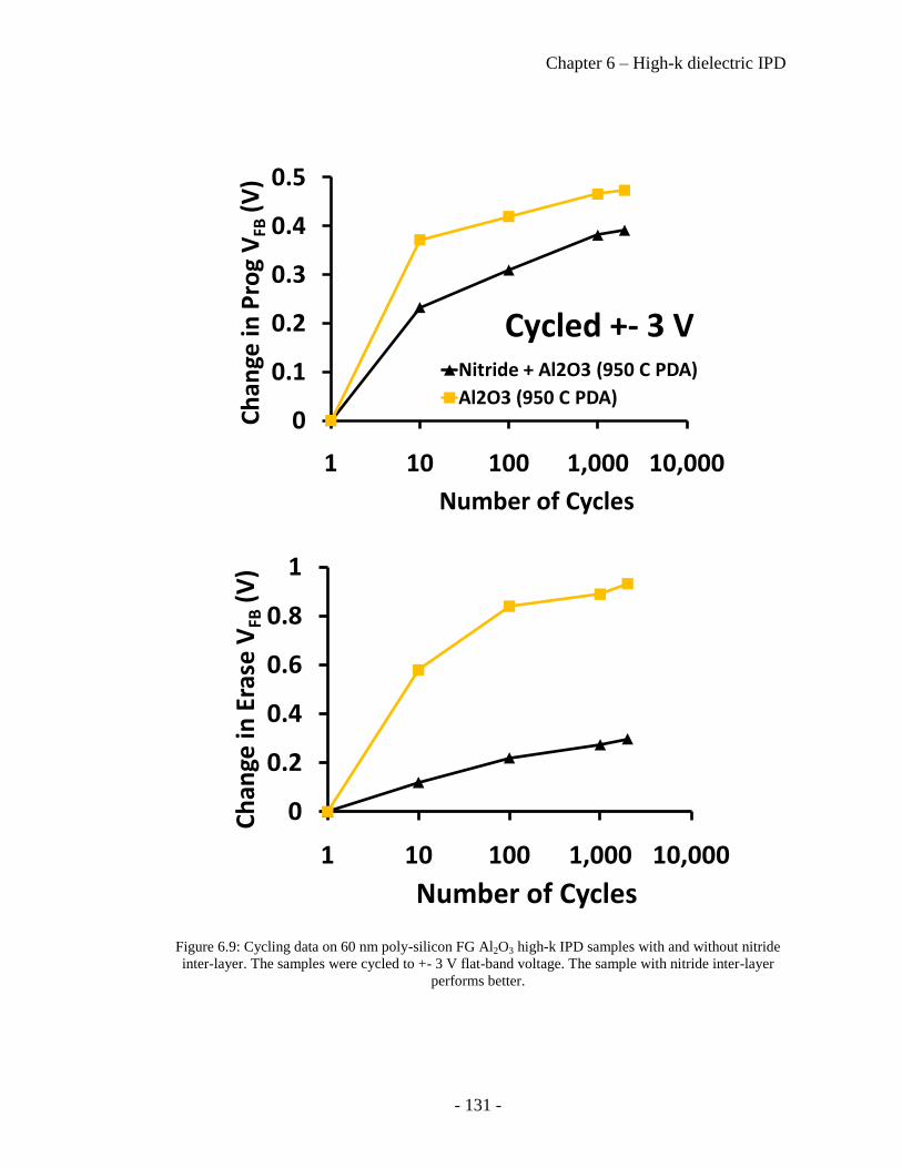
Chapter 6 – High-k dielectric IPD
- 131 -
Figure 6.9: Cycling data on 60 nm poly-silicon FG Al2O3 high-k IPD samples with and without nitride
inter-layer. The samples were cycled to +- 3 V flat-band voltage. The sample with nitride inter-layer
performs better.
0
0.1
0.2
0.3
0.4
0.5
1 10 100 1,000 10,000
Ch
ange
in P
rog
VFB
(V)
Number of Cycles
Nitride + Al2O3 (950 C PDA)
Al2O3 (950 C PDA)
Cycled +- 3 V
0
0.2
0.4
0.6
0.8
1
1 10 100 1,000 10,000
Ch
ange
in E
rase
VFB
(V)
Number of Cycles

Chapter 6 – High-k dielectric IPD
- 132 -
Figure 6.10: Retention characteristics for 60 nm poly-silicon FG Al2O3 high-k IPD device with and
without nitride interlayer.
The nitride + Al2O3 IPD, identified so far as the best option, is integrated with
poly-silicon FG layers of various thicknesses. Figures 6.11 and 6.12 present the
programming and erase characteristics of poly-silicon FG devices (7 to 60 nm) with
nitride + Al2O3 IPD. It is observed that the programming and erase characteristics of
thin poly-silicon floating-gate devices are matched to those of thick poly-silicon
floating-gate devices. The slope is lesser than 1 for much of the programming region,
as discussed before.
Figure 6.13 shows endurance characteristics for these devices. It is observed
that the thick poly-silicon floating-gate device performs much better than the ultra-thin
7 nm poly-silicon floating-gate device. This is expected, because the ultra-thin 7 nm
poly-silicon floating-gate device suffers from ballistic carrier damage.
-4
-2
0
2
4
1 10 100 1000 10000
VFB
(V)
Time (s), 150 C Bake
Al2O3 (950 C PDA)
Nitride + Al2O3 (950 C PDA)

Chapter 6 – High-k dielectric IPD
- 133 -
Figure 6.11: Program characteristics of poly-silicon FG devices of various thicknesses with nitride +
Al2O3 high-k IPD.
Figure 6.12: Erase characteristics of poly-silicon FG devices of various thicknesses with nitride + Al2O3
high-k IPD.
0
1
2
3
4
5
6
7
8 10 12 14 16 18 20 22
VFB
(V)
VPROG(V)
7 nm poly-Si FG10 nm poly-Si FG60 nm poly-Si FG
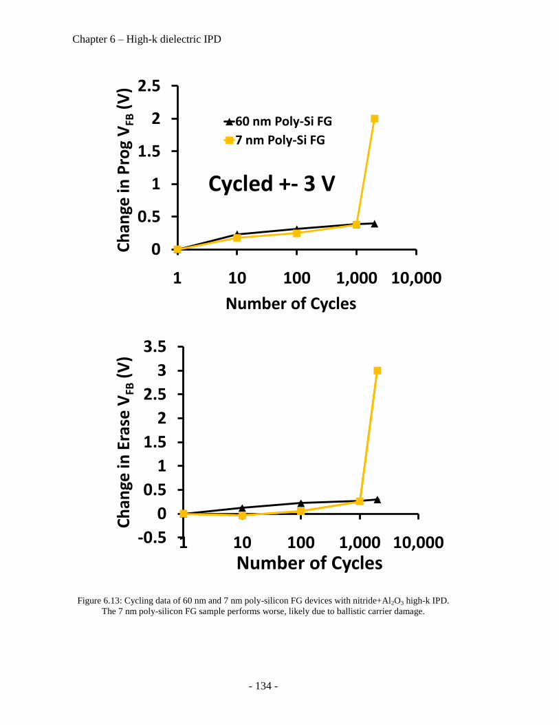
Chapter 6 – High-k dielectric IPD
- 134 -
Figure 6.13: Cycling data of 60 nm and 7 nm poly-silicon FG devices with nitride+Al2O3 high-k IPD.
The 7 nm poly-silicon FG sample performs worse, likely due to ballistic carrier damage.
0
0.5
1
1.5
2
2.5
1 10 100 1,000 10,000
Ch
ange
in P
rog
VFB
(V)
Number of Cycles
60 nm Poly-Si FG
7 nm Poly-Si FG
Cycled +- 3 V
-0.5
0
0.5
1
1.5
2
2.5
3
3.5
1 10 100 1,000 10,000
Ch
ange
in E
rase
VFB
(V)
Number of Cycles
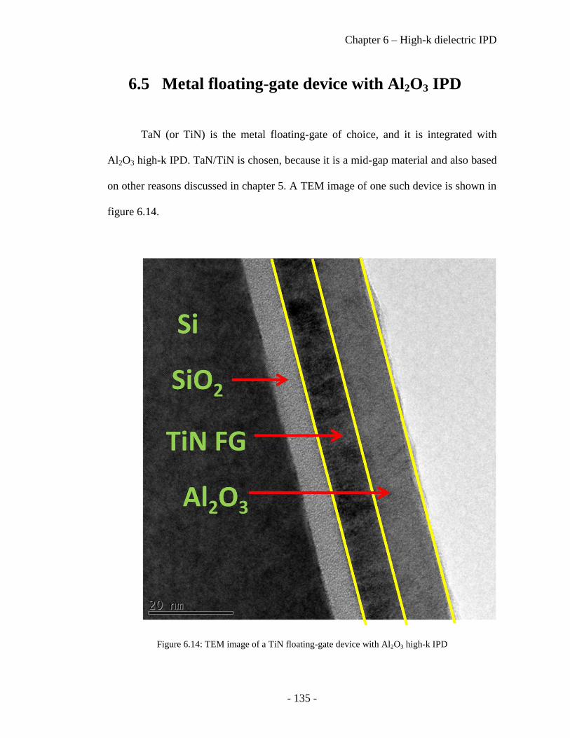
Chapter 6 – High-k dielectric IPD
- 135 -
6.5 Metal floating-gate device with Al2O3 IPD
TaN (or TiN) is the metal floating-gate of choice, and it is integrated with
Al2O3 high-k IPD. TaN/TiN is chosen, because it is a mid-gap material and also based
on other reasons discussed in chapter 5. A TEM image of one such device is shown in
figure 6.14.
Figure 6.14: TEM image of a TiN floating-gate device with Al2O3 high-k IPD

Chapter 6 – High-k dielectric IPD
- 136 -
The programming and erase characteristics of a TaN metal floating-gate device
with Al2O3 high-k IPD are presented in figures 6.15 and 6.16 along with poly-silicon
floating-gate sample data for comparison.
It is observed that the metal has much better program characteristics with a
slope of 1 for a wider range. It is also observed that the metal erases slower due to the
deeper work-function compared to n+ poly-silicon floating-gate.
The retention and endurance data of these TaN samples is presented in figures
6.17 and 6.18 respectively. It is observed that the retention of these samples is very
good as expected for a mid-gap floating-gate material like TaN. It is also observed that
the cycling behavior is reasonably good. It can be improved further by optimizing the
process more, better understanding the tunnel oxide–metal interface, and improving
techniques to deposit dielectrics on metals.
Figure 6.15: Program characteristics of TaN FG compared to poly-silicon FG, both with high-k IPD.
0
1
2
3
4
5
6
8 10 12 14 16 18 20
VFB
(V)
VPROG(V)
TaN FG
Poly-Si FG

Chapter 6 – High-k dielectric IPD
- 137 -
Figure 6.16: Erase of TaN FG compared to poly-silicon FG, both with high-k IPD.
Figure 6.17: Retention of TaN FG device with high-k IPD
-4
-3
-2
-1
0
1
2
3
4
1 10 100 1000 10000
VFB
(V)
Time (s), 150 C Bake

Chapter 6 – High-k dielectric IPD
- 138 -
Figure 6.18: Endurance data for TaN FG device with Al2O3 high-k IPD
0
0.2
0.4
0.6
0.8
1 100 10,000Ch
ange
in P
rog
VFB
(V)
Number of Cycles
Cycled +- 3 V
0
0.1
0.2
0.3
0.4
0.5
1 100 10,000Ch
ange
in E
rase
VFB
(V)
Number of Cycles

Chapter 6 – High-k dielectric IPD
- 139 -
6.6 Control-Gate
The control-gate work-function is an important parameter because it
determines the gate-injection, and consequently the erase-saturation. As shown in
figure 6.19, the deeper the work-function of the control-gate, the lesser the gate-
injection is. This is especially important, given the use of deeper work-function metal
floating-gates which erase slower.
This is experimentally confirmed through the data shown in figure 6.20, for
devices with aluminum control gate versus platinum control gate. The deeper work-
function platinum control-gate device performs better with respect to erase-saturation,
compared to the shallower work-function aluminum.
6.7 Summary
The replacement of the conventional oxide-nitride IPD in floating-gate NAND
flash devices with high-k dielectric IPD was explored. The requirements of the high-k
material for use as IPD were discussed. Both poly-silicon and metal floating-gate
devices were integrated with Al2O3 IPD, and their electrical characteristics were
presented. The role of the work-function of the control-gate was clarified.

Chapter 6 – High-k dielectric IPD
- 140 -
Figure 6.19: Band diagrams depicting deeper work-function metal with lesser gate-injection.

Chapter 6 – High-k dielectric IPD
- 141 -
Figure 6.20: Pt CG (deeper work-function) showing improved erase saturation compared to Al CG
(shallower work-function)

Chapter 6 – High-k dielectric IPD
- 142 -
References
[6.1] International Technology Roadmap for Semiconductors: Process
Integration, Devices and Structures, 2009 edition.
[6.2] Govoreanu et. al, " Scaling down the interpoly dielectric for next
generation Flash memory: Challenges and opportunities”, Solid-state electronics,
Vol.49, Iss.11, Nov 2005.
[6.3] J.D.Lee, S.H.Hur and J.L.Choi, "Effects of Floating-Gate Interference on
NAND Flash Memory Cell Operation", IEEE Electron Device Letters, p.264, Vol.23,
Issue 5, May 2002.
[6.4] K.Kim, “Technology for sub-50nm DRAM and NAND flash
manufacturing “, IEDM 2005.
[6.5] J. De Vos et.al., European Solid-State Device Research Conference
(ESSDERC) 2008.
[6.6] Shyam Raghunathan, Tejas Krishnamohan, Krishna Parat and Krishna
Saraswat, “Investigation of Ballistic Current in Scaled Floating-gate NAND Flash and
a Solution”, Proceedings of the Internation Electron Devices Meeting 2009.
[6.7] Barbara De Salvo, Silicon non-volatile memories: paths of innovation,
ISTE John Wiley 2009.
[6.8] A.Fazio (Intel), “Challenges in charge based flash memory & phase
change memory”, EE310 Seminar, Stanford University, January 2007.
[6.9] Dong-Chan Kim, et al., “A 2 Gb NAND flash memory with 0.044 μm2
cell size using 90 nm flash technology”, IEDM 2002.

Chapter 6 – High-k dielectric IPD
- 143 -
[6.10] ITRS Table PIDS5, 2009.
[6.11] Jong-Ho Park et.al. (Samsung), “8 Gb MLC (multi-level cell) NAND
flash memory using 63 nm process technology”, IEDM 2004.
[6.12] Kinam Kim, Jungdal Choi, “Future Outlook of NAND Flash
Technology for 40 nm node and beyond”, pp 9-11, NVSMW 2006.
[6.13] Peter Blomme and J.Van Houdt, “Scalability of fully planar NAND
flash memory arrays below 45 nm”, pg.51, International Memory Workshop 2009.
[6.14] Robertson, J., “Band structures and band offsets of high k dielectrics on
Si”, Appl. Surf. Sci. 190 (1-4) (2002).
[6.15] D.Shum et. al., “ALD-Al2O3 as an Inter-Poly dielectric for a product
demonstrator in a proven eFlash technology”, pg.42, International Memory Workshop
2009.

Chapter 6 – High-k dielectric IPD
- 144 -
This page is intentionally left blank

Chapter 7 – Conclusions and Future Directions
- 145 -
Chapter 7
Conclusions and Future Directions
7.1 The Planar Floating-Gate Device
The planar floating-gate device with ultra-thin metal floating-gate, high-k IPD
and deep work-function control gate, is proposed to extend scaling of NAND flash
memories. The device is shown in figure 7.1. The development of the device came
about as follows:
Cell-to-cell interference was identified as a major barrier in the
continued scaling of NAND flash memories. In order to overcome this
interference issue, the floating-gate was proposed to be scaled.
Poly-silicon floating-gate scaling was studied in detail, and these
devices were scaled down to ultra-thin 7 nm poly-silicon floating-gate
thickness, which was the thinnest reported at the time.

Chapter 7 – Conclusions and Future Directions
- 146 -
Figure 7.1: The planar (no wrap) floating-gate device
A new reliability failure mechanism was proposed and demonstrated
for the first time. This mechanism is due to programming carriers going
increasingly ballistic through the ultra-thin poly-silicon floating-gates.
These high energy ballistic carriers pose a reliability risk to the IPD.
A new test structure was developed to study the ballistic carrier issue,
and was used to extract the inelastic mean free path of electrons in
poly-silicon.
Poly-silicon was demonstrated to have scaling issues due to the ballistic
carrier issue, poly-depletion etc.

Chapter 7 – Conclusions and Future Directions
- 147 -
Metal-based floating-gate was proposed to overcome challenges of the
poly-silicon floating-gate, and demonstrated for the first time.
Metal floating-gate was shown to successfully overcome ballistic and
other issues, and demonstrated excellent electrical characteristics.
The effect of metal floating-gate work-function was studied, and mid-
gap materials, e.g. TiN/TaN, were chosen as the preferred floating-gate
material.
The TiN floating-gate was scaled down to ultra-thin 3 nm, exhibiting
excellent performance, and reducing cell-to-cell interference greatly
due to its very small thickness.
High-k dielectric was proposed to replace conventional IPD in order to
compensate loss of GCR caused by lack of CG wrap-around.
The factors underlying choice of high-k dielectric were discussed and
Al2O3 was picked.
Both poly-silicon and metal floating-gate devices were integrated with
Al2O3 high-k IPD.
Use of a silicon nitride inter-layer improved the quality of the Al2O3
IPD on poly-silicon floating-gates.
TaN floating-gate devices with high-k IPD were shown to have better
programming characteristics than poly-silicon floating-gate devices
with high-k IPD. The TaN floating-gate devices erased slower due to
the deeper work-function. Overall, the TaN devices had very good
electrical performance.

Chapter 7 – Conclusions and Future Directions
- 148 -
A deeper work-function control-gate was shown to reduce gate-
injection, and consequently erase-saturation.
Combining all these layers, as shown in figure 7.1, we get the planar
(no wrap) floating-gate device with ultra-thin TiN/TaN floating-gate,
Al2O3 high-k IPD and deep work-function control gate. This structure
would allow us to extend scaling of NAND flash memories.
7.2 Future Directions
Tunnel oxide thickness scaling has essentially stopped. Work on
barrier-engineered layers is an important area that has potential.
The process steps involved in the planar floating-gate device need to be
further optimized. For example, there needs to be better understanding
for deposition of high quality high-k dielectrics on metals, and
interaction of the metal-tunnel oxide interface.
As the cell becomes smaller and smaller, it will be limited by the
number of electrons stored. At that point, instead of scaling cell-area, it
is better to integrate cells in 3D to increase density. Work towards this,
like the bit cost scalable (BiCS) cell by Toshiba, is an important
direction of research.
At those ultra-small dimensions, as the flash cell becomes intrinsically
limited, non-charge based cells like ferro-electric RAM (FeRAM),

Chapter 7 – Conclusions and Future Directions
- 149 -
magnetic RAM (MRAM), phase change RAM (PCRAM) and
resistance change RAM (ReRAM) are promising alternatives.
Figure 7.2 shows potential solutions for non-volatile memory, as projected by
ITRS.
Figure 7.2: Non-volatile memory potential solutions (Source: ITRS 2009)