saw rf filter, b3440 - rf360 - home components b3440 saw rf filter 869 mhz data sheet table of...
TRANSCRIPT

RF360 Europe GmbH
A Qualcomm – TDK Joint Venture
®
RF360 products mentioned within this document are offered by RF360 Europe GmbH and other subsidiaries ofRF360 Holdings Singapore Pte. Ltd. (collectively, the “RF360 Subsidiaries”). RF360 Holdings Singapore Pte. Ltd.is a joint venture of Qualcomm Global Trading Pte. Ltd. and EPCOS AG. References in this documentation toEPCOS AG should properly reference, and shall be read to reference, the RF360 Subsidiaries.
RF360 Europe GmbH, Anzinger Str. 13, München, Germany
© 2016 RF360 Europe GmbH and/or its affiliated companies. All rights reserved.
SAW components
SAW RF filterShort range devices
Series/type: B3440Ordering code: B39871B3440U410
Date: September 29, 2016Version: 2.3

These materials, including the information contained herein, may be used only for informational purposes by the customer. The RF360 Subsidiaries assume no responsibility for errors or omissions in these materials or the information contained herein. The RF360 Subsidiaries reserve the right to make changes to the product(s) or information contained herein without notice. The materials and information are provided on an AS IS basis, and the RF360 Subsidiaries assume no liability and make no warranty or representation, either expressed or implied, with respect to the materials, or any output or results based on the use, application, or evaluation of such materials, including, without limitation, with respect to the non-infringement of trademarks, patents, copyrights or any other intellectual property rights or other rights of third parties.
No use of this documentation or any information contained herein grants any license, whether express, implied, by estoppel or otherwise, to any intellectual property rights, including, without limitation, to any patents owned by QUALCOMM Incorporated or any of its subsidiaries.
Not to be used, copied, reproduced, or modified in whole or in part, nor its contents revealed in any manner to others without the express written permission of RF360 Europe GmbH.
Qualcomm and Qualcomm RF360 are trademarks of Qualcomm Incorporated, registered in the United States and other countries. RF360 is a trademark of Qualcomm Incorporated. Other product and brand names may be trademarks or registered trademarks of their respective owners.
This technical data may be subject to U.S. and international export, re-export, or transfer (“export”) laws. Diversion contrary to U.S. and international law is strictly prohibited.

SAW components
SAW RF filterShort range devices
Series/type: B3440
Ordering code: B39871B3440U410
Date: September 29, 2016
Version: 2.3
© EPCOS AG 2016. Reproduction, publication and dissemination of this data sheet, enclosures hereto and the information contained therein without EPCOS’ prior express consent is prohibited.
EPCOS AG is a TDK Group Company.
SAW components B3440
SAW RF filter 869 MHz
Data sheet
Table of contents
1 Application......................................................................................................................................... 32 Features............................................................................................................................................ 33 Package............................................................................................................................................ 44 Pin configuration................................................................................................................................45 Matching circuit.................................................................................................................................56 Characteristics...................................................................................................................................67 Maximum ratings...............................................................................................................................78 Transmission coefficient....................................................................................................................89 Reflection coefficients........................................................................................................................910 Packing material............................................................................................................................1011 Marking.......................................................................................................................................... 1212 Soldering profile.............................................................................................................................1313 ESD protection of SAW filters........................................................................................................1414 Annotations...................................................................................................................................1515 Cautions and warnings..................................................................................................................16 Important notes.................................................................................................................................17
Please read Cautions and warnings and Page 2 of 17 September 29, 2016Important notes at the end of this document.
SAW components B3440
SAW RF filter 869 MHz
Data sheet
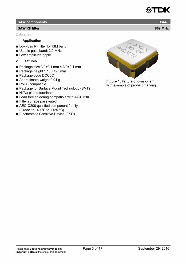
1 Application
Low-loss RF filter for ISM band Usable pass band: 2.0 MHz Low amplitude ripple
2 Features
Package size 3.0±0.1 mm × 3.0±0.1 mm Package height 1.1±0.125 mm Package code DCC6C Approximate weight 0.04 g RoHS compatible Package for Surface Mount Technology (SMT) Ni/Au-plated terminals Lead free soldering compatible with J-STD20C Filter surface passivated AEC-Q200 qualified component family
(Grade 1: −40 °C to +125 °C) Electrostatic Sensitive Device (ESD)
Please read Cautions and warnings and Page 3 of 17 September 29, 2016Important notes at the end of this document.
Figure 1: Picture of componentwith example of product marking.
SAW components B3440
SAW RF filter 869 MHz
Data sheet
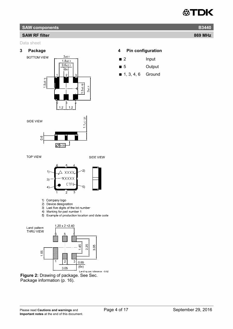
3 Package 4 Pin configuration
2 Input
5 Output
1, 3, 4, 6 Ground
Please read Cautions and warnings and Page 4 of 17 September 29, 2016Important notes at the end of this document.
Figure 2: Drawing of package. See Sec.Package information (p. 16).
SAW components B3440
SAW RF filter 869 MHz
Data sheet
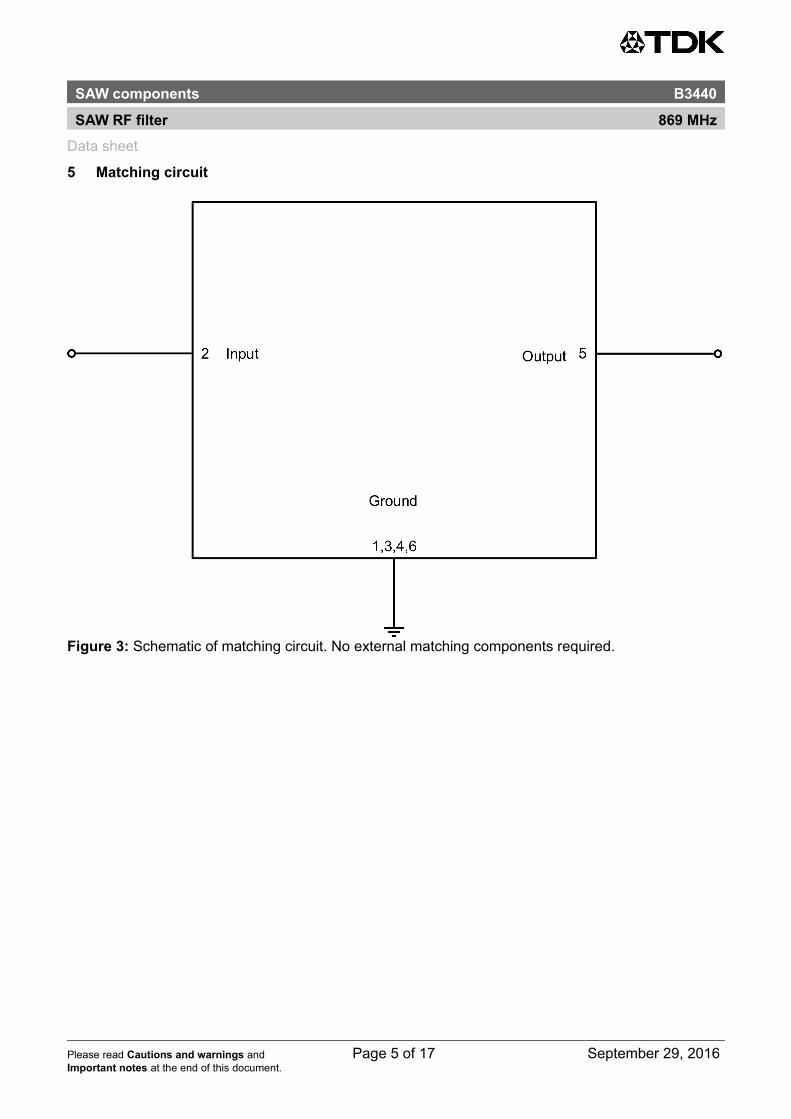
5 Matching circuit
Please read Cautions and warnings and Page 5 of 17 September 29, 2016Important notes at the end of this document.
Figure 3: Schematic of matching circuit. No external matching components required.

SAW components B3440
SAW RF filter 869 MHz
Data sheet
6 Characteristics
Temperature range for specification TSPEC
= −40 °C ... +105 °C
Input terminating impedance ZIN
= 50 Ω
Output terminating impedance ZOUT
= 50 Ω
Characteristics min.for T
SPEC
typ.@ +25 °C
max.for T
SPEC
Center frequency fC
— 869 — MHz
Maximum insertion attenuation αmax
868... 870 MHz — 2.6 3.2 dB
Amplitude ripple (p-p) Δα
868... 870 MHz — 0.4 1.0 dB
Maximum VSWR VSWRmax
@ input port 868... 870 MHz — 1.3 1.6
@ output port 868... 870 MHz — 1.3 1.6
Minimum attenuation αmin
50... 791 MHz 43 46 — dB
791... 835 MHz 50 54 — dB
835... 848 MHz 42 45 — dB
848... 862 MHz 301) 41 — dB
848... 862 MHz 28 41 — dB
880... 883 MHz 25 35 — dB
883... 1000 MHz 49 54 — dB1) Valid for temperature T = −40 °C...+80 °C.
Please read Cautions and warnings and Page 6 of 17 September 29, 2016Important notes at the end of this document.

SAW components B3440
SAW RF filter 869 MHz
Data sheet
7 Maximum ratings
Operable temperature TOP
= −45 °C ... +125 °C
Storage temperature TSTG
1) = −45 °C ... +125 °C
DC voltage |VDC
| = 6.0 V (max.)
Source power PS
= 18 dBm Source impedance 50 Ω.
1) Not valid for packaging material. Storage temperature for packaging material is −25 °C to +40 °C.
Please read Cautions and warnings and Page 7 of 17 September 29, 2016Important notes at the end of this document.
SAW components B3440
SAW RF filter 869 MHz
Data sheet
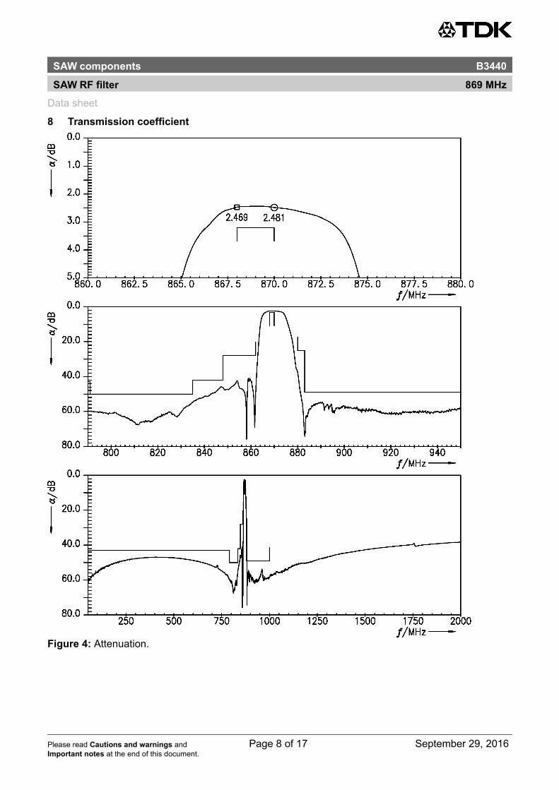
8 Transmission coefficient
Please read Cautions and warnings and Page 8 of 17 September 29, 2016Important notes at the end of this document.
Figure 4: Attenuation.
SAW components B3440
SAW RF filter 869 MHz
Data sheet
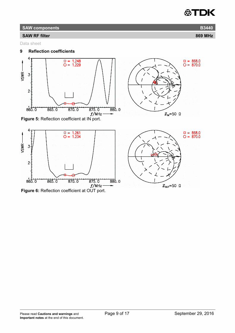
9 Reflection coefficients
Figure 5: Reflection coefficient at IN port.
Figure 6: Reflection coefficient at OUT port.
Please read Cautions and warnings and Page 9 of 17 September 29, 2016Important notes at the end of this document.

SAW components B3440
SAW RF filter 869 MHz
Data sheet
10 Packing material
10.1 Tape
A0 3.25±0.1 mm E2 10.25 mm (min.) P1 4.0±0.1 mm
B0 3.3±0.1 mm F 5.5±0.05 mm P2 2.0±0.1 mm
D0 1.5+0.1/−0 mm G 0.75 mm (min.) T 0.2±0.05 mm
D1 1.5 mm (min.) K0 1.5±0.1 mm W 12.0+0.3/−0.1 mm
E1 1.75±0.1 mm P0 4.0±0.1 mm
Table 1: Tape dimensions.
Please read Cautions and warnings and Page 10 of 17 September 29, 2016Important notes at the end of this document.
Figure 7: Drawing of tape (first-angle projection) with tape dimensions according to Table 1.
SAW components B3440
SAW RF filter 869 MHz
Data sheet
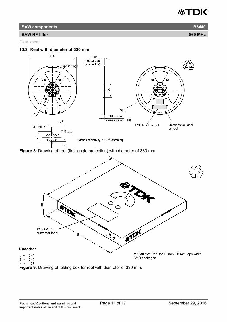
10.2 Reel with diameter of 330 mm
Figure 8: Drawing of reel (first-angle projection) with diameter of 330 mm.
Figure 9: Drawing of folding box for reel with diameter of 330 mm.
Please read Cautions and warnings and Page 11 of 17 September 29, 2016Important notes at the end of this document.

SAW components B3440
SAW RF filter 869 MHz
Data sheet
11 Marking
Products are marked with device designation, lot number, as well as production location and date code.
Device designation: The 4-character device designation of the ordering code is used for the marking.
Example for 4-character device designation: B3xxxxB1234xxxx
Lot number: The last 5 digits of the lot number are used for the marking.
Example: 12345
Production location and date code: The production location is Wuxi (encoded in the first character 'C'). The production date code is encoded in the last three characters according to Table 2.
1st digit (day) 2nd digit (year) 3rd digit (month)
Day Code Day Code Day Code Year Code Year Code Month Code Month Code
1 1 11 A 21 M 2010 A 2022 P Jan 1 Jul 7
2 2 12 B 22 N 2011 B 2023 R Feb 2 Aug 8
3 3 13 C 23 P 2012 C 2024 S Mar 3 Sep 9
4 4 14 D 24 R 2013 D 2025 T Apr 4 Oct 0
5 5 15 E 25 S 2014 E 2026 U May 5 Nov N
6 6 16 F 26 T 2015 F 2027 V Jun 6 Dec D
7 7 17 H 27 U 2016 H 2028 W
8 8 18 J 28 V 2017 J 2029 X
9 9 19 K 29 W 2018 K 2030 Z
10 0 20 L 30 X 2019 L 2031 A
31 Z 2020 M 2032 B
2021 N and so on
Table 2: Production date code.
Example of how to decode production location and date code:
Code: C T F 6
Location: C → WuxiDay: T → 26th
Year: F → 2015Month: 6 → June
Please read Cautions and warnings and Page 12 of 17 September 29, 2016Important notes at the end of this document.

SAW components B3440
SAW RF filter 869 MHz
Data sheet
12 Soldering profile
The recommended soldering process is in accordance with IEC 60068-2-58 – 3rd edit and IPC/JEDECJ-STD-020B.
Please read Cautions and warnings and Page 13 of 17 September 29, 2016Important notes at the end of this document.
Figure 10: Recommended reflow profile for convection and infrared soldering – lead-free solder.
ramp rate ≤ 3 K/s
preheat 125 °C to 220 °C, 150 s to 210 s, 0.4 K/s to 1.0 K/s
T > 220 °C 30 s to 70 s
T > 230 °C min. 10 s
T > 245 °C max. 20 s
T ≥ 255 °C –
peak temperature Tpeak 250 °C +0/-5 °C
wetting temperature Tmin 230 °C +5/-0 °C for 10 s ± 1 s
cooling rate ≤ 3 K/s
soldering temperature T measured at solder pads
Table 3: Characteristics of recommended soldering profile for lead-free solder (Sn95.5Ag3.8Cu0.7).

SAW components B3440
SAW RF filter 869 MHz
Data sheet
13 ESD protection of SAW filters
SAW filters are Electro Static Discharge sensitive devices. To reduce the probability of damages caused by ESD, special matching topologies have to be applied.
In general, “ESD matching” has to be ensured at that filter port, where electrostatic discharge is expected.
Electrostatic discharges predominantly appear at the antenna input of RF receivers. Therefore, only the input matching of the SAW filter has to be designed to short circuit or to block the ESD pulse.
Below three figures show recommended “ESD matching” topologies.
For wide band filters the high-pass ESD matching structure needs to be at least of 3rd order to ensure a proper matching for any impedance value of antenna and SAW filter input. The required componentvalues have to be determined from case to case.
In cases where minor ESD occur, following simplified “ESD matching” topologies can be used alternatively.
In all three figures the shunt inductor Lp2 could be replaced by a shorted microstrip with proper length and width. If this configuration is possible depends on the operating frequency and available PCB space.
Effectiveness of the applied ESD protection has to be checked according to relevant industry standards or customer specific requirements.
For further information, please refer to EPCOS Application report: “ESD protection for SAW filters”.This report can be found under www.epcos.com/rke. Click on “Applications Notes”.
Please read Cautions and warnings and Page 14 of 17 September 29, 2016Important notes at the end of this document.
Figure 13: 3rd order high-pass structure for basic ESD protection.
Figure 12: Suppressor diode plus ESD matching.
Figure 11: MLC varistor plus ESD matching.
SAW components B3440
SAW RF filter 869 MHz
Data sheet
14 Annotations
14.1 Matching coils
See TDK inductor pdf-catalog http://www.tdk.co.jp/tefe02/coil.htm#aname1 and Data Library for circuitsimulation http://www.tdk.co.jp/etvcl/index.htm.
14.2 RoHS compatibility
ROHS-compatible means that products are compatible with the requirements according to Art. 4 (substance restrictions) of Directive 2011/65/EU of the European Parliament and of the Council of June 8th, 2011, on the restriction of the use of certain hazardous substances in electrical and electronic equipment ("Directive") with due regard to the application of exemptions as per Annex III of the Directive in certain cases.
14.3 Scattering parameters (S-parameters)
The pin/port assignment is available in the headers of the S-parameter files. Please contact your localEPCOS sales office.
Please read Cautions and warnings and Page 15 of 17 September 29, 2016Important notes at the end of this document.
SAW components B3440
SAW RF filter 869 MHz
Data sheet
15 Cautions and warnings
15.1 Display of ordering codes for EPCOS products
The ordering code for one and the same product can be represented differently in data sheets, data books, other publications and the website of EPCOS, or in order-related documents such as shipping notes, order confirmations and product labels. The varying representations of the ordering codes are due to different processes employed and do not affect the specifications of the respective products. Detailed information can be found on the Internet under www.epcos.com/orderingcodes.
15.2 Material information
Due to technical requirements components may contain dangerous substances. For information on the type in question please also contact one of our sales offices.
For information on recycling of tapes and reels please contact one of our sales offices.
15.3 Moldability
Before using in overmolding environment, please contact your local EPCOS sales office.
15.4 Package information
Landing area
The printed circuit board (PCB) land pattern (landing area) shown is based on EPCOS internal development and empirical data and illustrated for example purposes, only. As customers' SMD assembly processes may have a plenty of variants and influence factors which are not under control or knowledge of EPCOS, additional careful process development on customer side is necessary and strongly recommended in order to achieve best soldering results tailored to the particular customer needs.
Dimensions
Unless otherwise specified all dimensions are understood using unit millimeter (mm).
Projection method
Unless otherwise specified first-angle projection is applied.
Please read Cautions and warnings and Page 16 of 17 September 29, 2016Important notes at the end of this document.
Important notes
The following applies to all products named in this publication:
1. Some parts of this publication contain statements about the suitability of our products forcertain areas of application. These statements are based on our knowledge of typicalrequirements that are often placed on our products in the areas of application concerned. Wenevertheless expressly point out that such statements cannot be regarded as bindingstatements about the suitability of our products for a particular customer application.As a rule, EPCOS is either unfamiliar with individual customer applications or less familiar withthem than the customers themselves. For these reasons, it is always ultimately incumbent onthe customer to check and decide whether an EPCOS product with the properties described inthe product specification is suitable for use in a particular customer application.
2. We also point out that in individual cases, a malfunction of electronic components orfailure before the end of their usual service life cannot be completely ruled out in thecurrent state of the art, even if they are operated as specified. In customer applicationsrequiring a very high level of operational safety and especially in customer applications inwhich the malfunction or failure of an electronic component could endanger human life orhealth (e.g. in accident prevention or life-saving systems), it must therefore be ensured bymeans of suitable design of the customer application or other action taken by the customer(e.g. installation of protective circuitry or redundancy) that no injury or damage is sustained bythird parties in the event of malfunction or failure of an electronic component.
3. The warnings, cautions and product-specific notes must be observed.
4. In order to satisfy certain technical requirements, some of the products described in thispublication may contain substances subject to restrictions in certain jurisdictions (e.g.because they are classed as hazardous). Useful information on this will be found in ourMaterial Data Sheets on the Internet (www.epcos.com/material). Should you have any moredetailed questions, please contact our sales offices.
5. We constantly strive to improve our products. Consequently, the products described in thispublication may change from time to time. The same is true of the corresponding productspecifications. Please check therefore to what extent product descriptions and specificationscontained in this publication are still applicable before or when you place an order.We also reserve the right to discontinue production and delivery of products.Consequently, we cannot guarantee that all products named in this publication will always beavailable. The aforementioned does not apply in the case of individual agreements deviating from theforegoing for customer-specific products.
6. Unless otherwise agreed in individual contracts, all orders are subject to the currentversion of the “General Terms of Delivery for Products and Services in the ElectricalIndustry” published by the German Electrical and Electronics Industry Association(ZVEI).
7. The trade names EPCOS, CeraDiode, CeraLink, CeraPad, CeraPlas, CSMP, CSSP, CTVS,DeltaCap, DigiSiMic, DSSP, ExoCore, FilterCap, FormFit, LeaXield, MiniBlue, MiniCell, MKD,MKK, MotorCap, PCC, PhaseCap, PhaseCube, PhaseMod, PhiCap, PQSine, SIFERRIT, SIFI,SIKOREL, SilverCap, SIMDAD, SiMic, SIMID, SineFormer, SIOV, SIP5D, SIP5K, TFAP,ThermoFuse, WindCap are trademarks registered or pending in Europe and in othercountries. Further information will be found on the Internet at www.epcos.com/trademarks.
Page 17 of 17
Important notes