saw duplexer, b8635 - en.rf360jv.com · electrostatic sensitive device (esd). moisture sensitivity...
TRANSCRIPT

RF360 Europe GmbH
A Qualcomm – TDK Joint Venture
®
RF360 products mentioned within this document are offered by RF360 Europe GmbH and other subsidiaries ofRF360 Holdings Singapore Pte. Ltd. (collectively, the “RF360 Subsidiaries”). RF360 Holdings Singapore Pte. Ltd.is a joint venture of Qualcomm Global Trading Pte. Ltd. and EPCOS AG. References in this documentation toEPCOS AG should properly reference, and shall be read to reference, the RF360 Subsidiaries.
RF360 Europe GmbH, Anzinger Str. 13, München, Germany
© 2016 RF360 Europe GmbH and/or its affiliated companies. All rights reserved.
SAW Components
SAW DuplexerWCDMA / LTE Band 1
Series/type: B8635Ordering code: B39212B8635P810
Date: September 15, 2015Version: 2.4

These materials, including the information contained herein, may be used only for informational purposes by the customer. The RF360 Subsidiaries assume no responsibility for errors or omissions in these materials or the information contained herein. The RF360 Subsidiaries reserve the right to make changes to the product(s) or information contained herein without notice. The materials and information are provided on an AS IS basis, and the RF360 Subsidiaries assume no liability and make no warranty or representation, either expressed or implied, with respect to the materials, or any output or results based on the use, application, or evaluation of such materials, including, without limitation, with respect to the non-infringement of trademarks, patents, copyrights or any other intellectual property rights or other rights of third parties.
No use of this documentation or any information contained herein grants any license, whether express, implied, by estoppel or otherwise, to any intellectual property rights, including, without limitation, to any patents owned by QUALCOMM Incorporated or any of its subsidiaries.
Not to be used, copied, reproduced, or modified in whole or in part, nor its contents revealed in any manner to others without the express written permission of RF360 Europe GmbH.
Qualcomm and Qualcomm RF360 are trademarks of Qualcomm Incorporated, registered in the United States and other countries. RF360 is a trademark of Qualcomm Incorporated. Other product and brand names may be trademarks or registered trademarks of their respective owners.
This technical data may be subject to U.S. and international export, re-export, or transfer (“export”) laws. Diversion contrary to U.S. and international law is strictly prohibited.

SAW Components
SAW DuplexerWCDMA / LTE Band 1
Series/type: B8635
Ordering code: B39212B8635P810
Date: September 15, 2015
Version: 2.4
© EPCOS AG 2015. Reproduction, publication and dissemination of this data sheet, enclosures hereto and the information contained therein without EPCOS’ prior express consent is prohibited.
EPCOS AG is a TDK Group Company.

SAW Components B8635
SAW Duplexer 1950 / 2140 MHz
Data sheet
Table of contents
1 Application......................................................................................................................................... 32 Features............................................................................................................................................ 33 Package............................................................................................................................................ 44 Pin configuration................................................................................................................................45 Matching circuit.................................................................................................................................56 Characteristics...................................................................................................................................67 Maximum ratings.............................................................................................................................118 Transmission coefficients.................................................................................................................129 Reflection coefficients......................................................................................................................1610 EVMs.............................................................................................................................................1711 Common-mode rejection ratio........................................................................................................1912 Packing material............................................................................................................................2013 Marking.......................................................................................................................................... 2314 Soldering profile.............................................................................................................................2515 Annotations...................................................................................................................................2616 Cautions and warnings..................................................................................................................26 Contact and Important notes.............................................................................................................27
Please read Cautions and warnings and Page 2 of 28 September 15, 2015Important notes at the end of this document.

SAW Components B8635
SAW Duplexer 1950 / 2140 MHz
Data sheet
1 Application
Low-loss SAW duplexer for mobile telephone WCDMA/ LTE Band 1 systems.
Low insertion attenuation. Low amplitude ripple. Usable pass band 60 MHz. Single-ended to balanced transformation in
Antenna-Rx path. Impedance transformation 50Ω to 100Ω in
Antenna-Rx path. High isolation between Tx and Rx.
2 Features
Balanced RX port, unbalanced TX port. Package size 1.8 mm × 1.4 mm. Max. package height 0.475 mm. Approximate weight 0.0038 g. RoHS compatible. Package for Surface Mount Technology (SMT). Ni, gold-plated terminals. Electrostatic Sensitive Device (ESD). Moisture Sensitivity Level 3 (MSL3).
Please read Cautions and warnings and Page 3 of 28 September 15, 2015Important notes at the end of this document.
Figure 1: Picture of componentwith example of marking.

SAW Components B8635
SAW Duplexer 1950 / 2140 MHz
Data sheet
3 Package 4 Pin configuration
1, 8 RX balanced
3 TX
6 ANT
2, 4, 5, 7 Ground
Please read Cautions and warnings and Page 4 of 28 September 15, 2015Important notes at the end of this document.
Figure 2: Drawing of package with package height A = 0.475 mm (max.). See Simplified drawings (p. 26).

SAW Components B8635
SAW Duplexer 1950 / 2140 MHz
Data sheet
5 Matching circuit
Lp1,8
= 10 nH Lp6
= 2.7 nH
Please read Cautions and warnings and Page 5 of 28 September 15, 2015Important notes at the end of this document.
Figure 3: Schematic of matching circuit.

SAW Components B8635
SAW Duplexer 1950 / 2140 MHz
Data sheet
6 Characteristics
6.1 TX – ANT
Temperature range for specification T = −30 °C to +90 °CTX terminating impedance Z
TX= 50 Ω
ANT terminating impedance ZANT
= 50 Ω with par. 2.7 nH
RX terminating impedance ZRX
= 100 Ω with par. 10 nH
Characteristics TX – ANT min. typ.@+25 °C
max.
Center frequency fC
— 1950 — MHz
Maximum insertion attenuation
1920... 1980 MHz αmax
— 1.5 2.0 dB
@fcarrier
1922.4... 1977.6 MHz αWCDMA,max
1) — 1.4 1.9 dB
Amplitude ripple (p-p)
1920... 1980 MHz Δα — 0.6 1.1 dB
@fcarrier
1922.4... 1977.6 MHz ΔαWCDMA
1) — 0.5 1.0 dB
Maximum VSWR VSWRmax
@ TX port 1920... 1980 MHz — 1.6 2.0
@ ANT port 1920... 1980 MHz — 1.4 2.0
Maximum error vector magnitude EVMmax
2)
1922.4... 1977.6 MHz — 0.7 2.0 %
Minimum attenuation
10... 420 MHz αmin
30 56 — dB
420... 494 MHz αmin
44 54 — dB
843... 894 MHz αmin
38 44 — dB
1565.42... 1573.374 MHz αmin
39 42 — dB
1573.374... 1577.466 MHz αmin
39 42 — dB
1577.466... 1585.42 MHz αmin
39 43 — dB
1597.5515... 1605.886 MHz αmin
39 43 — dB
1605.886... 1805 MHz αmin
25 34 — dB
1805... 1865 MHz αmin
25 31 — dB
1865... 1880 MHz αmin
10 33 — dB
2010... 2025 MHz αmin
193) 24 — dB
2110... 2170 MHz αmin
42 45 — dB
@fcarrier
2112.4... 2167.6 MHz αWCDMA,min
1) 42 45 — dB
Please read Cautions and warnings and Page 6 of 28 September 15, 2015Important notes at the end of this document.
SAW Components B8635
SAW Duplexer 1950 / 2140 MHz
Data sheet
Characteristics TX – ANT min. typ.@+25 °C
max.
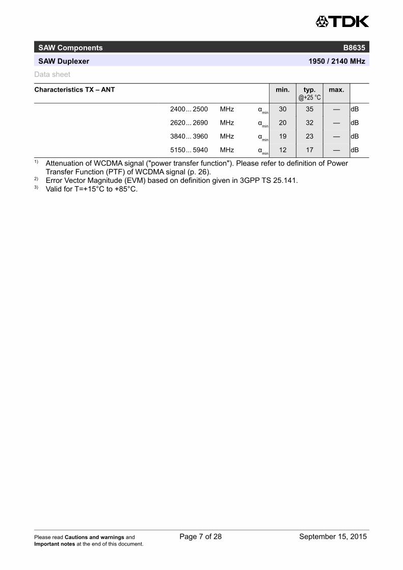
2400... 2500 MHz αmin
30 35 — dB
2620... 2690 MHz αmin
20 32 — dB
3840... 3960 MHz αmin
19 23 — dB
5150... 5940 MHz αmin
12 17 — dB
1) Attenuation of WCDMA signal ("power transfer function"). Please refer to definition of Power Transfer Function (PTF) of WCDMA signal (p. 26).
2) Error Vector Magnitude (EVM) based on definition given in 3GPP TS 25.141.3) Valid for T=+15°C to +85°C.
Please read Cautions and warnings and Page 7 of 28 September 15, 2015Important notes at the end of this document.

SAW Components B8635
SAW Duplexer 1950 / 2140 MHz
Data sheet
6.2 ANT – RX
Temperature range for specification T = −30 °C to +90 °CTX terminating impedance Z
TX= 50 Ω
ANT terminating impedance ZANT
= 50 Ω with par. 2.7 nH
RX terminating impedance ZRX
= 100 Ω with par. 10 nH
Characteristics ANT – RX min. typ.@+25 °C
max.
Center frequency fC
— 2140 — MHz
Maximum insertion attenuation
2110... 2170 MHz αmax
— 1.9 2.2 dB
@fcarrier
2112.4... 2167.6 MHz αWCDMA,max
1) — 1.9 2.1 dB
Amplitude ripple (p-p)
2110... 2170 MHz Δα — 0.3 0.7 dB
@fcarrier
2112.4... 2167.6 MHz ΔαWCDMA
1) — 0.3 0.7 dB
Maximum VSWR VSWRmax
@ ANT port 2110... 2170 MHz — 1.6 2.0
@ RX port 2110... 2170 MHz — 1.7 2.0
Maximum error vector magnitude EVMmax
2)
2112.4... 2167.6 MHz — 1.0 2.0 %
Minimum attenuation
10... 1920 MHz αmin
35 58 — dB
1920... 1980 MHz αmin
45 57 — dB
@fcarrier
1922.4... 1977.6 MHz αWCDMA,min
1) 45 57 — dB
1980... 2025 MHz αmin
15 37 — dB
2255... 2400 MHz αmin
15 44 — dB
2400... 2484 MHz αmin
30 44 — dB
2484... 6000 MHz αmin
35 45 — dB
IMD product levels3)
IMD2
Blocker 1 190 MHz — −130 −110 dBm
Blocker 3 4090 MHz — −117 −106 dBm
IMD3
Blocker 2 1760 MHz — −112 −104 dBm
Minimum common-mode rejection ratio CMRRmin
2110... 2170 MHz 194) 22 — dB
Please read Cautions and warnings and Page 8 of 28 September 15, 2015Important notes at the end of this document.
SAW Components B8635
SAW Duplexer 1950 / 2140 MHz
Data sheet
1) Attenuation of WCDMA signal ("power transfer function"). Please refer to definition of Power Transfer Function (PTF) of WCDMA signal (p. 26).
2) Error Vector Magnitude (EVM) based on definition given in 3GPP TS 25.141.3) @ f
TX = 1950.0 MHz, f
RX = 2140.0 MHz, f
RX - f
TX = 190 MHz, IMD product levels for power levels P
TX
= 21.5 dBm (ANT port output power) and Pblocker
= −15 dBm (ANT port input power).4) A combination of 10° phase balance and 1 dB amplitude balance corresponds to 19.6 dB CMRR.
Please read Cautions and warnings and Page 9 of 28 September 15, 2015Important notes at the end of this document.

SAW Components B8635
SAW Duplexer 1950 / 2140 MHz
Data sheet
6.3 TX – RX
Temperature range for specification T = −30 °C to +90 °CTX terminating impedance Z
TX= 50 Ω
ANT terminating impedance ZANT
= 50 Ω with par. 2.7 nH
RX terminating impedance ZRX
= 100 Ω with par. 10 nH
Characteristics TX – RX min. typ.@+25 °C
max.
Minimum differential-mode isolation
1920... 1975 MHz αmin
55 59 — dB
1920... 1980 MHz αmin
552) 59 — dB
@fcarrier
1922.4... 1977.6 MHz αWCDMA,min
1) 55 59 — dB
1975... 1980 MHz αmin
53 59 — dB
2110... 2170 MHz αmin
53 59 — dB
@fcarrier
2112.4... 2167.6 MHz αWCDMA,min
1) 53 59 — dB
3830... 3970 MHz αmin
20 54 — dB
5750... 5950 MHz αmin
20 49 — dB
Minimum common-mode isolation
1920... 1980 MHz αmin
47 50 — dB
@fcarrier
1922.4... 1977.6 MHz αWCDMA,min
1) 47 50 — dB
1) Attenuation of WCDMA signal ("power transfer function"). Please refer to definition of Power Transfer Function (PTF) of WCDMA signal (p. 26).
2) Valid for room temperature +25°C.
Please read Cautions and warnings and Page 10 of 28 September 15, 2015Important notes at the end of this document.

SAW Components B8635
SAW Duplexer 1950 / 2140 MHz
Data sheet
7 Maximum ratings
Storage temperature TSTG
= −40 °C to +85 °C
DC voltage VDC
= 5.0 V (max.)1)
ESD voltage
VESD
2) 50 V (max.) Machine model.
VESD
3) 250 V (max.) Human body model.
VESD
4) 600 V (max.) Charged device model.
Input power PIN
@ TX port: 1920 ... 1980 MHz 29 dBm Continuous wave for 5000 h @ 50 °C.
@ TX port: other frequency range(s) 10 dBm Continuous wave for 5000 h @ 50 °C.
1) 168h Damp Heat Steady State acc. IEC 60068-2-67 Cy.2) According to JESD22-A115B (MM – Machine Model), 10 negative & 10 positive pulses.3) According to JESD22-A114F (HBM – Human Body Model), 1 negative & 1 positive pulse.4) According to JESD22-C101C (CDM – Field Induced Charged Device Model), 3 negative & 3
positive pulses.
Please read Cautions and warnings and Page 11 of 28 September 15, 2015Important notes at the end of this document.

SAW Components B8635
SAW Duplexer 1950 / 2140 MHz
Data sheet
8 Transmission coefficients
8.1 TX – ANT
Please read Cautions and warnings and Page 12 of 28 September 15, 2015Important notes at the end of this document.
Figure 4: Attenuation TX – ANT.

SAW Components B8635
SAW Duplexer 1950 / 2140 MHz
Data sheet
8.2 ANT – RX
Please read Cautions and warnings and Page 13 of 28 September 15, 2015Important notes at the end of this document.
Figure 5: Attenuation ANT – RX.

SAW Components B8635
SAW Duplexer 1950 / 2140 MHz
Data sheet
8.3 TX – RX
Please read Cautions and warnings and Page 14 of 28 September 15, 2015Important notes at the end of this document.
Figure 6: Differential-mode isolation TX – RX.

SAW Components B8635
SAW Duplexer 1950 / 2140 MHz
Data sheet
Please read Cautions and warnings and Page 15 of 28 September 15, 2015Important notes at the end of this document.
Figure 7: Common-mode isolation TX – RX.

SAW Components B8635
SAW Duplexer 1950 / 2140 MHz
Data sheet
9 Reflection coefficients
Figure 8: Reflection coefficient at TX port.
Figure 9: Reflection coefficient at ANT port (TX and RX frequencies).
Figure 10: Reflection coefficient at RX port.
Please read Cautions and warnings and Page 16 of 28 September 15, 2015Important notes at the end of this document.

SAW Components B8635
SAW Duplexer 1950 / 2140 MHz
Data sheet
10 EVMs
10.1 TX – ANT
Please read Cautions and warnings and Page 17 of 28 September 15, 2015Important notes at the end of this document.
Figure 11: Error vector magnitude TX – ANT.
SAW Components B8635
SAW Duplexer 1950 / 2140 MHz
Data sheet
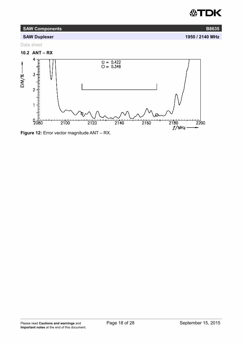
10.2 ANT – RX
Please read Cautions and warnings and Page 18 of 28 September 15, 2015Important notes at the end of this document.
Figure 12: Error vector magnitude ANT – RX.
SAW Components B8635
SAW Duplexer 1950 / 2140 MHz
Data sheet
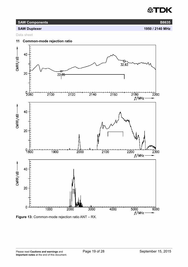
11 Common-mode rejection ratio
Please read Cautions and warnings and Page 19 of 28 September 15, 2015Important notes at the end of this document.
Figure 13: Common-mode rejection ratio ANT – RX.

SAW Components B8635
SAW Duplexer 1950 / 2140 MHz
Data sheet
12 Packing material
12.1 Tape
A0 1.62±0.05 mm E2 6.25 mm (min.) P1 4.0±0.1 mm
B0 2.04±0.05 mm F 3.5±0.05 mm P2 2.0±0.05 mm
D0 1.5±0.05 mm G 0.75 mm (min.) T 0.25±0.02 mm
D1 0.8±0.05 mm K0 0.62±0.05 mm W 8.0±0.1 mm
E1 1.75±0.1 mm P0 4.0±0.1 mm
Table 1: Tape dimensions.
12.2 Reel with diameter of 180 mm
Figure 15: Drawing of reel (first-angle projection) with diameter of 180 mm.
Please read Cautions and warnings and Page 20 of 28 September 15, 2015Important notes at the end of this document.
Figure 14: Drawing of tape (first-angle projection) with tape dimensions according to Table 1.

SAW Components B8635
SAW Duplexer 1950 / 2140 MHz
Data sheet
Figure 16: Drawing of moisture barrier bag (MBB) for reel withdiameter of 180 mm.
Figure 17: Drawing of folding box for reel with diameter of 180 mm.
Please read Cautions and warnings and Page 21 of 28 September 15, 2015Important notes at the end of this document.

SAW Components B8635
SAW Duplexer 1950 / 2140 MHz
Data sheet
12.3 Reel with diameter of 330 mm
Figure 18: Drawing of reel (first-angle projection) with diameter of 330 mm.
Figure 19: Drawing of moisture barrier bag (MBB) for reel withdiameter of 330 mm.
Please read Cautions and warnings and Page 22 of 28 September 15, 2015Important notes at the end of this document.

SAW Components B8635
SAW Duplexer 1950 / 2140 MHz
Data sheet
Figure 20: Drawing of folding box for reel with diameter of 330 mm.
13 Marking
Products are marked with product type number and lot number encoded according to Table 2:
Type number:
The 4 digit type number of the ordering code, e.g., B3xxxxB1234xxxx,is encoded by a special BASE32 code into a 3 digit marking.
Example of decoding type number marking on device in decimal code.16J => 1234 1 x 322 + 6 x 321 + 18 (=J) x 320 = 1234
The BASE32 code for product type B8635 is 8DV.
Lot number:
The last 5 digits of the lot number, e.g., 12345,are encoded based on a special BASE47 code into a 3 digit marking.
Example of decoding lot number marking on device in decimal code.5UY => 123455 x 472 + 27 (=U) x 471 + 31 (=Y) x 470 = 12345
Please read Cautions and warnings and Page 23 of 28 September 15, 2015Important notes at the end of this document.

SAW Components B8635
SAW Duplexer 1950 / 2140 MHz
Data sheet
Please read Cautions and warnings and Page 24 of 28 September 15, 2015Important notes at the end of this document.
Adopted BASE32 code for type number Adopted BASE47 code for lot numberDecimal
valueBase32
codeDecimal
valueBase32
codeDecimal
valueBase47
codeDecimal
valueBase47
code0 0 16 G 0 0 24 R1 1 17 H 1 1 25 S2 2 18 J 2 2 26 T3 3 19 K 3 3 27 U4 4 20 M 4 4 28 V5 5 21 N 5 5 29 W6 6 22 P 6 6 30 X7 7 23 Q 7 7 31 Y8 8 24 R 8 8 32 Z9 9 25 S 9 9 33 b
10 A 26 T 10 A 34 d11 B 27 V 11 B 35 f12 C 28 W 12 C 36 h13 D 29 X 13 D 37 n14 E 30 Y 14 E 38 r15 F 31 Z 15 F 39 t
16 G 40 v17 H 41 \18 J 42 ?19 K 43 20 L 44 21 M 45 <22 N 46 >23 P
Table 2: Lists for encoding and decoding of marking.
SAW Components B8635
SAW Duplexer 1950 / 2140 MHz
Data sheet
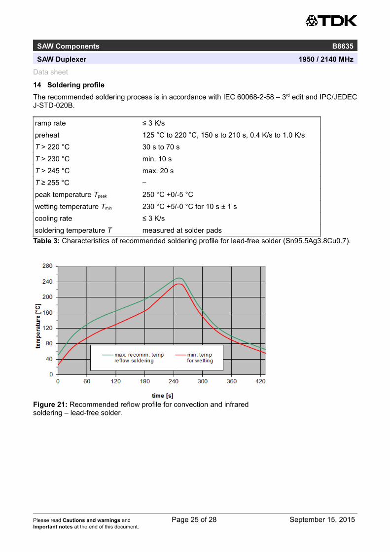
14 Soldering profile
The recommended soldering process is in accordance with IEC 60068-2-58 – 3rd edit and IPC/JEDECJ-STD-020B.
Please read Cautions and warnings and Page 25 of 28 September 15, 2015Important notes at the end of this document.
Figure 21: Recommended reflow profile for convection and infrared soldering – lead-free solder.
ramp rate ≤ 3 K/s
preheat 125 °C to 220 °C, 150 s to 210 s, 0.4 K/s to 1.0 K/s
T > 220 °C 30 s to 70 s
T > 230 °C min. 10 s
T > 245 °C max. 20 s
T ≥ 255 °C –
peak temperature Tpeak 250 °C +0/-5 °C
wetting temperature Tmin 230 °C +5/-0 °C for 10 s ± 1 s
cooling rate ≤ 3 K/s
soldering temperature T measured at solder pads
Table 3: Characteristics of recommended soldering profile for lead-free solder (Sn95.5Ag3.8Cu0.7).

SAW Components B8635
SAW Duplexer 1950 / 2140 MHz
Data sheet
15 Annotations
15.1 Matching coils
See TDK inductor pdf-catalog http://www.tdk.co.jp/tefe02/coil.htm#aname1 and Data Library for circuitsimulation http://www.tdk.co.jp/etvcl/index.htm.
15.2 Power Transfer Function (PTF) of WCDMA signal
Attenuation of WCDMA signal, αWCDMA
, is defined by
αWCDMA( f carrier)=10 log10∣ 1PTF ( f carrier)∣dB
and
PTF( f carrier)=∫−∞
+∞
∣S 21( f )H RRC( f − f carrier)∣2d f
with fcarrier according to 3GPP TS 25.101 (e.g., for the WCDMA B8 pass band, fcarrier ranges from 882.4 MHz to 912.6 MHz which correspond to the lowest and highest TX channels, respectively). HRRC(f) is the transfer function of the root-raised cosine transmit pulse shaping filter according to 3GPP TS 25.101 using the normalization
∫−∞
+∞
∣H RRC( f )∣2d f =1 .
15.3 RoHS compatibility
ROHS-compatible means that products are compatible with the requirements according to Art. 4 (substance restrictions) of Directive 2011/65/EU of the European Parliament and of the Council of June 8th, 2011, on the restriction of the use of certain hazardous substances in electrical and electronic equipment ("Directive") with due regard to the application of exemptions as per Annex III of the Directive in certain cases.
15.4 Scattering parameters (S-parameters)
The pin/port assignment is available in the headers of the S-parameter files. Please contact your localEPCOS sales office.
15.5 Ordering code and packing units
16 Cautions and warnings
16.1 Moldability
Before using in overmolding environment, please contact your local EPCOS sales office.
16.2 Simplified drawings
Landing area
The printed circuit board (PCB) land pattern (landing area) shown is based on EPCOS internal
Please read Cautions and warnings and Page 26 of 28 September 15, 2015Important notes at the end of this document.
Ordering code Packing units
B39212B8635P810 15000 pcs
B39212B8635P810S 5 5000 pcs
Table 4: Ordering codes and packing units.

SAW Components B8635
SAW Duplexer 1950 / 2140 MHz
Data sheet
development and empirical data and illustrated for example purposes, only. As customers' SMD assembly processes may have a plenty of variants and influence factors which are not under control or knowledge of EPCOS, additional careful process development on customer side is necessary and strongly recommended in order to achieve best soldering results tailored to the particular customer needs.
Dimensions
Unless otherwise specified all dimensions are understood using unit millimeter (mm).
Projection method
Unless otherwise specified first-angle projection is applied.
Please read Cautions and warnings and Page 27 of 28 September 15, 2015Important notes at the end of this document.
Contact and Important notes
For further information please contact your local EPCOS sales office or visit our web page atwww.epcos.com.
Published by EPCOS AGSystems, Acoustics, Waves Business GroupP.O. Box 80 17 09, 81617 Munich, GERMANY
© EPCOS AG 2015. This brochure replaces the previous edition.
For questions on technology, prices and delivery please contact the sales offices of EPCOS AG or theinternational representatives.
Due to technical requirements components may contain dangerous substances. For information on the type in question please also contact one of our sales offices.

Important notes
The following applies to all products named in this publication:
1. Some parts of this publication contain statements about the suitability of our products forcertain areas of application. These statements are based on our knowledge of typicalrequirements that are often placed on our products in the areas of application concerned. Wenevertheless expressly point out that such statements cannot be regarded as bindingstatements about the suitability of our products for a particular customer application.As a rule, EPCOS is either unfamiliar with individual customer applications or less familiar withthem than the customers themselves. For these reasons, it is always ultimately incumbent onthe customer to check and decide whether an EPCOS product with the properties described inthe product specification is suitable for use in a particular customer application.
2. We also point out that in individual cases, a malfunction of electronic components orfailure before the end of their usual service life cannot be completely ruled out in thecurrent state of the art, even if they are operated as specified. In customer applicationsrequiring a very high level of operational safety and especially in customer applications inwhich the malfunction or failure of an electronic component could endanger human life orhealth (e.g. in accident prevention or life-saving systems), it must therefore be ensured bymeans of suitable design of the customer application or other action taken by the customer(e.g. installation of protective circuitry or redundancy) that no injury or damage is sustained bythird parties in the event of malfunction or failure of an electronic component.
3. The warnings, cautions and product-specific notes must be observed.
4. In order to satisfy certain technical requirements, some of the products described in thispublication may contain substances subject to restrictions in certain jurisdictions (e.g.because they are classed as hazardous). Useful information on this will be found in ourMaterial Data Sheets on the Internet (www.epcos.com/material). Should you have any moredetailed questions, please contact our sales offices.
5. We constantly strive to improve our products. Consequently, the products described in thispublication may change from time to time. The same is true of the corresponding productspecifications. Please check therefore to what extent product descriptions and specificationscontained in this publication are still applicable before or when you place an order.We also reserve the right to discontinue production and delivery of products.Consequently, we cannot guarantee that all products named in this publication will always beavailable. The aforementioned does not apply in the case of individual agreements deviating from theforegoing for customer-specific products.
6. Unless otherwise agreed in individual contracts, all orders are subject to the currentversion of the “General Terms of Delivery for Products and Services in the ElectricalIndustry” published by the German Electrical and Electronics Industry Association(ZVEI).
7. The trade names EPCOS, Alu-X, CeraDiode, CeraLink, CeraPad, CeraPlas, CSMP, CSSP,CTVS, DeltaCap, DigiSiMic, DSSP, ExoCore, FilterCap, FormFit, LeaXield, MiniBlue, MiniCell,MKD, MKK, MotorCap, PCC, PhaseCap, PhaseCube, PhaseMod, PhiCap, PQSine,SIFERRIT, SIFI, SIKOREL, SilverCap, SIMDAD, SiMic, SIMID, SineFormer, SIOV, SIP5D,SIP5K, TFAP, ThermoFuse, WindCap are trademarks registered or pending in Europe andin other countries. Further information will be found on the Internet atwww.epcos.com/trademarks.
Page 28 of 28